EP3309155B1 - Host-materialien für pholeds - Google Patents
Host-materialien für pholeds Download PDFInfo
- Publication number
- EP3309155B1 EP3309155B1 EP17198124.4A EP17198124A EP3309155B1 EP 3309155 B1 EP3309155 B1 EP 3309155B1 EP 17198124 A EP17198124 A EP 17198124A EP 3309155 B1 EP3309155 B1 EP 3309155B1
- Authority
- EP
- European Patent Office
- Prior art keywords
- bond
- compound
- group
- layer
- organic
- Prior art date
- Legal status (The legal status is an assumption and is not a legal conclusion. Google has not performed a legal analysis and makes no representation as to the accuracy of the status listed.)
- Active
Links
- 0 CC(*(c1c2cccc1)C1=C(C)C=C*(*)C=C1)*2(*)O Chemical compound CC(*(c1c2cccc1)C1=C(C)C=C*(*)C=C1)*2(*)O 0.000 description 13
- DKHNGUNXLDCATP-UHFFFAOYSA-N N#Cc(nc1c(nc2C#N)c3nc2C#N)c(C#N)nc1c(nc1C#N)c3nc1C#N Chemical compound N#Cc(nc1c(nc2C#N)c3nc2C#N)c(C#N)nc1c(nc1C#N)c3nc1C#N DKHNGUNXLDCATP-UHFFFAOYSA-N 0.000 description 2
- OEOUOPOZQPGRLR-UHFFFAOYSA-N Brc(cccc1c2c3cccc2)c1[n]3-c1nc(-c2ccccc2)nc(-c2ccccc2)n1 Chemical compound Brc(cccc1c2c3cccc2)c1[n]3-c1nc(-c2ccccc2)nc(-c2ccccc2)n1 OEOUOPOZQPGRLR-UHFFFAOYSA-N 0.000 description 1
- VCDOOGZTWDOHEB-UHFFFAOYSA-N Brc1cccc2c1[nH]c1ccccc21 Chemical compound Brc1cccc2c1[nH]c1ccccc21 VCDOOGZTWDOHEB-UHFFFAOYSA-N 0.000 description 1
- ACWBJEDBTSYZMJ-UHFFFAOYSA-N CC(Nc1c2nccc1)N2c1c(C)cccc1 Chemical compound CC(Nc1c2nccc1)N2c1c(C)cccc1 ACWBJEDBTSYZMJ-UHFFFAOYSA-N 0.000 description 1
- DDGPPAMADXTGTN-UHFFFAOYSA-N Clc1nc(-c2ccccc2)nc(-c2ccccc2)n1 Chemical compound Clc1nc(-c2ccccc2)nc(-c2ccccc2)n1 DDGPPAMADXTGTN-UHFFFAOYSA-N 0.000 description 1
- JNNZFNFSIJORDK-UHFFFAOYSA-N Fc(c(-c(c(F)c(c(F)c1F)F)c1F)c(c(F)c1-c2nc(-c(c(F)c(c(F)c3F)F)c3F)nc(-c(c(F)c(c(F)c3F)F)c3F)n2)F)c1F Chemical compound Fc(c(-c(c(F)c(c(F)c1F)F)c1F)c(c(F)c1-c2nc(-c(c(F)c(c(F)c3F)F)c3F)nc(-c(c(F)c(c(F)c3F)F)c3F)n2)F)c1F JNNZFNFSIJORDK-UHFFFAOYSA-N 0.000 description 1
- SDHNJSIZTIODFW-UHFFFAOYSA-N c(cc1)cc(c2c3cccc2)c1[n]3-c(cc1c2c3)ccc1[s]c2ccc3-[n]1c2ccccc2c2c1cccc2 Chemical compound c(cc1)cc(c2c3cccc2)c1[n]3-c(cc1c2c3)ccc1[s]c2ccc3-[n]1c2ccccc2c2c1cccc2 SDHNJSIZTIODFW-UHFFFAOYSA-N 0.000 description 1
- NSXJEEMTGWMJPY-UHFFFAOYSA-N c(cc1)cc(c2ccccc22)c1[n]2-c1cccc(-c2cc(-[n]3c(cccc4)c4c4c3cccc4)ccc2)c1 Chemical compound c(cc1)cc(c2ccccc22)c1[n]2-c1cccc(-c2cc(-[n]3c(cccc4)c4c4c3cccc4)ccc2)c1 NSXJEEMTGWMJPY-UHFFFAOYSA-N 0.000 description 1
- ICVRMAPETUQKIA-UHFFFAOYSA-N c(cc1)ccc1-c1nnc(-c(cc2)ccc2-c2nnc(-c3ccccc3)[o]2)[n]1-c1ccccc1 Chemical compound c(cc1)ccc1-c1nnc(-c(cc2)ccc2-c2nnc(-c3ccccc3)[o]2)[n]1-c1ccccc1 ICVRMAPETUQKIA-UHFFFAOYSA-N 0.000 description 1
- AOQKGYRILLEVJV-UHFFFAOYSA-N c(cc1)ccc1-c1nnc(-c2ccccc2)[n]1-c1cccc2ccccc12 Chemical compound c(cc1)ccc1-c1nnc(-c2ccccc2)[n]1-c1cccc2ccccc12 AOQKGYRILLEVJV-UHFFFAOYSA-N 0.000 description 1
- LYXTZYYMWXCIFZ-UHFFFAOYSA-N c(cc1C2(c(cc3)ccc3Oc(cc3)ccc3-[n]3c(cccc4)c4c4c3cccc4)c(cc3)ccc3Oc(cc3)ccc3-[n]3c4ccccc4c4ccccc34)ccc1-c1c2cccc1 Chemical compound c(cc1C2(c(cc3)ccc3Oc(cc3)ccc3-[n]3c(cccc4)c4c4c3cccc4)c(cc3)ccc3Oc(cc3)ccc3-[n]3c4ccccc4c4ccccc34)ccc1-c1c2cccc1 LYXTZYYMWXCIFZ-UHFFFAOYSA-N 0.000 description 1
Images


Classifications
-
- C—CHEMISTRY; METALLURGY
- C07—ORGANIC CHEMISTRY
- C07D—HETEROCYCLIC COMPOUNDS
- C07D403/00—Heterocyclic compounds containing two or more hetero rings, having nitrogen atoms as the only ring hetero atoms, not provided for by group C07D401/00
- C07D403/02—Heterocyclic compounds containing two or more hetero rings, having nitrogen atoms as the only ring hetero atoms, not provided for by group C07D401/00 containing two hetero rings
- C07D403/04—Heterocyclic compounds containing two or more hetero rings, having nitrogen atoms as the only ring hetero atoms, not provided for by group C07D401/00 containing two hetero rings directly linked by a ring-member-to-ring-member bond
-
- C—CHEMISTRY; METALLURGY
- C07—ORGANIC CHEMISTRY
- C07D—HETEROCYCLIC COMPOUNDS
- C07D403/00—Heterocyclic compounds containing two or more hetero rings, having nitrogen atoms as the only ring hetero atoms, not provided for by group C07D401/00
- C07D403/02—Heterocyclic compounds containing two or more hetero rings, having nitrogen atoms as the only ring hetero atoms, not provided for by group C07D401/00 containing two hetero rings
- C07D403/10—Heterocyclic compounds containing two or more hetero rings, having nitrogen atoms as the only ring hetero atoms, not provided for by group C07D401/00 containing two hetero rings linked by a carbon chain containing aromatic rings
-
- C—CHEMISTRY; METALLURGY
- C07—ORGANIC CHEMISTRY
- C07D—HETEROCYCLIC COMPOUNDS
- C07D471/00—Heterocyclic compounds containing nitrogen atoms as the only ring hetero atoms in the condensed system, at least one ring being a six-membered ring with one nitrogen atom, not provided for by groups C07D451/00 - C07D463/00
- C07D471/02—Heterocyclic compounds containing nitrogen atoms as the only ring hetero atoms in the condensed system, at least one ring being a six-membered ring with one nitrogen atom, not provided for by groups C07D451/00 - C07D463/00 in which the condensed system contains two hetero rings
- C07D471/04—Ortho-condensed systems
-
- C—CHEMISTRY; METALLURGY
- C09—DYES; PAINTS; POLISHES; NATURAL RESINS; ADHESIVES; COMPOSITIONS NOT OTHERWISE PROVIDED FOR; APPLICATIONS OF MATERIALS NOT OTHERWISE PROVIDED FOR
- C09K—MATERIALS FOR MISCELLANEOUS APPLICATIONS, NOT PROVIDED FOR ELSEWHERE
- C09K11/00—Luminescent materials, e.g. electroluminescent or chemiluminescent
- C09K11/06—Luminescent materials, e.g. electroluminescent or chemiluminescent containing organic luminescent materials
-
- H—ELECTRICITY
- H10—SEMICONDUCTOR DEVICES; ELECTRIC SOLID-STATE DEVICES NOT OTHERWISE PROVIDED FOR
- H10K—ORGANIC ELECTRIC SOLID-STATE DEVICES
- H10K50/00—Organic light-emitting devices
- H10K50/10—OLEDs or polymer light-emitting diodes [PLED]
- H10K50/11—OLEDs or polymer light-emitting diodes [PLED] characterised by the electroluminescent [EL] layers
-
- H—ELECTRICITY
- H10—SEMICONDUCTOR DEVICES; ELECTRIC SOLID-STATE DEVICES NOT OTHERWISE PROVIDED FOR
- H10K—ORGANIC ELECTRIC SOLID-STATE DEVICES
- H10K50/00—Organic light-emitting devices
- H10K50/10—OLEDs or polymer light-emitting diodes [PLED]
- H10K50/18—Carrier blocking layers
- H10K50/181—Electron blocking layers
-
- H—ELECTRICITY
- H10—SEMICONDUCTOR DEVICES; ELECTRIC SOLID-STATE DEVICES NOT OTHERWISE PROVIDED FOR
- H10K—ORGANIC ELECTRIC SOLID-STATE DEVICES
- H10K85/00—Organic materials used in the body or electrodes of devices covered by this subclass
- H10K85/60—Organic compounds having low molecular weight
- H10K85/649—Aromatic compounds comprising a hetero atom
- H10K85/654—Aromatic compounds comprising a hetero atom comprising only nitrogen as heteroatom
-
- H—ELECTRICITY
- H10—SEMICONDUCTOR DEVICES; ELECTRIC SOLID-STATE DEVICES NOT OTHERWISE PROVIDED FOR
- H10K—ORGANIC ELECTRIC SOLID-STATE DEVICES
- H10K85/00—Organic materials used in the body or electrodes of devices covered by this subclass
- H10K85/60—Organic compounds having low molecular weight
- H10K85/649—Aromatic compounds comprising a hetero atom
- H10K85/657—Polycyclic condensed heteroaromatic hydrocarbons
- H10K85/6572—Polycyclic condensed heteroaromatic hydrocarbons comprising only nitrogen in the heteroaromatic polycondensed ring system, e.g. phenanthroline or carbazole
-
- H—ELECTRICITY
- H10—SEMICONDUCTOR DEVICES; ELECTRIC SOLID-STATE DEVICES NOT OTHERWISE PROVIDED FOR
- H10K—ORGANIC ELECTRIC SOLID-STATE DEVICES
- H10K2101/00—Properties of the organic materials covered by group H10K85/00
- H10K2101/10—Triplet emission
Definitions
- the present disclosure generally relates to novel compounds containing carbazole and triazine with different number of phenyl units attached to their core.
- the disclosure relates to compositions and/or devices comprising these compounds as hosts for PHOLEDs.
- Opto-electronic devices that make use of organic materials are becoming increasingly desirable for a number of reasons. Many of the materials used to make such devices are relatively inexpensive, so organic opto-electronic devices have the potential for cost advantages over inorganic devices. In addition, the inherent properties of organic materials, such as their flexibility, may make them well suited for particular applications such as fabrication on a flexible substrate. Examples of organic opto-electronic devices include organic light emitting devices (OLEDs), organic phototransistors, organic photovoltaic cells, and organic photodetectors. For OLEDs, the organic materials may have performance advantages over conventional materials. For example, the wavelength at which an organic emissive layer emits light may generally be readily tuned with appropriate dopants.
- OLEDs organic light emitting devices
- the wavelength at which an organic emissive layer emits light may generally be readily tuned with appropriate dopants.
- OLEDs make use of thin organic films that emit light when voltage is applied across the device. OLEDs are becoming an increasingly interesting technology for use in applications such as flat panel displays, illumination, and backlighting. Several OLED materials and configurations are described in U.S. Pat. Nos. 5,844,363 , 6,303,238 , and 5,707,745 .
- phosphorescent emissive molecules is a full color display.
- Industry standards for such a display call for pixels adapted to emit particular colors, referred to as "saturated" colors.
- these standards call for saturated red, green, and blue pixels. Color may be measured using CIE coordinates, which are well known to the art.
- a green emissive molecule is tris(2-phenylpyridine) iridium, denoted Ir(ppy) 3 , which has the following structure:
- organic includes polymeric materials as well as small molecule organic materials that may be used to fabricate organic opto-electronic devices.
- Small molecule refers to any organic material that is not a polymer, and "small molecules” may actually be quite large. Small molecules may include repeat units in some circumstances. For example, using a long chain alkyl group as a substituent does not remove a molecule from the "small molecule” class. Small molecules may also be incorporated into polymers, for example as a pendent group on a polymer backbone or as a part of the backbone. Small molecules may also serve as the core moiety of a dendrimer, which consists of a series of chemical shells built on the core moiety.
- the core moiety of a dendrimer may be a fluorescent or phosphorescent small molecule emitter.
- a dendrimer may be a "small molecule,” and it is believed that all dendrimers currently used in the field of OLEDs are small molecules.
- top means furthest away from the substrate, while “bottom” means closest to the substrate.
- first layer is described as “disposed over” a second layer, the first layer is disposed further away from substrate. There may be other layers between the first and second layer, unless it is specified that the first layer is "in contact with” the second layer.
- a cathode may be described as “disposed over” an anode, even though there are various organic layers in between.
- solution processible means capable of being dissolved, dispersed, or transported in and/or deposited from a liquid medium, either in solution or suspension form.
- a ligand may be referred to as "photoactive” when it is believed that the ligand directly contributes to the photoactive properties of an emissive material.
- a ligand may be referred to as "ancillary” when it is believed that the ligand does not contribute to the photoactive properties of an emissive material, although an ancillary ligand may alter the properties of a photoactive ligand.
- a first "Highest Occupied Molecular Orbital” (HOMO) or “Lowest Unoccupied Molecular Orbital” (LUMO) energy level is “greater than” or "higher than” a second HOMO or LUMO energy level if the first energy level is closer to the vacuum energy level.
- IP ionization potentials
- a higher HOMO energy level corresponds to an IP having a smaller absolute value (an IP that is less negative).
- a higher LUMO energy level corresponds to an electron affinity (EA) having a smaller absolute value (an EA that is less negative).
- the LUMO energy level of a material is higher than the HOMO energy level of the same material.
- a "higher” HOMO or LUMO energy level appears closer to the top of such a diagram than a "lower” HOMO or LUMO energy level.
- a first work function is "greater than” or “higher than” a second work function if the first work function has a higher absolute value. Because work functions are generally measured as negative numbers relative to vacuum level, this means that a "higher” work function is more negative. On a conventional energy level diagram, with the vacuum level at the top, a “higher” work function is illustrated as further away from the vacuum level in the downward direction. Thus, the definitions of HOMO and LUMO energy levels follow a different convention than work functions.
- the present invention is directed to a compound having a structure according to Formula II:
- the compound having a structure according to Formula II is selected from the group consisting of Compound 1 through Compound 161 and Compound 302 through 462, listed in the table below, wherein Y 1 , R 1 , R 2 , R 3 , R 4 , R 5 and L are as defined and wherein C is Carbon, N is nitrogen, H is hydrogen, A 1 is A 2 is A 6 is
- the compound is selected from the group consisting of:
- a formulation comprising a compound of Formula II is provided.
- a device comprising a organic light emitting device, the organic light emitting device comprising: an anode; a cathode; an organic layer, disposed between the anode and the cathode, wherein the organic layer further comprising a compound having a structure according to Formula II as defined herein.
- the device is an organic light-emitting device. In one embodiment, the device comprises a lighting panel. In one embodiment, the compound is selected from the group consisting of:
- the compound is selected from Compounds 1 through 161. In one embodiment, the compound is selected from Compounds 302 to 462.
- the device is a consumer product.
- the organic layer is an emissive layer and the compound of Formula II is a host.
- the organic layer is a blocking layer and the compound having Formula II is a blocking material in the organic layer.
- the organic layer is an electron transporting layer and the compound having Formula II is an electron transporting material in the organic layer.
- an OLED comprises at least one organic layer disposed between and electrically connected to an anode and a cathode.
- the anode injects holes and the cathode injects electrons into the organic layer(s).
- the injected holes and electrons each migrate toward the oppositely charged electrode.
- an "exciton" which is a localized electron-hole pair having an excited energy state, is formed.
- Light is emitted when the exciton relaxes via a photoemissive mechanism.
- the exciton may be localized on an excimer or an exciplex. Non-radiative mechanisms, such as thermal relaxation, may also occur, but are generally considered undesirable.
- the initial OLEDs used emissive molecules that emitted light from their singlet states ("fluorescence") as disclosed, for example, in U.S. Pat. No. 4,769,292 . Fluorescent emission generally occurs in a time frame of less than 10 nanoseconds.
- FIG. 1 shows an organic light emitting device 100.
- Device 100 may include a substrate 110, an anode 115, a hole injection layer 120, a hole transport layer 125, an electron blocking layer 130, an emissive layer 135, a hole blocking layer 140, an electron transport layer 145, an electron injection layer 150, a protective layer 155, a cathode 160, and a barrier layer 170.
- Cathode 160 is a compound cathode having a first conductive layer 162 and a second conductive layer 164.
- Device 100 may be fabricated by depositing the layers described, in order. The properties and functions of these various layers, as well as example materials, are described in more detail in US 7,279,704 at cols. 6-10.
- a flexible and transparent substrate-anode combination is disclosed in U.S. Pat. No. 5,844,363 .
- An example of a p-doped hole transport layer is m-MTDATA doped with F 4 -TCNQ at a molar ratio of 50:1, as disclosed in U.S. Patent Application Publication No. 2003/0230980 .
- Examples of emissive and host materials are disclosed in U.S. Pat. No. 6,303,238 to Thompson et al.
- An example of an n-doped electron transport layer is BPhen doped with Li at a molar ratio of 1:1, as disclosed in U.S. Patent Application Publication No. 2003/0230980 .
- Pat. Nos. 5,703,436 and 5,707,745 disclose examples of cathodes including compound cathodes having a thin layer of metal such as Mg:Ag with an overlying transparent, electrically-conductive, sputter-deposited ITO layer.
- the theory and use of blocking layers is described in more detail in U.S. Pat. No. 6,097,147 and U.S. Patent Application Publication No. 2003/0230980 .
- Examples of injection layers are provided in U.S. Patent Application Publication No. 2004/0174116 .
- a description of protective layers may be found in U.S. Patent Application Publication No. 2004/0174116 .
- FIG. 2 shows an inverted OLED 200.
- the device includes a substrate 210, a cathode 215, an emissive layer 220, a hole transport layer 225, and an anode 230.
- Device 200 may be fabricated by depositing the layers described, in order. Because the most common OLED configuration has a cathode disposed over the anode, and device 200 has cathode 215 disposed under anode 230, device 200 may be referred to as an "inverted" OLED. Materials similar to those described with respect to device 100 may be used in the corresponding layers of device 200.
- FIG. 2 provides one example of how some layers may be omitted from the structure of device 100.
- FIGS. 1 and 2 The simple layered structure illustrated in FIGS. 1 and 2 is provided by way of non-limiting example, and it is understood that embodiments of the invention may be used in connection with a wide variety of other structures.
- the specific materials and structures described are exemplary in nature, and other materials and structures may be used.
- Functional OLEDs may be achieved by combining the various layers described in different ways, or layers may be omitted entirely, based on design, performance, and cost factors. Other layers not specifically described may also be included. Materials other than those specifically described may be used. Although many of the examples provided herein describe various layers as comprising a single material, it is understood that combinations of materials, such as a mixture of host and dopant, or more generally a mixture, may be used. Also, the layers may have various sublayers.
- hole transport layer 225 transports holes and injects holes into emissive layer 220, and may be described as a hole transport layer or a hole injection layer.
- an OLED may be described as having an "organic layer" disposed between a cathode and an anode. This organic layer may comprise a single layer, or may further comprise multiple layers of different organic materials as described, for example, with respect to FIGS. 1 and 2 .
- OLEDs comprised of polymeric materials (PLEDs) such as disclosed in U.S. Pat. No. 5,247,190 to Friend et al.
- PLEDs polymeric materials
- OLEDs having a single organic layer may be used.
- OLEDs may be stacked, for example as described in U.S. Pat. No. 5,707,745 to Forrest et al.
- the OLED structure may deviate from the simple layered structure illustrated in FIGS. 1 and 2 .
- the substrate may include an angled reflective surface to improve out-coupling, such as a mesa structure as described in U.S. Pat. No. 6,091,195 to Forrest et al. , and/or a pit structure as described in U.S. Pat. No. 5,834,893 to Bulovic et al.
- any of the layers of the various embodiments may be deposited by any suitable method.
- preferred methods include thermal evaporation, ink-jet, such as described in U.S. Pat. Nos. 6,013,982 and 6,087,196 , organic vapor phase deposition (OVPD), such as described in U.S. Pat. No. 6,337,102 to Forrest et al. , and deposition by organic vapor jet printing (OVJP), such as described in U.S. Pat. No. 7,431,968 .
- OVPD organic vapor phase deposition
- OJP organic vapor jet printing
- Other suitable deposition methods include spin coating and other solution based processes. Solution based processes are preferably carried out in nitrogen or an inert atmosphere.
- preferred methods include thermal evaporation.
- Preferred patterning methods include deposition through a mask, cold welding such as described in U.S. Pat. Nos. 6,294,398 and 6,468,819 , and patterning associated with some of the deposition methods such as ink-jet and OVJD. Other methods may also be used.
- the materials to be deposited may be modified to make them compatible with a particular deposition method.
- substituents such as alkyl and aryl groups, branched or unbranched, and preferably containing at least 3 carbons, may be used in small molecules to enhance their ability to undergo solution processing. Substituents having 20 carbons or more may be used, and 3-20 carbons is a preferred range. Materials with asymmetric structures may have better solution processibility than those having symmetric structures, because asymmetric materials may have a lower tendency to recrystallize. Dendrimer substituents may be used to enhance the ability of small molecules to undergo solution processing.
- Devices fabricated in accordance with embodiments of the present invention may further optionally comprise a barrier layer.
- a barrier layer One purpose of the barrier layer is to protect the electrodes and organic layers from damaging exposure to harmful species in the environment including moisture, vapor and/or gases, etc.
- the barrier layer may be deposited over, under or next to a substrate, an electrode, or over any other parts of a device including an edge.
- the barrier layer may comprise a single layer, or multiple layers.
- the barrier layer may be formed by various known chemical vapor deposition techniques and may include compositions having a single phase as well as compositions having multiple phases. Any suitable material or combination of materials may be used for the barrier layer.
- the barrier layer may incorporate an inorganic or an organic compound or both.
- the preferred barrier layer comprises a mixture of a polymeric material and a non-polymeric material as described in U.S. Pat. No. 7,968,146 , PCT Pat. Application Nos. PCT/US2007/023098 and PCT/US2009/042829 .
- the aforesaid polymeric and non-polymeric materials comprising the barrier layer should be deposited under the same reaction conditions and/or at the same time.
- the weight ratio of polymeric to non-polymeric material may be in the range of 95:5 to 5:95.
- the polymeric material and the non-polymeric material may be created from the same precursor material.
- the mixture of a polymeric material and a non-polymeric material consists essentially of polymeric silicon and inorganic silicon.
- Devices fabricated in accordance with embodiments of the invention may be incorporated into a wide variety of consumer products, including flat panel displays, computer monitors, medical monitors, televisions, billboards, lights for interior or exterior illumination and/or signaling, heads up displays, fully transparent displays, flexible displays, laser printers, telephones, cell phones, personal digital assistants (PDAs), laptop computers, digital cameras, camcorders, viewfinders, micro-displays, vehicles, a large area wall, theater or stadium screen, or a sign.
- PDAs personal digital assistants
- Various control mechanisms may be used to control devices fabricated in accordance with the present invention, including passive matrix and active matrix. Many of the devices are intended for use in a temperature range comfortable to humans, such as 18 degrees C. to 30 degrees C., and more preferably at room temperature (20-25 degrees C.).
- the materials and structures described herein may have applications in devices other than OLEDs.
- other optoelectronic devices such as organic solar cells and organic photodetectors may employ the materials and structures.
- organic devices such as organic transistors, may employ the materials and structures.
- halo, halogen, alkyl, cycloalkyl, alkenyl, alkynyl, arylkyl, heterocyclic group, aryl, aromatic group, and heteroaryl are known to the art, and are defined in US 7,279,704 at cols. 31-32.
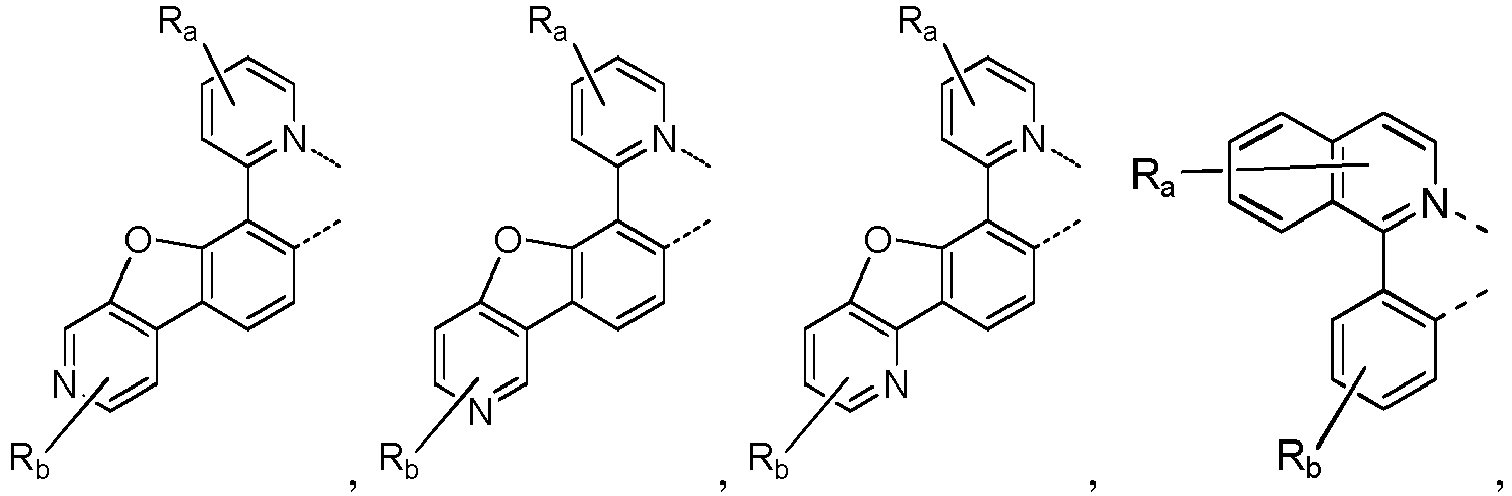
- a compound having a structure according to Formula II: wherein R 1 is selected from the group consisting of phenyl, biphenyl, terphenyl, tetraphenyl, pentaphenyl, pyridine, phenyl pyridine and pyridyl phenyl.
- L is selected from the group consisting of phenyl, pyridyl, biphenyl, terphenyl and a bond.
- R 4 is selected from the group consisting of phenyl, pyridyl, biphenyl, and terphenyl.
- R 5 is selected from the group consisting of phenyl, pyridyl, biphenyl, and terphenyl.
- R 2 and R 3 can be same or different, and independently selected from the group consisting of hydrogen, deuterium, non-fused aryl, non-fused heteroaryl and combinations thereof.
- Y 1 is N.
- the compound having a structure according to Formula II is selected from the group consisting of Compound 1 through Compound 161 and Compound 302 through 462, listed in the table below (Table 1), wherein Y 1 , R 1 , R 2 , R 3 , R 4 , R 5 and L are as defined and wherein C is Carbon, N is nitrogen, H is hydrogen, A 1 is A 2 is A 6 is Table 1 Cmpd Y 1 R 1 R 2 R 3 R 4 R 5 L 1 N A 1 H H A 1 A 1 Bond 2 N A 2 H H A 1 A 1 Bond 3 N A 3 H H H A 1 A 1 Bond 4 N A 4 H H A 1 A 1 Bond 5 N A 5 H H A 1 A 1 Bond 6 N A 6 H H A 1 A 1 Bond 7 N A 7 H H A 1 A 1 Bond 8 N A 1 A 1 H A 1 Bond 9 N A 2 A 1 H A 1 A 1 Bond 10 N A 3 A 1 H A 1 A 1 Bond 11 N A 4 A 1 H A 1 A 1 Bond 12 N A 5 A 1 H A 1 A 1 A 1 A
- the compound is selected from the group consisting of:
- a formulation comprising a compound of formula II is provided.
- a device comprising a organic light emitting device, further comprising: an anode; a cathode; an organic layer, disposed between the anode and the cathode, wherein the organic layer further comprising a compound having a structure according to Formula II as described herein.
- the device is an organic light-emitting device. In one embodiment, the device comprises a lighting panel. In one embodiment, the compound is selected from the group consisting of:
- the compound is selected from the compounds 1 through 161. In one embodiment, the compound is selected from the compounds 302 to 462. In one embodiment, the device is a consumer product. In one embodiment, the organic layer is an emissive layer and the compound of Formula II is a host. In one embodiment, the organic layer is a blocking layer and the compound having the formula II is a blocking material in the organic layer. In one embodiment, the organic layer is an electron transporting layer and the compound having the formula II is an electron transporting material in the organic layer.
- the exemplary compounds described herein comprise either carbazole or azacarbazole central unit.
- the compounds can be substituted directly at the 9-position with a triazine or a pyrimidine unit and with an aromatic unfused ring at the 1-position.
- the triazine linked to the 9-position of the carbazole can be further substituted by two similar aromatic rings or by two different substituents.
- the compounds described in this disclosure were found to have surprising and unexpected properties when used as electron-transporting hosts in the emissive layer of an organic light-emitting device.
- the present disclosure is based, at least in part, on the surprising and unexpected discovery that certain combinations of 1-arylated carbazole with either pyrimidine or triazine attached at the 9- position (nitrogen) of the carbazole contain two important parts, namely an electron rich part (carbazole) and an electron poor part (triazine).
- the substitution at the 1- position of the carbazole resulted in surprising and unexpected properties in order to provide steric hindrance which results twisting of the carbazole vs. triazine fragment. This substitution also enabled the compounds described herein to be completely amorphous and therefore they form higher quality films on the substrates.
- non-exemplary compounds that do not have these characteristic substitution show worse performance characteristics and lifetimes compared to their 1-substituted counterpart as described in the present disclosure.
- the type of substituents on the carbazole and triazine are very important for the improved properties. It was found that small pendant groups were very efficient in providing good performance characteristics.
- the number of substituents were optimized and/or selected based on the glass transition temperature (T G ) and deposition temperature (T D ), which are very important factors in obtaining stable devices.
- un-fused pendant groups that do not increase the rigidity of the material were used.
- the carbazole, as well as the triazine groups can be substituted with phenyl, biphenyl, terphenyl, and pyridine units.
- the known compounds that contain the triazine substituted carbazole usually contain other fused heterocycles like dibenzothiophene, dibenzofuran, or carbazole, which are unlike the compounds of the present disclosure comprising certain combinations of carbazole and triazine, both substituted with small and unfused pendant groups.
- Other dimer-like structures of such compounds are complicated to synthesize while not providing device improvement.
- the three pendant groups on the triazine moiety can be different.
- the exemplary functionalization is having one larger group on one end of the triazine and two other small units which are usually the same (phenyl).
- exemplary compounds described herein can be very efficient materials (host and blocking layer OLEDs for green and red emissive layer) and can be obtained by having three different functional groups on the triazine. This allows more freedom in terms of chemistry and possibility for the synthesis of new materials.
- the present disclosure is not limited to changing one third of the pendant groups on the triazine but all of them.
- the carbazole unit substituted with different triazine or pyrimidine units on the nitrogen combined with substitution with small pendant groups has great advantages as electron-transporting host.
- having a triazine unit on the carbazole moiety helps affording very good external quantum effiency (EQE) and power efficacy (PE) in the devices.
- EQE external quantum effiency
- PE power efficacy
- the addition of a pendant group at the 1-position on the carbazole lowers the driving voltage and also improves the lifetimes of the devices which are important problems to solve in the industry in order to have a viable host system and commercial development.
- the device may include an anode, a cathode, and an organic emissive layer disposed between the anode and the cathode.
- the organic emissive layer may include a host and a phosphorescent dopant.
- the materials described herein as useful for a particular layer in an organic light emitting device may be used in combination with a wide variety of other materials present in the device.
- emissive dopants disclosed herein may be used in conjunction with a wide variety of hosts, transport layers, blocking layers, injection layers, electrodes and other layers that may be present.
- the materials described or referred to below are non-limiting examples of materials that may be useful in combination with the compounds disclosed herein, and one of skill in the art can readily consult the literature to identify other materials that may be useful in combination.
- a hole injecting/transporting material to be used in the present invention is not particularly limited, and any compound may be used as long as the compound is typically used as a hole injecting/transporting material.
- the material include, but not limit to: a phthalocyanine or porphryin derivative; an aromatic amine derivative; an indolocarbazole derivative; a polymer containing fluorohydrocarbon; a polymer with conductivity dopants; a conducting polymer, such as PEDOT/PSS; a self-assembly monomer derived from compounds such as phosphonic acid and sliane derivatives; a metal oxide derivative, such as MoO x ; a p-type semiconducting organic compound, such as 1,4,5,8,9,12-Hexaazatriphenylenehexacarbonitrile; a metal complex, and a cross-linkable compounds.
- aromatic amine derivatives used in HIL or HTL include, but not limit to the following general structures:
- Each of Ar 1 to Ar 9 is selected from the group consisting aromatic hydrocarbon cyclic compounds such as benzene, biphenyl, triphenyl, triphenylene, naphthalene, anthracene, phenalene, phenanthrene, fluorene, pyrene, chrysene, perylene, azulene; group consisting aromatic heterocyclic compounds such as dibenzothiophene, dibenzofuran, dibenzoselenophene, furan, thiophene, benzofuran, benzothiophene, benzoselenophene, carbazole, indolocarbazole, pyridylindole, pyrrolodipyridine, pyrazole, imidazole, triazole, oxazole, thiazole, oxadiazole, oxatriazole, dioxazole, thiadiazole, pyridine, pyridazine, pyrim
- each Ar is further substituted by a substituent selected from the group consisting of hydrogen, deuterium, halide, alkyl, cycloalkyl, heteroalkyl, arylalkyl, alkoxy, aryloxy, amino, silyl, alkenyl, cycloalkenyl, heteroalkenyl, alkynyl, aryl, heteroaryl, acyl, carbonyl, carboxylic acids, ester, nitrile, isonitrile, sulfanyl, sulfinyl, sulfonyl, phosphino, and combinations thereof.
- a substituent selected from the group consisting of hydrogen, deuterium, halide, alkyl, cycloalkyl, heteroalkyl, arylalkyl, alkoxy, aryloxy, amino, silyl, alkenyl, cycloalkenyl, heteroalkenyl, alkynyl, aryl, heteroaryl, acy
- Ar 1 to Ar 9 is independently selected from the group consisting of:
- k is an integer from 1 to 20; X 101 to X 108 is C (including CH) or N; Z 101 is NAr 1 , O, or S; Ar 1 has the same group defined above.
- metal complexes used in HIL or HTL include, but not limit to the following general formula: wherein Met is a metal; (Y 101 -Y 102 ) is a bidentate ligand, Y 101 and Y 102 are independently selected from C, N, O, P, and S; L 101 is an another ligand; k' is an integer value from 1 to the maximum number of ligands that may be attached to the metal; and k'+k" is the maximum number of ligands that may be attached to the metal.
- (Y 101 -Y 102 ) is a 2-phenylpyridine derivative. In another aspect, (Y 101 -Y 102 ) is a carbene ligand. In another aspect, Met is selected from Ir, Pt, Os, and Zn. In a further aspect, the metal complex has a smallest oxidation potential in solution vs. Fc + /Fc couple less than about 0.6 V.
- the light emitting layer of the organic EL device of the present invention preferably contains at least a metal complex as light emitting material, and may contain a host material using the metal complex as a dopant material.
- the host material are not particularly limited, and any metal complexes or organic compounds may be used as long as the triplet energy of the host is larger than that of the dopant. While the Table below categorizes host materials as preferred for devices that emit various colors, any host material may be used with any dopant so long as the triplet criterion is satisfied.
- Examples of metal complexes used as host are preferred to have the following general formula: wherein Met is a metal; (Y 103 -Y 104 ) is a bidentate ligand, Y 103 and Y 104 are independently selected from C, N, O, P, and S; L 101 is an another ligand; k' is an integer value from 1 to the maximum number of ligands that may be attached to the metal; and k'+k" is the maximum number of ligands that may be attached to the metal.
- the metal complexes are: wherein (O-N) is a bidentate ligand, having metal coordinated to atoms O and N.
- Met is selected from Ir and Pt.
- (Y 103 -Y 104 ) is a carbene ligand.
- organic compounds used as host are selected from the group consisting aromatic hydrocarbon cyclic compounds such as benzene, biphenyl, triphenyl, triphenylene, naphthalene, anthracene, phenalene, phenanthrene, fluorene, pyrene, chrysene, perylene, azulene; group consisting aromatic heterocyclic compounds such as dibenzothiophene, dibenzofuran, dibenzoselenophene, furan, thiophene, benzofuran, benzothiophene, benzoselenophene, carbazole, indolocarbazole, pyridylindole, pyrrolodipyridine, pyrazole, imidazole, triazole, oxazole, thiazole, oxadiazole, oxatriazole, dioxazole, thiadiazole, pyridine, pyridazine, pyrimidine
- each group is further substituted by a substituent selected from the group consisting of hydrogen, deuterium, halide, alkyl, cycloalkyl, heteroalkyl, arylalkyl, alkoxy, aryloxy, amino, silyl, alkenyl, cycloalkenyl, heteroalkenyl, alkynyl, aryl, heteroaryl, acyl, carbonyl, carboxylic acids, ester, nitrile, isonitrile, sulfanyl, sulfinyl, sulfonyl, phosphino, and combinations thereof.
- a substituent selected from the group consisting of hydrogen, deuterium, halide, alkyl, cycloalkyl, heteroalkyl, arylalkyl, alkoxy, aryloxy, amino, silyl, alkenyl, cycloalkenyl, heteroalkenyl, alkynyl, aryl, heteroaryl, acy
- host compound contains at least one of the following groups in the molecule: wherein R 101 to R 107 is independently selected from the group consisting of hydrogen, deuterium, halide, alkyl, cycloalkyl, heteroalkyl, arylalkyl, alkoxy, aryloxy, amino, silyl, alkenyl, cycloalkenyl, heteroalkenyl, alkynyl, aryl, heteroaryl, acyl, carbonyl, carboxylic acids, ester, nitrile, isonitrile, sulfanyl, sulfinyl, sulfonyl, phosphino, and combinations thereof, when it is aryl or heteroaryl, it has the similar definition as Ar's mentioned above.
- k is an integer from 1 to 20; k'" is an integer from 0 to 20.
- X 101 to X 108 is selected from C (including CH) or N.
- Z 101 and Z 102 is selected from NR
- a hole blocking layer may be used to reduce the number of holes and/or excitons that leave the emissive layer.
- the presence of such a blocking layer in a device may result in substantially higher efficiencies as compared to a similar device lacking a blocking layer.
- a blocking layer may be used to confine emission to a desired region of an OLED.
- compound used in HBL contains the same molecule or the same functional groups used as host described above.
- compound used in HBL contains at least one of the following groups in the molecule:
- k is an integer from 1 to 20; L 101 is an another ligand, k' is an integer from 1 to 3.
- Electron transport layer may include a material capable of transporting electrons. Electron transport layer may be intrinsic (undoped), or doped. Doping may be used to enhance conductivity. Examples of the ETL material are not particularly limited, and any metal complexes or organic compounds may be used as long as they are typically used to transport electrons.
- compound used in ETL contains at least one of the following groups in the molecule: wherein R 101 is selected from the group consisting of hydrogen, deuterium, halide, alkyl, cycloalkyl, heteroalkyl, arylalkyl, alkoxy, aryloxy, amino, silyl, alkenyl, cycloalkenyl, heteroalkenyl, alkynyl, aryl, heteroaryl, acyl, carbonyl, carboxylic acids, ester, nitrile, isonitrile, sulfanyl, sulfinyl, sulfonyl, phosphino, and combinations thereof, when it is aryl or heteroaryl, it has the similar definition as Ar's mentioned above.
- Ar 1 to Ar 3 has the similar definition as Ar's mentioned above.
- k is an integer from 1 to 20.
- X 101 to X 108 is selected from C (including CH) or N.
- the metal complexes used in ETL contains, but not limit to the following general formula:
- (O-N) or (N-N) is a bidentate ligand, having metal coordinated to atoms O, N or N, N; L 101 is another ligand; k' is an integer value from 1 to the maximum number of ligands that may be attached to the metal.
- the hydrogen atoms can be partially or fully deuterated.
- any specifically listed substituent such as, without limitation, methyl, phenyl, pyridyl, etc. encompasses undeuterated, partially deuterated, and fully deuterated versions thereof.
- classes of substituents such as, without limitation, alkyl, aryl, cycloalkyl, heteroaryl, etc. also encompass undeuterated, partially deuterated, and fully deuterated versions thereof.
- hole injection materials In addition to and / or in combination with the materials disclosed herein, many hole injection materials, hole transporting materials, host materials, dopant materials, exiton/hole blocking layer materials, electron transporting and electron injecting materials may be used in an OLED.
- Non-limiting examples of the materials that may be used in an OLED in combination with materials disclosed herein are listed in Table 5 below. Table 5 lists non-limiting classes of materials, non-limiting examples of compounds for each class, and references that disclose the materials. TABLE 5 MATERIAL EXAMPLES OF MATERIAL PUBLICATIONS Hole injection materials Phthalocyanine and porphryin compounds Appl. Phys. Lett. 69, 2160 (1996 ) Starburst triarylamines J. Lumin.
- the precipitate was collected by filtration, solubilized in DCM and coated on Celite to purify by column chromatography on silica gel eluted with 25% of dichloromethane (DCM) in heptanes. Because of some solubility issues, the separation was not efficient. After evaporating of the solvent, the solid was triturated in EtOH 2 times to afford 1-bromo-9-(4,6-diphenyl-1,3,5-triazin-2-yl)-9H-carbazole (1.5 g, 77% yield) as a white powder.
- DCM dichloromethane
- the aqueous layer was washed two times with ethyl acetate.
- the combined organic layers were washed with brine and water and dried with sodium sulfate.
- the crude material was coated on celite and purified by column chromatography with 15-30% gradient mixture of DCM in heptanes. After evaporation of the solvent, the solid was triturated with EtOH and then the collected solid was recrystallized from heptanes and toluene.
- the product was extracted with DCM and washed with brine and water.
- the white solid was triturated from methanol one time and one more time using heptanes.
- the material (5.79 g, 89% yield) was approximately 90% pure and was used in the next step without further purification.
- the mixture was degassed by bubbling nitrogen, followed by addition of Pd 2 (dba) 3 (0.662 g, 0.723 mmol) and dicyclohexyl(2',6'-dimethoxy-[1,1'-biphenyl]-2-yl)phosphine (SPhOS) (1.187 g, 2.89 mmol).
- Pd 2 (dba) 3 0.662 g, 0.723 mmol
- SPhOS dicyclohexyl(2',6'-dimethoxy-[1,1'-biphenyl]-2-yl)phosphine
- the powder was solubilized in DCM and i -propanol was added.
- the DCM was slowly evaporated out of the mixture to obtain precipitation of the target with better purity (99.6%).
- the target material, Compound 30, was purified using column chromatography (30% DCM in Heptanes) and 1.2 g (26% yield).
- the mixture was degassed by bubbling nitrogen, then it washeated to reflux overnight. After completion of the reaction, the mixture partitioned between ethyl acetate and water. The aqueous layer was washed 3 times with ethyl acetate and the combined organic layers were washed with brine and water.
- the crude compound was purified by column chromatography on silica gel, eluted with hexane/DCM 1/1 (v/v) mixture. The target compound was obtained as a white solid (7.4 g, 75 % yield).
- All example devices were fabricated by high vacuum ( ⁇ 10 -7 Torr) thermal evaporation.
- the anode electrode is 1200 ⁇ of indium tin oxide (ITO).
- the cathode consisted of 10 ⁇ of LiF followed by 1,000 ⁇ of Al. All devices are encapsulated with a glass lid sealed with an epoxy resin in a nitrogen glove box ( ⁇ 1 ppm of H 2 O and O 2 ) immediately after fabrication, and a moisture getter was incorporated inside the package.
- the organic stack of the OLED device consisted of sequentially from the ITO surface, 100 ⁇ of HAT-CN as the hole injection layer (HIL), 400 ⁇ of NPD as the hole transporting layer (HTL), 300 ⁇ of the emissive layer (EML) which contains the compound of Formula 1, Compound SD, and Compound D, 550 ⁇ of AlQ 3 as the electron transporting layer (ETL) and 10 ⁇ of LiF as the electron injection layer (EIL).
- HIL hole injection layer
- HTL hole transporting layer
- EML emissive layer
- ETL electron transporting layer
- HIL HTL EML 300 ⁇ , doping %) BL ETL
- Table 8 is a summary of the device data.
- the luminous efficiency (LE), external quantum efficiency (EQE) and power efficiency (PE) were measured at 1000 nits, while the lifetime (LT 95% ) was defined as the time required for the device to decay to 95% of its initial luminance under a constant current density of 40 mA/cm 2 .
- Compounds such as Comparative Compound 1, which does not contain any substitution at the 1- position of the carbazole does not perform as well as Compound 2 which combines the triazine substitution on the nitrogen of the carbazole and substitution at the 1- position of the carbazole.
- Comparative Compound 1 which does not contain any substitution at the 1- position of the carbazole does not perform as well as Compound 2 which combines the triazine substitution on the nitrogen of the carbazole and substitution at the 1- position of the carbazole.
- Compound 2 which combines the triazine substitution on the nitrogen of the carbazole and substitution at the 1- position of the carbazole.
- Table 2 when the device contains Com
- the luminous efficacy (LE), external quantum efficiency (EQE), power efficacy (PE) and operational lifetime (LT 95% ) are all improved compared to the devices which contain Comparative Compound 1 as the host.
- the performances are also improved when the blocking layer (BL) is Compound 2 compared to BAlQ.
- the best device obtained with Compound 2 (in relative numbers - compared to Comparative Compound 1) in this study showed a x value from the CIE of 0.661, a driving voltage of 0.78, an LE of 1.2, an EQE of 1.2, a PE of 1.6, and finally an LT 95% (measured at 1000 nits) of more than 4 times than the lifetime of the comparative example.
Landscapes
- Chemical & Material Sciences (AREA)
- Organic Chemistry (AREA)
- Physics & Mathematics (AREA)
- Engineering & Computer Science (AREA)
- Materials Engineering (AREA)
- Spectroscopy & Molecular Physics (AREA)
- Optics & Photonics (AREA)
- Electroluminescent Light Sources (AREA)
- Plural Heterocyclic Compounds (AREA)
- Pharmaceuticals Containing Other Organic And Inorganic Compounds (AREA)
- Detergent Compositions (AREA)
- Measuring Or Testing Involving Enzymes Or Micro-Organisms (AREA)
Claims (10)
- Eine Verbindung mit einer Struktur gemäß Formel II:
 wobei R1 ausgewählt ist aus der Gruppe bestehend aus Phenyl, Biphenyl, Terphenyl, Tetraphenyl, Pentaphenyl, Pyridin, Phenylpyridin und Pyridylphenyl;wobei R4 ausgewählt ist aus der Gruppe bestehend aus Phenyl, Pyridyl, Biphenyl, und Terphenyl;wobei R5 ausgewählt ist aus der Gruppe bestehend aus Phenyl, Pyridyl, Biphenyl, und Terphenyl;wobei R2 und R3 gleich oder verschieden sein können und unabhängig ausgewählt sind aus der Gruppe bestehend aus Wasserstoff, Deuterium, nicht fusioniertes Aryl, nicht fusioniertes Heteroaryl und deren Kombinationen;wobei L ausgewählt ist aus der Gruppe bestehend aus Phenyl, Pyridyl, Biphenyl, Terphenyl und einer Bindung; undwobei Y1 gleich N ist.
 - Die Verbindung nach Anspruch 1, wobei die Verbindung mit einer Struktur gemäß Formel II ausgewählt ist aus der Gruppe bestehend aus Verbindung 1 bis Verbindung 161 und Verbindung 302 bis 462, wie in der unten angegebenen Tabelle aufgeführt, wobei Y1, R1, R2, R3, R4, R5 und L wie definiert sind und wobei C Kohlenstoff ist, N ist Stickstoff, H ist Wasserstoff, A1 ist


Verbindung Y1 R1 R2 R3 R4 R5 L 1 N A1 H H A1 A1 Bindung 2 N A2 H H A1 A1 Bindung 3 N A3 H H A1 A1 Bindung 4 N A4 H H A1 A1 Bindung 5 N A5 H H A1 A1 Bindung 6 N A6 H H A1 A1 Bindung 7 N A7 H H A1 A1 Bindung 8 N A1 A1 H A1 A1 Bindung 9 N A2 A1 H A1 A1 Bindung 10 N A3 A1 H A1 A1 Bindung 11 N A4 A1 H A1 A1 Bindung 12 N A5 A1 H A1 A1 Bindung 13 N A6 A1 H A1 A1 Bindung 14 N A7 A1 H A1 A1 Bindung 15 N A1 H A1 A1 A1 Bindung 16 N A2 H A1 A1 A1 Bindung 17 N A3 H A1 A1 A1 Bindung 18 N A4 H A1 A1 A1 Bindung 19 N A5 H A1 A1 A1 Bindung 20 N A6 H A1 A1 A1 Bindung 21 N A7 H A1 A1 A1 Bindung 22 N A1 A1 A1 A1 A1 Bindung 23 N A2 A1 A1 A1 A1 Bindung 24 N A3 A1 A1 A1 A1 Bindung 25 N A4 A1 A1 A1 A1 Bindung 26 N A5 A1 A1 A1 A1 Bindung 27 N A6 A1 A1 A1 A1 Bindung 28 N A7 A1 A1 A1 A1 Bindung 29 N A1 H H A2 A1 Bindung 30 N A2 H H A2 A1 Bindung 31 N A3 H H A2 A1 Bindung 32 N A4 H H A2 A1 Bindung 33 N A5 H H A2 A1 Bindung 34 N A6 H H A2 A1 Bindung 35 N A7 H H A2 A1 Bindung 36 N A1 A1 H A2 A1 Bindung 37 N A2 A1 H A2 A1 Bindung 38 N A3 A1 H A2 A1 Bindung 39 N A4 A1 H A2 A1 Bindung 40 N A5 A1 H A2 A1 Bindung 41 N A6 A1 H A2 A1 Bindung 42 N A7 A1 H A2 A1 Bindung 43 N A1 H A1 A2 A1 Bindung 44 N A2 H A1 A2 A1 Bindung 45 N A3 H A1 A2 A1 Bindung 46 N A4 H A1 A2 A1 Bindung 47 N A5 H A1 A2 A1 Bindung 48 N A6 H A1 A2 A1 Bindung 49 N A7 H A1 A2 A1 Bindung 50 N A1 A1 A1 A2 A1 Bindung 51 N A2 A1 A1 A2 A1 Bindung 52 N A3 A1 A1 A2 A1 Bindung 53 N A4 A1 A1 A2 A1 Bindung 54 N A5 A1 A1 A2 A1 Bindung 55 N A6 A1 A1 A2 A1 Bindung 56 N A7 A1 A1 A2 A1 Bindung 57 N A1 H H A2 A2 Bindung 58 N A2 H H A2 A2 Bindung 59 N A3 H H A2 A2 Bindung 60 N A4 H H A2 A2 Bindung 61 N A5 H H A2 A2 Bindung 62 N A6 H H A2 A2 Bindung 63 N A7 H H A2 A2 Bindung 64 N A1 A1 H A2 A2 Bindung 65 N A2 A1 H A2 A2 Bindung 66 N A3 A1 H A2 A2 Bindung 67 N A4 A1 H A2 A2 Bindung 68 N A5 A1 H A2 A2 Bindung 69 N A6 A1 H A2 A2 Bindung 70 N A7 A1 H A2 A2 Bindung 71 N A1 H A1 A2 A2 Bindung 72 N A2 H A1 A2 A2 Bindung 73 N A3 H A1 A2 A2 Bindung 74 N A4 H A1 A2 A2 Bindung 75 N A5 H A1 A2 A2 Bindung 76 N A6 H A1 A2 A2 Bindung 77 N A7 H A1 A2 A2 Bindung 78 N A1 A1 A1 A2 A2 Bindung 79 N A2 A1 A1 A2 A2 Bindung 80 N A3 A1 A1 A2 A2 Bindung 81 N A4 A1 A1 A2 A2 Bindung 82 N A5 A1 A1 A2 A2 Bindung 83 N A6 A1 A1 A2 A2 Bindung 84 N A7 A1 A1 A2 A2 Bindung 85 N A1 H H A3 A1 Bindung 86 N A2 H H A3 A1 Bindung 87 N A3 H H A3 A1 Bindung 88 N A4 H H A3 A1 Bindung 89 N A5 H H A3 A1 Bindung 90 N A6 H H A3 A1 Bindung 91 N A7 H H A3 A1 Bindung 92 N A1 A1 H A3 A1 Bindung 93 N A2 A1 H A3 A1 Bindung 94 N A3 A1 H A3 A1 Bindung 95 N A4 A1 H A3 A1 Bindung 96 N A5 A1 H A3 A1 Bindung 97 N A6 A1 H A3 A1 Bindung 98 N A7 A1 H A3 A1 Bindung 99 N A1 H A1 A3 A1 Bindung 100 N A2 H A1 A3 A1 Bindung 101 N A3 H A1 A3 A1 Bindung 102 N A4 H A1 A3 A1 Bindung 103 N A5 H A1 A3 A1 Bindung 104 N A6 H A1 A3 A1 Bindung 105 N A7 H A1 A3 A1 Bindung 106 N A1 A1 A1 A3 A1 Bindung 107 N A2 A1 A1 A3 A1 Bindung 108 N A3 A1 A1 A3 A1 Bindung 109 N A4 A1 A1 A3 A1 Bindung 110 N A5 A1 A1 A3 A1 Bindung 111 N A6 A1 A1 A3 A1 Bindung 112 N A7 A1 A1 A3 A1 Bindung 113 N A1 H H A3 A3 Bindung 114 N A2 H H A3 A3 Bindung 115 N A3 H H A3 A3 Bindung 116 N A4 H H A3 A3 Bindung 117 N A5 H H A3 A3 Bindung 118 N A6 H H A3 A3 Bindung 119 N A7 H H A3 A3 Bindung 120 N A1 A1 H A3 A3 Bindung 121 N A2 A1 H A3 A3 Bindung 122 N A3 A1 H A3 A3 Bindung 123 N A4 A1 H A3 A3 Bindung 124 N A5 A1 H A3 A3 Bindung 125 N A6 A1 H A3 A3 Bindung 126 N A7 A1 H A3 A3 Bindung 127 N A1 H A1 A3 A3 Bindung 128 N A2 H A1 A3 A3 Bindung 129 N A3 H A1 A3 A3 Bindung 130 N A4 H A1 A3 A3 Bindung 131 N A5 H A1 A3 A3 Bindung 132 N A6 H A1 A3 A3 Bindung 133 N A7 H A1 A3 A3 Bindung 134 N A1 A1 A1 A3 A3 Bindung 135 N A2 A1 A1 A3 A3 Bindung 136 N A3 A1 A1 A3 A3 Bindung 137 N A4 A1 A1 A3 A3 Bindung 138 N A5 A1 A1 A3 A3 Bindung 139 N A6 A1 A1 A3 A3 Bindung 140 N A7 A1 A1 A3 A3 Bindung 141 N A1 A2 H A1 A1 Bindung 142 N A2 A2 H A1 A1 Bindung 143 N A3 A2 H A1 A1 Bindung 144 N A4 A2 H A1 A1 Bindung 145 N A5 A2 H A1 A1 Bindung 146 N A6 A2 H A1 A1 Bindung 147 N A7 A2 H A1 A1 Bindung 148 N A1 A2 H A2 A1 Bindung 149 N A2 A2 H A2 A1 Bindung 150 N A3 A2 H A2 A1 Bindung 151 N A4 A2 H A2 A1 Bindung 152 N A5 A2 H A2 A1 Bindung 153 N A6 A2 H A2 A1 Bindung 154 N A7 A2 H A2 A1 Bindung 155 N A1 A2 H A2 A2 Bindung 156 N A2 A2 H A2 A2 Bindung 157 N A3 A2 H A2 A2 Bindung 158 N A4 A2 H A2 A2 Bindung 159 N A5 A2 H A2 A2 Bindung 160 N A6 A2 H A2 A2 Bindung 161 N A7 A2 H A2 A2 Bindung 302 N A1 H H A1 A1 A8 303 N A2 H H A1 A1 A8 304 N A3 H H A1 A1 A8 305 N A4 H H A1 A1 A8 306 N A5 H H A1 A1 A8 307 N A6 H H A1 A1 A8 308 N A7 H H A1 A1 A8 309 N A1 A1 H A1 A1 A8 310 N A2 A1 H A1 A1 A8 311 N A3 A1 H A1 A1 A8 312 N A4 A1 H A1 A1 A8 313 N A5 A1 H A1 A1 A8 314 N A6 A1 H A1 A1 A8 315 N A7 A1 H A1 A1 A8 316 N A1 H A1 A1 A1 A8 317 N A2 H A1 A1 A1 A8 318 N A3 H A1 A1 A1 A8 319 N A4 H A1 A1 A1 A8 320 N A5 H A1 A1 A1 A8 321 N A6 H A1 A1 A1 A8 322 N A7 H A1 A1 A1 A8 323 N A1 A1 A1 A1 A1 A8 324 N A2 A1 A1 A1 A1 A8 325 N A3 A1 A1 A1 A1 A8 326 N A4 A1 A1 A1 A1 A8 327 N A5 A1 A1 A1 A1 A8 328 N A6 A1 A1 A1 A1 A8 329 N A7 A1 A1 A1 A1 A8 330 N A1 H H A2 A1 A8 331 N A2 H H A2 A1 A8 332 N A3 H H A2 A1 A8 333 N A4 H H A2 A1 A8 334 N A5 H H A2 A1 A8 335 N A6 H H A2 A1 A8 336 N A7 H H A2 A1 A8 337 N A1 A1 H A2 A1 A8 338 N A2 A1 H A2 A1 A8 339 N A3 A1 H A2 A1 A8 340 N A4 A1 H A2 A1 A8 341 N A5 A1 H A2 A1 A8 342 N A6 A1 H A2 A1 A8 343 N A7 A1 H A2 A1 A8 344 N A1 H A1 A2 A1 A8 345 N A2 H A1 A2 A1 A8 346 N A3 H A1 A2 A1 A8 347 N A4 H A1 A2 A1 A8 348 N A5 H A1 A2 A1 A8 349 N A6 H A1 A2 A1 A8 350 N A7 H A1 A2 A1 A8 351 N A1 A1 A1 A2 A1 A8 352 N A2 A1 A1 A2 A1 A8 353 N A3 A1 A1 A2 A1 A8 354 N A4 A1 A1 A2 A1 A8 355 N A5 A1 A1 A2 A1 A8 356 N A6 A1 A1 A2 A1 A8 357 N A7 A1 A1 A2 A1 A8 358 N A1 H H A2 A2 A8 359 N A2 H H A2 A2 A8 360 N A3 H H A2 A2 A8 361 N A4 H H A2 A2 A8 362 N A5 H H A2 A2 A8 363 N A6 H H A2 A2 A8 364 N A7 H H A2 A2 A8 365 N A1 A1 H A2 A2 A8 366 N A2 A1 H A2 A2 A8 367 N A3 A1 H A2 A2 A8 368 N A4 A1 H A2 A2 A8 369 N A5 A1 H A2 A2 A8 370 N A6 A1 H A2 A2 A8 371 N A7 A1 H A2 A2 A8 372 N A1 H A1 A2 A2 A8 373 N A2 H A1 A2 A2 A8 374 N A3 H A1 A2 A2 A8 375 N A4 H A1 A2 A2 A8 376 N A5 H A1 A2 A2 A8 377 N A6 H A1 A2 A2 A8 378 N A7 H A1 A2 A2 A8 379 N A1 A1 A1 A2 A2 A8 380 N A2 A1 A1 A2 A2 A8 381 N A3 A1 A1 A2 A2 A8 382 N A4 A1 A1 A2 A2 A8 383 N A5 A1 A1 A2 A2 A8 384 N A6 A1 A1 A2 A2 A8 385 N A7 A1 A1 A2 A2 A8 386 N A1 H H A3 A1 A8 387 N A2 H H A3 A1 A8 388 N A3 H H A3 A1 A8 389 N A4 H H A3 A1 A8 390 N A5 H H A3 A1 A8 391 N A6 H H A3 A1 A8 392 N A7 H H A3 A1 A8 393 N A1 A1 H A3 A1 A8 394 N A2 A1 H A3 A1 A8 395 N A3 A1 H A3 A1 A8 396 N A4 A1 H A3 A1 A8 397 N A5 A1 H A3 A1 A8 398 N A6 A1 H A3 A1 A8 399 N A7 A1 H A3 A1 A8 400 N A1 H A1 A3 A1 A8 401 N A2 H A1 A3 A1 A8 402 N A3 H A1 A3 A1 A8 403 N A4 H A1 A3 A1 A8 404 N A5 H A1 A3 A1 A8 405 N A6 H A1 A3 A1 A8 406 N A7 H A1 A3 A1 A8 407 N A1 A1 A1 A3 A1 A8 408 N A2 A1 A1 A3 A1 A8 409 N A3 A1 A1 A3 A1 A8 410 N A4 A1 A1 A3 A1 A8 411 N A5 A1 A1 A3 A1 A8 412 N A6 A1 A1 A3 A1 A8 413 N A7 A1 A1 A3 A1 A8 414 N A1 H H A3 A3 A8 415 N A2 H H A3 A3 A8 416 N A3 H H A3 A3 A8 417 N A4 H H A3 A3 A8 418 N A5 H H A3 A3 A8 419 N A6 H H A3 A3 A8 420 N A7 H H A3 A3 A8 421 N A1 A1 H A3 A3 A8 422 N A2 A1 H A3 A3 A8 423 N A3 A1 H A3 A3 A8 424 N A4 A1 H A3 A3 A8 425 N A5 A1 H A3 A3 A8 426 N A6 A1 H A3 A3 A8 427 N A7 A1 H A3 A3 A8 428 N A1 H A1 A3 A3 A8 429 N A2 H A1 A3 A3 A8 430 N A3 H A1 A3 A3 A8 431 N A4 H A1 A3 A3 A8 432 N A5 H A1 A3 A3 A8 433 N A6 H A1 A3 A3 A8 434 N A7 H A1 A3 A3 A8 435 N A1 A1 A1 A3 A3 A8 436 N A2 A1 A1 A3 A3 A8 437 N A3 A1 A1 A3 A3 A8 438 N A4 A1 A1 A3 A3 A8 439 N A5 A1 A1 A3 A3 A8 440 N A6 A1 A1 A3 A3 A8 441 N A7 A1 A1 A3 A3 A8 442 N A1 A2 H A1 A1 A8 443 N A2 A2 H A1 A1 A8 444 N A3 A2 H A1 A1 A8 445 N A4 A2 H A1 A1 A8 446 N A5 A2 H A1 A1 A8 447 N A6 A2 H A1 A1 A8 448 N A7 A2 H A1 A1 A8 449 N A1 A2 H A2 A1 A8 450 N A2 A2 H A2 A1 A8 451 N A3 A2 H A2 A1 A8 452 N A4 A2 H A2 A1 A8 453 N A5 A2 H A2 A1 A8 454 N A6 A2 H A2 A1 A8 455 N A7 A2 H A2 A1 A8 456 N A1 A2 H A2 A2 A8 457 N A2 A2 H A2 A2 A8 458 N A3 A2 H A2 A2 A8 459 N A4 A2 H A2 A2 A8 460 N A5 A2 H A2 A2 A8 461 N A6 A2 H A2 A2 A8 462 N A7 A2 H A2 A2 A8 - Die Verbindung nach Anspruch 1, wobei die Verbindung ausgewählt ist aus der Gruppe bestehend aus:


- Eine Formulierung umfassend eine Verbindung nach Anspruch 1.
- Eine Vorrichtung umfassend eine organische Licht emittierende Vorrichtung, die organische Licht emittierende Vorrichtung umfassend:eine Anode;eine Kathode;eine organische Schicht, angeordnet zwischen der Anode und der Kathode, wobei die organische Schicht ferner umfasst eine Verbindung wie in Anspruch 1 definiert.
- Die Vorrichtung nach Anspruch 5, wobei die Vorrichtung eine organische Licht emittierende Vorrichtung ist.
- Die Vorrichtung nach Anspruch 5, wobei die Verbindung ausgewählt ist aus der Gruppe bestehend aus:


- Die Vorrichtung nach Anspruch 5, wobei die Vorrichtung ein Konsumentenprodukt ist.
- Die Vorrichtung nach Anspruch 5, wobei(a) die organische Schicht eine emittierende Schicht und die Verbindung gemäß Formel II ein Wirt ist;
oder(b) die organische Schicht eine Blockingschicht ist und die Verbindung mit der Formel II ein Blockiermaterial in der organischen Schicht ist;
oder(c) die organische Schicht ist eine Elektronen transportierende Schicht und die Verbindung mit der Formel II ist ein Elektronen transportierendes Material in der organischen Schicht. - Die Vorrichtung nach Anspruch 5, ferner umfassend ein erstes Dotierstoffmaterial, das ein emittierender Dotierstoff ist, umfassend einen Übergangsmetallkomplex mit mindestens einem Liganden oder Teil des Liganden wenn der Ligand mehr als Bidentat ist, ausgewählt aus der Gruppe bestehend aus:


 wobei Ra, Rb, und Rc für mono-, di-, tri- oder tetra-Substitutionen stehen können;Ra, Rb, und Rc sind unabhängig ausgewählt aus der Gruppe bestehend aus Wasserstoff, Deuterium, Halogen, Alkyl, Cycloalkyl, Heteroalkyl, Arylalkyl, Alkoxy, Aryloxy, Amino, Silyl, Alkenyl, Cycloalkenyl, Heteroalkenyl, Alkinyl, Aryl, Heteroaryl, Acyl, Carbonyl, Carbonsäuren, Ester, Nitril, Isonitril, Sulfanyl, Sulfinyl, Sulfonyl, Phosphino, und deren Kombinationen; undzwei benachbarte Substituenten von Ra, Rb, und Rc gegebenenfalls verknüpft sind um einen fusionierten Ring oder einen multidentaten Liganden zu bilden.
Applications Claiming Priority (2)
| Application Number | Priority Date | Filing Date | Title |
|---|---|---|---|
| US13/930,997 US9673401B2 (en) | 2013-06-28 | 2013-06-28 | Organic electroluminescent materials and devices |
| EP14173684.3A EP2818468B1 (de) | 2013-06-28 | 2014-06-24 | Wirtsmaterialien für Pholeds |
Related Parent Applications (1)
| Application Number | Title | Priority Date | Filing Date |
|---|---|---|---|
| EP14173684.3A Division EP2818468B1 (de) | 2013-06-28 | 2014-06-24 | Wirtsmaterialien für Pholeds |
Publications (2)
| Publication Number | Publication Date |
|---|---|
| EP3309155A1 EP3309155A1 (de) | 2018-04-18 |
| EP3309155B1 true EP3309155B1 (de) | 2020-12-09 |
Family
ID=50979684
Family Applications (2)
| Application Number | Title | Priority Date | Filing Date |
|---|---|---|---|
| EP17198124.4A Active EP3309155B1 (de) | 2013-06-28 | 2014-06-24 | Host-materialien für pholeds |
| EP14173684.3A Active EP2818468B1 (de) | 2013-06-28 | 2014-06-24 | Wirtsmaterialien für Pholeds |
Family Applications After (1)
| Application Number | Title | Priority Date | Filing Date |
|---|---|---|---|
| EP14173684.3A Active EP2818468B1 (de) | 2013-06-28 | 2014-06-24 | Wirtsmaterialien für Pholeds |
Country Status (5)
| Country | Link |
|---|---|
| US (1) | US9673401B2 (de) |
| EP (2) | EP3309155B1 (de) |
| JP (2) | JP6385152B2 (de) |
| KR (2) | KR20150002466A (de) |
| CN (2) | CN104250244B (de) |
Families Citing this family (25)
| Publication number | Priority date | Publication date | Assignee | Title |
|---|---|---|---|---|
| US9673401B2 (en) * | 2013-06-28 | 2017-06-06 | Universal Display Corporation | Organic electroluminescent materials and devices |
| US10074806B2 (en) | 2013-08-20 | 2018-09-11 | Universal Display Corporation | Organic electroluminescent materials and devices |
| KR20150108330A (ko) * | 2014-03-17 | 2015-09-25 | 롬엔드하스전자재료코리아유한회사 | 전자 버퍼 재료 및 이를 포함하는 유기 전계 발광 소자 |
| WO2015142036A1 (en) * | 2014-03-17 | 2015-09-24 | Rohm And Haas Electronic Materials Korea Ltd. | Electron buffering material and organic electroluminescent device comprising the same |
| KR101765027B1 (ko) * | 2014-04-11 | 2017-08-03 | 메르크 파텐트 게엠베하 | 유기 전계발광 소자용 물질 |
| KR101706659B1 (ko) * | 2014-05-22 | 2017-02-17 | (주)아이티켐 | 신규한 유기발광화합물 및 이를 이용한 유기발광소자 |
| CN104045595A (zh) * | 2014-06-25 | 2014-09-17 | 北京绿人科技有限责任公司 | 一种有机化合物及其使用该有机化合物的电致发光器件 |
| KR101818582B1 (ko) * | 2014-11-04 | 2018-01-15 | 삼성에스디아이 주식회사 | 유기 광전자 소자용 화합물, 이를 포함하는 유기 광전자 소자 및 표시장치 |
| US10804473B2 (en) * | 2015-05-21 | 2020-10-13 | Lg Chem, Ltd. | Electron transport materials for electronic applications |
| JP6641948B2 (ja) * | 2015-12-04 | 2020-02-05 | コニカミノルタ株式会社 | 有機エレクトロルミネッセンス素子、表示装置、照明装置及び芳香族複素環誘導体 |
| JP6641947B2 (ja) * | 2015-12-04 | 2020-02-05 | コニカミノルタ株式会社 | 有機エレクトロルミネッセンス素子、表示装置、照明装置及び芳香族複素環誘導体 |
| GB2549246A (en) * | 2015-12-15 | 2017-10-18 | Cambridge Display Tech Ltd | Light-emitting Compound |
| JP7023452B2 (ja) * | 2016-06-17 | 2022-02-22 | 株式会社Kyulux | 発光材料、有機発光素子および化合物 |
| JP2020113557A (ja) * | 2017-03-28 | 2020-07-27 | 保土谷化学工業株式会社 | アザカルバゾール構造を有する化合物および有機エレクトロルミネッセンス素子 |
| CN109111433A (zh) * | 2017-06-22 | 2019-01-01 | 北京鼎材科技有限公司 | 一种有机电致发光化合物及其用途和有机电致发光器件 |
| US11706977B2 (en) | 2018-01-11 | 2023-07-18 | Samsung Electronics Co., Ltd. | Heterocyclic compound, composition including the same, and organic light-emitting device including the heterocyclic compound |
| WO2019235857A1 (ko) * | 2018-06-08 | 2019-12-12 | 삼성에스디아이 주식회사 | 유기 광전자 소자용 화합물, 유기 광전자 소자용 조성물, 유기 광전자 소자 및 표시 장치 |
| KR102756353B1 (ko) * | 2018-12-21 | 2025-01-20 | 덕산네오룩스 주식회사 | 유기전기 소자용 화합물, 이를 이용한 유기전기소자 및 그 전자 장치 |
| CN111620853B (zh) | 2019-02-28 | 2023-07-28 | 北京夏禾科技有限公司 | 有机电致发光材料及其器件 |
| KR102703933B1 (ko) * | 2019-04-10 | 2024-09-06 | 솔루스첨단소재 주식회사 | 유기 화합물 및 이를 포함하는 유기 전계 발광 소자 |
| CN110294755A (zh) * | 2019-04-30 | 2019-10-01 | 北京诚志永华显示科技有限公司 | 有机电致发光化合物及其应用 |
| CN110483500A (zh) * | 2019-07-10 | 2019-11-22 | 南京友斯贝特光电材料有限公司 | 一种oled主体材料及其制备方法与oled器件 |
| KR102495275B1 (ko) * | 2019-10-02 | 2023-02-01 | 삼성에스디아이 주식회사 | 유기 광전자 소자용 화합물, 유기 광전자 소자 및 표시 장치 |
| KR102869108B1 (ko) * | 2019-10-24 | 2025-10-14 | 듀폰스페셜티머터리얼스코리아 유한회사 | 복수 종의 호스트 재료 및 이를 포함하는 유기 전계 발광 소자 |
| US20240038096A1 (en) * | 2022-07-26 | 2024-02-01 | Triad National Security, Llc | Method and system for simulating handling of radioactive material safety during training |
Family Cites Families (148)
| Publication number | Priority date | Publication date | Assignee | Title |
|---|---|---|---|---|
| US4769292A (en) | 1987-03-02 | 1988-09-06 | Eastman Kodak Company | Electroluminescent device with modified thin film luminescent zone |
| GB8909011D0 (en) | 1989-04-20 | 1989-06-07 | Friend Richard H | Electroluminescent devices |
| US5061569A (en) | 1990-07-26 | 1991-10-29 | Eastman Kodak Company | Electroluminescent device with organic electroluminescent medium |
| EP0650955B1 (de) | 1993-11-01 | 1998-08-19 | Hodogaya Chemical Co., Ltd. | Aminverbindung und sie enthaltende Elektrolumineszenzvorrichtung |
| US5707745A (en) | 1994-12-13 | 1998-01-13 | The Trustees Of Princeton University | Multicolor organic light emitting devices |
| US5703436A (en) | 1994-12-13 | 1997-12-30 | The Trustees Of Princeton University | Transparent contacts for organic devices |
| US6939625B2 (en) | 1996-06-25 | 2005-09-06 | Nôrthwestern University | Organic light-emitting diodes and methods for assembly and enhanced charge injection |
| US5844363A (en) | 1997-01-23 | 1998-12-01 | The Trustees Of Princeton Univ. | Vacuum deposited, non-polymeric flexible organic light emitting devices |
| US6091195A (en) | 1997-02-03 | 2000-07-18 | The Trustees Of Princeton University | Displays having mesa pixel configuration |
| US5834893A (en) | 1996-12-23 | 1998-11-10 | The Trustees Of Princeton University | High efficiency organic light emitting devices with light directing structures |
| US6013982A (en) | 1996-12-23 | 2000-01-11 | The Trustees Of Princeton University | Multicolor display devices |
| US6303238B1 (en) | 1997-12-01 | 2001-10-16 | The Trustees Of Princeton University | OLEDs doped with phosphorescent compounds |
| US6337102B1 (en) | 1997-11-17 | 2002-01-08 | The Trustees Of Princeton University | Low pressure vapor phase deposition of organic thin films |
| US6087196A (en) | 1998-01-30 | 2000-07-11 | The Trustees Of Princeton University | Fabrication of organic semiconductor devices using ink jet printing |
| US6528187B1 (en) | 1998-09-08 | 2003-03-04 | Fuji Photo Film Co., Ltd. | Material for luminescence element and luminescence element using the same |
| US6830828B2 (en) | 1998-09-14 | 2004-12-14 | The Trustees Of Princeton University | Organometallic complexes as phosphorescent emitters in organic LEDs |
| US6097147A (en) | 1998-09-14 | 2000-08-01 | The Trustees Of Princeton University | Structure for high efficiency electroluminescent device |
| US6294398B1 (en) | 1999-11-23 | 2001-09-25 | The Trustees Of Princeton University | Method for patterning devices |
| US6458475B1 (en) | 1999-11-24 | 2002-10-01 | The Trustee Of Princeton University | Organic light emitting diode having a blue phosphorescent molecule as an emitter |
| KR100377321B1 (ko) | 1999-12-31 | 2003-03-26 | 주식회사 엘지화학 | 피-형 반도체 성질을 갖는 유기 화합물을 포함하는 전기소자 |
| US20020121638A1 (en) | 2000-06-30 | 2002-09-05 | Vladimir Grushin | Electroluminescent iridium compounds with fluorinated phenylpyridines, phenylpyrimidines, and phenylquinolines and devices made with such compounds |
| EP2566302B1 (de) | 2000-08-11 | 2015-12-16 | The Trustees of Princeton University | Organometallische Verbindungen und emissionsverlagernde organische Elektrophosphorenz |
| US6579630B2 (en) | 2000-12-07 | 2003-06-17 | Canon Kabushiki Kaisha | Deuterated semiconducting organic compounds used for opto-electronic devices |
| JP3812730B2 (ja) | 2001-02-01 | 2006-08-23 | 富士写真フイルム株式会社 | 遷移金属錯体及び発光素子 |
| JP4307000B2 (ja) | 2001-03-08 | 2009-08-05 | キヤノン株式会社 | 金属配位化合物、電界発光素子及び表示装置 |
| JP4310077B2 (ja) | 2001-06-19 | 2009-08-05 | キヤノン株式会社 | 金属配位化合物及び有機発光素子 |
| US7396598B2 (en) | 2001-06-20 | 2008-07-08 | Showa Denko K.K. | Light emitting material and organic light-emitting device |
| US7071615B2 (en) | 2001-08-20 | 2006-07-04 | Universal Display Corporation | Transparent electrodes |
| US7250226B2 (en) | 2001-08-31 | 2007-07-31 | Nippon Hoso Kyokai | Phosphorescent compound, a phosphorescent composition and an organic light-emitting device |
| US7431968B1 (en) | 2001-09-04 | 2008-10-07 | The Trustees Of Princeton University | Process and apparatus for organic vapor jet deposition |
| US6835469B2 (en) | 2001-10-17 | 2004-12-28 | The University Of Southern California | Phosphorescent compounds and devices comprising the same |
| US7166368B2 (en) | 2001-11-07 | 2007-01-23 | E. I. Du Pont De Nemours And Company | Electroluminescent platinum compounds and devices made with such compounds |
| US6750608B2 (en) * | 2001-11-09 | 2004-06-15 | Konica Corporation | Organic electroluminescence element and display |
| JP4374842B2 (ja) * | 2001-11-09 | 2009-12-02 | コニカミノルタホールディングス株式会社 | 有機エレクトロルミネッセンス素子及び表示装置 |
| US6863997B2 (en) | 2001-12-28 | 2005-03-08 | The Trustees Of Princeton University | White light emitting OLEDs from combined monomer and aggregate emission |
| KR100691543B1 (ko) | 2002-01-18 | 2007-03-09 | 주식회사 엘지화학 | 새로운 전자 수송용 물질 및 이를 이용한 유기 발광 소자 |
| WO2003080760A1 (en) * | 2002-03-22 | 2003-10-02 | Idemitsu Kosan Co., Ltd. | Material for organic electroluminescent devices and organic electroluminescent devices made by using the same |
| US20030230980A1 (en) | 2002-06-18 | 2003-12-18 | Forrest Stephen R | Very low voltage, high efficiency phosphorescent oled in a p-i-n structure |
| US7189989B2 (en) | 2002-08-22 | 2007-03-13 | Fuji Photo Film Co., Ltd. | Light emitting element |
| CN100439469C (zh) | 2002-08-27 | 2008-12-03 | 富士胶片株式会社 | 有机金属配位化合物、有机el元件及有机el显示器 |
| US6687266B1 (en) | 2002-11-08 | 2004-02-03 | Universal Display Corporation | Organic light emitting materials and devices |
| WO2004053019A1 (ja) * | 2002-12-12 | 2004-06-24 | Idemitsu Kosan Co., Ltd. | 有機エレクトロルミネッセンス素子用材料及びそれを用いた有機エレクトロルミネッセンス素子 |
| JP4365196B2 (ja) | 2002-12-27 | 2009-11-18 | 富士フイルム株式会社 | 有機電界発光素子 |
| JP4365199B2 (ja) | 2002-12-27 | 2009-11-18 | 富士フイルム株式会社 | 有機電界発光素子 |
| TWI347350B (en) | 2003-03-24 | 2011-08-21 | Univ Southern California | Phenyl and fluorenyl substituted phenyl-pyrazole complexes of ir |
| US7090928B2 (en) | 2003-04-01 | 2006-08-15 | The University Of Southern California | Binuclear compounds |
| EP1717291A3 (de) | 2003-04-15 | 2007-03-21 | Merck Patent GmbH | Mischungen von organischen, zur Emission befähigten Halbleitern und Maxtrixmaterialien, deren Verwendung und diese Mischungen enthaltende Elektronikbauteile |
| US7029765B2 (en) | 2003-04-22 | 2006-04-18 | Universal Display Corporation | Organic light emitting devices having reduced pixel shrinkage |
| JP4673744B2 (ja) | 2003-05-29 | 2011-04-20 | 新日鐵化学株式会社 | 有機電界発光素子 |
| JP2005011610A (ja) | 2003-06-18 | 2005-01-13 | Nippon Steel Chem Co Ltd | 有機電界発光素子 |
| US20050025993A1 (en) | 2003-07-25 | 2005-02-03 | Thompson Mark E. | Materials and structures for enhancing the performance of organic light emitting devices |
| TWI390006B (zh) | 2003-08-07 | 2013-03-21 | Nippon Steel Chemical Co | Organic EL materials with aluminum clamps |
| DE10338550A1 (de) | 2003-08-19 | 2005-03-31 | Basf Ag | Übergangsmetallkomplexe mit Carbenliganden als Emitter für organische Licht-emittierende Dioden (OLEDs) |
| US20060269780A1 (en) | 2003-09-25 | 2006-11-30 | Takayuki Fukumatsu | Organic electroluminescent device |
| JP4822687B2 (ja) | 2003-11-21 | 2011-11-24 | 富士フイルム株式会社 | 有機電界発光素子 |
| US20060251918A1 (en) * | 2003-12-11 | 2006-11-09 | Toshihiro Iwakuma | Organic electroluminescent device material and organic electroluminescent device using same |
| US7332232B2 (en) | 2004-02-03 | 2008-02-19 | Universal Display Corporation | OLEDs utilizing multidentate ligand systems |
| KR20080064201A (ko) | 2004-03-11 | 2008-07-08 | 미쓰비시 가가꾸 가부시키가이샤 | 전하 수송막용 조성물 및 이온 화합물, 이를 이용한 전하수송막 및 유기 전계 발광 장치, 및 유기 전계 발광 장치의제조 방법 및 전하 수송막의 제조 방법 |
| TW200531592A (en) | 2004-03-15 | 2005-09-16 | Nippon Steel Chemical Co | Organic electroluminescent device |
| JP4869565B2 (ja) | 2004-04-23 | 2012-02-08 | 富士フイルム株式会社 | 有機電界発光素子 |
| US7445855B2 (en) | 2004-05-18 | 2008-11-04 | The University Of Southern California | Cationic metal-carbene complexes |
| US7154114B2 (en) | 2004-05-18 | 2006-12-26 | Universal Display Corporation | Cyclometallated iridium carbene complexes for use as hosts |
| US7393599B2 (en) | 2004-05-18 | 2008-07-01 | The University Of Southern California | Luminescent compounds with carbene ligands |
| US7279704B2 (en) | 2004-05-18 | 2007-10-09 | The University Of Southern California | Complexes with tridentate ligands |
| US7491823B2 (en) | 2004-05-18 | 2009-02-17 | The University Of Southern California | Luminescent compounds with carbene ligands |
| US7534505B2 (en) | 2004-05-18 | 2009-05-19 | The University Of Southern California | Organometallic compounds for use in electroluminescent devices |
| JP4894513B2 (ja) | 2004-06-17 | 2012-03-14 | コニカミノルタホールディングス株式会社 | 有機エレクトロルミネッセンス素子材料、有機エレクトロルミネッセンス素子、表示装置及び照明装置 |
| WO2006000544A2 (en) | 2004-06-28 | 2006-01-05 | Ciba Specialty Chemicals Holding Inc. | Electroluminescent metal complexes with triazoles and benzotriazoles |
| US20060008670A1 (en) | 2004-07-06 | 2006-01-12 | Chun Lin | Organic light emitting materials and devices |
| WO2006009024A1 (ja) | 2004-07-23 | 2006-01-26 | Konica Minolta Holdings, Inc. | 有機エレクトロルミネッセンス素子、表示装置及び照明装置 |
| DE102004057072A1 (de) | 2004-11-25 | 2006-06-01 | Basf Ag | Verwendung von Übergangsmetall-Carbenkomplexen in organischen Licht-emittierenden Dioden (OLEDs) |
| EP1859656B1 (de) | 2004-12-30 | 2013-07-17 | E.I. Du Pont De Nemours And Company | Organometallische komplexe |
| US8377571B2 (en) | 2005-02-04 | 2013-02-19 | Konica Minolta Holdings, Inc. | Material for organic electroluminescence element, organic electroluminescence element, display device and lighting device |
| KR100803125B1 (ko) | 2005-03-08 | 2008-02-14 | 엘지전자 주식회사 | 적색 인광 화합물 및 이를 사용한 유기전계발광소자 |
| JP5125502B2 (ja) | 2005-03-16 | 2013-01-23 | コニカミノルタホールディングス株式会社 | 有機エレクトロルミネッセンス素子材料、有機エレクトロルミネッセンス素子 |
| DE102005014284A1 (de) | 2005-03-24 | 2006-09-28 | Basf Ag | Verwendung von Verbindungen, welche aromatische oder heteroaromatische über Carbonyl-Gruppen enthaltende Gruppen verbundene Ringe enthalten, als Matrixmaterialien in organischen Leuchtdioden |
| WO2006103874A1 (ja) | 2005-03-29 | 2006-10-05 | Konica Minolta Holdings, Inc. | 有機エレクトロルミネッセンス素子材料、有機エレクトロルミネッセンス素子、表示装置及び照明装置 |
| GB2439030B (en) | 2005-04-18 | 2011-03-02 | Konica Minolta Holdings Inc | Organic electroluminescent device, display and illuminating device |
| US7807275B2 (en) | 2005-04-21 | 2010-10-05 | Universal Display Corporation | Non-blocked phosphorescent OLEDs |
| JP4533796B2 (ja) | 2005-05-06 | 2010-09-01 | 富士フイルム株式会社 | 有機電界発光素子 |
| US9051344B2 (en) | 2005-05-06 | 2015-06-09 | Universal Display Corporation | Stability OLED materials and devices |
| JP5095612B2 (ja) | 2005-05-31 | 2012-12-12 | ユニバーサル ディスプレイ コーポレイション | 燐光発光ダイオードにおけるトリフェニレンホスト |
| WO2006132173A1 (ja) | 2005-06-07 | 2006-12-14 | Nippon Steel Chemical Co., Ltd. | 有機金属錯体及びこれを用いた有機電界発光素子 |
| US7638072B2 (en) | 2005-06-27 | 2009-12-29 | E. I. Du Pont De Nemours And Company | Electrically conductive polymer compositions |
| WO2007004380A1 (ja) | 2005-07-01 | 2007-01-11 | Konica Minolta Holdings, Inc. | 有機エレクトロルミネッセンス素子材料、有機エレクトロルミネッセンス素子、表示装置及び照明装置 |
| WO2007028417A1 (en) | 2005-09-07 | 2007-03-15 | Technische Universität Braunschweig | Triplett emitter having condensed five-membered rings |
| JP4887731B2 (ja) | 2005-10-26 | 2012-02-29 | コニカミノルタホールディングス株式会社 | 有機エレクトロルミネッセンス素子、表示装置及び照明装置 |
| CN101371377A (zh) | 2005-12-01 | 2009-02-18 | 新日铁化学株式会社 | 有机场致发光元件 |
| KR101082258B1 (ko) | 2005-12-01 | 2011-11-09 | 신닛테츠가가쿠 가부시키가이샤 | 유기 전계 발광소자용 화합물 및 유기 전계 발광소자 |
| US8142909B2 (en) | 2006-02-10 | 2012-03-27 | Universal Display Corporation | Blue phosphorescent imidazophenanthridine materials |
| KR101634509B1 (ko) | 2006-02-10 | 2016-06-28 | 유니버셜 디스플레이 코포레이션 | 시클로금속화 이미다조[1,2-f]페난트리딘 및 디이미다조[1,2-a:1'',2''-c]퀴나졸린 리간드, 및 이의 등전자성 및 벤즈고리화된 유사체의 금속 착체 |
| JP4823730B2 (ja) | 2006-03-20 | 2011-11-24 | 新日鐵化学株式会社 | 発光層化合物及び有機電界発光素子 |
| KR101551591B1 (ko) | 2006-04-26 | 2015-09-08 | 이데미쓰 고산 가부시키가이샤 | 방향족 아민 유도체 및 그들을 이용한 유기 전기 발광 소자 |
| CN101444142A (zh) | 2006-05-11 | 2009-05-27 | 出光兴产株式会社 | 有机电致发光元件 |
| EP2034538B1 (de) | 2006-06-02 | 2013-10-09 | Idemitsu Kosan Co., Ltd. | Material für ein organisches elektrolumineszenzelement und das material verwendendes organisches elektrolumineszenzelement |
| WO2008023549A1 (en) | 2006-08-23 | 2008-02-28 | Idemitsu Kosan Co., Ltd. | Aromatic amine derivatives and organic electroluminescent devices made by using the same |
| JP5589251B2 (ja) | 2006-09-21 | 2014-09-17 | コニカミノルタ株式会社 | 有機エレクトロルミネッセンス素子材料 |
| US7968146B2 (en) | 2006-11-01 | 2011-06-28 | The Trustees Of Princeton University | Hybrid layers for use in coatings on electronic devices or other articles |
| JP4388590B2 (ja) | 2006-11-09 | 2009-12-24 | 新日鐵化学株式会社 | 有機電界発光素子用化合物及び有機電界発光素子 |
| KR101347519B1 (ko) | 2006-11-24 | 2014-01-03 | 이데미쓰 고산 가부시키가이샤 | 방향족 아민 유도체 및 그것을 이용한 유기 전기발광 소자 |
| US8119255B2 (en) | 2006-12-08 | 2012-02-21 | Universal Display Corporation | Cross-linkable iridium complexes and organic light-emitting devices using the same |
| KR101532798B1 (ko) | 2007-02-23 | 2015-06-30 | 바스프 에스이 | 벤조트리아졸과의 전계발광 금속 착물 |
| US8227798B2 (en) * | 2007-03-26 | 2012-07-24 | Nippon Steel Chemical Co., Ltd. | Compound for organic electroluminescent device and organic electroluminescent device |
| WO2008132085A1 (de) | 2007-04-26 | 2008-11-06 | Basf Se | Silane enthaltend phenothiazin-s-oxid oder phenothiazin-s,s-dioxid-gruppen und deren verwendung in oleds |
| WO2009000673A2 (en) | 2007-06-22 | 2008-12-31 | Basf Se | Light emitting cu(i) complexes |
| CN101878552B (zh) | 2007-07-05 | 2015-07-15 | 巴斯夫欧洲公司 | 包含卡宾-过渡金属配合物发射体和至少一种选自二甲硅烷基咔唑、二甲硅烷基二苯并呋喃、二甲硅烷基二苯并噻吩、二甲硅烷基二苯并磷杂环戊二烯、二甲硅烷基二苯并噻吩s-氧化物和二甲硅烷基二苯并噻吩s,s-二氧化物的化合物的有机发光二极管 |
| US8221907B2 (en) | 2007-07-07 | 2012-07-17 | Idemitsu Kosan Co., Ltd. | Chrysene derivative and organic electroluminescent device using the same |
| US8779655B2 (en) | 2007-07-07 | 2014-07-15 | Idemitsu Kosan Co., Ltd. | Organic electroluminescence device and material for organic electroluminescence device |
| TW200909557A (en) | 2007-07-07 | 2009-03-01 | Idemitsu Kosan Co | Naphthalene derivative, material for organic electroluminescence device, and organic electroluminescence device using the same |
| US8330350B2 (en) | 2007-07-07 | 2012-12-11 | Idemitsu Kosan Co., Ltd. | Organic electroluminescence device and material for organic electroluminescence device |
| US20090045731A1 (en) | 2007-07-07 | 2009-02-19 | Idemitsu Kosan Co., Ltd. | Organic electroluminescence device and material for organic electroluminescence device |
| US8080658B2 (en) | 2007-07-10 | 2011-12-20 | Idemitsu Kosan Co., Ltd. | Material for organic electroluminescent element and organic electroluminescent element employing the same |
| JP5619418B2 (ja) | 2007-07-10 | 2014-11-05 | 出光興産株式会社 | 有機エレクトロルミネッセンス素子用材料及びそれを用いた有機エレクトロルミネッセンス素子 |
| JP5194596B2 (ja) | 2007-07-11 | 2013-05-08 | コニカミノルタホールディングス株式会社 | 有機エレクトロルミネッセンス素子、表示装置及び照明装置 |
| EP2173811A1 (de) | 2007-07-27 | 2010-04-14 | E. I. du Pont de Nemours and Company | Wässrige dispersionen aus elektrisch leitenden polymeren mit anorganischen nanopartikeln |
| US8367850B2 (en) | 2007-08-08 | 2013-02-05 | Universal Display Corporation | Benzo-fused thiophene or benzo-fused furan compounds comprising a triphenylene group |
| JP2009040728A (ja) | 2007-08-09 | 2009-02-26 | Canon Inc | 有機金属錯体及びこれを用いた有機発光素子 |
| KR101642030B1 (ko) | 2007-10-17 | 2016-07-25 | 바스프 에스이 | 가교된 카르벤 리간드를 포함하는 전이 금속 착물 및 이의 용도 |
| US20090101870A1 (en) | 2007-10-22 | 2009-04-23 | E. I. Du Pont De Nemours And Company | Electron transport bi-layers and devices made with such bi-layers |
| US7914908B2 (en) | 2007-11-02 | 2011-03-29 | Global Oled Technology Llc | Organic electroluminescent device having an azatriphenylene derivative |
| DE102007053771A1 (de) | 2007-11-12 | 2009-05-14 | Merck Patent Gmbh | Organische Elektrolumineszenzvorrichtungen |
| CN101861291A (zh) | 2007-11-15 | 2010-10-13 | 出光兴产株式会社 | 苯并*衍生物及使用该衍生物的有机电致发光元件 |
| EP2221896A4 (de) | 2007-11-22 | 2012-04-18 | Idemitsu Kosan Co | Organisches el-element |
| JP5390396B2 (ja) | 2007-11-22 | 2014-01-15 | 出光興産株式会社 | 有機el素子および有機el材料含有溶液 |
| JP5304653B2 (ja) | 2007-11-26 | 2013-10-02 | コニカミノルタ株式会社 | 有機エレクトロルミネッセンス素子、表示装置及び照明装置 |
| WO2009073245A1 (en) | 2007-12-06 | 2009-06-11 | Universal Display Corporation | Light-emitting organometallic complexes |
| US8221905B2 (en) | 2007-12-28 | 2012-07-17 | Universal Display Corporation | Carbazole-containing materials in phosphorescent light emitting diodes |
| WO2009085344A2 (en) | 2007-12-28 | 2009-07-09 | Universal Display Corporation | Dibenzothiophene-containing materials in phosphorescent light emitting diodes |
| JP5709528B2 (ja) | 2008-02-12 | 2015-04-30 | ビーエーエスエフ ソシエタス・ヨーロピアBasf Se | ジベンゾ[f,h]キノキサリンを用いたエレクトロルミネッセンス金属錯体 |
| KR101603070B1 (ko) | 2009-03-31 | 2016-03-14 | 롬엔드하스전자재료코리아유한회사 | 신규한 유기 발광 화합물 및 이를 채용하고 있는 유기 전계발광 소자 |
| JP4590020B1 (ja) * | 2009-07-31 | 2010-12-01 | 富士フイルム株式会社 | 電荷輸送材料及び有機電界発光素子 |
| KR101233380B1 (ko) | 2009-10-21 | 2013-02-15 | 제일모직주식회사 | 신규한 유기광전소자용 화합물 및 이를 포함하는 유기광전소자 |
| EP2521197B8 (de) | 2009-12-28 | 2019-03-27 | NIPPON STEEL Chemical & Material Co., Ltd. | Organisches elektrolumineszenzelement |
| WO2011105161A1 (ja) | 2010-02-26 | 2011-09-01 | 新日鐵化学株式会社 | 有機電界発光素子 |
| KR20110112098A (ko) | 2010-04-06 | 2011-10-12 | 다우어드밴스드디스플레이머티리얼 유한회사 | 신규한 유기 발광 화합물 및 이를 채용하고 있는 유기 전계 발광 소자 |
| KR101420318B1 (ko) * | 2010-06-17 | 2014-07-16 | 이-레이 옵토일렉트로닉스 테크놀로지 컴퍼니 리미티드 | 유기전계발광장치용 화합물 및 이를 포함하는 유기전계발광장치 |
| KR101423066B1 (ko) | 2010-09-17 | 2014-07-25 | 롬엔드하스전자재료코리아유한회사 | 신규한 유기 발광 화합물 및 이를 포함하는 유기 전계 발광 소자 |
| US8932734B2 (en) | 2010-10-08 | 2015-01-13 | Universal Display Corporation | Organic electroluminescent materials and devices |
| EP2655347A1 (de) * | 2010-12-20 | 2013-10-30 | E.I. Du Pont De Nemours And Company | Triazinderivate für elektronische anwendungen |
| KR101788793B1 (ko) * | 2010-12-24 | 2017-10-20 | 에스에프씨 주식회사 | 피리딘 유도체 화합물 및 이를 포함하는 유기전계발광소자 |
| KR101840313B1 (ko) | 2011-02-14 | 2018-03-21 | 에스에프씨 주식회사 | 피리딘 유도체 화합물 및 이를 포함하는 유기전계발광소자 |
| WO2012173079A1 (ja) | 2011-06-15 | 2012-12-20 | コニカミノルタホールディングス株式会社 | 有機エレクトロルミネッセンス素子、照明装置及び表示装置 |
| WO2013012298A1 (en) | 2011-07-21 | 2013-01-24 | Rohm And Haas Electronic Materials Korea Ltd. | 9h-carbazole compounds and electroluminescent devices involving them |
| KR101937257B1 (ko) | 2011-08-22 | 2019-01-11 | 삼성디스플레이 주식회사 | 신규한 헤테로고리 화합물 및 이를 포함한 유기발광 소자 |
| KR20140106631A (ko) * | 2011-12-02 | 2014-09-03 | 고쿠리쓰다이가쿠호진 규슈다이가쿠 | 유기 발광 소자 그리고 그것에 사용하는 지연 형광 재료 및 화합물 |
| WO2014146752A1 (de) | 2013-03-22 | 2014-09-25 | Merck Patent Gmbh | Materialien für elektronische vorrichtungen |
| KR101561338B1 (ko) * | 2013-06-13 | 2015-10-16 | 주식회사 두산 | 유기 화합물 및 이를 포함하는 유기 전계 발광 소자 |
| US9673401B2 (en) * | 2013-06-28 | 2017-06-06 | Universal Display Corporation | Organic electroluminescent materials and devices |
-
2013
- 2013-06-28 US US13/930,997 patent/US9673401B2/en active Active
-
2014
- 2014-06-05 KR KR1020140068323A patent/KR20150002466A/ko not_active Ceased
- 2014-06-18 JP JP2014125109A patent/JP6385152B2/ja active Active
- 2014-06-24 CN CN201410286974.0A patent/CN104250244B/zh active Active
- 2014-06-24 EP EP17198124.4A patent/EP3309155B1/de active Active
- 2014-06-24 EP EP14173684.3A patent/EP2818468B1/de active Active
- 2014-06-24 CN CN201910248620.XA patent/CN110003182B/zh active Active
-
2018
- 2018-08-07 JP JP2018148092A patent/JP6746642B2/ja active Active
-
2020
- 2020-07-08 KR KR1020200084081A patent/KR102398799B1/ko active Active
Non-Patent Citations (1)
| Title |
|---|
| None * |
Also Published As
| Publication number | Publication date |
|---|---|
| JP2018193392A (ja) | 2018-12-06 |
| CN110003182B (zh) | 2022-05-31 |
| JP6385152B2 (ja) | 2018-09-05 |
| CN110003182A (zh) | 2019-07-12 |
| EP2818468A3 (de) | 2015-04-15 |
| KR102398799B1 (ko) | 2022-05-17 |
| JP2015010092A (ja) | 2015-01-19 |
| KR20200088792A (ko) | 2020-07-23 |
| CN104250244B (zh) | 2019-04-23 |
| EP2818468A2 (de) | 2014-12-31 |
| US9673401B2 (en) | 2017-06-06 |
| JP6746642B2 (ja) | 2020-08-26 |
| US20150001471A1 (en) | 2015-01-01 |
| EP2818468B1 (de) | 2017-11-01 |
| EP3309155A1 (de) | 2018-04-18 |
| CN104250244A (zh) | 2014-12-31 |
| KR20150002466A (ko) | 2015-01-07 |
Similar Documents
| Publication | Publication Date | Title |
|---|---|---|
| EP3309155B1 (de) | Host-materialien für pholeds | |
| EP2694503B1 (de) | Substituierte oligoazacarbazole für leuchtdioden | |
| EP2542644B1 (de) | Phosphoreszierende materialien | |
| EP2826781B1 (de) | Bicarbazolhaltige Verbindungen zur Verwendung in OLED | |
| EP3401974B1 (de) | Hostmaterialien für phosphoreszierende oled | |
| EP3007244B1 (de) | Organische elektrolumineszente materialien und vorrichtungen | |
| EP2927234B1 (de) | Organische elektrolumineszente materialien und vorrichtungen | |
| EP2710020B1 (de) | Phosphoreszierende heteroleptische phenylbenzimidazoldotierstoffe und neue synthetische verfahrensweise | |
| EP2602302B1 (de) | Neuartige organische lichtemittierende materialien | |
| EP2715817B1 (de) | Hocheffizienter gelblichtemitter für oled-bauelemente | |
| EP2551274B1 (de) | Tetradentat-Platin-Komplexe | |
| EP2718302B1 (de) | Heteroleptische iridium-carben-komplexe und lichtemittierende vorrichtung damit | |
| EP2982729B1 (de) | Organische elektrolumineszente materialien und vorrichtungen | |
| EP2574613B1 (de) | Cyclometallierte Tetradentat-Pt(II)-Komplexe aus einem oder zwei Imidazolringen mit einer mit N-1 verbundenen, verdrehten Arylgruppe | |
| EP3424935B1 (de) | Phosphoreszierende imidazopyrazinylcarbenemitter | |
| EP3281944B1 (de) | Neuartige heteroleptische iridiumkomplexe | |
| EP2594572B1 (de) | Organische lichtemittierende materialien | |
| EP2703405A2 (de) | Neue Materialien mit Aza-dibenzothiophen- oder Aza-dibenzofurankern für PHOLED | |
| EP2826775B1 (de) | Materialien für organische lichtemittierende Diode | |
| EP2711408B1 (de) | Organische Verbindungen mit BN-Heterozyklen | |
| EP2769982B1 (de) | Deuterierte heteroleptische Iridium-Komplexe als phosphoreszierendes Material in OLEDS | |
| EP2874192B1 (de) | Organische elektrolumineszente Materialien und Vorrichtungen |
Legal Events
| Date | Code | Title | Description |
|---|---|---|---|
| PUAI | Public reference made under article 153(3) epc to a published international application that has entered the european phase |
Free format text: ORIGINAL CODE: 0009012 |
|
| STAA | Information on the status of an ep patent application or granted ep patent |
Free format text: STATUS: REQUEST FOR EXAMINATION WAS MADE |
|
| 17P | Request for examination filed |
Effective date: 20171024 |
|
| AC | Divisional application: reference to earlier application |
Ref document number: 2818468 Country of ref document: EP Kind code of ref document: P |
|
| AK | Designated contracting states |
Kind code of ref document: A1 Designated state(s): AL AT BE BG CH CY CZ DE DK EE ES FI FR GB GR HR HU IE IS IT LI LT LU LV MC MK MT NL NO PL PT RO RS SE SI SK SM TR |
|
| STAA | Information on the status of an ep patent application or granted ep patent |
Free format text: STATUS: EXAMINATION IS IN PROGRESS |
|
| 17Q | First examination report despatched |
Effective date: 20190604 |
|
| RAP1 | Party data changed (applicant data changed or rights of an application transferred) |
Owner name: UNIVERSAL DISPLAY CORPORATION |
|
| GRAP | Despatch of communication of intention to grant a patent |
Free format text: ORIGINAL CODE: EPIDOSNIGR1 |
|
| STAA | Information on the status of an ep patent application or granted ep patent |
Free format text: STATUS: GRANT OF PATENT IS INTENDED |
|
| INTG | Intention to grant announced |
Effective date: 20200716 |
|
| GRAS | Grant fee paid |
Free format text: ORIGINAL CODE: EPIDOSNIGR3 |
|
| GRAA | (expected) grant |
Free format text: ORIGINAL CODE: 0009210 |
|
| STAA | Information on the status of an ep patent application or granted ep patent |
Free format text: STATUS: THE PATENT HAS BEEN GRANTED |
|
| AC | Divisional application: reference to earlier application |
Ref document number: 2818468 Country of ref document: EP Kind code of ref document: P |
|
| AK | Designated contracting states |
Kind code of ref document: B1 Designated state(s): AL AT BE BG CH CY CZ DE DK EE ES FI FR GB GR HR HU IE IS IT LI LT LU LV MC MK MT NL NO PL PT RO RS SE SI SK SM TR |
|
| REG | Reference to a national code |
Ref country code: GB Ref legal event code: FG4D |
|
| REG | Reference to a national code |
Ref country code: AT Ref legal event code: REF Ref document number: 1343317 Country of ref document: AT Kind code of ref document: T Effective date: 20201215 Ref country code: CH Ref legal event code: EP |
|
| REG | Reference to a national code |
Ref country code: DE Ref legal event code: R096 Ref document number: 602014073324 Country of ref document: DE |
|
| REG | Reference to a national code |
Ref country code: IE Ref legal event code: FG4D |
|
| PG25 | Lapsed in a contracting state [announced via postgrant information from national office to epo] |
Ref country code: NO Free format text: LAPSE BECAUSE OF FAILURE TO SUBMIT A TRANSLATION OF THE DESCRIPTION OR TO PAY THE FEE WITHIN THE PRESCRIBED TIME-LIMIT Effective date: 20210309 Ref country code: RS Free format text: LAPSE BECAUSE OF FAILURE TO SUBMIT A TRANSLATION OF THE DESCRIPTION OR TO PAY THE FEE WITHIN THE PRESCRIBED TIME-LIMIT Effective date: 20201209 Ref country code: FI Free format text: LAPSE BECAUSE OF FAILURE TO SUBMIT A TRANSLATION OF THE DESCRIPTION OR TO PAY THE FEE WITHIN THE PRESCRIBED TIME-LIMIT Effective date: 20201209 Ref country code: GR Free format text: LAPSE BECAUSE OF FAILURE TO SUBMIT A TRANSLATION OF THE DESCRIPTION OR TO PAY THE FEE WITHIN THE PRESCRIBED TIME-LIMIT Effective date: 20210310 |
|
| REG | Reference to a national code |
Ref country code: AT Ref legal event code: MK05 Ref document number: 1343317 Country of ref document: AT Kind code of ref document: T Effective date: 20201209 |
|
| PG25 | Lapsed in a contracting state [announced via postgrant information from national office to epo] |
Ref country code: SE Free format text: LAPSE BECAUSE OF FAILURE TO SUBMIT A TRANSLATION OF THE DESCRIPTION OR TO PAY THE FEE WITHIN THE PRESCRIBED TIME-LIMIT Effective date: 20201209 Ref country code: LV Free format text: LAPSE BECAUSE OF FAILURE TO SUBMIT A TRANSLATION OF THE DESCRIPTION OR TO PAY THE FEE WITHIN THE PRESCRIBED TIME-LIMIT Effective date: 20201209 Ref country code: BG Free format text: LAPSE BECAUSE OF FAILURE TO SUBMIT A TRANSLATION OF THE DESCRIPTION OR TO PAY THE FEE WITHIN THE PRESCRIBED TIME-LIMIT Effective date: 20210309 |
|
| REG | Reference to a national code |
Ref country code: NL Ref legal event code: MP Effective date: 20201209 |
|
| PG25 | Lapsed in a contracting state [announced via postgrant information from national office to epo] |
Ref country code: HR Free format text: LAPSE BECAUSE OF FAILURE TO SUBMIT A TRANSLATION OF THE DESCRIPTION OR TO PAY THE FEE WITHIN THE PRESCRIBED TIME-LIMIT Effective date: 20201209 Ref country code: NL Free format text: LAPSE BECAUSE OF FAILURE TO SUBMIT A TRANSLATION OF THE DESCRIPTION OR TO PAY THE FEE WITHIN THE PRESCRIBED TIME-LIMIT Effective date: 20201209 |
|
| REG | Reference to a national code |
Ref country code: LT Ref legal event code: MG9D |
|
| PG25 | Lapsed in a contracting state [announced via postgrant information from national office to epo] |
Ref country code: SM Free format text: LAPSE BECAUSE OF FAILURE TO SUBMIT A TRANSLATION OF THE DESCRIPTION OR TO PAY THE FEE WITHIN THE PRESCRIBED TIME-LIMIT Effective date: 20201209 Ref country code: CZ Free format text: LAPSE BECAUSE OF FAILURE TO SUBMIT A TRANSLATION OF THE DESCRIPTION OR TO PAY THE FEE WITHIN THE PRESCRIBED TIME-LIMIT Effective date: 20201209 Ref country code: EE Free format text: LAPSE BECAUSE OF FAILURE TO SUBMIT A TRANSLATION OF THE DESCRIPTION OR TO PAY THE FEE WITHIN THE PRESCRIBED TIME-LIMIT Effective date: 20201209 Ref country code: LT Free format text: LAPSE BECAUSE OF FAILURE TO SUBMIT A TRANSLATION OF THE DESCRIPTION OR TO PAY THE FEE WITHIN THE PRESCRIBED TIME-LIMIT Effective date: 20201209 Ref country code: SK Free format text: LAPSE BECAUSE OF FAILURE TO SUBMIT A TRANSLATION OF THE DESCRIPTION OR TO PAY THE FEE WITHIN THE PRESCRIBED TIME-LIMIT Effective date: 20201209 Ref country code: RO Free format text: LAPSE BECAUSE OF FAILURE TO SUBMIT A TRANSLATION OF THE DESCRIPTION OR TO PAY THE FEE WITHIN THE PRESCRIBED TIME-LIMIT Effective date: 20201209 Ref country code: PT Free format text: LAPSE BECAUSE OF FAILURE TO SUBMIT A TRANSLATION OF THE DESCRIPTION OR TO PAY THE FEE WITHIN THE PRESCRIBED TIME-LIMIT Effective date: 20210409 |
|
| PG25 | Lapsed in a contracting state [announced via postgrant information from national office to epo] |
Ref country code: PL Free format text: LAPSE BECAUSE OF FAILURE TO SUBMIT A TRANSLATION OF THE DESCRIPTION OR TO PAY THE FEE WITHIN THE PRESCRIBED TIME-LIMIT Effective date: 20201209 Ref country code: AT Free format text: LAPSE BECAUSE OF FAILURE TO SUBMIT A TRANSLATION OF THE DESCRIPTION OR TO PAY THE FEE WITHIN THE PRESCRIBED TIME-LIMIT Effective date: 20201209 |
|
| REG | Reference to a national code |
Ref country code: DE Ref legal event code: R097 Ref document number: 602014073324 Country of ref document: DE |
|
| PG25 | Lapsed in a contracting state [announced via postgrant information from national office to epo] |
Ref country code: IS Free format text: LAPSE BECAUSE OF FAILURE TO SUBMIT A TRANSLATION OF THE DESCRIPTION OR TO PAY THE FEE WITHIN THE PRESCRIBED TIME-LIMIT Effective date: 20210409 |
|
| PLBE | No opposition filed within time limit |
Free format text: ORIGINAL CODE: 0009261 |
|
| STAA | Information on the status of an ep patent application or granted ep patent |
Free format text: STATUS: NO OPPOSITION FILED WITHIN TIME LIMIT |
|
| PG25 | Lapsed in a contracting state [announced via postgrant information from national office to epo] |
Ref country code: IT Free format text: LAPSE BECAUSE OF FAILURE TO SUBMIT A TRANSLATION OF THE DESCRIPTION OR TO PAY THE FEE WITHIN THE PRESCRIBED TIME-LIMIT Effective date: 20201209 Ref country code: AL Free format text: LAPSE BECAUSE OF FAILURE TO SUBMIT A TRANSLATION OF THE DESCRIPTION OR TO PAY THE FEE WITHIN THE PRESCRIBED TIME-LIMIT Effective date: 20201209 |
|
| 26N | No opposition filed |
Effective date: 20210910 |
|
| PG25 | Lapsed in a contracting state [announced via postgrant information from national office to epo] |
Ref country code: DK Free format text: LAPSE BECAUSE OF FAILURE TO SUBMIT A TRANSLATION OF THE DESCRIPTION OR TO PAY THE FEE WITHIN THE PRESCRIBED TIME-LIMIT Effective date: 20201209 Ref country code: SI Free format text: LAPSE BECAUSE OF FAILURE TO SUBMIT A TRANSLATION OF THE DESCRIPTION OR TO PAY THE FEE WITHIN THE PRESCRIBED TIME-LIMIT Effective date: 20201209 |
|
| PG25 | Lapsed in a contracting state [announced via postgrant information from national office to epo] |
Ref country code: MC Free format text: LAPSE BECAUSE OF FAILURE TO SUBMIT A TRANSLATION OF THE DESCRIPTION OR TO PAY THE FEE WITHIN THE PRESCRIBED TIME-LIMIT Effective date: 20201209 Ref country code: ES Free format text: LAPSE BECAUSE OF FAILURE TO SUBMIT A TRANSLATION OF THE DESCRIPTION OR TO PAY THE FEE WITHIN THE PRESCRIBED TIME-LIMIT Effective date: 20201209 |
|
| REG | Reference to a national code |
Ref country code: CH Ref legal event code: PL |
|
| GBPC | Gb: european patent ceased through non-payment of renewal fee |
Effective date: 20210624 |
|
| REG | Reference to a national code |
Ref country code: BE Ref legal event code: MM Effective date: 20210630 |
|
| PG25 | Lapsed in a contracting state [announced via postgrant information from national office to epo] |
Ref country code: LU Free format text: LAPSE BECAUSE OF NON-PAYMENT OF DUE FEES Effective date: 20210624 |
|
| PG25 | Lapsed in a contracting state [announced via postgrant information from national office to epo] |
Ref country code: LI Free format text: LAPSE BECAUSE OF NON-PAYMENT OF DUE FEES Effective date: 20210630 Ref country code: IE Free format text: LAPSE BECAUSE OF NON-PAYMENT OF DUE FEES Effective date: 20210624 Ref country code: GB Free format text: LAPSE BECAUSE OF NON-PAYMENT OF DUE FEES Effective date: 20210624 Ref country code: CH Free format text: LAPSE BECAUSE OF NON-PAYMENT OF DUE FEES Effective date: 20210630 |
|
| PG25 | Lapsed in a contracting state [announced via postgrant information from national office to epo] |
Ref country code: IS Free format text: LAPSE BECAUSE OF FAILURE TO SUBMIT A TRANSLATION OF THE DESCRIPTION OR TO PAY THE FEE WITHIN THE PRESCRIBED TIME-LIMIT Effective date: 20210409 |
|
| PG25 | Lapsed in a contracting state [announced via postgrant information from national office to epo] |
Ref country code: BE Free format text: LAPSE BECAUSE OF NON-PAYMENT OF DUE FEES Effective date: 20210630 |
|
| P01 | Opt-out of the competence of the unified patent court (upc) registered |
Effective date: 20230501 |
|
| PG25 | Lapsed in a contracting state [announced via postgrant information from national office to epo] |
Ref country code: CY Free format text: LAPSE BECAUSE OF FAILURE TO SUBMIT A TRANSLATION OF THE DESCRIPTION OR TO PAY THE FEE WITHIN THE PRESCRIBED TIME-LIMIT Effective date: 20201209 |
|
| PG25 | Lapsed in a contracting state [announced via postgrant information from national office to epo] |
Ref country code: HU Free format text: LAPSE BECAUSE OF FAILURE TO SUBMIT A TRANSLATION OF THE DESCRIPTION OR TO PAY THE FEE WITHIN THE PRESCRIBED TIME-LIMIT; INVALID AB INITIO Effective date: 20140624 |
|
| PG25 | Lapsed in a contracting state [announced via postgrant information from national office to epo] |
Ref country code: MK Free format text: LAPSE BECAUSE OF FAILURE TO SUBMIT A TRANSLATION OF THE DESCRIPTION OR TO PAY THE FEE WITHIN THE PRESCRIBED TIME-LIMIT Effective date: 20201209 |
|
| PG25 | Lapsed in a contracting state [announced via postgrant information from national office to epo] |
Ref country code: TR Free format text: LAPSE BECAUSE OF FAILURE TO SUBMIT A TRANSLATION OF THE DESCRIPTION OR TO PAY THE FEE WITHIN THE PRESCRIBED TIME-LIMIT Effective date: 20201209 |
|
| PG25 | Lapsed in a contracting state [announced via postgrant information from national office to epo] |
Ref country code: MT Free format text: LAPSE BECAUSE OF FAILURE TO SUBMIT A TRANSLATION OF THE DESCRIPTION OR TO PAY THE FEE WITHIN THE PRESCRIBED TIME-LIMIT Effective date: 20201209 |
|
| PGFP | Annual fee paid to national office [announced via postgrant information from national office to epo] |
Ref country code: DE Payment date: 20250627 Year of fee payment: 12 |
|
| PGFP | Annual fee paid to national office [announced via postgrant information from national office to epo] |
Ref country code: FR Payment date: 20250625 Year of fee payment: 12 |