EP3241240B1 - Fond de panier de dispositif d'affichage comportant de multiples types de transistors à couches minces - Google Patents
Fond de panier de dispositif d'affichage comportant de multiples types de transistors à couches minces Download PDFInfo
- Publication number
- EP3241240B1 EP3241240B1 EP15875567.8A EP15875567A EP3241240B1 EP 3241240 B1 EP3241240 B1 EP 3241240B1 EP 15875567 A EP15875567 A EP 15875567A EP 3241240 B1 EP3241240 B1 EP 3241240B1
- Authority
- EP
- European Patent Office
- Prior art keywords
- layer
- tft
- area
- display
- oxide
- Prior art date
- Legal status (The legal status is an assumption and is not a legal conclusion. Google has not performed a legal analysis and makes no representation as to the accuracy of the status listed.)
- Active
Links
- 239000010410 layer Substances 0.000 claims description 287
- 238000009413 insulation Methods 0.000 claims description 94
- 239000002184 metal Substances 0.000 claims description 62
- 229910044991 metal oxide Inorganic materials 0.000 claims description 47
- 150000004706 metal oxides Chemical class 0.000 claims description 47
- 229910021420 polycrystalline silicon Inorganic materials 0.000 claims description 20
- 239000000758 substrate Substances 0.000 claims description 19
- 239000011229 interlayer Substances 0.000 claims description 18
- 238000002161 passivation Methods 0.000 claims description 8
- 239000000463 material Substances 0.000 description 23
- 239000004065 semiconductor Substances 0.000 description 23
- 238000000034 method Methods 0.000 description 18
- 230000008569 process Effects 0.000 description 13
- 229910021417 amorphous silicon Inorganic materials 0.000 description 11
- 239000003990 capacitor Substances 0.000 description 11
- 238000010586 diagram Methods 0.000 description 10
- XLOMVQKBTHCTTD-UHFFFAOYSA-N zinc oxide Inorganic materials [Zn]=O XLOMVQKBTHCTTD-UHFFFAOYSA-N 0.000 description 10
- 238000004519 manufacturing process Methods 0.000 description 8
- 239000011787 zinc oxide Substances 0.000 description 8
- 229960001296 zinc oxide Drugs 0.000 description 8
- 230000008901 benefit Effects 0.000 description 6
- 238000000137 annealing Methods 0.000 description 5
- 239000004973 liquid crystal related substance Substances 0.000 description 4
- 238000003860 storage Methods 0.000 description 4
- 101000643391 Homo sapiens Serine/arginine-rich splicing factor 11 Proteins 0.000 description 3
- 102100024991 Tetraspanin-12 Human genes 0.000 description 3
- 229910007541 Zn O Inorganic materials 0.000 description 3
- 238000005516 engineering process Methods 0.000 description 3
- 239000011521 glass Substances 0.000 description 3
- 239000000203 mixture Substances 0.000 description 3
- 230000009467 reduction Effects 0.000 description 3
- 230000004044 response Effects 0.000 description 3
- 239000010409 thin film Substances 0.000 description 3
- 208000032005 Spinocerebellar ataxia with axonal neuropathy type 2 Diseases 0.000 description 2
- VGLYDBMDZXTCJA-UHFFFAOYSA-N aluminum zinc oxygen(2-) tin(4+) Chemical compound [O-2].[Al+3].[Sn+4].[Zn+2] VGLYDBMDZXTCJA-UHFFFAOYSA-N 0.000 description 2
- 208000033361 autosomal recessive with axonal neuropathy 2 spinocerebellar ataxia Diseases 0.000 description 2
- 230000008021 deposition Effects 0.000 description 2
- JAONJTDQXUSBGG-UHFFFAOYSA-N dialuminum;dizinc;oxygen(2-) Chemical compound [O-2].[O-2].[O-2].[O-2].[O-2].[Al+3].[Al+3].[Zn+2].[Zn+2] JAONJTDQXUSBGG-UHFFFAOYSA-N 0.000 description 2
- 230000008030 elimination Effects 0.000 description 2
- 238000003379 elimination reaction Methods 0.000 description 2
- 239000010408 film Substances 0.000 description 2
- 238000002438 flame photometric detection Methods 0.000 description 2
- 238000002513 implantation Methods 0.000 description 2
- 229910003437 indium oxide Inorganic materials 0.000 description 2
- PJXISJQVUVHSOJ-UHFFFAOYSA-N indium(iii) oxide Chemical compound [O-2].[O-2].[O-2].[In+3].[In+3] PJXISJQVUVHSOJ-UHFFFAOYSA-N 0.000 description 2
- 238000005457 optimization Methods 0.000 description 2
- 238000000059 patterning Methods 0.000 description 2
- 238000009832 plasma treatment Methods 0.000 description 2
- XOLBLPGZBRYERU-UHFFFAOYSA-N tin dioxide Chemical compound O=[Sn]=O XOLBLPGZBRYERU-UHFFFAOYSA-N 0.000 description 2
- 101000927793 Homo sapiens Neuroepithelial cell-transforming gene 1 protein Proteins 0.000 description 1
- 101001024723 Homo sapiens Nucleoporin NDC1 Proteins 0.000 description 1
- 101001124937 Homo sapiens Pre-mRNA-splicing factor 38B Proteins 0.000 description 1
- 101000631937 Homo sapiens Sodium- and chloride-dependent glycine transporter 2 Proteins 0.000 description 1
- 101000639975 Homo sapiens Sodium-dependent noradrenaline transporter Proteins 0.000 description 1
- 229910019092 Mg-O Inorganic materials 0.000 description 1
- 229910019395 Mg—O Inorganic materials 0.000 description 1
- 102100037826 Nucleoporin NDC1 Human genes 0.000 description 1
- 235000001537 Ribes X gardonianum Nutrition 0.000 description 1
- 235000001535 Ribes X utile Nutrition 0.000 description 1
- 235000016919 Ribes petraeum Nutrition 0.000 description 1
- 244000281247 Ribes rubrum Species 0.000 description 1
- 235000002355 Ribes spicatum Nutrition 0.000 description 1
- XUIMIQQOPSSXEZ-UHFFFAOYSA-N Silicon Chemical compound [Si] XUIMIQQOPSSXEZ-UHFFFAOYSA-N 0.000 description 1
- 229910020923 Sn-O Inorganic materials 0.000 description 1
- 102100028886 Sodium- and chloride-dependent glycine transporter 2 Human genes 0.000 description 1
- 241000750042 Vini Species 0.000 description 1
- GENZLHCFIPDZNJ-UHFFFAOYSA-N [In+3].[O-2].[Mg+2] Chemical compound [In+3].[O-2].[Mg+2] GENZLHCFIPDZNJ-UHFFFAOYSA-N 0.000 description 1
- FDLSOIWNAZCAMB-UHFFFAOYSA-N [O--].[O--].[O--].[Mg++].[Sn+4] Chemical compound [O--].[O--].[O--].[Mg++].[Sn+4] FDLSOIWNAZCAMB-UHFFFAOYSA-N 0.000 description 1
- DZLPZFLXRVRDAE-UHFFFAOYSA-N [O--].[O--].[O--].[O--].[Al+3].[Zn++].[In+3] Chemical compound [O--].[O--].[O--].[O--].[Al+3].[Zn++].[In+3] DZLPZFLXRVRDAE-UHFFFAOYSA-N 0.000 description 1
- 230000004913 activation Effects 0.000 description 1
- 230000015572 biosynthetic process Effects 0.000 description 1
- 230000008859 change Effects 0.000 description 1
- 239000000470 constituent Substances 0.000 description 1
- 229910001195 gallium oxide Inorganic materials 0.000 description 1
- 238000010438 heat treatment Methods 0.000 description 1
- 230000010354 integration Effects 0.000 description 1
- 238000005224 laser annealing Methods 0.000 description 1
- PNHVEGMHOXTHMW-UHFFFAOYSA-N magnesium;zinc;oxygen(2-) Chemical compound [O-2].[O-2].[Mg+2].[Zn+2] PNHVEGMHOXTHMW-UHFFFAOYSA-N 0.000 description 1
- 239000011159 matrix material Substances 0.000 description 1
- 230000002093 peripheral effect Effects 0.000 description 1
- 210000004180 plasmocyte Anatomy 0.000 description 1
- 229920000307 polymer substrate Polymers 0.000 description 1
- 238000005070 sampling Methods 0.000 description 1
- 229910052710 silicon Inorganic materials 0.000 description 1
- 239000010703 silicon Substances 0.000 description 1
- 230000003068 static effect Effects 0.000 description 1
- 229910001887 tin oxide Inorganic materials 0.000 description 1
- 238000011282 treatment Methods 0.000 description 1
- 230000000007 visual effect Effects 0.000 description 1
- YSRUGFMGLKANGO-UHFFFAOYSA-N zinc hafnium(4+) indium(3+) oxygen(2-) Chemical compound [O-2].[Zn+2].[In+3].[Hf+4] YSRUGFMGLKANGO-UHFFFAOYSA-N 0.000 description 1
- YVTHLONGBIQYBO-UHFFFAOYSA-N zinc indium(3+) oxygen(2-) Chemical compound [O--].[Zn++].[In+3] YVTHLONGBIQYBO-UHFFFAOYSA-N 0.000 description 1
- TYHJXGDMRRJCRY-UHFFFAOYSA-N zinc indium(3+) oxygen(2-) tin(4+) Chemical compound [O-2].[Zn+2].[Sn+4].[In+3] TYHJXGDMRRJCRY-UHFFFAOYSA-N 0.000 description 1
Images


Classifications
-
- H—ELECTRICITY
- H01—ELECTRIC ELEMENTS
- H01L—SEMICONDUCTOR DEVICES NOT COVERED BY CLASS H10
- H01L27/00—Devices consisting of a plurality of semiconductor or other solid-state components formed in or on a common substrate
- H01L27/02—Devices consisting of a plurality of semiconductor or other solid-state components formed in or on a common substrate including semiconductor components specially adapted for rectifying, oscillating, amplifying or switching and having at least one potential-jump barrier or surface barrier; including integrated passive circuit elements with at least one potential-jump barrier or surface barrier
- H01L27/12—Devices consisting of a plurality of semiconductor or other solid-state components formed in or on a common substrate including semiconductor components specially adapted for rectifying, oscillating, amplifying or switching and having at least one potential-jump barrier or surface barrier; including integrated passive circuit elements with at least one potential-jump barrier or surface barrier the substrate being other than a semiconductor body, e.g. an insulating body
- H01L27/1214—Devices consisting of a plurality of semiconductor or other solid-state components formed in or on a common substrate including semiconductor components specially adapted for rectifying, oscillating, amplifying or switching and having at least one potential-jump barrier or surface barrier; including integrated passive circuit elements with at least one potential-jump barrier or surface barrier the substrate being other than a semiconductor body, e.g. an insulating body comprising a plurality of TFTs formed on a non-semiconducting substrate, e.g. driving circuits for AMLCDs
- H01L27/1248—Devices consisting of a plurality of semiconductor or other solid-state components formed in or on a common substrate including semiconductor components specially adapted for rectifying, oscillating, amplifying or switching and having at least one potential-jump barrier or surface barrier; including integrated passive circuit elements with at least one potential-jump barrier or surface barrier the substrate being other than a semiconductor body, e.g. an insulating body comprising a plurality of TFTs formed on a non-semiconducting substrate, e.g. driving circuits for AMLCDs with a particular composition or shape of the interlayer dielectric specially adapted to the circuit arrangement
-
- G—PHYSICS
- G09—EDUCATION; CRYPTOGRAPHY; DISPLAY; ADVERTISING; SEALS
- G09G—ARRANGEMENTS OR CIRCUITS FOR CONTROL OF INDICATING DEVICES USING STATIC MEANS TO PRESENT VARIABLE INFORMATION
- G09G3/00—Control arrangements or circuits, of interest only in connection with visual indicators other than cathode-ray tubes
- G09G3/20—Control arrangements or circuits, of interest only in connection with visual indicators other than cathode-ray tubes for presentation of an assembly of a number of characters, e.g. a page, by composing the assembly by combination of individual elements arranged in a matrix no fixed position being assigned to or needed to be assigned to the individual characters or partial characters
- G09G3/22—Control arrangements or circuits, of interest only in connection with visual indicators other than cathode-ray tubes for presentation of an assembly of a number of characters, e.g. a page, by composing the assembly by combination of individual elements arranged in a matrix no fixed position being assigned to or needed to be assigned to the individual characters or partial characters using controlled light sources
- G09G3/30—Control arrangements or circuits, of interest only in connection with visual indicators other than cathode-ray tubes for presentation of an assembly of a number of characters, e.g. a page, by composing the assembly by combination of individual elements arranged in a matrix no fixed position being assigned to or needed to be assigned to the individual characters or partial characters using controlled light sources using electroluminescent panels
- G09G3/32—Control arrangements or circuits, of interest only in connection with visual indicators other than cathode-ray tubes for presentation of an assembly of a number of characters, e.g. a page, by composing the assembly by combination of individual elements arranged in a matrix no fixed position being assigned to or needed to be assigned to the individual characters or partial characters using controlled light sources using electroluminescent panels semiconductive, e.g. using light-emitting diodes [LED]
- G09G3/3208—Control arrangements or circuits, of interest only in connection with visual indicators other than cathode-ray tubes for presentation of an assembly of a number of characters, e.g. a page, by composing the assembly by combination of individual elements arranged in a matrix no fixed position being assigned to or needed to be assigned to the individual characters or partial characters using controlled light sources using electroluminescent panels semiconductive, e.g. using light-emitting diodes [LED] organic, e.g. using organic light-emitting diodes [OLED]
- G09G3/3225—Control arrangements or circuits, of interest only in connection with visual indicators other than cathode-ray tubes for presentation of an assembly of a number of characters, e.g. a page, by composing the assembly by combination of individual elements arranged in a matrix no fixed position being assigned to or needed to be assigned to the individual characters or partial characters using controlled light sources using electroluminescent panels semiconductive, e.g. using light-emitting diodes [LED] organic, e.g. using organic light-emitting diodes [OLED] using an active matrix
- G09G3/3233—Control arrangements or circuits, of interest only in connection with visual indicators other than cathode-ray tubes for presentation of an assembly of a number of characters, e.g. a page, by composing the assembly by combination of individual elements arranged in a matrix no fixed position being assigned to or needed to be assigned to the individual characters or partial characters using controlled light sources using electroluminescent panels semiconductive, e.g. using light-emitting diodes [LED] organic, e.g. using organic light-emitting diodes [OLED] using an active matrix with pixel circuitry controlling the current through the light-emitting element
-
- H—ELECTRICITY
- H01—ELECTRIC ELEMENTS
- H01L—SEMICONDUCTOR DEVICES NOT COVERED BY CLASS H10
- H01L27/00—Devices consisting of a plurality of semiconductor or other solid-state components formed in or on a common substrate
- H01L27/02—Devices consisting of a plurality of semiconductor or other solid-state components formed in or on a common substrate including semiconductor components specially adapted for rectifying, oscillating, amplifying or switching and having at least one potential-jump barrier or surface barrier; including integrated passive circuit elements with at least one potential-jump barrier or surface barrier
- H01L27/12—Devices consisting of a plurality of semiconductor or other solid-state components formed in or on a common substrate including semiconductor components specially adapted for rectifying, oscillating, amplifying or switching and having at least one potential-jump barrier or surface barrier; including integrated passive circuit elements with at least one potential-jump barrier or surface barrier the substrate being other than a semiconductor body, e.g. an insulating body
- H01L27/1214—Devices consisting of a plurality of semiconductor or other solid-state components formed in or on a common substrate including semiconductor components specially adapted for rectifying, oscillating, amplifying or switching and having at least one potential-jump barrier or surface barrier; including integrated passive circuit elements with at least one potential-jump barrier or surface barrier the substrate being other than a semiconductor body, e.g. an insulating body comprising a plurality of TFTs formed on a non-semiconducting substrate, e.g. driving circuits for AMLCDs
- H01L27/1222—Devices consisting of a plurality of semiconductor or other solid-state components formed in or on a common substrate including semiconductor components specially adapted for rectifying, oscillating, amplifying or switching and having at least one potential-jump barrier or surface barrier; including integrated passive circuit elements with at least one potential-jump barrier or surface barrier the substrate being other than a semiconductor body, e.g. an insulating body comprising a plurality of TFTs formed on a non-semiconducting substrate, e.g. driving circuits for AMLCDs with a particular composition, shape or crystalline structure of the active layer
- H01L27/1225—Devices consisting of a plurality of semiconductor or other solid-state components formed in or on a common substrate including semiconductor components specially adapted for rectifying, oscillating, amplifying or switching and having at least one potential-jump barrier or surface barrier; including integrated passive circuit elements with at least one potential-jump barrier or surface barrier the substrate being other than a semiconductor body, e.g. an insulating body comprising a plurality of TFTs formed on a non-semiconducting substrate, e.g. driving circuits for AMLCDs with a particular composition, shape or crystalline structure of the active layer with semiconductor materials not belonging to the group IV of the periodic table, e.g. InGaZnO
-
- H—ELECTRICITY
- H01—ELECTRIC ELEMENTS
- H01L—SEMICONDUCTOR DEVICES NOT COVERED BY CLASS H10
- H01L27/00—Devices consisting of a plurality of semiconductor or other solid-state components formed in or on a common substrate
- H01L27/02—Devices consisting of a plurality of semiconductor or other solid-state components formed in or on a common substrate including semiconductor components specially adapted for rectifying, oscillating, amplifying or switching and having at least one potential-jump barrier or surface barrier; including integrated passive circuit elements with at least one potential-jump barrier or surface barrier
- H01L27/12—Devices consisting of a plurality of semiconductor or other solid-state components formed in or on a common substrate including semiconductor components specially adapted for rectifying, oscillating, amplifying or switching and having at least one potential-jump barrier or surface barrier; including integrated passive circuit elements with at least one potential-jump barrier or surface barrier the substrate being other than a semiconductor body, e.g. an insulating body
- H01L27/1214—Devices consisting of a plurality of semiconductor or other solid-state components formed in or on a common substrate including semiconductor components specially adapted for rectifying, oscillating, amplifying or switching and having at least one potential-jump barrier or surface barrier; including integrated passive circuit elements with at least one potential-jump barrier or surface barrier the substrate being other than a semiconductor body, e.g. an insulating body comprising a plurality of TFTs formed on a non-semiconducting substrate, e.g. driving circuits for AMLCDs
- H01L27/1222—Devices consisting of a plurality of semiconductor or other solid-state components formed in or on a common substrate including semiconductor components specially adapted for rectifying, oscillating, amplifying or switching and having at least one potential-jump barrier or surface barrier; including integrated passive circuit elements with at least one potential-jump barrier or surface barrier the substrate being other than a semiconductor body, e.g. an insulating body comprising a plurality of TFTs formed on a non-semiconducting substrate, e.g. driving circuits for AMLCDs with a particular composition, shape or crystalline structure of the active layer
- H01L27/1229—Devices consisting of a plurality of semiconductor or other solid-state components formed in or on a common substrate including semiconductor components specially adapted for rectifying, oscillating, amplifying or switching and having at least one potential-jump barrier or surface barrier; including integrated passive circuit elements with at least one potential-jump barrier or surface barrier the substrate being other than a semiconductor body, e.g. an insulating body comprising a plurality of TFTs formed on a non-semiconducting substrate, e.g. driving circuits for AMLCDs with a particular composition, shape or crystalline structure of the active layer with different crystal properties within a device or between different devices
-
- H—ELECTRICITY
- H01—ELECTRIC ELEMENTS
- H01L—SEMICONDUCTOR DEVICES NOT COVERED BY CLASS H10
- H01L27/00—Devices consisting of a plurality of semiconductor or other solid-state components formed in or on a common substrate
- H01L27/02—Devices consisting of a plurality of semiconductor or other solid-state components formed in or on a common substrate including semiconductor components specially adapted for rectifying, oscillating, amplifying or switching and having at least one potential-jump barrier or surface barrier; including integrated passive circuit elements with at least one potential-jump barrier or surface barrier
- H01L27/12—Devices consisting of a plurality of semiconductor or other solid-state components formed in or on a common substrate including semiconductor components specially adapted for rectifying, oscillating, amplifying or switching and having at least one potential-jump barrier or surface barrier; including integrated passive circuit elements with at least one potential-jump barrier or surface barrier the substrate being other than a semiconductor body, e.g. an insulating body
- H01L27/1214—Devices consisting of a plurality of semiconductor or other solid-state components formed in or on a common substrate including semiconductor components specially adapted for rectifying, oscillating, amplifying or switching and having at least one potential-jump barrier or surface barrier; including integrated passive circuit elements with at least one potential-jump barrier or surface barrier the substrate being other than a semiconductor body, e.g. an insulating body comprising a plurality of TFTs formed on a non-semiconducting substrate, e.g. driving circuits for AMLCDs
- H01L27/1237—Devices consisting of a plurality of semiconductor or other solid-state components formed in or on a common substrate including semiconductor components specially adapted for rectifying, oscillating, amplifying or switching and having at least one potential-jump barrier or surface barrier; including integrated passive circuit elements with at least one potential-jump barrier or surface barrier the substrate being other than a semiconductor body, e.g. an insulating body comprising a plurality of TFTs formed on a non-semiconducting substrate, e.g. driving circuits for AMLCDs with a different composition, shape, layout or thickness of the gate insulator in different devices
-
- H—ELECTRICITY
- H01—ELECTRIC ELEMENTS
- H01L—SEMICONDUCTOR DEVICES NOT COVERED BY CLASS H10
- H01L27/00—Devices consisting of a plurality of semiconductor or other solid-state components formed in or on a common substrate
- H01L27/02—Devices consisting of a plurality of semiconductor or other solid-state components formed in or on a common substrate including semiconductor components specially adapted for rectifying, oscillating, amplifying or switching and having at least one potential-jump barrier or surface barrier; including integrated passive circuit elements with at least one potential-jump barrier or surface barrier
- H01L27/12—Devices consisting of a plurality of semiconductor or other solid-state components formed in or on a common substrate including semiconductor components specially adapted for rectifying, oscillating, amplifying or switching and having at least one potential-jump barrier or surface barrier; including integrated passive circuit elements with at least one potential-jump barrier or surface barrier the substrate being other than a semiconductor body, e.g. an insulating body
- H01L27/1214—Devices consisting of a plurality of semiconductor or other solid-state components formed in or on a common substrate including semiconductor components specially adapted for rectifying, oscillating, amplifying or switching and having at least one potential-jump barrier or surface barrier; including integrated passive circuit elements with at least one potential-jump barrier or surface barrier the substrate being other than a semiconductor body, e.g. an insulating body comprising a plurality of TFTs formed on a non-semiconducting substrate, e.g. driving circuits for AMLCDs
- H01L27/124—Devices consisting of a plurality of semiconductor or other solid-state components formed in or on a common substrate including semiconductor components specially adapted for rectifying, oscillating, amplifying or switching and having at least one potential-jump barrier or surface barrier; including integrated passive circuit elements with at least one potential-jump barrier or surface barrier the substrate being other than a semiconductor body, e.g. an insulating body comprising a plurality of TFTs formed on a non-semiconducting substrate, e.g. driving circuits for AMLCDs with a particular composition, shape or layout of the wiring layers specially adapted to the circuit arrangement, e.g. scanning lines in LCD pixel circuits
-
- H—ELECTRICITY
- H01—ELECTRIC ELEMENTS
- H01L—SEMICONDUCTOR DEVICES NOT COVERED BY CLASS H10
- H01L27/00—Devices consisting of a plurality of semiconductor or other solid-state components formed in or on a common substrate
- H01L27/02—Devices consisting of a plurality of semiconductor or other solid-state components formed in or on a common substrate including semiconductor components specially adapted for rectifying, oscillating, amplifying or switching and having at least one potential-jump barrier or surface barrier; including integrated passive circuit elements with at least one potential-jump barrier or surface barrier
- H01L27/12—Devices consisting of a plurality of semiconductor or other solid-state components formed in or on a common substrate including semiconductor components specially adapted for rectifying, oscillating, amplifying or switching and having at least one potential-jump barrier or surface barrier; including integrated passive circuit elements with at least one potential-jump barrier or surface barrier the substrate being other than a semiconductor body, e.g. an insulating body
- H01L27/1214—Devices consisting of a plurality of semiconductor or other solid-state components formed in or on a common substrate including semiconductor components specially adapted for rectifying, oscillating, amplifying or switching and having at least one potential-jump barrier or surface barrier; including integrated passive circuit elements with at least one potential-jump barrier or surface barrier the substrate being other than a semiconductor body, e.g. an insulating body comprising a plurality of TFTs formed on a non-semiconducting substrate, e.g. driving circuits for AMLCDs
- H01L27/1251—Devices consisting of a plurality of semiconductor or other solid-state components formed in or on a common substrate including semiconductor components specially adapted for rectifying, oscillating, amplifying or switching and having at least one potential-jump barrier or surface barrier; including integrated passive circuit elements with at least one potential-jump barrier or surface barrier the substrate being other than a semiconductor body, e.g. an insulating body comprising a plurality of TFTs formed on a non-semiconducting substrate, e.g. driving circuits for AMLCDs comprising TFTs having a different architecture, e.g. top- and bottom gate TFTs
-
- H—ELECTRICITY
- H10—SEMICONDUCTOR DEVICES; ELECTRIC SOLID-STATE DEVICES NOT OTHERWISE PROVIDED FOR
- H10K—ORGANIC ELECTRIC SOLID-STATE DEVICES
- H10K59/00—Integrated devices, or assemblies of multiple devices, comprising at least one organic light-emitting element covered by group H10K50/00
- H10K59/10—OLED displays
- H10K59/12—Active-matrix OLED [AMOLED] displays
- H10K59/131—Interconnections, e.g. wiring lines or terminals
-
- G—PHYSICS
- G09—EDUCATION; CRYPTOGRAPHY; DISPLAY; ADVERTISING; SEALS
- G09G—ARRANGEMENTS OR CIRCUITS FOR CONTROL OF INDICATING DEVICES USING STATIC MEANS TO PRESENT VARIABLE INFORMATION
- G09G2300/00—Aspects of the constitution of display devices
- G09G2300/04—Structural and physical details of display devices
- G09G2300/0404—Matrix technologies
- G09G2300/0417—Special arrangements specific to the use of low carrier mobility technology
-
- G—PHYSICS
- G09—EDUCATION; CRYPTOGRAPHY; DISPLAY; ADVERTISING; SEALS
- G09G—ARRANGEMENTS OR CIRCUITS FOR CONTROL OF INDICATING DEVICES USING STATIC MEANS TO PRESENT VARIABLE INFORMATION
- G09G2300/00—Aspects of the constitution of display devices
- G09G2300/08—Active matrix structure, i.e. with use of active elements, inclusive of non-linear two terminal elements, in the pixels together with light emitting or modulating elements
- G09G2300/0809—Several active elements per pixel in active matrix panels
- G09G2300/0842—Several active elements per pixel in active matrix panels forming a memory circuit, e.g. a dynamic memory with one capacitor
- G09G2300/0852—Several active elements per pixel in active matrix panels forming a memory circuit, e.g. a dynamic memory with one capacitor being a dynamic memory with more than one capacitor
-
- G—PHYSICS
- G09—EDUCATION; CRYPTOGRAPHY; DISPLAY; ADVERTISING; SEALS
- G09G—ARRANGEMENTS OR CIRCUITS FOR CONTROL OF INDICATING DEVICES USING STATIC MEANS TO PRESENT VARIABLE INFORMATION
- G09G2300/00—Aspects of the constitution of display devices
- G09G2300/08—Active matrix structure, i.e. with use of active elements, inclusive of non-linear two terminal elements, in the pixels together with light emitting or modulating elements
- G09G2300/0809—Several active elements per pixel in active matrix panels
- G09G2300/0842—Several active elements per pixel in active matrix panels forming a memory circuit, e.g. a dynamic memory with one capacitor
- G09G2300/0861—Several active elements per pixel in active matrix panels forming a memory circuit, e.g. a dynamic memory with one capacitor with additional control of the display period without amending the charge stored in a pixel memory, e.g. by means of additional select electrodes
-
- G—PHYSICS
- G09—EDUCATION; CRYPTOGRAPHY; DISPLAY; ADVERTISING; SEALS
- G09G—ARRANGEMENTS OR CIRCUITS FOR CONTROL OF INDICATING DEVICES USING STATIC MEANS TO PRESENT VARIABLE INFORMATION
- G09G2310/00—Command of the display device
- G09G2310/02—Addressing, scanning or driving the display screen or processing steps related thereto
- G09G2310/0243—Details of the generation of driving signals
- G09G2310/0251—Precharge or discharge of pixel before applying new pixel voltage
-
- G—PHYSICS
- G09—EDUCATION; CRYPTOGRAPHY; DISPLAY; ADVERTISING; SEALS
- G09G—ARRANGEMENTS OR CIRCUITS FOR CONTROL OF INDICATING DEVICES USING STATIC MEANS TO PRESENT VARIABLE INFORMATION
- G09G2310/00—Command of the display device
- G09G2310/02—Addressing, scanning or driving the display screen or processing steps related thereto
- G09G2310/0262—The addressing of the pixel, in a display other than an active matrix LCD, involving the control of two or more scan electrodes or two or more data electrodes, e.g. pixel voltage dependent on signals of two data electrodes
Definitions
- the present disclosure generally relates to a display device, and more particularly, to an array of thin-film-transistor (TFT) of a display device.
- TFT thin-film-transistor
- FPD Flat panel display
- LCD liquid crystal display
- PDP plasma display panel
- OLED organic light emitting diode
- EPD electrophoretic display
- Pixels of the FPDs are arranged in a matrix form and controlled by an array of pixel circuits.
- Some of the driving circuits, which provides signals for controlling the array of pixel circuits, are implemented with thin-film-transistors (TFTs) on the same substrate as the array of pixel circuits.
- TFTs thin-film-transistors
- the TFT backplane is an important part of a FPD as it functions as a series of switches to control the current flowing to each individual pixel.
- a-Si amorphous silicon
- poly-Si polycrystalline silicon
- fabricating a TFT backplane by using the amorphous silicon TFTs is cheaper and easier than making a TFT backplane with other types of TFTs.
- a-Si TFT has low carrier mobility, and thus making a high speed backplane for a display is difficult with a-Si TFTs.
- a-Si can be subjected to a heat-treatment using a laser beam that anneals the Si layer to form polycrystalline silicon active layer.
- the material from this process is generally referred to as low-temperature poly-Si, or LTPS.
- the carrier mobility of LTPS TFTs is higher than the a-Si TFTs by as much as 100 times (>100 cm 2 /V. s). Even at a small profile, the LTPS TFT offers excellent carrier mobility, and thus it may be the ideal choice for fabricating a fast speed circuits in a limited space.
- initial threshold voltages may vary among the LTPS TFTs in a backplane due to the grain boundary of the poly-crystalized silicon semiconductor layer.
- LTPS TFTs Due to the polycrystalline nature of its active layer, however, LTPS TFTs tend to have larger variations in threshold voltage (Vth) among the TFTs in a backplane, which can lead to display non-uniformity referred to as "mura.” For this reason, a display drive circuit implemented with LTPS TFTs often requires an additional compensation circuit, which in turn, increases the manufacturing time and cost of the display.
- Vth threshold voltage
- a TFT employing an oxide material based semiconductor layer, such as an indium-gallium-zinc-oxide (IGZO) semiconductor layer (referred hereinafter as “the oxide TFT"), is different from the LTPS TFT in many respects.
- Oxide TFTs offer a higher carrier mobility than the a-Si TFTs at a lower manufacturing cost than the LTPS TFTs.
- relatively low initial threshold voltage variations than the LTPS TFTs provide scalability to any glass size.
- the oxide TFT is generally more advantageous than the LTPS TFT in terms of power efficiency.
- circuits can be designed to operate the pixels at a reduced frame rate when a high frame rate driving of the pixels is not needed.
- oxide TFT based backplane requires optimization of the TFT design, dielectric and passivation materials, oxide film deposition uniformity, annealing conditions, and more. Solving one issue often means trading-off performance of another, and the degree of integration in a backplane of a display may become even lower than that of amorphous silicon or poly-silicon.
- display itself can have various requirements, such as visual quality (e.g., luminance, uniformity), power efficiency, higher pixel density, reduction of bezel, and more. Meeting more than one of such requirements can be a difficult task with a TFT backplane implemented with a single type of TFTs.
- a first thin film transistor may include a first gate electrode, a first semiconductor layer, a first source electrode, and a first drain electrode.
- a second thin film transistor may include a second gate electrode, a second semiconductor layer, a second source electrode, and a second drain electrode.
- the first semiconductor layer may be an oxide semiconductor layer and the second semiconductor layer may be a polycrystalline silicon semiconductor layer.
- US 2011/012104 A1 discloses an organic light emitting display which includes data lines and scan lines intersecting each other, a scan driving unit for supplying a scan signal to the scan lines, a data driving unit for supplying a data signal to the data lines, and pixels defined at intersection points of the data and scan lines, each pixel having an organic light emitting diode, a first TFT with an inverted staggered top gate structure and connected to the organic light emitting diode, the first TFT including an oxide semiconductor as an active layer, and a second TFT with an inverted staggered bottom gate structure and configured to receive the scan signal from the scan lines, the second TFT including an oxide semiconductor as an active layer.
- US 2007/126680 A1 relates to a display device which includes a light-emitting element, a driving TFT controlling the magnitude of the driving current directed to the light-emitting element, a capacitor which charges a voltage which varies depending on a data voltage and a threshold voltage of the driving TFT and maintains a voltage corresponding to a difference between the data voltage and a gate voltage of the driving TFT, a first switching unit supplying the data voltage to the capacitor in response to a scan signal, and a second switching unit which is diode-connected and supplies the driving TFT with a light emitting signal.
- a TFT backplane having at least one TFT with oxide active layer and at least one TFT with poly-silicon active layer.
- At least one of the TFTs implementing the circuit of pixels in the display area is an oxide TFT (i.e., TFT with oxide semiconductor) while at least one of the TFTs implementing the driving circuit next to the display area is a LTPS TFT (i.e., TFT with poly-Si semiconductor).
- a drive transistor connected to an organic light emitting diode and an emission transistor are realized by using an LTPS transistor where an active layer is made out of a poly-silicon semiconductor.
- switching transistor is implemented with oxide.
- FIG. 1 illustrates an exemplary display which may be incorporated in electronic devices.
- the display device 100 includes at least one display area, in which an array of display pixels are formed therein.
- One or more non-display areas may be provided at the periphery of the display area. That is, the non-display area may be adjacent to one or more sides of the display area.
- the non-display area surrounds a rectangular shape display area.
- the shapes of the display area and the arrangement of the non-display area adjacent to the display area are not particularly limited as the exemplary display 100 shown in FIG. 1 .
- the display area and the non-display area may be in any shape suitable to the design of the electronic device employing the display 100.
- Non-limiting examples of the display area shapes of the display 100 include a pentagonal shape, a hexagonal shape, a circular shape, an oval shape, and more.
- Displays employed in various devices may, in general, include display pixels formed from light-emitting diodes (LEDs), organic light-emitting diodes (OLEDs), plasma cells, electrowetting pixels, electrophoretic pixels, liquid crystal display (LCD) components, or other suitable image pixel structures.
- LEDs light-emitting diodes
- OLEDs organic light-emitting diodes
- LCD liquid crystal display
- the present invention can be used in other types of display technologies, such as the displays with liquid crystal elements and backlight structures.
- Each pixel in the display area may be associated with a pixel circuit, which includes one or more thin-film transistors (TFTs) fabricated on the backplane of the display 100.
- TFTs thin-film transistors
- Each pixel circuit may be electrically connected to a gate line and a data line to communicate with one or more driving circuits, such as a gate driver and a data driver positioned in the in non-display area of the display 100.
- One or more driving circuits may be implemented with TFTs fabricated in the non-display area as depicted in FIG. 1 .
- a gate driver may be implemented with a plurality of TFTs on the substrate of the display 100.
- Such a gate driver may be referred to as a gate-in-panel (GIP).
- GIP gate-in-panel
- Various additional circuits for generating a variety of signals for operating the pixels or for controlling other components of the display 100 may be implemented with TFTs fabricated on the substrate.
- Non limiting examples of the circuits that can be implemented with TFTs of the backplane include an inverter circuit, a multiplexer, an electro static discharge (ESD) circuit and the like.
- the substrate, in which the array of TFT is implemented on may be a glass substrate or a polymer substrate.
- the substrate may be a flexible substrate in case where the display is a flexible display.
- Some driving circuits can be provided as an integrated circuit (IC) chip, and mounted in the non-display area of the display 100 using a chip-on-glass (COG) or other similar method. Also, some driving circuits can be mounted on another substrate and coupled to a connection interface (Pads/Bumps, Pins) disposed in the non-display area using a printed circuit such as flexible printed circuit board (PCB), chip-on-film (COF), tape-carrier-package (TCP) or any other suitable technologies.
- PCB flexible printed circuit board
- COF chip-on-film
- TCP tape-carrier-package
- TFT backplane for displays.
- the type of TFTs employed in the part of the pixel circuit and the part of the driving circuit can vary according to the requirements of the display.
- the pixel circuit may be implemented with TFTs having oxide active layer while the driving circuit is implemented with TFTs having poly-Si active layer (LTPS TFT).
- oxide TFTs do not suffer from the pixel-to-pixel threshold voltage (V th ) variation issue that arises from the formation over the large area. Accordingly, uniform V th for the driving TFT and/or the switching TFT can be obtained in the array of pixel circuits even for a large sized display.
- Vth uniformity issue among the TFTs implementing the driving circuit is less likely to have a direct affect in the luminance uniformity of the pixels.
- desired factors may include capability for providing scan signals at higher speed and/or the size of the driving circuit for reducing the size of the bezel.
- Using oxide TFTs for the pixel circuit and using LTPS TFTs for the driving circuit can be advantageous in terms of power efficiency of the display as well.
- Conventional displays operate at a fixed refresh rate (e.g., 60Hz, 120Hz, 240Hz, etc.).
- a display needs not be operated at such a high refresh rate.
- a portion of the display needs to operate at a high refresh rate while another portion of the display can operate at a low refresh rate.
- a part of the active area displaying a still image data e.g., user interface, text
- the display 100 may be provided with a feature in which the pixels of the entire active area or selective portion of the active area are driven at a reduced frame rate under a specific condition. In other words, the refresh rate of the display is adjusted according to the image content.
- the pixels driven at a reduced refresh rate may have an increased blank period, in which the data signal is not provided to the pixels.
- the pixel circuit implemented with oxide TFTs is well suited for the low frequency operation described above as the oxide TFT has very low leakage current during its off state in comparison to LTPS TFT. By reducing the current leakage from the pixel circuits during the lengthened blank period, the pixels can achieve more stable level of luminance even when the display is refreshed at a reduced rate.
- Efficient use of the real-estate in the substrate is yet another benefit offered by the TFT backplane using oxide TFT based pixel circuit and LTPS TFT based driving circuit.
- the low currant leakage characteristic of the oxide TFT enables to reduce the size of capacitor in each of the pixels.
- the reduction of the capacitor size provides more room for additional pixels within the active area of the substrate to provide high-resolution display without increasing the substrate size.
- the size of individual oxide TFT may be larger than the size of an LTPS TFT, a compensation circuit can be eliminated by implementing the pixel circuit with oxide TFTs, thereby reducing the overall size of the pixel circuit.
- relatively smaller size of the LTPS TFT makes it easy to implement condensed driving circuits at the areas peripheral to the active area, enabling reduced bezel size for the display.
- even more elaborate optimization of the display is achieved by implementing a pixel circuit for each of the pixels and/or a driving circuit with multiple types of TFTs. That is, individual TFT in the pixel circuit and/or the driving circuit is selected according to its functionality, operating condition and requirement within the pixel circuit.
- each of the pixels can be configured in with a switching transistor, a drive transistor, a capacitor and an OLED. Additional transistors may be employed to implement higher performance pixel circuit.
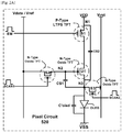
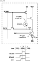
- FIG. 2A illustrates one suitable pixel circuit that can be used in the embodiments of the present disclosure.
- the first switching transistor (S1) includes a gate electrode connected to an emission signal line (EM).
- the first switching transistor (S1) has a source electrode connected to the first node (N1) and a drain electrode connected to a source electrode of a driving transistor (DT).
- One end of the first node (N1) is connected to a power voltage signal line (VDD).
- the driving transistor (DT) has a gate electrode connected to a second node (N2) and a drain electrode connected to a third node (N3).
- the pixel circuit also includes a second switching transistor (S2), which has a source electrode connected to the data line (VDATA) to receive the data signal and a drain electrode connected to the second node (N2).
- the gate electrode of the second switching transistor (S2) is connected to the scan line (SCAN1) to turn on/off the second switching transistor (S2) according to the scan signal from the driving circuit at the periphery of the active area.
- a third switching transistor having a gate electrode connected to a second scan signal line (SCAN2).
- the third switching transistor (S3) has a source electrode connected to a third node (N3) and a drain electrode to an initial signal line (VINI).
- the anode of the OLED is connected to the third node (N3) and the cathode of the OLED is connected to the second power voltage line (VSS).
- the first capacitor (CS1) includes one end connected to the second node (N2) and the other end connected to the third node (N3).
- the second capacitor (CS2) includes one end connected to the first node (N1) and another end connected to the third node (N3).
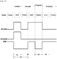
- FIG. 2B illustrates a timing diagram of an exemplary 4T2C pixel circuit shown in FIG. 2A .
- the timing of the TFTs in the pixel circuit depicted in FIG. 2B is based on the operation of the pixel circuit implemented with N-TYPE oxide TFTs.
- each of the TFTs in the pixel circuit serves a different function during the operation. As such, operating conditions and requirements of the TFTs can vary even among the TFTs forming the pixel circuit.
- the reference voltage and the data voltage are alternately applied on the data line during driving of the pixel.
- Applying the scan signal on the Scan1 and the EM signal for 1H makes it convenient to maintain the initial and sampling timing.
- a permanent shift in the V th may occur from the stress caused by continuous flow of current for extended period of time, which is called positive bias stress.
- Such a problem is more prevalent in oxide TFTs than the LTPS TFTs.
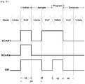
- the TFT serving as the emission transistor is in "On" state for much longer than other TFTs. With the current flowing over almost the entire frame, the emission transistor formed of oxide TFT may cause various undesired problems in the display.
- the emission transistor of the pixel circuit is formed of a P-TYPE LTPS TFT while N-TYPE oxide TFTs are used for the rest of the pixel circuit.
- the exemplary 4T2C pixel circuit may operate as the timing diagram shown in FIG. 2C . Under this operating scheme, problems associated with PBTS in the emission transistor of the pixel circuit can be suppressed.
- Similar configuration can be used for any other TFTs of the pixel circuit and/or the driving circuit on the backplane. That is, other TFTs in the pixel circuit, which are subjected to more PBTS compared to other TFTs of the pixel circuit may be formed of a P-TYPE LTPS TFT. Accordingly, certain transistors of a pixel circuit configured to receive current for longer period of time can be formed with P-Type LTPS TFTs, which may be stronger against the positive bias stress.
- the TFTs that are connected to a storage capacitor or to a node connected to a storage capacitor may be formed of the oxide TFT to minimize leakage therefrom.
- the LTPS TFT can be strategically placed within the circuit to remove bias remaining in a node between oxide TFTs during their off state and minimize the bias stress (e.g., PBTS, NBTS).
- oxide TFT and the LTPS TFT combination in the pixel circuit described in reference to FIGS. 2A - 2C are merely illustrative. As such, the use of oxide TFT and LTPS TFT combination within a pixel circuit may be applied in various pixel circuit designs other than the 4T2C pixel circuit designs shown above.
- FIG. 3A illustrates an exemplary 5T1C pixel circuit implemented with N-Type oxide TFTs and the timing diagram describing the operation of the pixel circuit.
- FIG. 3B illustrates the same 5T1C pixel circuit, but implemented with a combination of N-Type oxide TFTs and P-Type LTPS TFTs, and the timing diagram describing the operation of the pixel circuit.
- the switching transistors having their gate electrode connected to the second scan line (Scan2) and the emission signal line (EM) are configured to receive current for longer period of time during the operation.
- those switching transistors are likely to be affected by the positive bias stress, which may lead to non-uniformity in the display. Accordingly, those transistors in the pixel circuit operating under the higher stress condition (e.g., turned on for a longer period of time) can be formed with P-Type LTPS TFT instead of the N-Type LTPS TFT, which may be affected less by the positive bias stress.
- the transistor controlled by the second scan line (Scan2) and the emission signal line (EM) can be formed of a P-Type LTPS TFT.
- the operation of the pixel circuit may change as shown in the timing diagram of FIG. 3B .
- Employing a combination of P-Type LTPS TFTs and N-Type oxide TFTs in the pixel circuit may eliminate a need for providing an invert circuit in the driving circuit of the backplane. Elimination of the invert circuit from the driving circuit means elimination of clock signals associated in controlling the invert circuit. The power consumption of the display can be reduced with a reduced number of clock signals. Also, a typical invert circuit is implemented with several TFTs (e.g., 5-8), which may add up to a considerable number of TFTs in the entire driving circuit. Accordingly, eliminating the invert circuit along with the associated clock signal lines from the backplane can save a considerable space from the non-display area of the display, which allows to for a narrower bezel in the display.
- CMOS circuit or an inverter circuit in the backplane, it can be implemented with a combination of an LTPS TFT and an oxide TFT.
- a P-type LTPS TFT and an N-Type oxide TFT can be used to implement a CMOS circuit in the driving circuit and/or the pixel circuit.
- the invert circuit can be simplified by using a combination of N-Type oxide TFT and P-Type LTPS TFT.
- the number of TFTs required to implement an invert circuit can be significantly reduced (e.g., 2) when it is implemented with a combination of N-Type oxide TFT and P-Type LTPS TFT.
- the array of pixel circuits may be implemented with oxide TFTs, while the driving circuits implemented on the backplane may be implemented with a combination of N-Type LTPS TFTs and P-Type LTPS TFTs.
- N-Type LTPS TFTs and P-Type LTPS TFTs can be used to implement a CMOS circuit (e.g., CMOS invert circuit) in the GIP, whereas oxide TFTs are employed in at least some part of the pixel circuits.
- the gate out signal from the GIP with a CMOS circuit can be controlled by DC signals or logic high/low signals. This allows for more stable control of the gate line during the blank period to suppress current leakage from the pixel circuit to the GIP or to suppress unintended activation of the pixels connected the gate line.
- pixel circuits can be implemented with a combination of oxide TFTs and LTPS TFTs to reduce the number of gate lines.
- a pixel circuit may be supplied with a number of signal lines for controlling the TFTs in a pixel circuit.
- the first signal line may be configured to supply a high level signal (VGH) to the pixel circuit when a second signal line supplies a low level signal (VGL).
- VGH high level signal
- one or more TFTs controlled by the first signal line may be formed of one of an N-Type oxide TFT and a P-Type LTPS TFT
- one or more TFTs controlled by the second signal line may be formed of another one of an N-Type oxide TFT and a P-Type LTPS TFT.
- a single signal line can be provided to those TFTs, which were controlled by the first and the second signal lines.
- any pair of TFTs in a pixel circuit which are configured to receive signals of the opposite level from each other, may be formed of a combination of an N-Type oxide TFT and a P-Type LTPS TFT.
- a first TFT in a pixel circuit may be configured to receive a high level signal (VGH) while a low level signal (VGL) is supplied to a second TFT in the same pixel circuit.
- one of the TFTs can be formed of an N-Type oxide TFT while the other TFT can be formed of a P-Type LTPS TFT, and the gates of these two TFTs can be connected to the same signal line.
- the high level signal (VGH) on the signal line activates one TFT while the low level signal (VGL) activates another TFT of the pixel circuit.
- FIG. 4 illustrates an exemplary pixel circuit provided with a combination of N-Type oxide TFTs and P-Type LTPS TFTs, which are configured to share a gate signal line.
- the pixel circuit shown in FIG. 4 includes six transistors (denoted M1 through M6) and a storage capacitor (Cst).
- M1 through M6 two different signal lines (i.e., VG1, VG2) are used to control the TFTs of the pixel circuit.
- the first TFT (M1) is a driving TFT in the pixel circuit.
- the first TFT (M1) has an electrode connected to the driving voltage line (VDD) and another electrode connected to a node (NET2).
- the second transistor (M2) has an electrode connected to the anode of the OLED element and another electrode connected to the node (NET2) between the first TFT (M1).
- the third transistor (M3) has an electrode connected to a reference voltage line (Vref) and configured to supply the reference voltage to the node (NET1), which is connected to the gate of the driving TFT (M1).
- the fourth TFT (M4) has an electrode connected to the reference voltage line (Vref) and another electrode connected to the node (NET3), which is connected to the storage capacitor (C1).
- the fifth TFT (M5) has an electrode connected to the node (NET2) between the driving TFT (M1) and the emission TFT (M2).
- the sixth transistor (M6) has an electrode connected to the data signal line of the display, and transmit the data signal from the data signal line in response to the signal from the gate line.
- the gate of a third TFT is connected to the first signal line (VG1) and the gates of the second TFT (M2), the fourth TFT (M4), the fifth TFT (M5) and the sixth TFT (M6) are connected to the second signal line (VG2).
- the second TFT (M2) and the fourth TFT (M4) are configured to be activated in the opposite timing from the fifth TFT (M5) and the sixth TFT (M6).
- the second TFT (M2) and the fourth TFT (M4) can be formed of the N-Type oxide TFT, and the fifth TFT (M5) and the sixth TFT (M6) can be formed of the P-Type LTPS TFT.
- the second TFT (M2) and the fourth TFT (M4) can be formed of P-Type LTPS TFT, and the fifth TFT (M5) and the sixth TFT (M6) can be formed of N-Type oxide TFT.
- the second TFT (M2) and the fourth TFT (M4) need to be activated at the opposite timing from that of the fifth TFT (M5) and the sixth TFT (M6)
- the second TFT (M2) and the fourth TFT (M4) can be formed of P-Type oxide TFT while the fifth TFT (M5) and the sixth TFT (M6) are formed of N-Type LTPS TFT.
- the second TFT (M2) and the fourth TFT (M4) can be formed of N-Type LTPS TFT while the fifth TFT (M5) and the sixth TFT (M6) are formed of P-Type oxide TFT.
- TFTs in one stage of a shift register of a GIP may be formed of an oxide TFT while one of the TFTs in another stage of the shift register is formed of an LTPS TFT.
- one of the TFTs in a pixel circuit may be formed of an oxide TFT while one of the TFTs in another pixel circuit may be formed of an LTPS TFT.
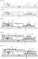
- FIG. 5 illustrates an exemplary configuration of two pixel circuits, in which one of the pixel circuit is provided with an N-Type oxide TFT and the other pixel circuit is provided with a P-Type LTPS TFT.
- the first pixel circuit include a switching TFT formed of N-Type oxide TFT, and the corresponding TFT in the second pixel circuit is formed of a P-Type LTPS TFT.
- the first pixel circuit may be associated with a pixel of an odd line of the display, whereas the second pixel circuit may be associated with a pixel of an even line of the display.
- the gate of the N-Type oxide TFT of the first pixel circuit and the gate of the P-Type LTPS TFT of the second pixel circuit may be connected to a single gate line. In this way, the number of gate lines can be reduced in the display.
- the TFTs in each of the pixel circuit that shares the gate line may be the TFT configured to provide the data signal in response to the gate signal on the shared gate line.
- signals for controlling the pixel circuit may be set as follow: a data signal (VDATA) between 0 and 5V, a VGL of -10V, a VGO of 3V, a VGH of 15V, a VREF of IV.
- VDATA data signal
- the threshold voltage of the N-Type oxide TFT in the first pixel circuit and the P-Type LTPS TFT in the second pixel circuit may be set to 3V and -2.5V, respectively.
- the driving TFT connected to the OLED element in the first and second pixel circuits are not particularly limited, and they can be formed with any one of N-Type oxide TFT and P-Type LTPS TFT. If desired, the driving TFTs in the first pixel circuit and the second pixel circuit may be formed of different type of TFT from each other.
- the N-Type oxide TFT in the first pixel circuit and the P-Type LTPS TFT in the second pixel circuit are not limited to the TFT connected to the data signal line.
- other switching TFTs for instance a TFT connected to a reference signal line in the two pixel circuits, may be configured with different kinds of TFT from each other.
- the use of N-Type oxide TFT and P-Type LTPS TFT in the adjacent pixel circuits allows to reduce the number of gate line at the border of the two adjacent pixels, which may be particularly advantageous in a transparent display.
- the emissive region of the two adjacent pixels e.g., an odd line pixel and an even line pixel
- This configuration would make the transparent regions of the pixel to be positioned next to each other, which may improve the transparency of the display.
- Providing multiple types of TFTs on the same substrate as described in the present disclosure can be a challenging process.
- Some of the processes related in forming one type of TFT may damage or otherwise degrade the other type of TFT on the same backplane.
- annealing process for forming poly-crystalized semiconductor layer may damage the metal oxide semiconductor layer.
- fabricating a backplane with multiple types of TFTs may increase the number of masks, which in turn, lowers the yield and increases the manufacturing cost of the display.
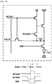
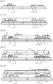
- FIG. 6A is a cross-sectional view of an exemplary backplane implemented with multiple types of TFTs, according to an embodiment of the present disclosure.
- the metal oxide semiconductor layer can be patterned and selectively turned into electrodes of the LTPS TFT. More specifically, the layer of metal oxide semiconductor can be patterned as the active layer of the oxide TFT as well as one or more electrodes for the LTPS TFT. Post treatments, such as plasma treatment for increasing the carrier concentration or other implantation and/or thermal annealing processes, can be performed on some part of the patterned oxide semiconductor layer to turn the treated parts to serve as S/D regions between a channel region of the oxide TFT. The same process can be performed on the metal oxide layer patterned in place of one or more electrodes of the LTPS TFT so that it can serve as the electrode of the LTPS TFT.
- Post treatments such as plasma treatment for increasing the carrier concentration or other implantation and/or thermal annealing processes
- the metal oxide layer for forming the active layer of the oxide TFT as one or more electrodes in the LTPS TFT allows to reduce the number of masks needed in fabricating the backplane with multiple types of TFTs. Also, some of the insulation layers used in forming the LTPS TFT on the backplane can also serve as the insulation layer for the oxide TFT, albeit the specific function of the insulation layer may differ in the TFT. Utilizing an insulation layer of one type of TFT for an insulation layer of another type of TFT can also help in reducing the number of masks and simplifying the manufacturing process of the backplane.
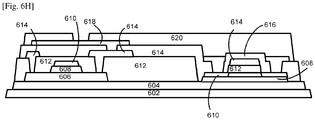
- FIG. 6B-6H are cross-sectional views showing the configuration of the oxide TFT and the LTPS TFT during fabricating them on the backplane in the configuration depicted in FIG. 6A .
- a buffer layer 604 is formed on the substrate 602.
- a poly-silicon active layer 606 is formed on the buffer layer 604.
- Fabricating the poly-silicon active layer 606 of the LTPS TFT as shown in FIG. 6B would require a first mask (for poly-silicon active layer patterning).
- the laser annealing or other suitable processes for turning the amorphous silicon layer into the poly-silicon active layer 606 can be performed prior to the deposition of the metal oxide layer on the backplane.
- a first insulation layer 608 is provided on the poly-silicon active layer 606 to serve as a gate insulation layer (GI_L).
- the first insulation layer 608 is provided in the area for forming the oxide TFT (denoted as the "oxide TFT region") to serve as an extra buffer layer under the active layer of the oxide TFT.
- a metal oxide layer 610 is provided in the oxide TFT region, which would serve as the active layer of the oxide TFT.
- the metal oxide layer 610 is patterned on the gate insulation layer 608 in the LTPS TFT region. In other words, the metal oxide layer 610 is used as a gate electrode of the LTPS TFT and also as an active layer of the oxide TFT.
- one or more post-processes can be performed to increase the conductivity at selective parts of the metal oxide layer 610.
- the post-process can be performed to increase the conductivity at the S/D regions of the metal oxide layer 610 at the oxide TFT region.
- the post-process which forms the S/D regions in the metal oxide layer 610 of the oxide TFT, also increases the conductivity of the metal oxide layer 610 patterned on the gate insulation layer 608 at the LTPS TFT region. With the increased conductivity, the metal oxide layer 610 at the LTPS TFT region can effectively serve as a gate electrode of the LTPS TFT. It should be appreciated that the use of the metal oxide layer 610 to form the gate electrode of the LTPS TFT reduces a mask required in fabricating the backplane with the multiple types of TFTs.
- a layer of photo-resist can be provided over the metal oxide layer in the LTPS TFT region and the oxide TFT region, then selective parts of the PR layer is exposed through a second mask.
- a half-tone mask (HTM) process can be used so that the PR layer over the channel region of the oxide TFT region is left with a higher thickness than the PR layer over other parts of the metal oxide layer 610. That is, the PR layer over the channel region in the active layer of the oxide TFT can be left with a greater thickness than the PR layer over the S/D regions in the active layer of the oxide TFT.
- the PR layer over the channel region in the active layer of the oxide TFT can be left with a greater thickness than the PR layer over the metal oxide layer 610 in the LTPS TFT region, which is to serve as the gate electrode of the LTPS TFT.
- the extra thickness of the PR layer over the channel region of the oxide TFT allows to maintain the semiconductor property even after the processes for increasing the conductivity of the metal oxide layer 610 at the LTPS TFT region to turn it into the gate electrode.
- a second insulation layer 612 is provided over the LTPS TFT region and the oxide TFT region.
- a third mask can be used to pattern the second insulation layer 612 so that it serves as the interlayer dielectric layer (ILD) at the LTPS TFT region and also as the gate insulation layer (GI_O) in the oxide TFT region.
- a half-tone mask process can be used to control the thicknesses of the second insulation layer 612 at the selective regions. More specifically, the second insulation layer 612 can be formed in a first thickness, which is suitable to serve as the ILD in the LTPS TFT region.
- the second insulation layer 612 can be formed in a second thickness, which is suitable to serve as the gate insulation layer (GI_O) in the oxide TFT region.
- the thickness of the second insulation layer 612 may have a thickness of about 4000 ⁇ in the LTPS TFT region and may have a thickness of about 2000 ⁇ in the oxide TFT region.
- contact holes can be provided with contact holes, which expose the S/D regions of the poly-silicon active layer 606.
- a first metal layer 614 is provided over the second insulation layer 612.
- a fourth mask is used to pattern the first metal layer 614.
- the first metal layer 614 is patterned to form the S/D electrodes of the LTPS TFT.
- the first metal layer 614 is patterned to form a gate electrode of the oxide TFT.
- a third insulation layer 616 is provided over the LTPS TFT region and the oxide TFT region.
- the third insulation layer 616 is patterned to serve as the passivation layer over the S/D electrodes of the LTPS TFT and to serve as the ILD for the oxide TFT. Since the third insulation 616 serves as the passivation layer over the S/D electrodes of the LTPS TFT, one or more contact holes through the third insulation layer 616 can be provided to expose some parts of the S/D electrodes of the LTPS TFT. The contact holes through the third insulation layer 616 can be used to connect a signal line and/or other electrodes to the S/D of the LTPS TFT.
- the second metal layer 618 is provided over the third insulation layer 616.
- the second metal layer 618 can be patterned as a inter metal layer (INT) at the LTPS TFT region, which is connected to the S/D electrode of the LTPS TFT through the contact hole in the third insulation layer 616.
- INT inter metal layer
- the second metal layer 618 in the LTPS TFT region is described as the inter-metal layer in this particular embodiment, the functionality of the second metal layer 618 is not limited as such. Accordingly, the second metal layer 618 may serves as a signal line, an electrode and various other purposes in the backplane.
- the second metal layer 618 can be patterned to serve as the S/D electrodes of the oxide TFT.
- a fourth insulation layer 620 is provided over both the LTPS TFT and the oxide TFT.
- the fourth insulation layer 620 may be a planarization layer (PLN) for providing a planar surface over the LTPS TFT region and the oxide TFT region.
- PPN planarization layer
- a contact hole may be provided through the fourth insulation layer 620 to expose a selective parts of the second metal layer 618.
- the inter-metal layer (INT) is exposed through a contact hole of the fourth insulation layer 620.
- the fourth insulation layer 620 serves as the planarization layer (PLN) over both the LTPS TFT and the oxide TFT, it also serves as a passivation layer over the S/D electrodes of the oxide TFT. Accordingly, in some embodiments, the fourth insulation layer 620 may be provided with one or more contact holes for exposing the S/D electrodes of the oxide TFT.
- PPN planarization layer
- a third metal layer 622 can be patterned in the desired region over the fourth insulation layer 620 by using a eighth mask.
- the third metal layer 622 can be in contact with the second metal layer 618 through the fourth insulation layer 620.
- the third metal layer 622 may be in contact with the inter-metal layer (INT) as shown in FIG. 6A .
- the third metal layer 622 patterned over the fourth insulation layer 620 can be in contact with the S/D electrode of the oxide TFT.
- the LTPS TFT and the oxide TFT shown in FIG. 6A can be configured to serve various purposes in the backplane. Any combined use of the oxide TFT and the LTPS TFT described in the present disclosure may be achieved with the configuration of the oxide TFT and the LTPS TFT shown in FIG. 6A .
- the LTPS TFT shown in FIG. 6A may be a TFT included in a driving circuit, while the oxide TFT may be a TFT included in a pixel circuit.
- the LTPS TFT shown in FIG. 6A may be a TFT included in a pixel circuit, while the oxide TFT may be a TFT included in a driving circuit.
- Both of the LTPS TFT and the oxide TFT shown in FIG. 6A may the TFTs included in single pixel circuit or in multiple pixel circuits. Also, both of the LTPS TFT and the oxide TFT shown in FIG. 6A may the TFTs included in single pixel circuit or in multiple pixel circuits.
- the functionality of the third metal layer 622 in the backplane may vary depending on the location of the third metal layer 622 within the backplane as well as the location and the function of the TFT connected to the third metal layer 622.
- the LTPS TFT shown in FIG. 6A may be a driving TFT in a pixel circuit, and the third metal layer 622 may serve as an anode of an OLED element.
- the LTPS TFT shown in FIG. 6A may be a switching TFT in a pixel circuit, and the third metal layer 622 may be a signal line transmitting a signal from a driving circuit.
- the LTPS TFT may be one of the TFTs implementing a driving circuit provided in the non-display area of the display, and the third metal layer 622 may serve as a signal line for transmitting a signal from the respective driving circuit.
- the third metal layer 622 may be in contact with the S/D electrodes of the oxide TFT, and provides a function associated with the respective oxide TFT.
- the gate of the LTPS TFT is formed with the layer of metal oxide, which forms the semiconductor layer of the oxide TFT.
- several insulation layers provided in the backplane serve as one purpose in the LTPS TFT region and another purpose in the oxide TFT region. This can provide more efficient way of manufacturing the backplane with multiple types of TFTs.
- FIG. 7A illustrates another exemplary configuration of an oxide TFT and an LTPS TFT of a backplane, according to an embodiment of the present disclosure.
- FIG. 7B-7G are cross-sectional views showing the configuration of the oxide TFT and the LTPS TFT during fabricating them on the backplane in the configuration depicted in FIG. 7A .
- the configuration of the buffer layer 704 and the poly-silicon active layer 706 on the substrate 702 is the same as the configuration described in reference with FIG. 6B . Accordingly, forming the gate electrode of the LTPS TFT with the metal oxide layer 710 requires two masks.
- the interlayer dielectric layers (ILD) for the LTPS TFT and the oxide TFT were formed by different insulation layers in the configuration of FIG. 6A . That is, the interlayer dielectric layers (ILD) for the LTPS TFT was formed with the second insulation layer 612 whereas the interlayer dielectric layers (ILD) for the oxide TFT was formed with the third insulation layer 616.
- the same insulation layer is used to serve as the interlayer dielectric layer (ILD) for both the LTPS TFT and the oxide TFT.
- the second insulation layer 712 that serves the interlayer dielectric layers (ILD) for the LTPS TFT also serves as the interlayer dielectric layers (ILD) for the oxide TFT.
- the second insulation layer 712 serves yet another purpose for the oxide TFT.
- the second insulation layer 712 is patterned with a third mask, so that it also serves as the gate insulation (GI_O) of the oxide TFT.
- GI_O gate insulation
- ILD interlayer dielectric layers
- ILD interlayer dielectric layer
- a thickness of the interlayer dielectric layer (ILD) suitable for the LTPS TFT may be different from the thickness of the interlayer dielectric layer (ILD) suitable for the oxide TFT.
- the thickness of the gate insulation layer (GI_O) generally differs from the thickness of the interlayer dielectric layer (ILD).
- the second insulation layer 712 can be patterned using a half-tone mask (HTM) to control its thickness at different parts of the backplane.
- HTM half-tone mask
- the second insulation layer 712 in the LTPS TFT region, the second insulation layer 712 may be provided in a first thickness that is suitable to serve as the interlayer dielectric layer (ILD) for the LTPS TFT.
- parts of the second insulation 712 serving as the interlayer dielectric layer (ILD) can be provided in a second thickness while other parts serving as the gate insulation layer (GI_O) is provided in a third thickness.
- the first thickness and the second thickness for the second insulation layer 712 in the LTPS TFT region and the oxide TFT region may be the same.
- the second insulation layer 712 may be provided in a thickness of about 4000 ⁇ where it serves as the interlayer dielectric layer (ILD), but provided in a thickness of about 2000 ⁇ where it serves as the gate insulation (GI_O) of the oxide TFT.
- the first metal layer 714 is provided over the second insulation layer 712. With a fourth mask, the first metal layer 714 is patterned to provide S/D electrodes of the LTPS TFT as well as the gate electrode of the oxide TFT. Unlike the configuration of shown in FIG. 6A , the first metal layer 714 also forms the S/D electrodes of the oxide TFT as shown in FIG. 7E . In other words, all of the electrodes for the LTPS TFT and the oxide TFT, excluding the gate electrode of the LTPS TFT, are formed with the same metal layer (i.e., the first metal layer 714). At least one less mask is needed by forming the S/D electrodes of the oxide TFT and the LTPS TFT along with the gate electrode of the oxide TFT with a single metal layer.
- the third insulation layer 716 and the fourth insulation layer 720 is provided over the first metal layer 714.
- the third insulation layer 716 may serve as the passivation layer for the S/D electrodes of both the LTPS TFT and the oxide TFT.
- the fourth insulation layer 720 is provided over the third insulation layer 716.
- the fourth insulation layer 720 can serve as the planarization layer that provides a planar surface over the LTPS TFT and the oxide TFT.
- the third insulation 616 serves as a passivation layer for the LTPS TFT needs to serve as the interlayer dielectric layer (ILD) for the oxide TFT. Therefore, contact holes for S/D electrodes must be created before providing the fourth insulation layer 620 over the third insulation layer 616, then a separate process is required to create another contact hole(s) through the fourth insulation layer 620.
- ILD interlayer dielectric layer
- each of the third insulation layer 716 and the fourth insulation layer 720 serves the same function for the LTPS TFT and the oxide TFT.
- the third insulation layer 716 serves as the passivation layer for both the LTPS TFT and the oxide TFT, and therefore there is no need for patterning the third insulation layer 716 prior to providing the fourth insulation layer 720.
- contact hole(s) for S/D electrode contact can be created with a single mask after providing the third insulation layer 716 and the fourth insulation layer 720.
- a second metal layer 718 is provided over the fourth insulation layer 716 to be in contact with the S/D electrode of one of the TFTs.
- the second metal layer 718 is shown as being in contact with the S/D electrode of the oxide TFT through a contact hole provided in the third and fourth insulation layers.
- a contact hole may be provided in the third and fourth insulation layers so that the second metal layer 718 can be in contact with the S/D electrode of the LTPS TFT.
- the LTPS TFT and the oxide TFT may be used within the backplane for any of the exemplary configurations described in the present disclosure. Therefore, the functionality of the second metal layer 718 can vary depending on the use of the particular TFT which it is in contact with.
- FIG. 8 is a plane view of an exemplary a pixel circuit configured with multiple types of TFTs (i.e., at least one LTPS TFT and at least one oxide TFT).
- the gate line and the S/D line may cross each other.
- the gate line and the S/D line should not be in contact with each other.
- the metal oxide layer which is used as the active layer oxide TFT, can also be used as a means for routing the lines across each other without creating a short.
- the first line 810 is arranged in a horizontal direction and the second line 820 is arranged in a vertical direction.
- the first line 810 is provided in multiple pieces (e.g., 810A, 810B) that are separated at the area denoted "X". Otherwise, the first line 810 would run across the second line 820, creating a short between the lines at the crossing area "X.”
- the metal oxide layer under the metal layer of the first and second lines (810, 820) is patterned so that it is provided at the crossing area "X.” Conductivity of the metal oxide layer in the crossing area "X" can be increased in the similar way as the metal oxide layer configured as the gate electrode of the LTPS TFT.
- Contact holes can be provided through the insulation layer provided over the metal oxide layer so that the first piece 810A and the second piece 810B of the first line 810 contact the metal oxide layer thereunder.
- the metal oxide layer provided at the crossing area "X" can serve as a bridge for connecting the pieces of the first line (810A, 810B). Accordingly, the first line 810 and the second line 820 can be routed across each other even in the embodiments where the S/D and the gate electrodes of a TFT are provided with a single metal layer.
- the metal oxide layer that serves as the active layer of the oxide TFT is described as composed of Indium-Gallium-Zinc-Oxide. However, this is merely illustrative. Various other compositions can be used for the metal oxide layer of the present disclosure.
- Examples of a constituent material of the metal oxide layer includes a quaternary metal oxide such as an indium-tin-gallium-zinc-oxide (In-Sn-Ga-Zn-O)-based material, a ternary metal oxide such as an indium-gallium-zinc-oxide (In-Ga-Zn-O)-based material, an indium-tin-zinc-oxide (In-Sn-Zn-O)-based material, an indium-aluminum-zinc-oxide (In-Al-Zn-O)-based material, an indium-hafnium-zinc-oxide (In-Hf-Zn-O)-based material, a tin-gallium-zinc-oxide (Sn-Ga-Zn-O)-based material, an aluminum-gallium-zinc-oxide (Al-Ga-Zn-O-based material) and a tin-aluminum-zinc-oxide (
Claims (12)
- Affichage (100), comportant :un substrat (602) défini avec une première zone et une seconde zone ;une couche de polysilicium à basse température (LTPS) (606) agencée dans la première zone ;une première couche d'isolation (608) agencée sur la couche LTPS (606) dans la première zone ;une couche d'oxyde de métal (610) agencée dans la première zone et la seconde zone, la couche d'oxyde de métal (610) dans la première zone étant agencée sur la première couche d'isolation (608) ;une deuxième couche d'isolation (612) agencée dans la première zone et la seconde zone, la deuxième couche d'isolation (612) dans la première zone ayant des trous de contact pour exposer au moins une certaine partie de la couche LTPS (606) sous celle-ci, et la deuxième couche d'isolation (612) dans la seconde zone est agencée sur la couche d'oxyde de métal (610) pour exposer au moins deux parties de la couche d'oxyde de métal (610) séparées par une partie recouverte par la deuxième couche d'isolation (612) ;une première couche métallique (614) dans la première zone et la seconde zone, la première couche métallique (614) dans la première zone étant en contact avec les parties exposées de la couche LTPS, et la première couche métallique (614) dans la seconde zone étant isolée de la couche d'oxyde de métal (616) par la deuxième couche d'isolation (612) sous celle-ci ;une troisième couche d'isolation (616) recouvrant la première couche métallique (614) dans la première zone et la seconde zone ;une deuxième couche métallique (618) agencée dans la première zone et la seconde zone, la deuxième couche métallique (618) dans la première zone étant en contact avec la première couche métallique (614) via un trou de contact à travers la troisième couche d'isolation (616), et la deuxième couche métallique (618) dans la seconde zone étant en contact avec la couche d'oxyde de métal (610) via un trou de contact à travers la troisième couche d'isolation (616) ; etune quatrième couche d'isolation (620) agencée dans la première zone et la seconde zone au-dessus de la deuxième couche métallique (618),dans lequel la couche d'oxyde de métal (610) dans la première zone a une conductivité électrique plus élevée que la partie de la couche d'oxyde de métal (610) recouverte par la deuxième couche d'isolation (612) dans la seconde zone,dans lequel la couche de polysilicium à basse température (LTPS) (606) sert de couche active d'un TFT LTPS et la couche d'oxyde de métal (610) dans la seconde zone sert de couche active d'un TFT à oxyde,dans lequel la couche d'oxyde de métal (610) dans la première zone sert d'électrode de grille du TFT LTPS,dans lequel la première couche métallique (614) fournit une électrode de source et une électrode de drain du TFT LTPS dans la première zone, et la première couche métallique (614) fournit une électrode de grille du TFT à oxyde dans la seconde zone, etdans lequel la deuxième couche métallique (618) fournit une électrode de source et une électrode de drain du TFT à oxyde dans la seconde zone.
- Affichage (100) selon la revendication 1, comportant en outre une troisième couche métallique (622) sur la quatrième couche d'isolation (620), la troisième couche métallique (622) étant en contact avec la deuxième couche métallique (618) dans la première zone ou la deuxième couche métallique dans la seconde zone via un trou de contact à travers la quatrième couche d'isolation (620).
- Affichage (100) selon la revendication 1, dans lequel la deuxième couche d'isolation (612) sert de couche diélectrique d'intercouche du TFT LTPS dans la première zone et sert de couche d'isolation de grille du TFT à oxyde dans la seconde zone.
- Affichage (100) selon la revendication 1, dans lequel la deuxième couche d'isolation (612) qui est intercalée entre la couche d'oxyde de métal (610) et la première couche métallique (614) dans la seconde zone est plus mince que la deuxième couche d'isolation (612) agencée dans la première zone.
- Affichage (100) selon la revendication 1, dans lequel la troisième couche d'isolation (616) sert de couche de passivation du TFT LTPS dans la première zone et sert de couche diélectrique d'intercouche pour le TFT à oxyde dans la seconde zone.
- Affichage (100) selon la revendication 1, dans lequel la troisième couche métallique (622) qui est en contact avec la deuxième couche métallique (618) est une anode d'un élément électroluminescent organique.
- Affichage (100) selon la revendication 1, dans lequel la troisième couche métallique (622) qui est en contact avec la deuxième couche métallique (618) est une ligne de signal.
- Affichage (100) selon la revendication 1, comportant : un réseau de transistors à couches minces (TFT) incluant le TFT à oxyde et le TFT LTPS.
- Affichage (100) selon la revendication 8, dans lequel au moins un TFT à oxyde est agencé dans une zone d'affichage et au moins un TFT LTPS est agencé dans une zone de non-affichage.
- Affichage (100) selon la revendication 9, comportant en outre : un circuit de pixel associé à un pixel d'affichage dans la zone d'affichage ; un circuit d'attaque dans la zone de non-affichage configuré pour fournir une pluralité de signaux au circuit de pixel, dans lequel le circuit de pixel est mis en œuvre avec le TFT à oxyde et le circuit d'attaque est mis en œuvre avec le TFT LTPS.
- Affichage (100) selon la revendication 8, dans lequel le réseau de TFT inclut un réseau de circuits de pixels associés à une pluralité de pixels d'affichage dans une zone d'affichage, dans lequel l'un des circuits de pixels associés à un seul pixel d'affichage inclut le TFT à oxyde et le TFT LTPS.
- Affichage (100) selon la revendication 8, comportant en outre un circuit d'attaque dans une zone de non-affichage configuré pour fournir une pluralité de signaux à un réseau de circuits de pixels associés à une pluralité de pixels d'affichage dans une zone d'affichage, dans lequel le circuit d'attaque dans la zone de non-affichage inclut ledit TFT à oxyde et ledit TFT LTPS.
Applications Claiming Priority (6)
| Application Number | Priority Date | Filing Date | Title |
|---|---|---|---|
| US201461944464P | 2014-02-25 | 2014-02-25 | |
| US201461944469P | 2014-02-25 | 2014-02-25 | |
| KR20140195119 | 2014-12-31 | ||
| US14/588,180 US9449994B2 (en) | 2014-02-25 | 2014-12-31 | Display backplane having multiple types of thin-film-transistors |
| KR20140195302 | 2014-12-31 | ||
| PCT/KR2015/013731 WO2016108473A1 (fr) | 2014-12-31 | 2015-12-15 | Fond de panier de dispositif d'affichage comportant de multiples types de transistors à couches minces |
Publications (3)
| Publication Number | Publication Date |
|---|---|
| EP3241240A1 EP3241240A1 (fr) | 2017-11-08 |
| EP3241240A4 EP3241240A4 (fr) | 2018-08-22 |
| EP3241240B1 true EP3241240B1 (fr) | 2020-11-18 |
Family
ID=53883010
Family Applications (2)
| Application Number | Title | Priority Date | Filing Date |
|---|---|---|---|
| EP15875558.7A Pending EP3241209A4 (fr) | 2014-02-25 | 2015-12-09 | Face arrière de dispositif d'affichage ayant de multiples types de transistors en couches minces |
| EP15875567.8A Active EP3241240B1 (fr) | 2014-02-25 | 2015-12-15 | Fond de panier de dispositif d'affichage comportant de multiples types de transistors à couches minces |
Family Applications Before (1)
| Application Number | Title | Priority Date | Filing Date |
|---|---|---|---|
| EP15875558.7A Pending EP3241209A4 (fr) | 2014-02-25 | 2015-12-09 | Face arrière de dispositif d'affichage ayant de multiples types de transistors en couches minces |
Country Status (3)
| Country | Link |
|---|---|
| US (3) | US9406705B2 (fr) |
| EP (2) | EP3241209A4 (fr) |
| CN (1) | CN107004682B (fr) |
Families Citing this family (69)
| Publication number | Priority date | Publication date | Assignee | Title |
|---|---|---|---|---|
| US9818765B2 (en) | 2013-08-26 | 2017-11-14 | Apple Inc. | Displays with silicon and semiconducting oxide thin-film transistors |
| KR102207916B1 (ko) | 2013-10-17 | 2021-01-27 | 삼성디스플레이 주식회사 | 박막트랜지스터 어레이 기판, 유기 발광 표시 장치 및 박막트랜지스터 어레이 기판의 제조 방법 |
| CN103715226A (zh) * | 2013-12-12 | 2014-04-09 | 京东方科技集团股份有限公司 | Oled阵列基板及其制备方法、显示面板及显示装置 |
| JP2015146543A (ja) * | 2014-02-04 | 2015-08-13 | 株式会社リコー | 画像処理装置、画像処理方法及び画像処理プログラム |
| US9276050B2 (en) * | 2014-02-25 | 2016-03-01 | Lg Display Co., Ltd. | Organic light emitting display device |
| CN103941507B (zh) * | 2014-04-02 | 2017-01-11 | 上海天马微电子有限公司 | 一种阵列基板、显示面板及显示装置 |
| US9543370B2 (en) * | 2014-09-24 | 2017-01-10 | Apple Inc. | Silicon and semiconducting oxide thin-film transistor displays |
| CN104867450B (zh) * | 2015-06-05 | 2017-09-19 | 京东方科技集团股份有限公司 | 阵列基板及其制作方法、显示装置 |
| US10332446B2 (en) * | 2015-12-03 | 2019-06-25 | Innolux Corporation | Driving circuit of active-matrix organic light-emitting diode with hybrid transistors |
| US11887537B2 (en) * | 2015-12-03 | 2024-01-30 | Innolux Corporation | Driving circuit of active-matrix organic light-emitting diode with hybrid transistors |
| US9818344B2 (en) * | 2015-12-04 | 2017-11-14 | Apple Inc. | Display with light-emitting diodes |
| JP2017224676A (ja) * | 2016-06-14 | 2017-12-21 | 株式会社ジャパンディスプレイ | 半導体装置及び表示装置 |
| US10297781B2 (en) * | 2016-06-30 | 2019-05-21 | Lg Display Co., Ltd. | Organic light emitting display device and driving method of the same |
| KR102561294B1 (ko) | 2016-07-01 | 2023-08-01 | 삼성디스플레이 주식회사 | 화소 및 스테이지 회로와 이를 가지는 유기전계발광 표시장치 |
| KR20180023155A (ko) | 2016-08-24 | 2018-03-07 | 삼성디스플레이 주식회사 | 유기발광 표시장치 |
| KR20180024817A (ko) * | 2016-08-31 | 2018-03-08 | 엘지디스플레이 주식회사 | 멀티 타입의 박막 트랜지스터를 포함하는 유기 발광 표시 장치 및 유기 발광 표시 장치 제조 방법 |
| US10043997B2 (en) | 2016-09-08 | 2018-08-07 | Apple Inc. | Encapsulation design for narrow border |
| US10482822B2 (en) | 2016-09-09 | 2019-11-19 | Apple Inc. | Displays with multiple scanning modes |
| US10109240B2 (en) | 2016-09-09 | 2018-10-23 | Apple Inc. | Displays with multiple scanning modes |
| US10424670B2 (en) * | 2016-12-30 | 2019-09-24 | Intel Corporation | Display panel with reduced power consumption |
| KR102636515B1 (ko) | 2017-01-06 | 2024-02-15 | 삼성디스플레이 주식회사 | 유기발광 표시장치 |
| CN107092900B (zh) * | 2017-06-01 | 2019-06-07 | 京东方科技集团股份有限公司 | 指纹识别电路及其驱动方法、显示面板 |
| US10566401B2 (en) * | 2017-06-28 | 2020-02-18 | Shenzhen China Star Optoelectronics Semiconductor Display Technology Co., Ltd. | Thin film transistor array substrate and preparing method therefor, and OLED display device |
| KR102369730B1 (ko) * | 2017-08-31 | 2022-03-02 | 엘지디스플레이 주식회사 | 유기 발광 표시 장치 |
| KR102480481B1 (ko) | 2017-09-22 | 2022-12-26 | 삼성디스플레이 주식회사 | 표시 장치 및 그 구동 방법 |
| CN107818991B (zh) * | 2017-10-23 | 2020-06-05 | 京东方科技集团股份有限公司 | 一种阵列基板及其制备方法、显示面板 |
| JP7171738B2 (ja) | 2018-01-11 | 2022-11-15 | アプライド マテリアルズ インコーポレイテッド | 金属酸化物スイッチを含み小型蓄電コンデンサを備えた薄膜トランジスタ |
| TWI653616B (zh) * | 2018-03-06 | 2019-03-11 | 友達光電股份有限公司 | 畫素電路 |
| US11137815B2 (en) | 2018-03-15 | 2021-10-05 | Nvidia Corporation | Metering GPU workload with real time feedback to maintain power consumption below a predetermined power budget |
| TWI670703B (zh) | 2018-06-15 | 2019-09-01 | 元太科技工業股份有限公司 | 畫素電路 |
| KR20190143309A (ko) | 2018-06-20 | 2019-12-30 | 삼성전자주식회사 | 픽셀 및 이를 포함하는 유기전계발광 표시장치 |
| KR102514242B1 (ko) | 2018-06-20 | 2023-03-28 | 삼성전자주식회사 | 픽셀 및 이를 포함하는 유기전계발광 표시장치 |
| CN110649003A (zh) * | 2018-06-26 | 2020-01-03 | 鸿富锦精密工业(深圳)有限公司 | 半导体基板、阵列基板、逆变器电路及开关电路 |
| JP2020017558A (ja) * | 2018-07-23 | 2020-01-30 | 株式会社ジャパンディスプレイ | 表示装置 |
| KR20200019308A (ko) | 2018-08-13 | 2020-02-24 | 삼성디스플레이 주식회사 | 유기 발광 표시 장치 |
| CN109256397B (zh) | 2018-09-20 | 2021-09-21 | 合肥鑫晟光电科技有限公司 | 显示基板及其制备方法、显示装置 |
| TWI699892B (zh) * | 2018-09-21 | 2020-07-21 | 友達光電股份有限公司 | 電子裝置及其製造方法 |
| CN109326633B (zh) * | 2018-09-30 | 2022-01-28 | 厦门天马微电子有限公司 | 一种显示面板及显示装置 |
| KR102614573B1 (ko) | 2018-10-22 | 2023-12-18 | 삼성디스플레이 주식회사 | 트랜지스터 기판 및 이를 포함하는 표시 장치 |
| AU2020100003B4 (en) * | 2019-01-28 | 2020-07-09 | Apple Inc. | Electronic devices having displays with compensation for oxide transistor threshold voltage |
| CN110379371B (zh) | 2019-01-28 | 2022-05-27 | 苹果公司 | 包括具有氧化物晶体管阈值电压补偿的显示器的电子设备 |
| CN109584799A (zh) | 2019-02-02 | 2019-04-05 | 京东方科技集团股份有限公司 | 一种像素驱动电路、像素电路、显示面板和显示装置 |
| CN109686314B (zh) * | 2019-03-01 | 2021-01-29 | 京东方科技集团股份有限公司 | 像素电路、显示基板和显示装置 |
| US11488529B2 (en) | 2019-05-16 | 2022-11-01 | Apple Inc. | Display compensation using current sensing across a diode without user detection |
| CN110289269A (zh) * | 2019-06-26 | 2019-09-27 | 上海天马微电子有限公司 | 一种阵列基板、显示面板和显示装置 |
| CN110299322B (zh) * | 2019-07-03 | 2022-03-08 | 京东方科技集团股份有限公司 | 一种显示基板及其制作方法、显示装置 |
| WO2021053707A1 (fr) * | 2019-09-17 | 2021-03-25 | シャープ株式会社 | Dispositif d'affichage et procédé de commande associé |
| CN110649044B (zh) | 2019-09-30 | 2022-02-25 | 厦门天马微电子有限公司 | 阵列基板及其制作方法、显示面板和显示装置 |
| EP3806151A1 (fr) * | 2019-10-08 | 2021-04-14 | Imec VZW | Architecture de transistor à couche mince pour affichages à haute résolution |
| CN110824797B (zh) * | 2019-11-12 | 2022-05-06 | 昆山国显光电有限公司 | 透明显示面板、显示面板及其显示装置 |
| KR102632710B1 (ko) * | 2019-12-10 | 2024-02-02 | 엘지디스플레이 주식회사 | 화소 구동 회로를 포함한 전계발광 표시장치 |
| KR20210129294A (ko) | 2020-04-17 | 2021-10-28 | 삼성디스플레이 주식회사 | 표시 장치 및 그 제조 방법 |
| US11411081B2 (en) * | 2020-04-22 | 2022-08-09 | Globalfoundries U.S. Inc. | Field effect transistor (FET) stack and methods to form same |
| KR20210132791A (ko) | 2020-04-27 | 2021-11-05 | 삼성디스플레이 주식회사 | 발광 제어 구동부 및 이를 포함하는 표시 장치 |
| CN111755462B (zh) * | 2020-06-23 | 2021-10-08 | 武汉华星光电半导体显示技术有限公司 | 阵列基板及其制造方法 |
| CN111627387B (zh) | 2020-06-24 | 2022-09-02 | 京东方科技集团股份有限公司 | 像素驱动电路及其驱动方法、显示面板及显示装置 |
| US11417689B2 (en) | 2020-07-16 | 2022-08-16 | Wuhan China Star Optoelectronics Semiconductor Display Technology Co., Ltd. | Display panel |
| CN111564458B (zh) * | 2020-07-16 | 2020-10-23 | 武汉华星光电半导体显示技术有限公司 | 显示面板 |
| CN112201160B (zh) * | 2020-10-10 | 2022-08-09 | Oppo广东移动通信有限公司 | 显示屏、显示控制方法、电子设备及存储介质 |
| CN112271185B (zh) * | 2020-10-28 | 2024-01-30 | 武汉华星光电技术有限公司 | 阵列基板及其制备方法 |
| KR20220076872A (ko) * | 2020-12-01 | 2022-06-08 | 엘지디스플레이 주식회사 | 유기 발광 표시 장치 |
| CN114938418A (zh) * | 2021-02-04 | 2022-08-23 | 佳能株式会社 | 具有视线检测功能的取景器单元、摄像设备和附接配件 |
| US20230351958A1 (en) * | 2021-02-10 | 2023-11-02 | Boe Technology Group Co., Ltd. | Array substrate, display panel comprising the array substrate, and display device |
| CN113053914B (zh) * | 2021-03-08 | 2023-05-02 | 武汉华星光电半导体显示技术有限公司 | 显示面板及显示装置 |
| CN113078174B (zh) * | 2021-04-13 | 2022-08-12 | 厦门天马微电子有限公司 | 阵列基板、显示面板及显示装置 |
| JP2023007804A (ja) * | 2021-07-02 | 2023-01-19 | キヤノン株式会社 | 発光装置、表示装置、光電変換装置、電子機器、照明装置、移動体、ウェアラブルデバイスおよび画像形成装置 |
| CN114188354B (zh) * | 2021-12-02 | 2023-11-28 | 深圳市华星光电半导体显示技术有限公司 | 阵列基板及其制备方法和显示面板 |
| US20230176377A1 (en) | 2021-12-06 | 2023-06-08 | Facebook Technologies, Llc | Directional illuminator and display apparatus with switchable diffuser |
| CN114241998B (zh) * | 2021-12-27 | 2023-06-30 | 昆山国显光电有限公司 | 像素电路、显示装置和显示装置的驱动方法 |
Family Cites Families (27)
| Publication number | Priority date | Publication date | Assignee | Title |
|---|---|---|---|---|
| TW517393B (en) | 2001-11-09 | 2003-01-11 | Prime View Int Co Ltd | TFT LCD structure with protrusion structure and its manufacturing method |
| TW588463B (en) * | 2003-04-04 | 2004-05-21 | Au Optronics Corp | A method for forming a low temperature polysilicon complementary metal oxide semiconductor thin film transistor |
| JP3772889B2 (ja) * | 2003-05-19 | 2006-05-10 | セイコーエプソン株式会社 | 電気光学装置およびその駆動装置 |
| US7915723B2 (en) * | 2004-01-29 | 2011-03-29 | Casio Computer Co., Ltd. | Transistor array, manufacturing method thereof and image processor |
| US20060118869A1 (en) * | 2004-12-03 | 2006-06-08 | Je-Hsiung Lan | Thin-film transistors and processes for forming the same |
| KR101214205B1 (ko) * | 2005-12-02 | 2012-12-21 | 재단법인서울대학교산학협력재단 | 표시 장치 및 그 구동 방법 |
| TWI303888B (en) | 2006-07-21 | 2008-12-01 | Au Optronics Corp | Ltps-lcd structure and method for manufacturing the same |
| TWI412125B (zh) | 2007-07-17 | 2013-10-11 | Creator Technology Bv | 電子元件及電子元件之製法 |
| TWI332266B (en) | 2007-08-31 | 2010-10-21 | Au Optronics Corp | Method for manufacturing a pixel structure of a liquid crystal display |
| US20090085039A1 (en) | 2007-09-28 | 2009-04-02 | Tpo Displays Corp. | Image display system and fabrication method thereof |
| JP5135073B2 (ja) | 2008-06-18 | 2013-01-30 | 出光興産株式会社 | 有機薄膜トランジスタ |
| KR101100999B1 (ko) * | 2009-01-13 | 2011-12-29 | 삼성모바일디스플레이주식회사 | 씨모스 박막트랜지스터 및 그 제조방법과 이를 구비한 유기전계발광 표시장치 |
| KR101073301B1 (ko) * | 2009-07-15 | 2011-10-12 | 삼성모바일디스플레이주식회사 | 유기 전계발광 표시장치 및 그 제조방법 |
| KR101065407B1 (ko) * | 2009-08-25 | 2011-09-16 | 삼성모바일디스플레이주식회사 | 유기 발광 표시 장치 및 그 제조 방법 |
| KR101333783B1 (ko) | 2009-11-10 | 2013-11-29 | 삼성디스플레이 주식회사 | 유기 발광 표시 장치 및 그 제조 방법 |
| KR101611908B1 (ko) | 2009-11-11 | 2016-04-12 | 엘지디스플레이 주식회사 | 박막 트랜지스터 어레이 기판 및 이의 제조 방법 |
| KR101577234B1 (ko) | 2009-12-11 | 2015-12-14 | 엘지디스플레이 주식회사 | 패턴 형성 방법 및 박막 트랜지스터 어레이 기판의 제조 방법 |
| KR101084189B1 (ko) | 2010-01-21 | 2011-11-17 | 삼성모바일디스플레이주식회사 | 유기 발광 표시 장치 |
| TWI423194B (zh) | 2010-09-21 | 2014-01-11 | Waltop Int Corp | 整合電磁式感應輸入之平面顯示裝置與薄膜電晶體陣列基板 |
| CN102645801B (zh) | 2011-04-07 | 2014-10-29 | 京东方科技集团股份有限公司 | 薄膜晶体管阵列基板、彩膜基板、制作方法和显示设备 |
| CA2845768A1 (fr) | 2011-06-24 | 2012-12-27 | Sharp Kabushiki Kaisha | Dispositif d'affichage et methode de fabrication de celui-ci |
| KR101493226B1 (ko) | 2011-12-26 | 2015-02-17 | 엘지디스플레이 주식회사 | 유기 발광 다이오드 표시 장치의 화소 구동 회로의 특성 파라미터 측정 방법 및 장치 |
| TWI459368B (zh) | 2012-09-14 | 2014-11-01 | Au Optronics Corp | 顯示裝置及其閘極信號產生方法 |
| CN102881571B (zh) | 2012-09-28 | 2014-11-26 | 京东方科技集团股份有限公司 | 有源层离子注入方法及薄膜晶体管有源层离子注入方法 |
| CN103000632B (zh) * | 2012-12-12 | 2015-08-05 | 京东方科技集团股份有限公司 | 一种cmos电路结构、其制备方法及显示装置 |
| KR102034254B1 (ko) | 2013-04-04 | 2019-10-21 | 삼성디스플레이 주식회사 | 박막 트랜지스터 어레이 기판, 이를 포함하는 유기 발광 표시 장치 및 유기 발광 표시 장치의 제조 방법 |
| CN103715196B (zh) * | 2013-12-27 | 2015-03-25 | 京东方科技集团股份有限公司 | 一种阵列基板及其制作方法、显示装置 |
-
2014
- 2014-12-31 US US14/588,193 patent/US9406705B2/en active Active
- 2014-12-31 US US14/588,205 patent/US9634038B2/en active Active
- 2014-12-31 US US14/588,180 patent/US9449994B2/en active Active
-
2015
- 2015-12-09 CN CN201580064041.XA patent/CN107004682B/zh active Active
- 2015-12-09 EP EP15875558.7A patent/EP3241209A4/fr active Pending
- 2015-12-15 EP EP15875567.8A patent/EP3241240B1/fr active Active
Non-Patent Citations (1)
| Title |
|---|
| None * |
Also Published As
| Publication number | Publication date |
|---|---|
| US20150243718A1 (en) | 2015-08-27 |
| CN107004682A (zh) | 2017-08-01 |
| US9634038B2 (en) | 2017-04-25 |
| US20150243720A1 (en) | 2015-08-27 |
| US9406705B2 (en) | 2016-08-02 |
| US9449994B2 (en) | 2016-09-20 |
| EP3241209A4 (fr) | 2017-12-13 |
| US20150243719A1 (en) | 2015-08-27 |
| EP3241240A1 (fr) | 2017-11-08 |
| EP3241209A1 (fr) | 2017-11-08 |
| EP3241240A4 (fr) | 2018-08-22 |
| CN107004682B (zh) | 2020-06-19 |
Similar Documents
| Publication | Publication Date | Title |
|---|---|---|
| EP3241240B1 (fr) | Fond de panier de dispositif d'affichage comportant de multiples types de transistors à couches minces | |
| KR102404159B1 (ko) | 다수의 타입들의 박막 트랜지스터들을 갖는 디스플레이 백플레인 | |
| KR101658716B1 (ko) | 표시 장치 | |
| TWI649739B (zh) | 像素驅動電路及其驅動方法和電晶體的版圖結構 | |
| KR102566477B1 (ko) | 다수의 타입들의 박막 트랜지스터들을 갖는 디스플레이 백플레인 | |
| KR20230025508A (ko) | 다수의 타입들의 박막 트랜지스터들을 갖는 디스플레이 백플레인 | |
| KR102402602B1 (ko) | 다수의 타입들의 박막 트랜지스터들을 갖는 디스플레이 백플레인 | |
| KR20140127441A (ko) | 박막 트랜지스터 및 유기 발광 표시 장치 | |
| EP3241241B1 (fr) | Fond de panier d'affichage comprenant de multiples types de transistors en couches minces | |
| KR102394409B1 (ko) | 유기발광다이오드 표시장치 | |
| KR102658874B1 (ko) | 다수의 타입들의 박막 트랜지스터들을 갖는 디스플레이 백플레인 | |
| KR20240054421A (ko) | 다수의 타입들의 박막 트랜지스터들을 갖는 디스플레이 백플레인 |
Legal Events
| Date | Code | Title | Description |
|---|---|---|---|
| STAA | Information on the status of an ep patent application or granted ep patent |
Free format text: STATUS: THE INTERNATIONAL PUBLICATION HAS BEEN MADE |
|
| PUAI | Public reference made under article 153(3) epc to a published international application that has entered the european phase |
Free format text: ORIGINAL CODE: 0009012 |
|
| STAA | Information on the status of an ep patent application or granted ep patent |
Free format text: STATUS: REQUEST FOR EXAMINATION WAS MADE |
|
| 17P | Request for examination filed |
Effective date: 20170628 |
|
| AK | Designated contracting states |
Kind code of ref document: A1 Designated state(s): AL AT BE BG CH CY CZ DE DK EE ES FI FR GB GR HR HU IE IS IT LI LT LU LV MC MK MT NL NO PL PT RO RS SE SI SK SM TR |
|
| AX | Request for extension of the european patent |
Extension state: BA ME |
|
| DAV | Request for validation of the european patent (deleted) | ||
| DAX | Request for extension of the european patent (deleted) | ||
| REG | Reference to a national code |
Ref country code: DE Ref legal event code: R079 Ref document number: 602015062339 Country of ref document: DE Free format text: PREVIOUS MAIN CLASS: H01L0029786000 Ipc: H01L0027120000 |
|
| A4 | Supplementary search report drawn up and despatched |
Effective date: 20180725 |
|
| RIC1 | Information provided on ipc code assigned before grant |
Ipc: H01L 27/12 20060101AFI20180719BHEP Ipc: G09G 3/3233 20160101ALI20180719BHEP |
|
| GRAP | Despatch of communication of intention to grant a patent |
Free format text: ORIGINAL CODE: EPIDOSNIGR1 |
|
| STAA | Information on the status of an ep patent application or granted ep patent |
Free format text: STATUS: GRANT OF PATENT IS INTENDED |
|
| INTG | Intention to grant announced |
Effective date: 20200610 |
|
| GRAS | Grant fee paid |
Free format text: ORIGINAL CODE: EPIDOSNIGR3 |
|
| GRAA | (expected) grant |
Free format text: ORIGINAL CODE: 0009210 |
|
| STAA | Information on the status of an ep patent application or granted ep patent |
Free format text: STATUS: THE PATENT HAS BEEN GRANTED |
|
| AK | Designated contracting states |
Kind code of ref document: B1 Designated state(s): AL AT BE BG CH CY CZ DE DK EE ES FI FR GB GR HR HU IE IS IT LI LT LU LV MC MK MT NL NO PL PT RO RS SE SI SK SM TR |
|
| REG | Reference to a national code |
Ref country code: GB Ref legal event code: FG4D |
|
| REG | Reference to a national code |
Ref country code: CH Ref legal event code: EP |
|
| REG | Reference to a national code |
Ref country code: IE Ref legal event code: FG4D |
|
| REG | Reference to a national code |
Ref country code: DE Ref legal event code: R096 Ref document number: 602015062339 Country of ref document: DE |
|
| REG | Reference to a national code |
Ref country code: AT Ref legal event code: REF Ref document number: 1336712 Country of ref document: AT Kind code of ref document: T Effective date: 20201215 |
|
| REG | Reference to a national code |
Ref country code: AT Ref legal event code: MK05 Ref document number: 1336712 Country of ref document: AT Kind code of ref document: T Effective date: 20201118 |
|
| REG | Reference to a national code |
Ref country code: NL Ref legal event code: MP Effective date: 20201118 |
|
| PG25 | Lapsed in a contracting state [announced via postgrant information from national office to epo] |
Ref country code: GR Free format text: LAPSE BECAUSE OF FAILURE TO SUBMIT A TRANSLATION OF THE DESCRIPTION OR TO PAY THE FEE WITHIN THE PRESCRIBED TIME-LIMIT Effective date: 20210219 Ref country code: NO Free format text: LAPSE BECAUSE OF FAILURE TO SUBMIT A TRANSLATION OF THE DESCRIPTION OR TO PAY THE FEE WITHIN THE PRESCRIBED TIME-LIMIT Effective date: 20210218 Ref country code: FI Free format text: LAPSE BECAUSE OF FAILURE TO SUBMIT A TRANSLATION OF THE DESCRIPTION OR TO PAY THE FEE WITHIN THE PRESCRIBED TIME-LIMIT Effective date: 20201118 Ref country code: RS Free format text: LAPSE BECAUSE OF FAILURE TO SUBMIT A TRANSLATION OF THE DESCRIPTION OR TO PAY THE FEE WITHIN THE PRESCRIBED TIME-LIMIT Effective date: 20201118 Ref country code: PT Free format text: LAPSE BECAUSE OF FAILURE TO SUBMIT A TRANSLATION OF THE DESCRIPTION OR TO PAY THE FEE WITHIN THE PRESCRIBED TIME-LIMIT Effective date: 20210318 |
|
| PG25 | Lapsed in a contracting state [announced via postgrant information from national office to epo] |
Ref country code: AT Free format text: LAPSE BECAUSE OF FAILURE TO SUBMIT A TRANSLATION OF THE DESCRIPTION OR TO PAY THE FEE WITHIN THE PRESCRIBED TIME-LIMIT Effective date: 20201118 Ref country code: BG Free format text: LAPSE BECAUSE OF FAILURE TO SUBMIT A TRANSLATION OF THE DESCRIPTION OR TO PAY THE FEE WITHIN THE PRESCRIBED TIME-LIMIT Effective date: 20210218 Ref country code: IS Free format text: LAPSE BECAUSE OF FAILURE TO SUBMIT A TRANSLATION OF THE DESCRIPTION OR TO PAY THE FEE WITHIN THE PRESCRIBED TIME-LIMIT Effective date: 20210318 Ref country code: PL Free format text: LAPSE BECAUSE OF FAILURE TO SUBMIT A TRANSLATION OF THE DESCRIPTION OR TO PAY THE FEE WITHIN THE PRESCRIBED TIME-LIMIT Effective date: 20201118 Ref country code: LV Free format text: LAPSE BECAUSE OF FAILURE TO SUBMIT A TRANSLATION OF THE DESCRIPTION OR TO PAY THE FEE WITHIN THE PRESCRIBED TIME-LIMIT Effective date: 20201118 Ref country code: SE Free format text: LAPSE BECAUSE OF FAILURE TO SUBMIT A TRANSLATION OF THE DESCRIPTION OR TO PAY THE FEE WITHIN THE PRESCRIBED TIME-LIMIT Effective date: 20201118 |
|
| REG | Reference to a national code |
Ref country code: LT Ref legal event code: MG9D |
|
| PG25 | Lapsed in a contracting state [announced via postgrant information from national office to epo] |
Ref country code: HR Free format text: LAPSE BECAUSE OF FAILURE TO SUBMIT A TRANSLATION OF THE DESCRIPTION OR TO PAY THE FEE WITHIN THE PRESCRIBED TIME-LIMIT Effective date: 20201118 |
|
| PG25 | Lapsed in a contracting state [announced via postgrant information from national office to epo] |
Ref country code: RO Free format text: LAPSE BECAUSE OF FAILURE TO SUBMIT A TRANSLATION OF THE DESCRIPTION OR TO PAY THE FEE WITHIN THE PRESCRIBED TIME-LIMIT Effective date: 20201118 Ref country code: SK Free format text: LAPSE BECAUSE OF FAILURE TO SUBMIT A TRANSLATION OF THE DESCRIPTION OR TO PAY THE FEE WITHIN THE PRESCRIBED TIME-LIMIT Effective date: 20201118 Ref country code: CZ Free format text: LAPSE BECAUSE OF FAILURE TO SUBMIT A TRANSLATION OF THE DESCRIPTION OR TO PAY THE FEE WITHIN THE PRESCRIBED TIME-LIMIT Effective date: 20201118 Ref country code: EE Free format text: LAPSE BECAUSE OF FAILURE TO SUBMIT A TRANSLATION OF THE DESCRIPTION OR TO PAY THE FEE WITHIN THE PRESCRIBED TIME-LIMIT Effective date: 20201118 Ref country code: LT Free format text: LAPSE BECAUSE OF FAILURE TO SUBMIT A TRANSLATION OF THE DESCRIPTION OR TO PAY THE FEE WITHIN THE PRESCRIBED TIME-LIMIT Effective date: 20201118 Ref country code: SM Free format text: LAPSE BECAUSE OF FAILURE TO SUBMIT A TRANSLATION OF THE DESCRIPTION OR TO PAY THE FEE WITHIN THE PRESCRIBED TIME-LIMIT Effective date: 20201118 |
|
| REG | Reference to a national code |
Ref country code: CH Ref legal event code: PL |
|
| REG | Reference to a national code |
Ref country code: DE Ref legal event code: R097 Ref document number: 602015062339 Country of ref document: DE |
|
| PG25 | Lapsed in a contracting state [announced via postgrant information from national office to epo] |
Ref country code: MC Free format text: LAPSE BECAUSE OF FAILURE TO SUBMIT A TRANSLATION OF THE DESCRIPTION OR TO PAY THE FEE WITHIN THE PRESCRIBED TIME-LIMIT Effective date: 20201118 Ref country code: DK Free format text: LAPSE BECAUSE OF FAILURE TO SUBMIT A TRANSLATION OF THE DESCRIPTION OR TO PAY THE FEE WITHIN THE PRESCRIBED TIME-LIMIT Effective date: 20201118 |
|
| REG | Reference to a national code |
Ref country code: BE Ref legal event code: MM Effective date: 20201231 |
|
| PLBE | No opposition filed within time limit |
Free format text: ORIGINAL CODE: 0009261 |
|
| STAA | Information on the status of an ep patent application or granted ep patent |
Free format text: STATUS: NO OPPOSITION FILED WITHIN TIME LIMIT |
|
| 26N | No opposition filed |
Effective date: 20210819 |
|
| PG25 | Lapsed in a contracting state [announced via postgrant information from national office to epo] |
Ref country code: AL Free format text: LAPSE BECAUSE OF FAILURE TO SUBMIT A TRANSLATION OF THE DESCRIPTION OR TO PAY THE FEE WITHIN THE PRESCRIBED TIME-LIMIT Effective date: 20201118 Ref country code: IT Free format text: LAPSE BECAUSE OF FAILURE TO SUBMIT A TRANSLATION OF THE DESCRIPTION OR TO PAY THE FEE WITHIN THE PRESCRIBED TIME-LIMIT Effective date: 20201118 Ref country code: IE Free format text: LAPSE BECAUSE OF NON-PAYMENT OF DUE FEES Effective date: 20201215 Ref country code: LU Free format text: LAPSE BECAUSE OF NON-PAYMENT OF DUE FEES Effective date: 20201215 Ref country code: NL Free format text: LAPSE BECAUSE OF FAILURE TO SUBMIT A TRANSLATION OF THE DESCRIPTION OR TO PAY THE FEE WITHIN THE PRESCRIBED TIME-LIMIT Effective date: 20201118 |
|
| PG25 | Lapsed in a contracting state [announced via postgrant information from national office to epo] |
Ref country code: LI Free format text: LAPSE BECAUSE OF NON-PAYMENT OF DUE FEES Effective date: 20201231 Ref country code: SI Free format text: LAPSE BECAUSE OF FAILURE TO SUBMIT A TRANSLATION OF THE DESCRIPTION OR TO PAY THE FEE WITHIN THE PRESCRIBED TIME-LIMIT Effective date: 20201118 Ref country code: CH Free format text: LAPSE BECAUSE OF NON-PAYMENT OF DUE FEES Effective date: 20201231 |
|
| PG25 | Lapsed in a contracting state [announced via postgrant information from national office to epo] |
Ref country code: ES Free format text: LAPSE BECAUSE OF FAILURE TO SUBMIT A TRANSLATION OF THE DESCRIPTION OR TO PAY THE FEE WITHIN THE PRESCRIBED TIME-LIMIT Effective date: 20201118 |
|
| PG25 | Lapsed in a contracting state [announced via postgrant information from national office to epo] |
Ref country code: IS Free format text: LAPSE BECAUSE OF FAILURE TO SUBMIT A TRANSLATION OF THE DESCRIPTION OR TO PAY THE FEE WITHIN THE PRESCRIBED TIME-LIMIT Effective date: 20210318 Ref country code: TR Free format text: LAPSE BECAUSE OF FAILURE TO SUBMIT A TRANSLATION OF THE DESCRIPTION OR TO PAY THE FEE WITHIN THE PRESCRIBED TIME-LIMIT Effective date: 20201118 Ref country code: MT Free format text: LAPSE BECAUSE OF FAILURE TO SUBMIT A TRANSLATION OF THE DESCRIPTION OR TO PAY THE FEE WITHIN THE PRESCRIBED TIME-LIMIT Effective date: 20201118 Ref country code: CY Free format text: LAPSE BECAUSE OF FAILURE TO SUBMIT A TRANSLATION OF THE DESCRIPTION OR TO PAY THE FEE WITHIN THE PRESCRIBED TIME-LIMIT Effective date: 20201118 |
|
| PG25 | Lapsed in a contracting state [announced via postgrant information from national office to epo] |
Ref country code: MK Free format text: LAPSE BECAUSE OF FAILURE TO SUBMIT A TRANSLATION OF THE DESCRIPTION OR TO PAY THE FEE WITHIN THE PRESCRIBED TIME-LIMIT Effective date: 20201118 |
|
| PG25 | Lapsed in a contracting state [announced via postgrant information from national office to epo] |
Ref country code: BE Free format text: LAPSE BECAUSE OF NON-PAYMENT OF DUE FEES Effective date: 20201231 |
|
| PGFP | Annual fee paid to national office [announced via postgrant information from national office to epo] |
Ref country code: GB Payment date: 20231023 Year of fee payment: 9 |
|
| REG | Reference to a national code |
Ref country code: DE Ref legal event code: R082 Ref document number: 602015062339 Country of ref document: DE Representative=s name: TER MEER STEINMEISTER & PARTNER PATENTANWAELTE, DE |
|
| PGFP | Annual fee paid to national office [announced via postgrant information from national office to epo] |
Ref country code: FR Payment date: 20231024 Year of fee payment: 9 Ref country code: DE Payment date: 20231023 Year of fee payment: 9 |