EP3220416B1 - Method of forming bump sites on bond-pads - Google Patents
Method of forming bump sites on bond-pads Download PDFInfo
- Publication number
- EP3220416B1 EP3220416B1 EP17163986.7A EP17163986A EP3220416B1 EP 3220416 B1 EP3220416 B1 EP 3220416B1 EP 17163986 A EP17163986 A EP 17163986A EP 3220416 B1 EP3220416 B1 EP 3220416B1
- Authority
- EP
- European Patent Office
- Prior art keywords
- bond
- layer
- pads
- dielectric
- metal layer
- Prior art date
- Legal status (The legal status is an assumption and is not a legal conclusion. Google has not performed a legal analysis and makes no representation as to the accuracy of the status listed.)
- Expired - Lifetime
Links
Images

Classifications
-
- H—ELECTRICITY
- H10—SEMICONDUCTOR DEVICES; ELECTRIC SOLID-STATE DEVICES NOT OTHERWISE PROVIDED FOR
- H10W—GENERIC PACKAGES, INTERCONNECTIONS, CONNECTORS OR OTHER CONSTRUCTIONAL DETAILS OF DEVICES COVERED BY CLASS H10
- H10W20/00—Interconnections in chips, wafers or substrates
- H10W20/40—Interconnections external to wafers or substrates, e.g. back-end-of-line [BEOL] metallisations or vias connecting to gate electrodes
-
- H—ELECTRICITY
- H10—SEMICONDUCTOR DEVICES; ELECTRIC SOLID-STATE DEVICES NOT OTHERWISE PROVIDED FOR
- H10W—GENERIC PACKAGES, INTERCONNECTIONS, CONNECTORS OR OTHER CONSTRUCTIONAL DETAILS OF DEVICES COVERED BY CLASS H10
- H10W72/00—Interconnections or connectors in packages
- H10W72/01—Manufacture or treatment
- H10W72/012—Manufacture or treatment of bump connectors, dummy bumps or thermal bumps
-
- H—ELECTRICITY
- H10—SEMICONDUCTOR DEVICES; ELECTRIC SOLID-STATE DEVICES NOT OTHERWISE PROVIDED FOR
- H10W—GENERIC PACKAGES, INTERCONNECTIONS, CONNECTORS OR OTHER CONSTRUCTIONAL DETAILS OF DEVICES COVERED BY CLASS H10
- H10W72/00—Interconnections or connectors in packages
- H10W72/01—Manufacture or treatment
- H10W72/019—Manufacture or treatment of bond pads
-
- H—ELECTRICITY
- H10—SEMICONDUCTOR DEVICES; ELECTRIC SOLID-STATE DEVICES NOT OTHERWISE PROVIDED FOR
- H10W—GENERIC PACKAGES, INTERCONNECTIONS, CONNECTORS OR OTHER CONSTRUCTIONAL DETAILS OF DEVICES COVERED BY CLASS H10
- H10W72/00—Interconnections or connectors in packages
- H10W72/20—Bump connectors, e.g. solder bumps or copper pillars; Dummy bumps; Thermal bumps
- H10W72/251—Materials
- H10W72/252—Materials comprising solid metals or solid metalloids, e.g. PbSn, Ag or Cu
-
- H—ELECTRICITY
- H10—SEMICONDUCTOR DEVICES; ELECTRIC SOLID-STATE DEVICES NOT OTHERWISE PROVIDED FOR
- H10W—GENERIC PACKAGES, INTERCONNECTIONS, CONNECTORS OR OTHER CONSTRUCTIONAL DETAILS OF DEVICES COVERED BY CLASS H10
- H10W72/00—Interconnections or connectors in packages
- H10W72/20—Bump connectors, e.g. solder bumps or copper pillars; Dummy bumps; Thermal bumps
- H10W72/29—Bond pads specially adapted therefor
-
- H—ELECTRICITY
- H10—SEMICONDUCTOR DEVICES; ELECTRIC SOLID-STATE DEVICES NOT OTHERWISE PROVIDED FOR
- H10W—GENERIC PACKAGES, INTERCONNECTIONS, CONNECTORS OR OTHER CONSTRUCTIONAL DETAILS OF DEVICES COVERED BY CLASS H10
- H10W72/00—Interconnections or connectors in packages
- H10W72/90—Bond pads, in general
- H10W72/921—Structures or relative sizes of bond pads
- H10W72/923—Bond pads having multiple stacked layers
-
- H—ELECTRICITY
- H10—SEMICONDUCTOR DEVICES; ELECTRIC SOLID-STATE DEVICES NOT OTHERWISE PROVIDED FOR
- H10W—GENERIC PACKAGES, INTERCONNECTIONS, CONNECTORS OR OTHER CONSTRUCTIONAL DETAILS OF DEVICES COVERED BY CLASS H10
- H10W72/00—Interconnections or connectors in packages
- H10W72/90—Bond pads, in general
- H10W72/931—Shapes of bond pads
- H10W72/934—Cross-sectional shape, i.e. in side view
-
- H—ELECTRICITY
- H10—SEMICONDUCTOR DEVICES; ELECTRIC SOLID-STATE DEVICES NOT OTHERWISE PROVIDED FOR
- H10W—GENERIC PACKAGES, INTERCONNECTIONS, CONNECTORS OR OTHER CONSTRUCTIONAL DETAILS OF DEVICES COVERED BY CLASS H10
- H10W72/00—Interconnections or connectors in packages
- H10W72/90—Bond pads, in general
- H10W72/941—Dispositions of bond pads
- H10W72/9415—Dispositions of bond pads relative to the surface, e.g. recessed, protruding
-
- H—ELECTRICITY
- H10—SEMICONDUCTOR DEVICES; ELECTRIC SOLID-STATE DEVICES NOT OTHERWISE PROVIDED FOR
- H10W—GENERIC PACKAGES, INTERCONNECTIONS, CONNECTORS OR OTHER CONSTRUCTIONAL DETAILS OF DEVICES COVERED BY CLASS H10
- H10W72/00—Interconnections or connectors in packages
- H10W72/90—Bond pads, in general
- H10W72/951—Materials of bond pads
- H10W72/952—Materials of bond pads comprising metals or metalloids, e.g. PbSn, Ag or Cu
Definitions
- the present invention relates to interconnect structures with bond-pads, such as copper bond-pads, and methods of forming bump sites on bond-pads.
- Semiconductor devices and other types of microelectronic devices have a die attached to a ceramic chip carrier, organic printed circuit board, lead frame, or other type of interposing structure.
- the microelectronic dies can be attached to interposing structures using Direct Chip Attach (DCA), flip-chip bonding, or wire-bonding to electrically connect the integrated circuitry in the dies to the wiring of the interposing structures.
- DCA Direct Chip Attach
- flip-chip bonding flip-chip bonding
- wire-bonding to electrically connect the integrated circuitry in the dies to the wiring of the interposing structures.
- DCA or flip-chip methods very small bumps or balls of a conductive material (e.g., solder) are deposited onto the contacts of a die. The bumps are then connected to corresponding terminals on an interposing structure.
- Copper is widely used for the wiring in semiconductor devices.
- the wiring in the integrated circuitry of many high performance devices is composed of copper.
- the bond-pads of many microelectronic dies are also made from copper.
- One problem of copper bond-pads is that copper easily oxidizes and corrodes in the presence of oxygen and water. As a result, copper bond-pads must be protected to prevent oxidation and/or corrosion that could possibly impair or destroy the device.
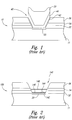
- Figure 1 is a cross-sectional view illustrating a portion of a microelectronic die 10 having substrate 11 with a copper bond-pad 20.
- the die 10 in Figure 1 further includes passivation layers including a first dielectric layer 32 (e.g., silicon dioxide), a second dielectric layer 34 (e.g., silicon nitride), and a third dielectric layer 36 (e.g., polyimide).
- the die 10 further includes a cap 40 having a barrier layer 42 and a metal layer 44 over the barrier layer 42.
- the cap 40 is formed by constructing a first mask over the first and second dielectric layers 32 and 34, and etching holes through the first and second dielectric layers 32 and 34 over the bond-pad 20.
- the barrier layer 42 and the metal layer 44 are then deposited onto the workpiece 10.
- the process of forming the cap 40 further includes constructing a second mask on top of the metal layer 44 from a resist 50, developing the resist 50 to expose the areas of the metal layer 44 over the upper portions of the third dielectric layer 36, and then etching the metal layer 44 and the barrier layer 42 down to the third dielectric layer 36 using a reactive ion etch.
- the resist 50 is subsequently stripped from the workpiece 10 to leave the cap 40 over the copper bond-pad 20.
- One problem with the copper interconnect structure illustrated in Figure 1 is that it is relatively expensive to manufacture because this process requires a first mask to form the openings over the bond-pad 20 and a second mask to form the pattern of resist 50 over the metal layer 44.
- Masks are expensive to construct because they require very expensive photolithography equipment to achieve the required tolerances in semiconductor devices.
- This process is also expensive because it uses a costly reactive ion etch to remove portions of the metal layer 44 and the barrier layer 42. This process is even further expensive because the resist 50 pools over the bond-pad 20 and is time consuming to remove.
- FIG. 2 is a cross-sectional view illustrating a portion of another embodiment of a microelectronic die 100 having a cap to protect a copper bond-pad.
- the die 100 illustrated in Figure 2 is similar to the die 10 illustrated in Figure 1 , and thus like reference numbers refer to like components in both of these figures.
- the die 100 illustrated in Figure 2 includes a cap 140 plated onto the bond-pad 20.
- the cap 140 is fabricated by constructing the first mask and forming a hole through the first and second dielectric layers 32 and 34 over the bond-pad 20. After forming the hole .over the bond-pad 20, the cap 140 is plated onto the bond-pad 20 using a series of different plating cycles.
- a palladium layer 142 can be plated directly onto the bond-pad 20 using a plating process.
- the palladium layer 142 provides a seed layer or nucleation layer for plating a nickel layer 144 onto the palladium layer 142 using another plating process.
- a silver layer 146 can be plated onto the palladium layer 142 before depositing the nickel layer 144, and/or a gold layer 148 can be deposited onto the nickel layer 144.
- cap 140 illustrated in Figure 2 One problem with the cap 140 illustrated in Figure 2 is that the nickel initially plates onto one of the underlying metal layers and then continues to plate upon itself. The nickel, however, does not bond to the sidewalls of the opening through the dielectric layers such that oxygen and moisture can migrate along the interface between the nickel and the dielectric layers 32, 34 and 36. Therefore, the contact 140 does not sufficiently protect the copper bond-pad 20 from oxidation and corrosion.
- US6451681 discloses a transitional metallurgy structure covering an exposed portion of a bond pad. After forming the transitional metallurgy structure, a passivation layer is formed overlying the transitional metallurgy structure. The passivation layer is then lithographically patterned and etched to form an opening that exposes portions of the transitional metallurgy structure. An optional polyimide (die coat) layer is then formed over the passivation layer. The polyimide layer is lithographically patterned and then etched (or developed) to form a die coat opening that exposes the opening defined in the passivation layer and the exposed portions of the transitional metallurgy structure.
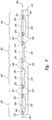
- Figure 3 is a cross-sectional view illustrating a portion of a microelectronic workpiece 300 including a plurality of protective caps on bond-pads to provide contact sites for solder balls, wire-bonds, metallization of redistribution layers, or other externally exposed conductive connectors.
- the microelectronic workpiece 300 includes a substrate 310 having a plurality of dies 320 formed in and/or on the substrate 310.
- the dies 320 include integrated circuitry 330 and bond-pads 340 electrically coupled to the integrated circuitry 330.
- the bond-pads 340 are typically copper pads, but the bond-pads 340 can be silver pads, gold pads, or other suitably conductive pads.
- the workpiece 300 further includes a dielectric structure 350 having a plurality of openings 352 arranged in a pattern over the bond-pads 340.
- the openings 352, more specifically, are configured to expose at least a portion of individual bond-pads 340 that are to be coupled to an external device.
- the workpiece further includes a plurality of caps 360 that cover the bond-pads 340 and are attached to sidewalls of the openings 352.
- the caps 360 are self-aligned with corresponding bond-pads 340 such that a separate mask is not used to electrically isolate the caps 360 in the openings 352.
- the caps 360 are expected to (a) be much less expensive to fabricate, and (b) provide better protection against oxygen and moisture.
- Figures 4A-4D are cross-sectional views illustrating the workpiece 300 at sequential stages of a process for fabricating one embodiment of the caps 360 shown in Figure 3 .
- Like reference numbers refer to like components in Figures 3-4D .
- Figure 4A illustrates an early stage of this process in which the dielectric structure 350 has been deposited onto the substrate 310, but the bond-pad 340 has not yet been exposed through the dielectric structure 350.
- the dielectric structure 350 includes a first dielectric layer 410, a second dielectric layer 412 on the first dielectric layer 410, and a third dielectric layer 414 on the second dielectric layer 412.
- the first dielectric layer 410 can be silicon dioxide and the second dielectric layer 412 can be silicon nitride.
- the first and second dielectric layers 410 and 412 can have a combined thickness of approximately 0.5 ⁇ m to 4 ⁇ m, and these layers typically have a total thickness of approximately 1 ⁇ m to 1.5 ⁇ m.
- the third dielectric layer 414 can be a polymer or other suitable dielectric material for forming a permanent mask on the second dielectric layer 412.
- the third dielectric layer 414 for example, can be a photo-active material deposited to a thickness of approximately 2-10 microns.
- One specific embodiment of the third dielectric layer 414 is a 4 micron thick layer of polybenzoxazole (PBO).
- PBO polybenzoxazole
- the third dielectric layer 414 is configured to inhibit dishing over the bond-pad 340 in a subsequent planarization procedure.
- the third dielectric layer 414 is sufficiently thick to protect the bond-pad 340 and any metal layers over the bond-pad 340 from excessive erosion during a subsequent chemical-mechanical planarization stage.
- the workpiece 300 can further include a diffusion barrier 415 between the copper bond-pad 340 and the dielectric structure 350 to prevent copper from diffusing into the dielectric structure 350.
- the diffusion barrier 415 is a 300 ⁇ thick layer of silicon carbide.
- the dielectric layers 410, 412, 414 and 415 can all be deposited using suitable chemical vapor deposition, sputtering, or other known processes for depositing these materials.
- Figure 4B illustrates a subsequent stage of the method in which an opening 352 has been formed through the dielectric structure 350 to expose a portion of the bond-pad 340.
- the opening 352 has a sidewall 420 and a shoulder 422 along the sidewall 420.
- the shoulder 422 can be a lateral notch or rim extending transversely with respect to the sidewall 420.
- the opening 352, for example, generally has a cross-sectional dimension parallel to the top surface of the bond-pad 340 of approximately 20 ⁇ m to 120 ⁇ m, and more generally 40 ⁇ m to 100 ⁇ m.
- the third dielectric layer 414 is composed of PBO and the opening 352 is formed by exposing and developing the PBO to create a mask having a hole aligned with the bond-pad 340.
- the portions of the second dielectric layer 412, first dielectric layer 410 and the diffusion barrier 415 over the bond-pad 340 are then etched to expose the upper surface of the bond-pad 340.
- the workpiece 300 is cleaned using a light plasma clean-up. The plasma clean-up also erodes the third dielectric layer 414 to further form the shoulder 422 at the interface between the second dielectric layer 412 and the third dielectric layer 414.
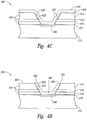
- Figure 4C illustrates the workpiece 300 at a subsequent stage after which conductive materials for the cap have been deposited onto the workpiece.
- the workpiece 300 includes a first conductive layer 430 deposited onto the dielectric structure 350 and the bond-pad 340, and a second conductive layer 440 deposited onto the first conductive layer 430.
- the first conductive layer 430 can be an optional intermediate layer that provides (a) a barrier to prevent migration or diffusion of materials between the bond-pad 340 and the second conductive layer 440, and/ or (b) adheres well to dielectric structure 350 and the bond-pads 340.
- the first conductive layer 430 is typically a barrier/adhesion layer having a thickness of approximately 300 ⁇ to 500 ⁇
- the second conductive layer 440 is typically a metal layer having a thickness of approximately 5,000 ⁇ to 30,000 ⁇ .
- the first conductive layer 430 can be composed of Ta, TaN, TiN, WN x , or other suitable materials that prevent copper from diffusing into the dielectric structure 350 and/or the second conductive layer 440.
- the second conductive layer 440 can be an aluminum layer having a thickness of approximately 8,000 ⁇ to 20,000 ⁇ .
- the second conductive layer 440 can alternatively be nickel or another suitable metal.
- the first conductive layer 430 in not needed because copper does not diffuse into nickel.
- the first and second conductive layers 430 and 440 conform to the sidewall 420 and the shoulder 422.
- the first and second conductive layers 430 and 440 have a step 442 seated with the shoulder 422.
- the interface between the step 442 and the shoulder 422 provides a strong barrier to block oxygen and moisture from reaching the bond-pad 340.
- the first and second conductive layers 430 and 440 also have a combined thickness less than that of the dielectric structure 350 such that these conductive layers do not completely fill the opening 352 in the dielectric structure 350.
- the combined thickness of the first and second conductive layers 430 and 440 is approximately 1 ⁇ m to 3 ⁇ m such that a significant void without conductive material exists in the opening 352 immediately after depositing the conductive layers.
- Figure 4D illustrates the workpiece 300 after a cap 460 has been formed over the bond-pad 340.
- the cap 460 is an embodiment of one of the caps 360 shown in Figure 3 .
- the cap 460 is formed by planarizing the workpiece 300 to remove the upper portions of the first and second conductive layers 430 and 440 from the top surface of the third dielectric layer 414.
- the workpiece 300 can be planarized by placing the workpiece 300 against a planarizing medium (not shown), and moving the workpiece and/or the planarizing medium relative to each other.
- the planarization process removes the upper portions of the first and second conductive layers 430 and 440 from the top surface of the third dielectric layer 414 without excessively eroding the portion of the first and second conductive layers 430 and 440 over the bond-pad 340.
- the third dielectric layer 414 protects the portion of the first and second conductive layers 430 and 440 over the bond-pad 340 because the relatively large thickness of the third dielectric layer 414 prevents the polishing pad from projecting into the opening to the extent that it causes unacceptable "dishing" in the second conductive layer 440. Although no dishing is shown in the portion of the second conductive layer 440 over the bond-pad 340, some dishing may be acceptable.
- the third dielectric layer 414 has a planarized upper surface 450 and the cap 460 has a planarized portion 462 that is an extension of the planarized upper surface 450.
- the planarizing process electrically isolates the cap 460 on the bond-pad 340 without having to form a second mask over the second conductive layer 440.
- the cap 460 therefore, is self-aligned with the bond-pad 340.
- cap 460 illustrated in Figure 4D is it is expected to be less expensive to produce than the cap 40 illustrated and described above with reference to Figure 1 .
- the cap 460 is manufactured using only a single mask to form the openings 352 through the dielectric structure 350.
- the caps 460 are self-aligned with the bond-pads 340 because the planarizing procedure described with reference to Figure 4D removes the upper portions of the first and second conductive layers 430 and 440 from the top surface of the dielectric structure 350 without using a second mask.
- the cap 40 illustrated in Figure 1 requires a first mask to form the opening through the dielectric layers and a second mask to pattern the resist 50.
- the cap 40 illustrated in Figure 1 requires an expensive reactive ion etch to remove the exposed portions of the conductive layers, and the resist 50 must be stripped from the cap 40.
- the single planarizing process used to form the cap 460 is much less expensive than forming a second mask on the workpiece, etching the metal layers using a reactive ion etch, and cleaning the resist. Therefore, the cap 460 illustrated in Figure 4D is expected to be cost effective to produce.
- the embodiment of the cap 460 illustrated in Figure 4D is further expected to provide exceptionally good protection of the copper bond-pad 40.
- the first conductive layer 430 bonds or otherwise adheres to the sidewall 420
- the second conductive layer 440 bonds to the first conductive layer 430.
- the length of the interface between the cap 460 and the dielectric structure 350 is relatively long. As a result, oxygen and moisture are less likely to reach the surface of the copper bond-pad 340.
- the interface between the shoulder 422 and the step 442 further inhibits air and moisture from reaching the copper bond-pad 340.
- the second conductive layer 440 typically has a higher coefficient of thermal expansion than the dielectric structure 350.
- the second conductive layer 440 when it cools after it has been deposited, it contracts inwardly and downwardly to a greater extent than the dielectric structure 350 contracts such that the step 442 presses downward against the shoulder 422.
- the second conductive layer 440 effectively forms a seal between the step 442 and the shoulder 422 to further inhibit oxygen, moisture or other contaminants from reaching the bond-pad 340.
- the dielectric structure enables the use of chemical-mechanical planarization to remove the upper portions of the first and second conductive layers 430 and 440 without a mask.
- chemical-mechanical planarization was not thought to be a viable option for removing the upper portions of the first and second conductive layers 430 and 440 because the polishing pad would project into the openings and cause dishing in the caps.
- the embodiment of the process illustrated in Figures 4A-4D enables the use of chemical-mechanical planarization by configuring the dielectric structure 350 to prevent or at least mitigate dishing of the second conductive layer 440 in the region over the bond-pad 340.
- one particular embodiment of the procedure illustrated in Figures 4A-4D forms the third dielectric layer 414 to a thickness of approximately 4 microns so that the planarizing pad does not "dish" into the second conductive layer 440 to an unacceptable extent before the upper portions of the first and second conductive layers 430 and 440 have been removed from the third dielectric layer 414.
- Figures 5A-5C illustrate a method for forming a cap defining an example of the present disclosure of one of the caps 360 illustrated in Figure 3 .
- Like reference numbers refer to like components in Figures 3-5C .
- Figure 5A illustrates an early stage of this embodiment in which the workpiece 300 has a dielectric structure 505 including a first dielectric layer 510 and a second dielectric layer 512.
- the first dielectric layer 510 can be silicon dioxide
- the second dielectric layer 512 can be silicon nitride.
- the workpiece 300 can further include a barrier layer 513 between the copper bond-pad 340 and the dielectric structure 505 to prevent copper from diffusing into the dielectric structure 505.
- the dielectric 505 further includes an opening 352 having a sidewall 520 projecting from the bond-pad 340.
- the first and second dielectric layers 510 and 512 can be deposited onto the substrate 310, and then the opening 352 can be etched through the first and second dielectric layers 510 and 512 using a mask. The mask is then stripped from the workpiece 300.
- Figure 5B illustrates the workpiece 300 at a subsequent stage of the method.
- the workpiece includes a first conductive layer 530 deposited onto the second dielectric layer 512 and the bond-pad 340.
- the workpiece further includes a second conductive layer 540 deposited onto the first conductive layer 530, and a sacrificial material 550 deposited onto the second conductive layer 540.
- the first conductive layer 530 can be a barrier layer
- the second conductive layer 540 can be aluminum or another suitable metal
- the sacrificial material 550 can be a resist.
- the structure and compositions of the first and second conductive layers 530 and 540 can be the same as the first and second conductive layers 430 and 440 described above with reference to Figures 4A-D .
- Figure 5C illustrates the workpiece 300 after the upper portions of the first and second conductive layers 530 and 540 have been removed using a planarization process to form a cap 560 over the bond-pad 340.
- the upper portions of the first and second conductive layers 530 and 540 are removed from the workpiece 300 by pressing the workpiece 300 against a planarizing medium, and moving the workpiece and/or the planarizing medium relative to each other in a chemical-mechanical planarization process.
- the second dielectric layer 512 has a planarized surface 515 and the cap 560 has a planarized portion 562.
- planarizing processes described above with reference to Figures 4D and 5C can be purely a mechanical process or a chemical-mechanical process.
- the bond-pads, conductive layers and dielectric layers moreover, can be composed of different materials and/or have different thicknesses than those described above.
- a redistribution structure can be fabricated on top of the dielectric structure and caps such that the metallization in the redistribution structures is electrically coupled to the caps over the bond-pads. Accordingly, the invention is not limited except as by the appended claims.
Landscapes
- Internal Circuitry In Semiconductor Integrated Circuit Devices (AREA)
Applications Claiming Priority (3)
| Application Number | Priority Date | Filing Date | Title |
|---|---|---|---|
| US11/032,975 US7282433B2 (en) | 2005-01-10 | 2005-01-10 | Interconnect structures with bond-pads and methods of forming bump sites on bond-pads |
| PCT/US2006/000881 WO2006074470A1 (en) | 2005-01-10 | 2006-01-10 | Interconnect structures with bond-pads and methods of forming bump sites on bond-pads |
| EP06718008.3A EP1842233B1 (en) | 2005-01-10 | 2006-01-10 | Method of forming bump sites on bond-pads |
Related Parent Applications (2)
| Application Number | Title | Priority Date | Filing Date |
|---|---|---|---|
| EP06718008.3A Division EP1842233B1 (en) | 2005-01-10 | 2006-01-10 | Method of forming bump sites on bond-pads |
| EP06718008.3A Division-Into EP1842233B1 (en) | 2005-01-10 | 2006-01-10 | Method of forming bump sites on bond-pads |
Publications (2)
| Publication Number | Publication Date |
|---|---|
| EP3220416A1 EP3220416A1 (en) | 2017-09-20 |
| EP3220416B1 true EP3220416B1 (en) | 2018-10-03 |
Family
ID=36282804
Family Applications (2)
| Application Number | Title | Priority Date | Filing Date |
|---|---|---|---|
| EP17163986.7A Expired - Lifetime EP3220416B1 (en) | 2005-01-10 | 2006-01-10 | Method of forming bump sites on bond-pads |
| EP06718008.3A Expired - Lifetime EP1842233B1 (en) | 2005-01-10 | 2006-01-10 | Method of forming bump sites on bond-pads |
Family Applications After (1)
| Application Number | Title | Priority Date | Filing Date |
|---|---|---|---|
| EP06718008.3A Expired - Lifetime EP1842233B1 (en) | 2005-01-10 | 2006-01-10 | Method of forming bump sites on bond-pads |
Country Status (6)
| Country | Link |
|---|---|
| US (3) | US7282433B2 (https=) |
| EP (2) | EP3220416B1 (https=) |
| JP (1) | JP5321873B2 (https=) |
| KR (1) | KR100918129B1 (https=) |
| TW (1) | TWI387018B (https=) |
| WO (1) | WO2006074470A1 (https=) |
Families Citing this family (45)
| Publication number | Priority date | Publication date | Assignee | Title |
|---|---|---|---|---|
| US7091124B2 (en) | 2003-11-13 | 2006-08-15 | Micron Technology, Inc. | Methods for forming vias in microelectronic devices, and methods for packaging microelectronic devices |
| US8084866B2 (en) | 2003-12-10 | 2011-12-27 | Micron Technology, Inc. | Microelectronic devices and methods for filling vias in microelectronic devices |
| US20050247894A1 (en) | 2004-05-05 | 2005-11-10 | Watkins Charles M | Systems and methods for forming apertures in microfeature workpieces |
| US7232754B2 (en) * | 2004-06-29 | 2007-06-19 | Micron Technology, Inc. | Microelectronic devices and methods for forming interconnects in microelectronic devices |
| US7425499B2 (en) | 2004-08-24 | 2008-09-16 | Micron Technology, Inc. | Methods for forming interconnects in vias and microelectronic workpieces including such interconnects |
| SG120200A1 (en) | 2004-08-27 | 2006-03-28 | Micron Technology Inc | Slanted vias for electrical circuits on circuit boards and other substrates |
| US7300857B2 (en) | 2004-09-02 | 2007-11-27 | Micron Technology, Inc. | Through-wafer interconnects for photoimager and memory wafers |
| US7271482B2 (en) | 2004-12-30 | 2007-09-18 | Micron Technology, Inc. | Methods for forming interconnects in microelectronic workpieces and microelectronic workpieces formed using such methods |
| US7282433B2 (en) | 2005-01-10 | 2007-10-16 | Micron Technology, Inc. | Interconnect structures with bond-pads and methods of forming bump sites on bond-pads |
| TW200638497A (en) * | 2005-04-19 | 2006-11-01 | Elan Microelectronics Corp | Bumping process and bump structure |
| US7795134B2 (en) | 2005-06-28 | 2010-09-14 | Micron Technology, Inc. | Conductive interconnect structures and formation methods using supercritical fluids |
| US20070045812A1 (en) * | 2005-08-31 | 2007-03-01 | Micron Technology, Inc. | Microfeature assemblies including interconnect structures and methods for forming such interconnect structures |
| US7863187B2 (en) | 2005-09-01 | 2011-01-04 | Micron Technology, Inc. | Microfeature workpieces and methods for forming interconnects in microfeature workpieces |
| US7622377B2 (en) | 2005-09-01 | 2009-11-24 | Micron Technology, Inc. | Microfeature workpiece substrates having through-substrate vias, and associated methods of formation |
| US7262134B2 (en) | 2005-09-01 | 2007-08-28 | Micron Technology, Inc. | Microfeature workpieces and methods for forming interconnects in microfeature workpieces |
| US7271086B2 (en) * | 2005-09-01 | 2007-09-18 | Micron Technology, Inc. | Microfeature workpieces and methods of forming a redistribution layer on microfeature workpieces |
| US20070145367A1 (en) * | 2005-12-27 | 2007-06-28 | Taiwan Semiconductor Manufacturing Company, Ltd. | Three-dimensional integrated circuit structure |
| KR100731081B1 (ko) * | 2005-12-30 | 2007-06-22 | 동부일렉트로닉스 주식회사 | 패시베이션 형성 방법 |
| US7749899B2 (en) | 2006-06-01 | 2010-07-06 | Micron Technology, Inc. | Microelectronic workpieces and methods and systems for forming interconnects in microelectronic workpieces |
| US7745319B2 (en) * | 2006-08-22 | 2010-06-29 | Micron Technology, Inc. | System and method for fabricating a fin field effect transistor |
| US7629249B2 (en) | 2006-08-28 | 2009-12-08 | Micron Technology, Inc. | Microfeature workpieces having conductive interconnect structures formed by chemically reactive processes, and associated systems and methods |
| US7902643B2 (en) | 2006-08-31 | 2011-03-08 | Micron Technology, Inc. | Microfeature workpieces having interconnects and conductive backplanes, and associated systems and methods |
| KR20090075883A (ko) * | 2006-10-31 | 2009-07-09 | 어드밴스드 마이크로 디바이시즈, 인코포레이티드 | 알루미늄 단자 금속층이 없는 금속화층 스택 |
| DE102006051491A1 (de) * | 2006-10-31 | 2008-05-15 | Advanced Micro Devices, Inc., Sunnyvale | Metallisierungsschichtstapel mit einer Aluminiumabschlussmetallschicht |
| US8981548B2 (en) | 2007-05-25 | 2015-03-17 | Stats Chippac Ltd. | Integrated circuit package system with relief |
| SG150410A1 (en) | 2007-08-31 | 2009-03-30 | Micron Technology Inc | Partitioned through-layer via and associated systems and methods |
| US7939949B2 (en) * | 2007-09-27 | 2011-05-10 | Micron Technology, Inc. | Semiconductor device with copper wirebond sites and methods of making same |
| US7884015B2 (en) | 2007-12-06 | 2011-02-08 | Micron Technology, Inc. | Methods for forming interconnects in microelectronic workpieces and microelectronic workpieces formed using such methods |
| US8084854B2 (en) | 2007-12-28 | 2011-12-27 | Micron Technology, Inc. | Pass-through 3D interconnect for microelectronic dies and associated systems and methods |
| KR101037832B1 (ko) * | 2008-05-09 | 2011-05-31 | 앰코 테크놀로지 코리아 주식회사 | 반도체 디바이스 및 그 제조 방법 |
| US8253230B2 (en) | 2008-05-15 | 2012-08-28 | Micron Technology, Inc. | Disabling electrical connections using pass-through 3D interconnects and associated systems and methods |
| WO2009146373A1 (en) * | 2008-05-28 | 2009-12-03 | Mvm Technoloiges, Inc. | Maskless process for solder bumps production |
| JP2010251687A (ja) * | 2009-03-26 | 2010-11-04 | Sanyo Electric Co Ltd | 半導体装置 |
| US8148257B1 (en) * | 2010-09-30 | 2012-04-03 | Infineon Technologies Ag | Semiconductor structure and method for making same |
| KR101210352B1 (ko) | 2011-02-15 | 2012-12-10 | 에스케이하이닉스 주식회사 | 반도체 패키지 및 그의 제조방법 |
| WO2013033034A2 (en) * | 2011-08-26 | 2013-03-07 | Lawrence Livermore National Security, Llc | Method for making high-density electrical interconnections using rivet bonds |
| US20130140671A1 (en) * | 2011-12-06 | 2013-06-06 | Win Semiconductors Corp. | Compound semiconductor integrated circuit with three-dimensionally formed components |
| TWI473226B (zh) * | 2012-01-09 | 2015-02-11 | 穩懋半導體股份有限公司 | 具有三維元件之化合物半導體積體電路 |
| CN103208472B (zh) * | 2012-01-12 | 2016-03-02 | 稳懋半导体股份有限公司 | 具有三维元件的复合物半导体集成电路 |
| US9609752B1 (en) | 2013-03-15 | 2017-03-28 | Lockheed Martin Corporation | Interconnect structure configured to control solder flow and method of manufacturing of same |
| US9487396B2 (en) * | 2014-09-04 | 2016-11-08 | Invensense, Inc. | Release chemical protection for integrated complementary metal-oxide-semiconductor (CMOS) and micro-electro-mechanical (MEMS) devices |
| US9627224B2 (en) * | 2015-03-30 | 2017-04-18 | Stmicroelectronics, Inc. | Semiconductor device with sloped sidewall and related methods |
| US11721784B2 (en) | 2017-03-30 | 2023-08-08 | Vuereal Inc. | High efficient micro devices |
| CN110709989B (zh) | 2017-03-30 | 2023-12-01 | 维耶尔公司 | 垂直固态装置 |
| KR20230139247A (ko) | 2022-03-25 | 2023-10-05 | 삼성전자주식회사 | 반도체 패키지 및 그 제조방법 |
Family Cites Families (37)
| Publication number | Priority date | Publication date | Assignee | Title |
|---|---|---|---|---|
| US5114826A (en) * | 1989-12-28 | 1992-05-19 | Ibm Corporation | Photosensitive polyimide compositions |
| US5773359A (en) * | 1995-12-26 | 1998-06-30 | Motorola, Inc. | Interconnect system and method of fabrication |
| US5749997A (en) * | 1995-12-27 | 1998-05-12 | Industrial Technology Research Institute | Composite bump tape automated bonding method and bonded structure |
| US5706977A (en) * | 1996-03-04 | 1998-01-13 | The Procter & Gamble Company | Modular display device |
| US5736456A (en) * | 1996-03-07 | 1998-04-07 | Micron Technology, Inc. | Method of forming conductive bumps on die for flip chip applications |
| US5702977A (en) * | 1997-03-03 | 1997-12-30 | Taiwan Semiconductor Manufacturing Company, Ltd. | Shallow trench isolation method employing self-aligned and planarized trench fill dielectric layer |
| US6441487B2 (en) * | 1997-10-20 | 2002-08-27 | Flip Chip Technologies, L.L.C. | Chip scale package using large ductile solder balls |
| US6251528B1 (en) | 1998-01-09 | 2001-06-26 | International Business Machines Corporation | Method to plate C4 to copper stud |
| US6107180A (en) * | 1998-01-30 | 2000-08-22 | Motorola, Inc. | Method for forming interconnect bumps on a semiconductor die |
| EP0949672A3 (en) | 1998-04-08 | 2002-09-11 | Texas Instruments Incorporated | PO Flow for copper metallization |
| US6268114B1 (en) * | 1998-09-18 | 2001-07-31 | Taiwan Semiconductor Manufacturing Company, Ltd | Method for forming fine-pitched solder bumps |
| DE19843624C1 (de) * | 1998-09-23 | 2000-06-15 | Siemens Ag | Integrierte Schaltungsanordnung und Verfahren zu deren Herstellung |
| US6130141A (en) * | 1998-10-14 | 2000-10-10 | Lucent Technologies Inc. | Flip chip metallization |
| US6500750B1 (en) * | 1999-04-05 | 2002-12-31 | Motorola, Inc. | Semiconductor device and method of formation |
| US6251775B1 (en) * | 1999-04-23 | 2001-06-26 | International Business Machines Corporation | Self-aligned copper silicide formation for improved adhesion/electromigration |
| US6133136A (en) | 1999-05-19 | 2000-10-17 | International Business Machines Corporation | Robust interconnect structure |
| JP4420538B2 (ja) * | 1999-07-23 | 2010-02-24 | アバゴ・テクノロジーズ・ワイヤレス・アイピー(シンガポール)プライベート・リミテッド | ウェーハパッケージの製造方法 |
| US6423625B1 (en) * | 1999-08-30 | 2002-07-23 | Taiwan Semiconductor Manufacturing Company Ltd. | Method of improving the bondability between Au wires and Cu bonding pads |
| KR100306842B1 (ko) * | 1999-09-30 | 2001-11-02 | 윤종용 | 범프 패드에 오목 패턴이 형성된 재배치 웨이퍼 레벨 칩 사이즈 패키지 및 그 제조방법 |
| US6451681B1 (en) * | 1999-10-04 | 2002-09-17 | Motorola, Inc. | Method of forming copper interconnection utilizing aluminum capping film |
| JP2001196413A (ja) * | 2000-01-12 | 2001-07-19 | Mitsubishi Electric Corp | 半導体装置、該半導体装置の製造方法、cmp装置、及びcmp方法 |
| TW441059B (en) * | 2000-05-10 | 2001-06-16 | Siliconware Precision Industries Co Ltd | Semiconductor package substrate structure |
| US6294471B1 (en) * | 2000-09-27 | 2001-09-25 | Vanguard International Semiconductor Corporation | Method of eliminating dishing effect in polishing of dielectric film |
| US6534396B1 (en) * | 2000-10-10 | 2003-03-18 | Taiwan Semiconductor Manufacturing Co., Ltd. | Patterned conductor layer pasivation method with dimensionally stabilized planarization |
| TW449813B (en) | 2000-10-13 | 2001-08-11 | Advanced Semiconductor Eng | Semiconductor device with bump electrode |
| KR100370238B1 (ko) * | 2000-10-20 | 2003-01-30 | 삼성전자 주식회사 | 반도체 소자의 본드패드 및 그 형성방법 |
| US6542270B2 (en) * | 2000-12-08 | 2003-04-01 | Motorola, Inc. | Interference-robust coded-modulation scheme for optical communications and method for modulating illumination for optical communications |
| US6534863B2 (en) * | 2001-02-09 | 2003-03-18 | International Business Machines Corporation | Common ball-limiting metallurgy for I/O sites |
| JP2003100744A (ja) * | 2001-09-21 | 2003-04-04 | Ricoh Co Ltd | 半導体装置及びその製造方法 |
| US20030116845A1 (en) * | 2001-12-21 | 2003-06-26 | Bojkov Christo P. | Waferlevel method for direct bumping on copper pads in integrated circuits |
| TW531874B (en) * | 2002-04-11 | 2003-05-11 | Taiwan Semiconductor Mfg | Method for manufacturing pre-solder bumps of buildup substrate |
| US6596619B1 (en) * | 2002-05-17 | 2003-07-22 | Taiwan Semiconductor Manufacturing Company | Method for fabricating an under bump metallization structure |
| TW557562B (en) * | 2002-08-12 | 2003-10-11 | Via Tech Inc | Flip chip bonding structure and technology |
| JP2004281491A (ja) * | 2003-03-13 | 2004-10-07 | Toshiba Corp | 半導体装置及びその製造方法 |
| US20040232560A1 (en) * | 2003-05-22 | 2004-11-25 | Chao-Yuan Su | Flip chip assembly process and substrate used therewith |
| JP2004356453A (ja) * | 2003-05-30 | 2004-12-16 | Trecenti Technologies Inc | 半導体装置およびその製造方法 |
| US7282433B2 (en) | 2005-01-10 | 2007-10-16 | Micron Technology, Inc. | Interconnect structures with bond-pads and methods of forming bump sites on bond-pads |
-
2005
- 2005-01-10 US US11/032,975 patent/US7282433B2/en not_active Expired - Lifetime
-
2006
- 2006-01-10 JP JP2007550572A patent/JP5321873B2/ja not_active Expired - Lifetime
- 2006-01-10 TW TW095100929A patent/TWI387018B/zh not_active IP Right Cessation
- 2006-01-10 WO PCT/US2006/000881 patent/WO2006074470A1/en not_active Ceased
- 2006-01-10 EP EP17163986.7A patent/EP3220416B1/en not_active Expired - Lifetime
- 2006-01-10 EP EP06718008.3A patent/EP1842233B1/en not_active Expired - Lifetime
-
2007
- 2007-08-10 KR KR1020077018441A patent/KR100918129B1/ko not_active Expired - Lifetime
- 2007-10-15 US US11/872,607 patent/US7528064B2/en not_active Expired - Lifetime
-
2009
- 2009-03-23 US US12/409,305 patent/US7939948B2/en not_active Expired - Lifetime
Non-Patent Citations (1)
| Title |
|---|
| None * |
Also Published As
| Publication number | Publication date |
|---|---|
| EP1842233A1 (en) | 2007-10-10 |
| US20060151880A1 (en) | 2006-07-13 |
| TWI387018B (zh) | 2013-02-21 |
| US20080032494A1 (en) | 2008-02-07 |
| US7528064B2 (en) | 2009-05-05 |
| EP1842233B1 (en) | 2017-05-24 |
| JP5321873B2 (ja) | 2013-10-23 |
| KR100918129B1 (ko) | 2009-09-17 |
| JP2008527727A (ja) | 2008-07-24 |
| EP3220416A1 (en) | 2017-09-20 |
| WO2006074470A1 (en) | 2006-07-13 |
| US7282433B2 (en) | 2007-10-16 |
| WO2006074470B1 (en) | 2006-11-16 |
| TW200629451A (en) | 2006-08-16 |
| US7939948B2 (en) | 2011-05-10 |
| US20090179330A1 (en) | 2009-07-16 |
| KR20070096016A (ko) | 2007-10-01 |
Similar Documents
| Publication | Publication Date | Title |
|---|---|---|
| EP3220416B1 (en) | Method of forming bump sites on bond-pads | |
| KR100354596B1 (ko) | 알루미늄 콘택트 형성 방법 및 집적 회로 구조체 | |
| KR100658547B1 (ko) | 반도체 장치 및 그 제조 방법 | |
| US6727590B2 (en) | Semiconductor device with internal bonding pad | |
| US7745931B2 (en) | Semiconductor device and manufacturing method thereof | |
| US8587119B2 (en) | Conductive feature for semiconductor substrate and method of manufacture | |
| US7132750B2 (en) | Semiconductor component having conductors with wire bondable metalization layers | |
| US20070023919A1 (en) | Bonding pad on ic substrate and method for making the same | |
| US6378759B1 (en) | Method of application of conductive cap-layer in flip-chip, COB, and micro metal bonding | |
| CN100593232C (zh) | 制造倒装芯片器件的结构和方法 | |
| US20070224798A1 (en) | Semiconductor device and medium of fabricating the same | |
| CN101584043A (zh) | 不具有端部铝金属层的金属化层堆栈 | |
| US6130149A (en) | Approach for aluminum bump process | |
| US6479376B1 (en) | Process improvement for the creation of aluminum contact bumps | |
| US7495335B2 (en) | Method of reducing process steps in metal line protective structure formation | |
| US20050067700A1 (en) | Semiconductor device and method of manufacturing the same | |
| JP2004247522A (ja) | 半導体装置及びその製造方法 | |
| WO2005062367A1 (en) | I/o sites for probe test and wire bond | |
| JP2002208654A (ja) | 半導体装置の製造方法及び半導体装置 |
Legal Events
| Date | Code | Title | Description |
|---|---|---|---|
| PUAI | Public reference made under article 153(3) epc to a published international application that has entered the european phase |
Free format text: ORIGINAL CODE: 0009012 |
|
| STAA | Information on the status of an ep patent application or granted ep patent |
Free format text: STATUS: THE APPLICATION HAS BEEN PUBLISHED |
|
| AC | Divisional application: reference to earlier application |
Ref document number: 1842233 Country of ref document: EP Kind code of ref document: P |
|
| AK | Designated contracting states |
Kind code of ref document: A1 Designated state(s): AT BE BG CH CY CZ DE DK EE ES FI FR GB GR HU IE IS IT LI LT LU LV MC NL PL PT RO SE SI SK TR |
|
| STAA | Information on the status of an ep patent application or granted ep patent |
Free format text: STATUS: REQUEST FOR EXAMINATION WAS MADE |
|
| 17P | Request for examination filed |
Effective date: 20180320 |
|
| RBV | Designated contracting states (corrected) |
Designated state(s): AT BE BG CH CY CZ DE DK EE ES FI FR GB GR HU IE IS IT LI LT LU LV MC NL PL PT RO SE SI SK TR |
|
| GRAP | Despatch of communication of intention to grant a patent |
Free format text: ORIGINAL CODE: EPIDOSNIGR1 |
|
| STAA | Information on the status of an ep patent application or granted ep patent |
Free format text: STATUS: GRANT OF PATENT IS INTENDED |
|
| RIC1 | Information provided on ipc code assigned before grant |
Ipc: H01L 23/00 20060101AFI20180504BHEP |
|
| INTG | Intention to grant announced |
Effective date: 20180524 |
|
| GRAS | Grant fee paid |
Free format text: ORIGINAL CODE: EPIDOSNIGR3 |
|
| GRAA | (expected) grant |
Free format text: ORIGINAL CODE: 0009210 |
|
| STAA | Information on the status of an ep patent application or granted ep patent |
Free format text: STATUS: THE PATENT HAS BEEN GRANTED |
|
| AC | Divisional application: reference to earlier application |
Ref document number: 1842233 Country of ref document: EP Kind code of ref document: P |
|
| AK | Designated contracting states |
Kind code of ref document: B1 Designated state(s): AT BE BG CH CY CZ DE DK EE ES FI FR GB GR HU IE IS IT LI LT LU LV MC NL PL PT RO SE SI SK TR |
|
| REG | Reference to a national code |
Ref country code: GB Ref legal event code: FG4D |
|
| REG | Reference to a national code |
Ref country code: CH Ref legal event code: EP Ref country code: AT Ref legal event code: REF Ref document number: 1049547 Country of ref document: AT Kind code of ref document: T Effective date: 20181015 |
|
| REG | Reference to a national code |
Ref country code: IE Ref legal event code: FG4D Ref country code: DE Ref legal event code: R096 Ref document number: 602006056529 Country of ref document: DE |
|
| REG | Reference to a national code |
Ref country code: NL Ref legal event code: MP Effective date: 20181003 |
|
| REG | Reference to a national code |
Ref country code: LT Ref legal event code: MG4D |
|
| REG | Reference to a national code |
Ref country code: AT Ref legal event code: MK05 Ref document number: 1049547 Country of ref document: AT Kind code of ref document: T Effective date: 20181003 |
|
| PG25 | Lapsed in a contracting state [announced via postgrant information from national office to epo] |
Ref country code: NL Free format text: LAPSE BECAUSE OF FAILURE TO SUBMIT A TRANSLATION OF THE DESCRIPTION OR TO PAY THE FEE WITHIN THE PRESCRIBED TIME-LIMIT Effective date: 20181003 |
|
| PG25 | Lapsed in a contracting state [announced via postgrant information from national office to epo] |
Ref country code: IS Free format text: LAPSE BECAUSE OF FAILURE TO SUBMIT A TRANSLATION OF THE DESCRIPTION OR TO PAY THE FEE WITHIN THE PRESCRIBED TIME-LIMIT Effective date: 20190203 Ref country code: FI Free format text: LAPSE BECAUSE OF FAILURE TO SUBMIT A TRANSLATION OF THE DESCRIPTION OR TO PAY THE FEE WITHIN THE PRESCRIBED TIME-LIMIT Effective date: 20181003 Ref country code: BG Free format text: LAPSE BECAUSE OF FAILURE TO SUBMIT A TRANSLATION OF THE DESCRIPTION OR TO PAY THE FEE WITHIN THE PRESCRIBED TIME-LIMIT Effective date: 20190103 Ref country code: PL Free format text: LAPSE BECAUSE OF FAILURE TO SUBMIT A TRANSLATION OF THE DESCRIPTION OR TO PAY THE FEE WITHIN THE PRESCRIBED TIME-LIMIT Effective date: 20181003 Ref country code: LT Free format text: LAPSE BECAUSE OF FAILURE TO SUBMIT A TRANSLATION OF THE DESCRIPTION OR TO PAY THE FEE WITHIN THE PRESCRIBED TIME-LIMIT Effective date: 20181003 Ref country code: CZ Free format text: LAPSE BECAUSE OF FAILURE TO SUBMIT A TRANSLATION OF THE DESCRIPTION OR TO PAY THE FEE WITHIN THE PRESCRIBED TIME-LIMIT Effective date: 20181003 Ref country code: ES Free format text: LAPSE BECAUSE OF FAILURE TO SUBMIT A TRANSLATION OF THE DESCRIPTION OR TO PAY THE FEE WITHIN THE PRESCRIBED TIME-LIMIT Effective date: 20181003 Ref country code: AT Free format text: LAPSE BECAUSE OF FAILURE TO SUBMIT A TRANSLATION OF THE DESCRIPTION OR TO PAY THE FEE WITHIN THE PRESCRIBED TIME-LIMIT Effective date: 20181003 Ref country code: LV Free format text: LAPSE BECAUSE OF FAILURE TO SUBMIT A TRANSLATION OF THE DESCRIPTION OR TO PAY THE FEE WITHIN THE PRESCRIBED TIME-LIMIT Effective date: 20181003 |
|
| PG25 | Lapsed in a contracting state [announced via postgrant information from national office to epo] |
Ref country code: SE Free format text: LAPSE BECAUSE OF FAILURE TO SUBMIT A TRANSLATION OF THE DESCRIPTION OR TO PAY THE FEE WITHIN THE PRESCRIBED TIME-LIMIT Effective date: 20181003 Ref country code: GR Free format text: LAPSE BECAUSE OF FAILURE TO SUBMIT A TRANSLATION OF THE DESCRIPTION OR TO PAY THE FEE WITHIN THE PRESCRIBED TIME-LIMIT Effective date: 20190104 Ref country code: PT Free format text: LAPSE BECAUSE OF FAILURE TO SUBMIT A TRANSLATION OF THE DESCRIPTION OR TO PAY THE FEE WITHIN THE PRESCRIBED TIME-LIMIT Effective date: 20190203 |
|
| REG | Reference to a national code |
Ref country code: DE Ref legal event code: R097 Ref document number: 602006056529 Country of ref document: DE |
|
| PG25 | Lapsed in a contracting state [announced via postgrant information from national office to epo] |
Ref country code: IT Free format text: LAPSE BECAUSE OF FAILURE TO SUBMIT A TRANSLATION OF THE DESCRIPTION OR TO PAY THE FEE WITHIN THE PRESCRIBED TIME-LIMIT Effective date: 20181003 Ref country code: DK Free format text: LAPSE BECAUSE OF FAILURE TO SUBMIT A TRANSLATION OF THE DESCRIPTION OR TO PAY THE FEE WITHIN THE PRESCRIBED TIME-LIMIT Effective date: 20181003 |
|
| PLBE | No opposition filed within time limit |
Free format text: ORIGINAL CODE: 0009261 |
|
| STAA | Information on the status of an ep patent application or granted ep patent |
Free format text: STATUS: NO OPPOSITION FILED WITHIN TIME LIMIT |
|
| PG25 | Lapsed in a contracting state [announced via postgrant information from national office to epo] |
Ref country code: EE Free format text: LAPSE BECAUSE OF FAILURE TO SUBMIT A TRANSLATION OF THE DESCRIPTION OR TO PAY THE FEE WITHIN THE PRESCRIBED TIME-LIMIT Effective date: 20181003 Ref country code: RO Free format text: LAPSE BECAUSE OF FAILURE TO SUBMIT A TRANSLATION OF THE DESCRIPTION OR TO PAY THE FEE WITHIN THE PRESCRIBED TIME-LIMIT Effective date: 20181003 Ref country code: SK Free format text: LAPSE BECAUSE OF FAILURE TO SUBMIT A TRANSLATION OF THE DESCRIPTION OR TO PAY THE FEE WITHIN THE PRESCRIBED TIME-LIMIT Effective date: 20181003 Ref country code: MC Free format text: LAPSE BECAUSE OF FAILURE TO SUBMIT A TRANSLATION OF THE DESCRIPTION OR TO PAY THE FEE WITHIN THE PRESCRIBED TIME-LIMIT Effective date: 20181003 |
|
| REG | Reference to a national code |
Ref country code: CH Ref legal event code: PL |
|
| 26N | No opposition filed |
Effective date: 20190704 |
|
| PG25 | Lapsed in a contracting state [announced via postgrant information from national office to epo] |
Ref country code: LU Free format text: LAPSE BECAUSE OF NON-PAYMENT OF DUE FEES Effective date: 20190110 |
|
| REG | Reference to a national code |
Ref country code: BE Ref legal event code: MM Effective date: 20190131 |
|
| REG | Reference to a national code |
Ref country code: IE Ref legal event code: MM4A |
|
| PG25 | Lapsed in a contracting state [announced via postgrant information from national office to epo] |
Ref country code: SI Free format text: LAPSE BECAUSE OF FAILURE TO SUBMIT A TRANSLATION OF THE DESCRIPTION OR TO PAY THE FEE WITHIN THE PRESCRIBED TIME-LIMIT Effective date: 20181003 |
|
| PG25 | Lapsed in a contracting state [announced via postgrant information from national office to epo] |
Ref country code: BE Free format text: LAPSE BECAUSE OF NON-PAYMENT OF DUE FEES Effective date: 20190131 |
|
| PG25 | Lapsed in a contracting state [announced via postgrant information from national office to epo] |
Ref country code: CH Free format text: LAPSE BECAUSE OF NON-PAYMENT OF DUE FEES Effective date: 20190131 Ref country code: LI Free format text: LAPSE BECAUSE OF NON-PAYMENT OF DUE FEES Effective date: 20190131 |
|
| PG25 | Lapsed in a contracting state [announced via postgrant information from national office to epo] |
Ref country code: IE Free format text: LAPSE BECAUSE OF NON-PAYMENT OF DUE FEES Effective date: 20190110 |
|
| PG25 | Lapsed in a contracting state [announced via postgrant information from national office to epo] |
Ref country code: TR Free format text: LAPSE BECAUSE OF FAILURE TO SUBMIT A TRANSLATION OF THE DESCRIPTION OR TO PAY THE FEE WITHIN THE PRESCRIBED TIME-LIMIT Effective date: 20181003 |
|
| PG25 | Lapsed in a contracting state [announced via postgrant information from national office to epo] |
Ref country code: CY Free format text: LAPSE BECAUSE OF FAILURE TO SUBMIT A TRANSLATION OF THE DESCRIPTION OR TO PAY THE FEE WITHIN THE PRESCRIBED TIME-LIMIT Effective date: 20181003 |
|
| PG25 | Lapsed in a contracting state [announced via postgrant information from national office to epo] |
Ref country code: HU Free format text: LAPSE BECAUSE OF FAILURE TO SUBMIT A TRANSLATION OF THE DESCRIPTION OR TO PAY THE FEE WITHIN THE PRESCRIBED TIME-LIMIT; INVALID AB INITIO Effective date: 20060110 |
|
| PGFP | Annual fee paid to national office [announced via postgrant information from national office to epo] |
Ref country code: DE Payment date: 20250129 Year of fee payment: 20 |
|
| PGFP | Annual fee paid to national office [announced via postgrant information from national office to epo] |
Ref country code: FR Payment date: 20250127 Year of fee payment: 20 |
|
| PGFP | Annual fee paid to national office [announced via postgrant information from national office to epo] |
Ref country code: GB Payment date: 20250121 Year of fee payment: 20 |
|
| REG | Reference to a national code |
Ref country code: DE Ref legal event code: R079 Ref document number: 602006056529 Country of ref document: DE Free format text: PREVIOUS MAIN CLASS: H01L0023000000 Ipc: H10W0099000000 |
|
| REG | Reference to a national code |
Ref country code: DE Ref legal event code: R071 Ref document number: 602006056529 Country of ref document: DE |
|
| REG | Reference to a national code |
Ref country code: GB Ref legal event code: PE20 Expiry date: 20260109 |