EP3187628B1 - Electrodeposition coated article and method for producing same - Google Patents
Electrodeposition coated article and method for producing same Download PDFInfo
- Publication number
- EP3187628B1 EP3187628B1 EP15835515.6A EP15835515A EP3187628B1 EP 3187628 B1 EP3187628 B1 EP 3187628B1 EP 15835515 A EP15835515 A EP 15835515A EP 3187628 B1 EP3187628 B1 EP 3187628B1
- Authority
- EP
- European Patent Office
- Prior art keywords
- organic solvent
- electrodeposition
- polyamide imide
- insulating film
- coated
- Prior art date
- Legal status (The legal status is an assumption and is not a legal conclusion. Google has not performed a legal analysis and makes no representation as to the accuracy of the status listed.)
- Active
Links
- 238000004070 electrodeposition Methods 0.000 title claims description 76
- 238000004519 manufacturing process Methods 0.000 title claims description 8
- 239000003960 organic solvent Substances 0.000 claims description 76
- 239000011248 coating agent Substances 0.000 claims description 51
- 238000000576 coating method Methods 0.000 claims description 51
- 239000004962 Polyamide-imide Substances 0.000 claims description 49
- 229920002312 polyamide-imide Polymers 0.000 claims description 49
- 239000000463 material Substances 0.000 claims description 33
- RYGMFSIKBFXOCR-UHFFFAOYSA-N Copper Chemical compound [Cu] RYGMFSIKBFXOCR-UHFFFAOYSA-N 0.000 claims description 29
- ZMXDDKWLCZADIW-UHFFFAOYSA-N N,N-Dimethylformamide Chemical compound CN(C)C=O ZMXDDKWLCZADIW-UHFFFAOYSA-N 0.000 claims description 26
- 238000000034 method Methods 0.000 claims description 26
- SECXISVLQFMRJM-UHFFFAOYSA-N N-Methylpyrrolidone Chemical compound CN1CCCC1=O SECXISVLQFMRJM-UHFFFAOYSA-N 0.000 claims description 14
- XLYOFNOQVPJJNP-UHFFFAOYSA-N water Substances O XLYOFNOQVPJJNP-UHFFFAOYSA-N 0.000 claims description 13
- IAZDPXIOMUYVGZ-UHFFFAOYSA-N Dimethylsulphoxide Chemical compound CS(C)=O IAZDPXIOMUYVGZ-UHFFFAOYSA-N 0.000 claims description 12
- 239000002904 solvent Substances 0.000 claims description 8
- 239000006185 dispersion Substances 0.000 claims description 7
- 229910052739 hydrogen Inorganic materials 0.000 claims description 7
- 239000001257 hydrogen Substances 0.000 claims description 7
- 230000010287 polarization Effects 0.000 claims description 7
- 230000003746 surface roughness Effects 0.000 claims description 7
- 238000009835 boiling Methods 0.000 claims description 6
- YEJRWHAVMIAJKC-UHFFFAOYSA-N 4-Butyrolactone Chemical compound O=C1CCCO1 YEJRWHAVMIAJKC-UHFFFAOYSA-N 0.000 claims description 5
- 239000002966 varnish Substances 0.000 claims description 5
- FXHOOIRPVKKKFG-UHFFFAOYSA-N N,N-Dimethylacetamide Chemical group CN(C)C(C)=O FXHOOIRPVKKKFG-UHFFFAOYSA-N 0.000 claims description 3
- RUOJZAUFBMNUDX-UHFFFAOYSA-N propylene carbonate Chemical compound CC1COC(=O)O1 RUOJZAUFBMNUDX-UHFFFAOYSA-N 0.000 claims description 3
- 230000000052 comparative effect Effects 0.000 description 16
- 229920000642 polymer Polymers 0.000 description 8
- 239000003595 mist Substances 0.000 description 7
- 239000007788 liquid Substances 0.000 description 6
- 230000000694 effects Effects 0.000 description 5
- 239000002245 particle Substances 0.000 description 5
- 229920005989 resin Polymers 0.000 description 5
- 239000011347 resin Substances 0.000 description 5
- 238000005507 spraying Methods 0.000 description 5
- CSCPPACGZOOCGX-UHFFFAOYSA-N Acetone Chemical compound CC(C)=O CSCPPACGZOOCGX-UHFFFAOYSA-N 0.000 description 4
- ZHNUHDYFZUAESO-UHFFFAOYSA-N Formamide Chemical compound NC=O ZHNUHDYFZUAESO-UHFFFAOYSA-N 0.000 description 4
- 238000010586 diagram Methods 0.000 description 4
- 238000011156 evaluation Methods 0.000 description 4
- 239000000126 substance Substances 0.000 description 4
- 229910052802 copper Inorganic materials 0.000 description 3
- 239000010949 copper Substances 0.000 description 3
- 238000001723 curing Methods 0.000 description 3
- 238000009413 insulation Methods 0.000 description 3
- 239000000843 powder Substances 0.000 description 3
- 230000008961 swelling Effects 0.000 description 3
- JJWKPURADFRFRB-UHFFFAOYSA-N carbonyl sulfide Chemical compound O=C=S JJWKPURADFRFRB-UHFFFAOYSA-N 0.000 description 2
- 238000007796 conventional method Methods 0.000 description 2
- 238000003618 dip coating Methods 0.000 description 2
- 238000010894 electron beam technology Methods 0.000 description 2
- 239000000839 emulsion Substances 0.000 description 2
- 239000000203 mixture Substances 0.000 description 2
- 238000005096 rolling process Methods 0.000 description 2
- 238000010187 selection method Methods 0.000 description 2
- 229910000881 Cu alloy Inorganic materials 0.000 description 1
- 239000004593 Epoxy Substances 0.000 description 1
- 239000004952 Polyamide Substances 0.000 description 1
- 239000000654 additive Substances 0.000 description 1
- 230000000996 additive effect Effects 0.000 description 1
- XAGFODPZIPBFFR-UHFFFAOYSA-N aluminium Chemical compound [Al] XAGFODPZIPBFFR-UHFFFAOYSA-N 0.000 description 1
- 229910052782 aluminium Inorganic materials 0.000 description 1
- 125000003277 amino group Chemical group 0.000 description 1
- 230000015572 biosynthetic process Effects 0.000 description 1
- 125000002091 cationic group Chemical group 0.000 description 1
- 239000003795 chemical substances by application Substances 0.000 description 1
- 239000008199 coating composition Substances 0.000 description 1
- 238000010835 comparative analysis Methods 0.000 description 1
- 230000003247 decreasing effect Effects 0.000 description 1
- 238000004090 dissolution Methods 0.000 description 1
- 230000005684 electric field Effects 0.000 description 1
- 239000003822 epoxy resin Substances 0.000 description 1
- 239000010419 fine particle Substances 0.000 description 1
- 239000012530 fluid Substances 0.000 description 1
- 238000010438 heat treatment Methods 0.000 description 1
- 239000012948 isocyanate Substances 0.000 description 1
- 150000002513 isocyanates Chemical class 0.000 description 1
- ISWSIDIOOBJBQZ-UHFFFAOYSA-N phenol group Chemical group C1(=CC=CC=C1)O ISWSIDIOOBJBQZ-UHFFFAOYSA-N 0.000 description 1
- 239000000049 pigment Substances 0.000 description 1
- 229920000058 polyacrylate Polymers 0.000 description 1
- 229920002647 polyamide Polymers 0.000 description 1
- 229920000647 polyepoxide Polymers 0.000 description 1
- 238000001029 thermal curing Methods 0.000 description 1
Images


Classifications
-
- H—ELECTRICITY
- H01—ELECTRIC ELEMENTS
- H01B—CABLES; CONDUCTORS; INSULATORS; SELECTION OF MATERIALS FOR THEIR CONDUCTIVE, INSULATING OR DIELECTRIC PROPERTIES
- H01B3/00—Insulators or insulating bodies characterised by the insulating materials; Selection of materials for their insulating or dielectric properties
- H01B3/18—Insulators or insulating bodies characterised by the insulating materials; Selection of materials for their insulating or dielectric properties mainly consisting of organic substances
- H01B3/30—Insulators or insulating bodies characterised by the insulating materials; Selection of materials for their insulating or dielectric properties mainly consisting of organic substances plastics; resins; waxes
- H01B3/303—Macromolecular compounds obtained by reactions forming a linkage containing nitrogen with or without oxygen or carbon in the main chain of the macromolecule, not provided for in groups H01B3/38 or H01B3/302
- H01B3/306—Polyimides or polyesterimides
-
- C—CHEMISTRY; METALLURGY
- C25—ELECTROLYTIC OR ELECTROPHORETIC PROCESSES; APPARATUS THEREFOR
- C25D—PROCESSES FOR THE ELECTROLYTIC OR ELECTROPHORETIC PRODUCTION OF COATINGS; ELECTROFORMING; APPARATUS THEREFOR
- C25D13/00—Electrophoretic coating characterised by the process
- C25D13/22—Servicing or operating apparatus or multistep processes
-
- C—CHEMISTRY; METALLURGY
- C09—DYES; PAINTS; POLISHES; NATURAL RESINS; ADHESIVES; COMPOSITIONS NOT OTHERWISE PROVIDED FOR; APPLICATIONS OF MATERIALS NOT OTHERWISE PROVIDED FOR
- C09D—COATING COMPOSITIONS, e.g. PAINTS, VARNISHES OR LACQUERS; FILLING PASTES; CHEMICAL PAINT OR INK REMOVERS; INKS; CORRECTING FLUIDS; WOODSTAINS; PASTES OR SOLIDS FOR COLOURING OR PRINTING; USE OF MATERIALS THEREFOR
- C09D179/00—Coating compositions based on macromolecular compounds obtained by reactions forming in the main chain of the macromolecule a linkage containing nitrogen, with or without oxygen, or carbon only, not provided for in groups C09D161/00 - C09D177/00
- C09D179/04—Polycondensates having nitrogen-containing heterocyclic rings in the main chain; Polyhydrazides; Polyamide acids or similar polyimide precursors
- C09D179/08—Polyimides; Polyester-imides; Polyamide-imides; Polyamide acids or similar polyimide precursors
-
- C—CHEMISTRY; METALLURGY
- C09—DYES; PAINTS; POLISHES; NATURAL RESINS; ADHESIVES; COMPOSITIONS NOT OTHERWISE PROVIDED FOR; APPLICATIONS OF MATERIALS NOT OTHERWISE PROVIDED FOR
- C09D—COATING COMPOSITIONS, e.g. PAINTS, VARNISHES OR LACQUERS; FILLING PASTES; CHEMICAL PAINT OR INK REMOVERS; INKS; CORRECTING FLUIDS; WOODSTAINS; PASTES OR SOLIDS FOR COLOURING OR PRINTING; USE OF MATERIALS THEREFOR
- C09D5/00—Coating compositions, e.g. paints, varnishes or lacquers, characterised by their physical nature or the effects produced; Filling pastes
- C09D5/44—Coating compositions, e.g. paints, varnishes or lacquers, characterised by their physical nature or the effects produced; Filling pastes for electrophoretic applications
- C09D5/4419—Coating compositions, e.g. paints, varnishes or lacquers, characterised by their physical nature or the effects produced; Filling pastes for electrophoretic applications with polymers obtained otherwise than by polymerisation reactions only involving carbon-to-carbon unsaturated bonds
- C09D5/4461—Polyamides; Polyimides
-
- C—CHEMISTRY; METALLURGY
- C25—ELECTROLYTIC OR ELECTROPHORETIC PROCESSES; APPARATUS THEREFOR
- C25D—PROCESSES FOR THE ELECTROLYTIC OR ELECTROPHORETIC PRODUCTION OF COATINGS; ELECTROFORMING; APPARATUS THEREFOR
- C25D13/00—Electrophoretic coating characterised by the process
- C25D13/04—Electrophoretic coating characterised by the process with organic material
- C25D13/06—Electrophoretic coating characterised by the process with organic material with polymers
-
- C—CHEMISTRY; METALLURGY
- C25—ELECTROLYTIC OR ELECTROPHORETIC PROCESSES; APPARATUS THEREFOR
- C25D—PROCESSES FOR THE ELECTROLYTIC OR ELECTROPHORETIC PRODUCTION OF COATINGS; ELECTROFORMING; APPARATUS THEREFOR
- C25D13/00—Electrophoretic coating characterised by the process
- C25D13/10—Electrophoretic coating characterised by the process characterised by the additives used
-
- C—CHEMISTRY; METALLURGY
- C25—ELECTROLYTIC OR ELECTROPHORETIC PROCESSES; APPARATUS THEREFOR
- C25D—PROCESSES FOR THE ELECTROLYTIC OR ELECTROPHORETIC PRODUCTION OF COATINGS; ELECTROFORMING; APPARATUS THEREFOR
- C25D13/00—Electrophoretic coating characterised by the process
- C25D13/12—Electrophoretic coating characterised by the process characterised by the article coated
- C25D13/16—Wires; Strips; Foils
Definitions
- Document JP S 52 30846 A discloses a method for producing an electrodeposition coated article similar to the one of the current invention.
- the method in said document deviates from the one of the current invention as, for example, the electrodeposition coating material contains a solvent containing polyamide and an organic solvent.
- HSP (dD, dP, and dH) is a value intrinsic to a substance, and compatibility is high among the substances with the close values to one another. It is possible to calculate the value from a molecular structure and to estimate the value by a method of a second viewpoint of the present invention described below even in a case where the molecular structure of the substance is not known.
- the second viewpoint of the present invention is an invention based on the first viewpoint, the organic solvent is N,N-dimethyl acetamide, N,N-dimethyl formamide, propylene carbonate, dimethyl sulfoxide, 4-butyrolactone, or N-methyl-2-pyrrolidone.
- the third viewpoint of the present invention is an invention based on the first viewpoint or the second viewpoint, wherein the article to be coated is a copper wire.
- the fourth viewpoint of the present invention is an electrodeposition coated article produced by the method of any of the three viewpoints mentioned above, wherein in an insulating film formed on a surface of an article to be coated, the number of pinholes on a film sectional surface measured by being observed with SEM is less than or equal to 50 items/10 ⁇ m square, and surface roughness Ra measured according to JISC0601 is less than or equal to 40 nm.
- the organic solvent is added to the electrodeposition coating material which is a solvent containing polyamide imide, and thus, a tank of an organic solvent, a device of generating and spraying mist and steam, and a control device are not required, and the organic solvent is not formed into the steam or the mist, and thus, it is possible to simply produce in a safe environment by decreasing a concern that the organic solvent is discharged into the air.
- the boiling point of the organic solvent is 100°C or higher, and thus, even in a case where a temperature in a baking step becomes 100°C or higher, and the moisture of the electrodeposition coating material is evaporated, the organic solvent remains.
- the electrodeposition coating material is water dispersible or water soluble
- the organic solvent is the hydrophilic solvent, and thus, the electrodeposition coating material and the organic solvent become substances which are dispersed or dissolved in water. Therefore, it is possible to reliably form an insulating film on a surface to be coated.
- the present invention is a method in which a rectangular conductive wire 101b is coated with polyamide imide and an organic solvent by an electrodeposition coating device 100, and the coated rectangular conductive wire 101b is subjected to a heat treatment, and thus, an insulating conductive wire which is an electrodeposition coated article including an insulating film of cured polyamide imide is formed on a surface is produced.
- an electrodeposition coating material 102 which is prepared by adding a predetermined organic solvent selected by a selection method using a known Hansen solubility parameter described below to an electrodeposition coating material made from a solvent containing polyamide imide is used as a coating material of an electrodeposition coating device 100.
- the electrodeposition coating material 102 containing the organic solvent is set to a coating material of electrodeposition coating, and thus, it is possible to simply prepare the electrodeposition coating material 102 which forms a desired insulating film, and it is possible to perform the electrodeposition coating without separately providing a step of applying the organic solvent.
- FIG. 1 illustrates a mode of performing an electrodeposition step, a baking step, and the like continuously in a vertical direction, but it is possible to perform the electrodeposition coating of the present invention by any mode such as a method of performing each step continuously in a horizontal direction or a batch mode of collectively performing one step, and then, of performing the next step.
- Fig. 1 is a diagram illustrating an example of a producing process of forming an insulating film on a conductive wire 101 by the electrodeposition coating device 100.
- An anode 104 which is connected to a positive electrode of a direct current power source 103 is disposed on a conductive wire 101a having a circular sectional surface which is wound into the shape of a cylinder.
- the circular conductive wire 101a is pulled up in a direction of an arrow 105 and passes through each step.
- the circular conductive wire 101a is rolled into the shape of a rectangle through a pair of rolling rollers 106, and thus, the rectangular conductive wire 101b having a rectangular sectional surface is obtained.
- the rectangular conductive wire 101b passes through an electrodeposition tank 107 filled with the electrodeposition coating material 102 in which the organic solvent is added to a solvent containing polyamide imide.
- a cathode 108 which is connected to a negative electrode of the direct current power source 103 is disposed around the rectangular conductive wire 101b passing through the electrodeposition tank 107.
- the rectangular conductive wire 101b pulled up from the electrodeposition tank 107 passes through a baking furnace 109, and polyamide imide which has been subjected to the electrodeposition is baked on the rectangular conductive wire 101b, and thus, an insulating conductive wire is formed.
- the "insulating conductive wire” indicates a conductive wire in which an insulating film is formed on a surface. Examples of the conductive wire include a copper wire, an aluminum wire, a copper wire, a copper alloy wire, and the like.
- the temperature of the electrodeposition coating material 102 is 5°C to 60°C
- a concentration of polyamide imide is 1 to 40% by mass
- a direct current voltage is 1 to 300 V
- an energizing time is 0.01 to 30 seconds
- a baking temperature is 200°C to 600°C.
- the concentration of the organic solvent the lower limit is set to the extent of not generating a crack in the insulating film
- the upper limit may be set to a value to the extent of not making film formation according to the electrodeposition difficult due to a decrease in conductivity of the electrodeposition coating material, and a range of approximately 1 to 70% by mass is preferable.
- an organic solvent having a boiling point of higher than or equal to 100°C is selected as the organic solvent. This is because the electrodeposition coating material containing water and polyamide imide is used, and thus, water is initially evaporated at the time of performing baking, that is, in a case where the organic solvent is evaporated before water, it is not possible to expect the swelling and dissolving effect of polyamide imide due to the organic solvent at the time of performing baking. In the swelling, the organic solvent enters between the polymer chains configuring polyamide imide, and polyamide imide is swollen and gelated, and thus, an effect of improving a viscosity is expected.
- the organic solvent enters between the polymer chains, and the polymer chains are rarely bonded to each other, and thus, an effect of dissolving polyamide imide is also expected.
- polyamide imide is dissolved by the organic solvent, and thus, curing does not to start from an original curing temperature of polyamide imide of 80°C, and even after moisture is evaporated, it is possible to perform baking in a state where polyamide imide which is dissolved without being cured is evenly attached onto the surface of the conductive wire as a fluid.
- an organic solvent having excellent solubility with respect to polyamide imide is selected based on a Hansen solubility parameter.
- polyamide imide powder and various organic solvents are mixed, and thus, a solution including 1% by mass each of polyamide imide and the organic solvent is prepared. Respective solutions are classified into a group of a transparent liquid in which the powder is gelated and a group of an opaque liquid in which the powder is precipitated.
- a dispersion term dD S , a polarization term dP S , and a hydrogen bonding term dH S of a Hansen solubility parameter of each organic solvent are formed into a three-dimensional graph, a sphere having a minimum radius is prepared such that the group of the transparent liquid is on the inside and the group of the opaque liquid is on the outside, and the center of the sphere is estimated as a Hansen solubility parameter of polyamide imide.
- D S ⁇ P dD S ⁇ dD P 2 + dP S ⁇ dP P 2 + dH S ⁇ dH P 2 1 / 2
- dD S is a dispersion component having an HSP value of an organic solvent
- dD P is a dispersion component of an HSP value of polyamide imide
- dP S is a polarization component of an HSP value of an organic solvent
- dP P is an polarization component of an HSP value of an polyamide imide
- dH S is a hydrogen bonding component of an HSP value of an organic solvent
- dH P is a hydrogen bonding component of an HSP value of polyamide imide.
- a rectangular copper wire having a width of 2 mm and a thickness of 0.1 mm was set to an anode of electrodeposition, and an electrodeposition tank was prepared into which an electrodeposition coating material obtained by adding N,N-dimethyl formamide (DMF) of 6% by mass to polyamide imide (water dispersible polyamide imide varnish) of 5% by mass as an organic solvent was put.
- DMF N,N-dimethyl formamide
- polyamide imide water dispersible polyamide imide varnish
- the rectangular copper wire passed through the electrodeposition tank at a linear velocity of 15 m/min for 2 seconds in a state where a direct current voltage of 5 V was applied, and then, the rectangular copper wire which had been subjected to electrodeposition was allowed to pass through a baking furnace in an atmosphere of 300°C, and was subjected to a baking treatment, and thus, an insulating copper wire having an insulating film thickness of 0.01 mm was prepared.
- An insulating copper wire having an insulating film thickness of 0.01 mm was prepared by the same method as that in Example 1 except that the organic solvent was changed to dimethyl sulfoxide (DMSO) of 6% by mass.
- DMSO dimethyl sulfoxide
- An insulating copper wire having an insulating film thickness of 0.01 mm was prepared by the same method as that in Example 1 except that the organic solvent was changed to 4-butyrolactone (4B) of 6% by mass.
- An insulating copper wire having an insulating film thickness of 0.01 mm was prepared by the same method as that in Example 1 except that the organic solvent was changed to N-methyl-2-pyrrolidone (NMP) of 6% by mass.
- NMP N-methyl-2-pyrrolidone
- An insulating copper wire having an insulating film thickness of 0.01 mm was prepared by the same method as that in Example 1 except that the organic solvent was changed to DMF of 0.5% by mass.
- An insulating copper wire having an insulating film thickness of 0.01 mm was prepared by the same method as that in Example 1 except that the organic solvent was changed to DMF of 50% by mass.
- An insulating copper wire having an insulating film thickness of 0.01 mm was prepared by the same method as that in Example 1 except that the organic solvent was not added, but mist of DMF was added to the rectangular copper wire after the rectangular copper wire passed through the electrodeposition tank.
- An insulating copper wire having an insulating film thickness of 0.01 mm was prepared by the same method as that in Example 1 except that the organic solvent was not added.
- An insulating copper wire having an insulating film thickness of 0.01 mm was prepared by the same method as that in Example 1 except that the organic solvent was changed to formamide of 6% by mass.
- An insulating copper wire having an insulating film thickness of 0.01 mm was prepared by the same method as that in Example 1 except that the organic solvent was changed to acetone of 6% by mass.
- the number of pinholes was evaluated by an SEM picture
- surface roughness Ra was evaluated by a surface step profiler (using a stylus type surface shape measuring instrument manufactured by ULVAC, Inc.)
- voltage resistance was evaluated (using an AC voltage resistance tester TOS5000 manufactured by KIKUSUI ELECTRONICS CORP.). The evaluation results are shown in Table 1.
- Examples 1 to 6 the insulating copper wires having excellent insulating properties were obtained in which any crack or any pinhole was not generated, the surface roughness was 40 to 50 nm, and the voltage resistance was 1.5 kV.
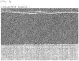
- Example 1 As illustrated in Fig. 2 and Fig. 3 , in Example 1, any pinhole was not observed, whereas in Comparative Example 1, a plurality of pinholes were observed.
- electrodeposition baking is performed by using the electrodeposition coating material simply prepared by using the organic solvent which had a boiling point of higher than or equal to 100°C and was selected by the Hansen solubility parameter, and thus, it was possible to obtain an insulating copper wire including an insulating film which had a dense and smooth surface and high voltage resistance without any pinhole in a safe producing environment.
- the electrodeposition coated article of the present invention in a personal computer, a power inductor for a power source of a smart phone, a transformer of an on-vehicle inverter, and the like.
Landscapes
- Chemical & Material Sciences (AREA)
- Chemical Kinetics & Catalysis (AREA)
- Organic Chemistry (AREA)
- Engineering & Computer Science (AREA)
- Materials Engineering (AREA)
- Electrochemistry (AREA)
- Metallurgy (AREA)
- Life Sciences & Earth Sciences (AREA)
- Wood Science & Technology (AREA)
- Health & Medical Sciences (AREA)
- Molecular Biology (AREA)
- Physics & Mathematics (AREA)
- Spectroscopy & Molecular Physics (AREA)
- Paints Or Removers (AREA)
Applications Claiming Priority (2)
| Application Number | Priority Date | Filing Date | Title |
|---|---|---|---|
| JP2014171210A JP6412740B2 (ja) | 2014-08-26 | 2014-08-26 | 電着塗装体の製造方法 |
| PCT/JP2015/071600 WO2016031480A1 (ja) | 2014-08-26 | 2015-07-30 | 電着塗装体及びその製造方法 |
Publications (3)
| Publication Number | Publication Date |
|---|---|
| EP3187628A1 EP3187628A1 (en) | 2017-07-05 |
| EP3187628A4 EP3187628A4 (en) | 2018-04-04 |
| EP3187628B1 true EP3187628B1 (en) | 2021-03-17 |
Family
ID=55399381
Family Applications (1)
| Application Number | Title | Priority Date | Filing Date |
|---|---|---|---|
| EP15835515.6A Active EP3187628B1 (en) | 2014-08-26 | 2015-07-30 | Electrodeposition coated article and method for producing same |
Country Status (7)
Families Citing this family (2)
| Publication number | Priority date | Publication date | Assignee | Title |
|---|---|---|---|---|
| US11230788B2 (en) | 2016-02-18 | 2022-01-25 | Mitsubishi Materials Corporation | Electrodeposition liquid and electrodeposition-coated article |
| JP6859736B2 (ja) * | 2017-02-16 | 2021-04-14 | 三菱マテリアル株式会社 | 電着液及びこれを用いた絶縁皮膜付き導体の製造方法 |
Family Cites Families (12)
| Publication number | Priority date | Publication date | Assignee | Title |
|---|---|---|---|---|
| JPS5230846A (en) * | 1975-09-03 | 1977-03-08 | Mitsubishi Electric Corp | Method for electrodeposition coating |
| JP2649979B2 (ja) | 1989-11-15 | 1997-09-03 | 三菱電線工業株式会社 | 平角状絶縁電線の製法 |
| JPH07120491B2 (ja) | 1990-02-20 | 1995-12-20 | 三菱電線工業株式会社 | 平角状超薄膜絶縁電線 |
| JPH0465159A (ja) | 1990-07-05 | 1992-03-02 | Oki Electric Ind Co Ltd | キャパシタの製造方法 |
| JP5441802B2 (ja) * | 2009-05-26 | 2014-03-12 | 関西ペイント株式会社 | カチオン電着塗料組成物 |
| JP5449012B2 (ja) * | 2010-05-06 | 2014-03-19 | 古河電気工業株式会社 | 絶縁電線、電気機器及び絶縁電線の製造方法 |
| JPWO2011152364A1 (ja) * | 2010-05-31 | 2013-08-01 | 日立化成株式会社 | 変性ポリアミドイミド樹脂、電気絶縁材料、絶縁層の耐絶縁破壊性向上方法及び絶縁電線 |
| JP5377535B2 (ja) * | 2011-01-31 | 2013-12-25 | 三菱電線工業株式会社 | 絶縁電線の製造方法及び製造装置 |
| JP5609732B2 (ja) * | 2011-03-22 | 2014-10-22 | 日立金属株式会社 | 絶縁塗料及びそれを用いた絶縁電線 |
| US10406791B2 (en) * | 2011-05-12 | 2019-09-10 | Elantas Pdg, Inc. | Composite insulating film |
| WO2013133333A1 (ja) * | 2012-03-07 | 2013-09-12 | 古河電気工業株式会社 | 気泡層入り絶縁電線、電気機器及び気泡層入り絶縁電線の製造方法 |
| JP6069035B2 (ja) * | 2013-03-07 | 2017-01-25 | 三菱マテリアル株式会社 | 電着塗装体の製造方法 |
-
2014
- 2014-08-26 JP JP2014171210A patent/JP6412740B2/ja active Active
-
2015
- 2015-07-30 WO PCT/JP2015/071600 patent/WO2016031480A1/ja active Application Filing
- 2015-07-30 EP EP15835515.6A patent/EP3187628B1/en active Active
- 2015-07-30 CN CN201580038396.1A patent/CN106536792B/zh active Active
- 2015-07-30 KR KR1020177001327A patent/KR102352646B1/ko active Active
- 2015-07-30 US US15/505,157 patent/US20170267874A1/en not_active Abandoned
- 2015-08-10 TW TW104125939A patent/TWI671765B/zh active
Non-Patent Citations (1)
| Title |
|---|
| None * |
Also Published As
| Publication number | Publication date |
|---|---|
| CN106536792A (zh) | 2017-03-22 |
| JP6412740B2 (ja) | 2018-10-24 |
| KR102352646B1 (ko) | 2022-01-17 |
| EP3187628A1 (en) | 2017-07-05 |
| US20170267874A1 (en) | 2017-09-21 |
| TWI671765B (zh) | 2019-09-11 |
| EP3187628A4 (en) | 2018-04-04 |
| TW201611041A (zh) | 2016-03-16 |
| WO2016031480A1 (ja) | 2016-03-03 |
| CN106536792B (zh) | 2019-08-16 |
| KR20170048316A (ko) | 2017-05-08 |
| JP2016044348A (ja) | 2016-04-04 |
Similar Documents
| Publication | Publication Date | Title |
|---|---|---|
| KR102676821B1 (ko) | 전착액 및 전착 도장체 | |
| EP1850353A1 (en) | Conductive film | |
| KR20160096654A (ko) | 도전성 페이스트 및 그것을 사용한 도전막의 제조 방법 | |
| DE102008023882A1 (de) | Druckbare Zusammensetzung auf Basis von Silberpartikeln zur Erzeugung elektrisch leitfähiger Beschichtungen | |
| EP3187628B1 (en) | Electrodeposition coated article and method for producing same | |
| TW201413750A (zh) | 導電膜的製造方法及導電膜形成用組成物 | |
| US12012523B2 (en) | Conductive film formation composition and method for manufacturing conductive film | |
| US8968824B2 (en) | Method for producing silver conductive film | |
| JP6069035B2 (ja) | 電着塗装体の製造方法 | |
| EP3244420A1 (en) | Electroconductive paste and method for manufacturing electroconductive film using same | |
| US11230788B2 (en) | Electrodeposition liquid and electrodeposition-coated article | |
| Ye et al. | Cold plasma welding of polyaniline nanofibers with enhanced electrical and mechanical properties | |
| DE102016202379A1 (de) | Verfahren zur Präparation von Objekten für Untersuchungen mit geladenen Teilchenstrahlen | |
| Fujimto et al. | Flexible multilayer electrode films consisted of polyaniline and polyelectrolyte by layer-by-layer self-assembly | |
| JP2015069752A (ja) | 導電性ペースト、金属薄膜及びその製造方法 | |
| JP2017137541A (ja) | 電着液及びこれを用いた絶縁皮膜の形成方法 | |
| JP2012174375A (ja) | 導電性塗膜の製造方法及び導電性塗膜 | |
| WO2016129518A1 (ja) | 絶縁電線の製造方法 | |
| JP6410278B2 (ja) | 導電膜形成用組成物、および、導電膜の製造方法 | |
| CN114141541B (zh) | 一种电极箔光边成型方法 | |
| JP6869954B2 (ja) | 導電層形成用塗布液、導電層の製造方法及び導電層 | |
| JP6769076B2 (ja) | 電着塗料組成物及びそれを用いた絶縁電線の製造方法 | |
| KR20220148821A (ko) | 저전압 배리스터, 회로 기판, 반도체 부품 패키지 및 인터포저 | |
| 엄태식 et al. | Fabrication of natural melanin nano-particle films byLayer-by-Layer assembly technique |
Legal Events
| Date | Code | Title | Description |
|---|---|---|---|
| STAA | Information on the status of an ep patent application or granted ep patent |
Free format text: STATUS: THE INTERNATIONAL PUBLICATION HAS BEEN MADE |
|
| PUAI | Public reference made under article 153(3) epc to a published international application that has entered the european phase |
Free format text: ORIGINAL CODE: 0009012 |
|
| STAA | Information on the status of an ep patent application or granted ep patent |
Free format text: STATUS: REQUEST FOR EXAMINATION WAS MADE |
|
| 17P | Request for examination filed |
Effective date: 20170126 |
|
| AK | Designated contracting states |
Kind code of ref document: A1 Designated state(s): AL AT BE BG CH CY CZ DE DK EE ES FI FR GB GR HR HU IE IS IT LI LT LU LV MC MK MT NL NO PL PT RO RS SE SI SK SM TR |
|
| AX | Request for extension of the european patent |
Extension state: BA ME |
|
| DAV | Request for validation of the european patent (deleted) | ||
| DAX | Request for extension of the european patent (deleted) | ||
| A4 | Supplementary search report drawn up and despatched |
Effective date: 20180307 |
|
| RIC1 | Information provided on ipc code assigned before grant |
Ipc: C25D 13/04 20060101ALI20180301BHEP Ipc: C25D 13/16 20060101ALI20180301BHEP Ipc: H01B 3/30 20060101ALI20180301BHEP Ipc: C09D 5/44 20060101ALI20180301BHEP Ipc: C25D 13/10 20060101ALI20180301BHEP Ipc: C25D 13/06 20060101AFI20180301BHEP Ipc: C09D 179/08 20060101ALI20180301BHEP |
|
| RAP1 | Party data changed (applicant data changed or rights of an application transferred) |
Owner name: MITSUBISHI MATERIALS CORPORATION Owner name: MITSUBISHI CABLE INDUSTRIES, LTD. |
|
| RAP1 | Party data changed (applicant data changed or rights of an application transferred) |
Owner name: MITSUBISHI MATERIALS CORPORATION |
|
| STAA | Information on the status of an ep patent application or granted ep patent |
Free format text: STATUS: EXAMINATION IS IN PROGRESS |
|
| 17Q | First examination report despatched |
Effective date: 20200817 |
|
| GRAP | Despatch of communication of intention to grant a patent |
Free format text: ORIGINAL CODE: EPIDOSNIGR1 |
|
| STAA | Information on the status of an ep patent application or granted ep patent |
Free format text: STATUS: GRANT OF PATENT IS INTENDED |
|
| INTG | Intention to grant announced |
Effective date: 20201120 |
|
| GRAS | Grant fee paid |
Free format text: ORIGINAL CODE: EPIDOSNIGR3 |
|
| GRAA | (expected) grant |
Free format text: ORIGINAL CODE: 0009210 |
|
| STAA | Information on the status of an ep patent application or granted ep patent |
Free format text: STATUS: THE PATENT HAS BEEN GRANTED |
|
| AK | Designated contracting states |
Kind code of ref document: B1 Designated state(s): AL AT BE BG CH CY CZ DE DK EE ES FI FR GB GR HR HU IE IS IT LI LT LU LV MC MK MT NL NO PL PT RO RS SE SI SK SM TR |
|
| REG | Reference to a national code |
Ref country code: GB Ref legal event code: FG4D |
|
| REG | Reference to a national code |
Ref country code: CH Ref legal event code: EP |
|
| REG | Reference to a national code |
Ref country code: DE Ref legal event code: R096 Ref document number: 602015067064 Country of ref document: DE |
|
| REG | Reference to a national code |
Ref country code: IE Ref legal event code: FG4D |
|
| REG | Reference to a national code |
Ref country code: AT Ref legal event code: REF Ref document number: 1372325 Country of ref document: AT Kind code of ref document: T Effective date: 20210415 |
|
| REG | Reference to a national code |
Ref country code: LT Ref legal event code: MG9D |
|
| PG25 | Lapsed in a contracting state [announced via postgrant information from national office to epo] |
Ref country code: NO Free format text: LAPSE BECAUSE OF FAILURE TO SUBMIT A TRANSLATION OF THE DESCRIPTION OR TO PAY THE FEE WITHIN THE PRESCRIBED TIME-LIMIT Effective date: 20210617 Ref country code: FI Free format text: LAPSE BECAUSE OF FAILURE TO SUBMIT A TRANSLATION OF THE DESCRIPTION OR TO PAY THE FEE WITHIN THE PRESCRIBED TIME-LIMIT Effective date: 20210317 Ref country code: HR Free format text: LAPSE BECAUSE OF FAILURE TO SUBMIT A TRANSLATION OF THE DESCRIPTION OR TO PAY THE FEE WITHIN THE PRESCRIBED TIME-LIMIT Effective date: 20210317 Ref country code: GR Free format text: LAPSE BECAUSE OF FAILURE TO SUBMIT A TRANSLATION OF THE DESCRIPTION OR TO PAY THE FEE WITHIN THE PRESCRIBED TIME-LIMIT Effective date: 20210618 Ref country code: BG Free format text: LAPSE BECAUSE OF FAILURE TO SUBMIT A TRANSLATION OF THE DESCRIPTION OR TO PAY THE FEE WITHIN THE PRESCRIBED TIME-LIMIT Effective date: 20210617 |
|
| REG | Reference to a national code |
Ref country code: AT Ref legal event code: MK05 Ref document number: 1372325 Country of ref document: AT Kind code of ref document: T Effective date: 20210317 |
|
| REG | Reference to a national code |
Ref country code: NL Ref legal event code: MP Effective date: 20210317 |
|
| PG25 | Lapsed in a contracting state [announced via postgrant information from national office to epo] |
Ref country code: LV Free format text: LAPSE BECAUSE OF FAILURE TO SUBMIT A TRANSLATION OF THE DESCRIPTION OR TO PAY THE FEE WITHIN THE PRESCRIBED TIME-LIMIT Effective date: 20210317 Ref country code: RS Free format text: LAPSE BECAUSE OF FAILURE TO SUBMIT A TRANSLATION OF THE DESCRIPTION OR TO PAY THE FEE WITHIN THE PRESCRIBED TIME-LIMIT Effective date: 20210317 Ref country code: SE Free format text: LAPSE BECAUSE OF FAILURE TO SUBMIT A TRANSLATION OF THE DESCRIPTION OR TO PAY THE FEE WITHIN THE PRESCRIBED TIME-LIMIT Effective date: 20210317 |
|
| PG25 | Lapsed in a contracting state [announced via postgrant information from national office to epo] |
Ref country code: NL Free format text: LAPSE BECAUSE OF FAILURE TO SUBMIT A TRANSLATION OF THE DESCRIPTION OR TO PAY THE FEE WITHIN THE PRESCRIBED TIME-LIMIT Effective date: 20210317 |
|
| PG25 | Lapsed in a contracting state [announced via postgrant information from national office to epo] |
Ref country code: LT Free format text: LAPSE BECAUSE OF FAILURE TO SUBMIT A TRANSLATION OF THE DESCRIPTION OR TO PAY THE FEE WITHIN THE PRESCRIBED TIME-LIMIT Effective date: 20210317 Ref country code: CZ Free format text: LAPSE BECAUSE OF FAILURE TO SUBMIT A TRANSLATION OF THE DESCRIPTION OR TO PAY THE FEE WITHIN THE PRESCRIBED TIME-LIMIT Effective date: 20210317 Ref country code: EE Free format text: LAPSE BECAUSE OF FAILURE TO SUBMIT A TRANSLATION OF THE DESCRIPTION OR TO PAY THE FEE WITHIN THE PRESCRIBED TIME-LIMIT Effective date: 20210317 Ref country code: AT Free format text: LAPSE BECAUSE OF FAILURE TO SUBMIT A TRANSLATION OF THE DESCRIPTION OR TO PAY THE FEE WITHIN THE PRESCRIBED TIME-LIMIT Effective date: 20210317 Ref country code: SM Free format text: LAPSE BECAUSE OF FAILURE TO SUBMIT A TRANSLATION OF THE DESCRIPTION OR TO PAY THE FEE WITHIN THE PRESCRIBED TIME-LIMIT Effective date: 20210317 |
|
| PG25 | Lapsed in a contracting state [announced via postgrant information from national office to epo] |
Ref country code: PL Free format text: LAPSE BECAUSE OF FAILURE TO SUBMIT A TRANSLATION OF THE DESCRIPTION OR TO PAY THE FEE WITHIN THE PRESCRIBED TIME-LIMIT Effective date: 20210317 Ref country code: PT Free format text: LAPSE BECAUSE OF FAILURE TO SUBMIT A TRANSLATION OF THE DESCRIPTION OR TO PAY THE FEE WITHIN THE PRESCRIBED TIME-LIMIT Effective date: 20210719 Ref country code: SK Free format text: LAPSE BECAUSE OF FAILURE TO SUBMIT A TRANSLATION OF THE DESCRIPTION OR TO PAY THE FEE WITHIN THE PRESCRIBED TIME-LIMIT Effective date: 20210317 Ref country code: RO Free format text: LAPSE BECAUSE OF FAILURE TO SUBMIT A TRANSLATION OF THE DESCRIPTION OR TO PAY THE FEE WITHIN THE PRESCRIBED TIME-LIMIT Effective date: 20210317 Ref country code: IS Free format text: LAPSE BECAUSE OF FAILURE TO SUBMIT A TRANSLATION OF THE DESCRIPTION OR TO PAY THE FEE WITHIN THE PRESCRIBED TIME-LIMIT Effective date: 20210717 |
|
| REG | Reference to a national code |
Ref country code: DE Ref legal event code: R097 Ref document number: 602015067064 Country of ref document: DE |
|
| PLBE | No opposition filed within time limit |
Free format text: ORIGINAL CODE: 0009261 |
|
| STAA | Information on the status of an ep patent application or granted ep patent |
Free format text: STATUS: NO OPPOSITION FILED WITHIN TIME LIMIT |
|
| PG25 | Lapsed in a contracting state [announced via postgrant information from national office to epo] |
Ref country code: AL Free format text: LAPSE BECAUSE OF FAILURE TO SUBMIT A TRANSLATION OF THE DESCRIPTION OR TO PAY THE FEE WITHIN THE PRESCRIBED TIME-LIMIT Effective date: 20210317 Ref country code: ES Free format text: LAPSE BECAUSE OF FAILURE TO SUBMIT A TRANSLATION OF THE DESCRIPTION OR TO PAY THE FEE WITHIN THE PRESCRIBED TIME-LIMIT Effective date: 20210317 Ref country code: DK Free format text: LAPSE BECAUSE OF FAILURE TO SUBMIT A TRANSLATION OF THE DESCRIPTION OR TO PAY THE FEE WITHIN THE PRESCRIBED TIME-LIMIT Effective date: 20210317 |
|
| 26N | No opposition filed |
Effective date: 20211220 |
|
| PG25 | Lapsed in a contracting state [announced via postgrant information from national office to epo] |
Ref country code: SI Free format text: LAPSE BECAUSE OF FAILURE TO SUBMIT A TRANSLATION OF THE DESCRIPTION OR TO PAY THE FEE WITHIN THE PRESCRIBED TIME-LIMIT Effective date: 20210317 |
|
| REG | Reference to a national code |
Ref country code: CH Ref legal event code: PL |
|
| PG25 | Lapsed in a contracting state [announced via postgrant information from national office to epo] |
Ref country code: MC Free format text: LAPSE BECAUSE OF FAILURE TO SUBMIT A TRANSLATION OF THE DESCRIPTION OR TO PAY THE FEE WITHIN THE PRESCRIBED TIME-LIMIT Effective date: 20210317 |
|
| REG | Reference to a national code |
Ref country code: BE Ref legal event code: MM Effective date: 20210731 |
|
| PG25 | Lapsed in a contracting state [announced via postgrant information from national office to epo] |
Ref country code: LI Free format text: LAPSE BECAUSE OF NON-PAYMENT OF DUE FEES Effective date: 20210731 Ref country code: IT Free format text: LAPSE BECAUSE OF FAILURE TO SUBMIT A TRANSLATION OF THE DESCRIPTION OR TO PAY THE FEE WITHIN THE PRESCRIBED TIME-LIMIT Effective date: 20210317 Ref country code: CH Free format text: LAPSE BECAUSE OF NON-PAYMENT OF DUE FEES Effective date: 20210731 |
|
| PG25 | Lapsed in a contracting state [announced via postgrant information from national office to epo] |
Ref country code: IS Free format text: LAPSE BECAUSE OF FAILURE TO SUBMIT A TRANSLATION OF THE DESCRIPTION OR TO PAY THE FEE WITHIN THE PRESCRIBED TIME-LIMIT Effective date: 20210717 Ref country code: LU Free format text: LAPSE BECAUSE OF NON-PAYMENT OF DUE FEES Effective date: 20210730 |
|
| PG25 | Lapsed in a contracting state [announced via postgrant information from national office to epo] |
Ref country code: IE Free format text: LAPSE BECAUSE OF NON-PAYMENT OF DUE FEES Effective date: 20210730 Ref country code: BE Free format text: LAPSE BECAUSE OF NON-PAYMENT OF DUE FEES Effective date: 20210731 |
|
| PG25 | Lapsed in a contracting state [announced via postgrant information from national office to epo] |
Ref country code: HU Free format text: LAPSE BECAUSE OF FAILURE TO SUBMIT A TRANSLATION OF THE DESCRIPTION OR TO PAY THE FEE WITHIN THE PRESCRIBED TIME-LIMIT; INVALID AB INITIO Effective date: 20150730 |
|
| PG25 | Lapsed in a contracting state [announced via postgrant information from national office to epo] |
Ref country code: CY Free format text: LAPSE BECAUSE OF FAILURE TO SUBMIT A TRANSLATION OF THE DESCRIPTION OR TO PAY THE FEE WITHIN THE PRESCRIBED TIME-LIMIT Effective date: 20210317 |
|
| PG25 | Lapsed in a contracting state [announced via postgrant information from national office to epo] |
Ref country code: MK Free format text: LAPSE BECAUSE OF FAILURE TO SUBMIT A TRANSLATION OF THE DESCRIPTION OR TO PAY THE FEE WITHIN THE PRESCRIBED TIME-LIMIT Effective date: 20210317 |
|
| PG25 | Lapsed in a contracting state [announced via postgrant information from national office to epo] |
Ref country code: TR Free format text: LAPSE BECAUSE OF FAILURE TO SUBMIT A TRANSLATION OF THE DESCRIPTION OR TO PAY THE FEE WITHIN THE PRESCRIBED TIME-LIMIT Effective date: 20210317 |
|
| PG25 | Lapsed in a contracting state [announced via postgrant information from national office to epo] |
Ref country code: MT Free format text: LAPSE BECAUSE OF FAILURE TO SUBMIT A TRANSLATION OF THE DESCRIPTION OR TO PAY THE FEE WITHIN THE PRESCRIBED TIME-LIMIT Effective date: 20210317 |
|
| PGFP | Annual fee paid to national office [announced via postgrant information from national office to epo] |
Ref country code: DE Payment date: 20240719 Year of fee payment: 10 |
|
| PGFP | Annual fee paid to national office [announced via postgrant information from national office to epo] |
Ref country code: GB Payment date: 20240725 Year of fee payment: 10 |
|
| PGFP | Annual fee paid to national office [announced via postgrant information from national office to epo] |
Ref country code: FR Payment date: 20240730 Year of fee payment: 10 |