EP3175496B1 - Mise en motifs photolithographique de dispositifs électroniques organiques - Google Patents
Mise en motifs photolithographique de dispositifs électroniques organiques Download PDFInfo
- Publication number
- EP3175496B1 EP3175496B1 EP15828065.1A EP15828065A EP3175496B1 EP 3175496 B1 EP3175496 B1 EP 3175496B1 EP 15828065 A EP15828065 A EP 15828065A EP 3175496 B1 EP3175496 B1 EP 3175496B1
- Authority
- EP
- European Patent Office
- Prior art keywords
- lift
- organic
- layer
- fluorinated
- layers
- Prior art date
- Legal status (The legal status is an assumption and is not a legal conclusion. Google has not performed a legal analysis and makes no representation as to the accuracy of the status listed.)
- Active
Links
- 238000000059 patterning Methods 0.000 title description 18
- 239000000463 material Substances 0.000 claims description 161
- 229920002120 photoresistant polymer Polymers 0.000 claims description 77
- 239000002904 solvent Substances 0.000 claims description 67
- 239000000758 substrate Substances 0.000 claims description 55
- 238000000151 deposition Methods 0.000 claims description 40
- 238000000034 method Methods 0.000 claims description 40
- 239000003795 chemical substances by application Substances 0.000 claims description 37
- 239000000203 mixture Substances 0.000 claims description 25
- 230000015572 biosynthetic process Effects 0.000 claims description 13
- 239000011248 coating agent Substances 0.000 claims description 13
- 238000000576 coating method Methods 0.000 claims description 13
- 230000005855 radiation Effects 0.000 claims description 13
- 239000012459 cleaning agent Substances 0.000 claims description 12
- 238000011282 treatment Methods 0.000 claims description 11
- 238000004140 cleaning Methods 0.000 claims description 9
- 239000000126 substance Substances 0.000 claims description 6
- 238000004519 manufacturing process Methods 0.000 claims description 5
- 238000003384 imaging method Methods 0.000 claims description 4
- 239000010410 layer Substances 0.000 description 362
- 239000002585 base Substances 0.000 description 45
- 239000011368 organic material Substances 0.000 description 32
- 230000008021 deposition Effects 0.000 description 24
- 229920001621 AMOLED Polymers 0.000 description 21
- 229910052751 metal Inorganic materials 0.000 description 21
- 239000002184 metal Substances 0.000 description 21
- 229920002313 fluoropolymer Polymers 0.000 description 19
- XLYOFNOQVPJJNP-UHFFFAOYSA-N water Substances O XLYOFNOQVPJJNP-UHFFFAOYSA-N 0.000 description 15
- QVGXLLKOCUKJST-UHFFFAOYSA-N atomic oxygen Chemical compound [O] QVGXLLKOCUKJST-UHFFFAOYSA-N 0.000 description 14
- 239000002019 doping agent Substances 0.000 description 14
- 239000001301 oxygen Substances 0.000 description 14
- 229910052760 oxygen Inorganic materials 0.000 description 14
- 239000004811 fluoropolymer Substances 0.000 description 13
- 238000012545 processing Methods 0.000 description 13
- IJGRMHOSHXDMSA-UHFFFAOYSA-N Atomic nitrogen Chemical compound N#N IJGRMHOSHXDMSA-UHFFFAOYSA-N 0.000 description 12
- 239000000243 solution Substances 0.000 description 11
- -1 gallium nitride Chemical class 0.000 description 9
- 238000007740 vapor deposition Methods 0.000 description 9
- 230000006378 damage Effects 0.000 description 8
- 238000005530 etching Methods 0.000 description 8
- 239000002356 single layer Substances 0.000 description 8
- YCKRFDGAMUMZLT-UHFFFAOYSA-N Fluorine atom Chemical compound [F] YCKRFDGAMUMZLT-UHFFFAOYSA-N 0.000 description 7
- 238000003491 array Methods 0.000 description 7
- 239000004020 conductor Substances 0.000 description 7
- DKHNGUNXLDCATP-UHFFFAOYSA-N dipyrazino[2,3-f:2',3'-h]quinoxaline-2,3,6,7,10,11-hexacarbonitrile Chemical compound C12=NC(C#N)=C(C#N)N=C2C2=NC(C#N)=C(C#N)N=C2C2=C1N=C(C#N)C(C#N)=N2 DKHNGUNXLDCATP-UHFFFAOYSA-N 0.000 description 7
- 239000011737 fluorine Substances 0.000 description 7
- 229910052731 fluorine Inorganic materials 0.000 description 7
- 239000007789 gas Substances 0.000 description 7
- 230000008569 process Effects 0.000 description 7
- 239000004065 semiconductor Substances 0.000 description 7
- 229910052783 alkali metal Inorganic materials 0.000 description 6
- 150000001340 alkali metals Chemical class 0.000 description 6
- 230000008901 benefit Effects 0.000 description 6
- 238000011161 development Methods 0.000 description 6
- 238000002347 injection Methods 0.000 description 6
- 239000007924 injection Substances 0.000 description 6
- 229910044991 metal oxide Inorganic materials 0.000 description 6
- 150000004706 metal oxides Chemical class 0.000 description 6
- 229910052757 nitrogen Inorganic materials 0.000 description 6
- 230000001590 oxidative effect Effects 0.000 description 6
- 238000000926 separation method Methods 0.000 description 6
- QKAGYSDHEJITFV-UHFFFAOYSA-N 1,1,1,2,2,3,4,5,5,5-decafluoro-3-methoxy-4-(trifluoromethyl)pentane Chemical compound FC(F)(F)C(F)(F)C(F)(OC)C(F)(C(F)(F)F)C(F)(F)F QKAGYSDHEJITFV-UHFFFAOYSA-N 0.000 description 5
- UFHFLCQGNIYNRP-UHFFFAOYSA-N Hydrogen Chemical compound [H][H] UFHFLCQGNIYNRP-UHFFFAOYSA-N 0.000 description 5
- 229910052782 aluminium Inorganic materials 0.000 description 5
- XAGFODPZIPBFFR-UHFFFAOYSA-N aluminium Chemical compound [Al] XAGFODPZIPBFFR-UHFFFAOYSA-N 0.000 description 5
- 239000010406 cathode material Substances 0.000 description 5
- 239000003086 colorant Substances 0.000 description 5
- 230000007547 defect Effects 0.000 description 5
- 239000007772 electrode material Substances 0.000 description 5
- 239000011521 glass Substances 0.000 description 5
- 239000001257 hydrogen Substances 0.000 description 5
- 229910052739 hydrogen Inorganic materials 0.000 description 5
- 239000012044 organic layer Substances 0.000 description 5
- YTPLMLYBLZKORZ-UHFFFAOYSA-N Thiophene Chemical compound C=1C=CSC=1 YTPLMLYBLZKORZ-UHFFFAOYSA-N 0.000 description 4
- 239000002318 adhesion promoter Substances 0.000 description 4
- 229910052784 alkaline earth metal Inorganic materials 0.000 description 4
- 150000001342 alkaline earth metals Chemical class 0.000 description 4
- 230000004888 barrier function Effects 0.000 description 4
- 239000003054 catalyst Substances 0.000 description 4
- 230000002950 deficient Effects 0.000 description 4
- 238000001312 dry etching Methods 0.000 description 4
- 238000001035 drying Methods 0.000 description 4
- 229910052741 iridium Inorganic materials 0.000 description 4
- GKOZUEZYRPOHIO-UHFFFAOYSA-N iridium atom Chemical compound [Ir] GKOZUEZYRPOHIO-UHFFFAOYSA-N 0.000 description 4
- 125000005647 linker group Chemical group 0.000 description 4
- BASFCYQUMIYNBI-UHFFFAOYSA-N platinum Chemical compound [Pt] BASFCYQUMIYNBI-UHFFFAOYSA-N 0.000 description 4
- 229920000642 polymer Polymers 0.000 description 4
- 239000003586 protic polar solvent Substances 0.000 description 4
- 239000007787 solid Substances 0.000 description 4
- 125000000217 alkyl group Chemical group 0.000 description 3
- 239000010405 anode material Substances 0.000 description 3
- 239000012620 biological material Substances 0.000 description 3
- 239000002131 composite material Substances 0.000 description 3
- 230000032798 delamination Effects 0.000 description 3
- 239000001307 helium Substances 0.000 description 3
- 229910052734 helium Inorganic materials 0.000 description 3
- SWQJXJOGLNCZEY-UHFFFAOYSA-N helium atom Chemical compound [He] SWQJXJOGLNCZEY-UHFFFAOYSA-N 0.000 description 3
- 229910010272 inorganic material Inorganic materials 0.000 description 3
- 238000010884 ion-beam technique Methods 0.000 description 3
- 239000007788 liquid Substances 0.000 description 3
- 150000002739 metals Chemical class 0.000 description 3
- 239000013110 organic ligand Substances 0.000 description 3
- 230000035515 penetration Effects 0.000 description 3
- NOPJRYAFUXTDLX-UHFFFAOYSA-N 1,1,1,2,2,3,3-heptafluoro-3-methoxypropane Chemical compound COC(F)(F)C(F)(F)C(F)(F)F NOPJRYAFUXTDLX-UHFFFAOYSA-N 0.000 description 2
- WVRJJXQSRCWPNS-UHFFFAOYSA-N 1,1,2,2-tetrafluoro-1-[2-(1,1,2,2-tetrafluoroethoxy)ethoxy]ethane Chemical compound FC(F)C(F)(F)OCCOC(F)(F)C(F)F WVRJJXQSRCWPNS-UHFFFAOYSA-N 0.000 description 2
- DFUYAWQUODQGFF-UHFFFAOYSA-N 1-ethoxy-1,1,2,2,3,3,4,4,4-nonafluorobutane Chemical compound CCOC(F)(F)C(F)(F)C(F)(F)C(F)(F)F DFUYAWQUODQGFF-UHFFFAOYSA-N 0.000 description 2
- IXHWGNYCZPISET-UHFFFAOYSA-N 2-[4-(dicyanomethylidene)-2,3,5,6-tetrafluorocyclohexa-2,5-dien-1-ylidene]propanedinitrile Chemical compound FC1=C(F)C(=C(C#N)C#N)C(F)=C(F)C1=C(C#N)C#N IXHWGNYCZPISET-UHFFFAOYSA-N 0.000 description 2
- HHBBIOLEJRWIGU-UHFFFAOYSA-N 4-ethoxy-1,1,1,2,2,3,3,4,5,6,6,6-dodecafluoro-5-(trifluoromethyl)hexane Chemical compound CCOC(F)(C(F)(C(F)(F)F)C(F)(F)F)C(F)(F)C(F)(F)C(F)(F)F HHBBIOLEJRWIGU-UHFFFAOYSA-N 0.000 description 2
- OSQXTXTYKAEHQV-WXUKJITCSA-N 4-methyl-n-[4-[(e)-2-[4-[4-[(e)-2-[4-(4-methyl-n-(4-methylphenyl)anilino)phenyl]ethenyl]phenyl]phenyl]ethenyl]phenyl]-n-(4-methylphenyl)aniline Chemical compound C1=CC(C)=CC=C1N(C=1C=CC(\C=C\C=2C=CC(=CC=2)C=2C=CC(\C=C\C=3C=CC(=CC=3)N(C=3C=CC(C)=CC=3)C=3C=CC(C)=CC=3)=CC=2)=CC=1)C1=CC=C(C)C=C1 OSQXTXTYKAEHQV-WXUKJITCSA-N 0.000 description 2
- UJOBWOGCFQCDNV-UHFFFAOYSA-N 9H-carbazole Chemical compound C1=CC=C2C3=CC=CC=C3NC2=C1 UJOBWOGCFQCDNV-UHFFFAOYSA-N 0.000 description 2
- XKRFYHLGVUSROY-UHFFFAOYSA-N Argon Chemical compound [Ar] XKRFYHLGVUSROY-UHFFFAOYSA-N 0.000 description 2
- LFQSCWFLJHTTHZ-UHFFFAOYSA-N Ethanol Chemical compound CCO LFQSCWFLJHTTHZ-UHFFFAOYSA-N 0.000 description 2
- 229910001111 Fine metal Inorganic materials 0.000 description 2
- ZOKXTWBITQBERF-UHFFFAOYSA-N Molybdenum Chemical compound [Mo] ZOKXTWBITQBERF-UHFFFAOYSA-N 0.000 description 2
- KDLHZDBZIXYQEI-UHFFFAOYSA-N Palladium Chemical compound [Pd] KDLHZDBZIXYQEI-UHFFFAOYSA-N 0.000 description 2
- XLOMVQKBTHCTTD-UHFFFAOYSA-N Zinc monoxide Chemical compound [Zn]=O XLOMVQKBTHCTTD-UHFFFAOYSA-N 0.000 description 2
- 239000011358 absorbing material Substances 0.000 description 2
- CUJRVFIICFDLGR-UHFFFAOYSA-N acetylacetonate Chemical compound CC(=O)[CH-]C(C)=O CUJRVFIICFDLGR-UHFFFAOYSA-N 0.000 description 2
- 230000009471 action Effects 0.000 description 2
- 239000011149 active material Substances 0.000 description 2
- 238000013019 agitation Methods 0.000 description 2
- 150000004982 aromatic amines Chemical group 0.000 description 2
- 239000000919 ceramic Substances 0.000 description 2
- 150000001875 compounds Chemical class 0.000 description 2
- 238000011109 contamination Methods 0.000 description 2
- 238000007796 conventional method Methods 0.000 description 2
- 238000004132 cross linking Methods 0.000 description 2
- 238000010586 diagram Methods 0.000 description 2
- 238000005516 engineering process Methods 0.000 description 2
- 238000001704 evaporation Methods 0.000 description 2
- 230000008020 evaporation Effects 0.000 description 2
- 239000010408 film Substances 0.000 description 2
- 235000011194 food seasoning agent Nutrition 0.000 description 2
- PCHJSUWPFVWCPO-UHFFFAOYSA-N gold Chemical compound [Au] PCHJSUWPFVWCPO-UHFFFAOYSA-N 0.000 description 2
- 229910052737 gold Inorganic materials 0.000 description 2
- 239000010931 gold Substances 0.000 description 2
- AMGQUBHHOARCQH-UHFFFAOYSA-N indium;oxotin Chemical compound [In].[Sn]=O AMGQUBHHOARCQH-UHFFFAOYSA-N 0.000 description 2
- 230000001939 inductive effect Effects 0.000 description 2
- 239000011147 inorganic material Substances 0.000 description 2
- 239000011159 matrix material Substances 0.000 description 2
- 229910052750 molybdenum Inorganic materials 0.000 description 2
- 239000011733 molybdenum Substances 0.000 description 2
- 239000002105 nanoparticle Substances 0.000 description 2
- 150000004767 nitrides Chemical class 0.000 description 2
- 150000007524 organic acids Chemical class 0.000 description 2
- 239000003960 organic solvent Substances 0.000 description 2
- 229910052697 platinum Inorganic materials 0.000 description 2
- 238000000992 sputter etching Methods 0.000 description 2
- 230000008961 swelling Effects 0.000 description 2
- 239000010409 thin film Substances 0.000 description 2
- 229930192474 thiophene Natural products 0.000 description 2
- 238000012546 transfer Methods 0.000 description 2
- 239000012808 vapor phase Substances 0.000 description 2
- YVTHLONGBIQYBO-UHFFFAOYSA-N zinc indium(3+) oxygen(2-) Chemical compound [O--].[Zn++].[In+3] YVTHLONGBIQYBO-UHFFFAOYSA-N 0.000 description 2
- PFNQVRZLDWYSCW-UHFFFAOYSA-N (fluoren-9-ylideneamino) n-naphthalen-1-ylcarbamate Chemical compound C12=CC=CC=C2C2=CC=CC=C2C1=NOC(=O)NC1=CC=CC2=CC=CC=C12 PFNQVRZLDWYSCW-UHFFFAOYSA-N 0.000 description 1
- OBQBCHMEIBSHBO-UHFFFAOYSA-N 1,1,1,2,2,3,3,4,4,5,5,6,6-tridecafluoro-8-propoxyoctane Chemical compound CCCOCCC(F)(F)C(F)(F)C(F)(F)C(F)(F)C(F)(F)C(F)(F)F OBQBCHMEIBSHBO-UHFFFAOYSA-N 0.000 description 1
- ZNBGTBKGFZMWKR-UHFFFAOYSA-N 1,1,2,2,3,3,4,4-octafluoro-5-(1,1,2,2-tetrafluoroethoxy)pentane Chemical compound FC(F)C(F)(F)OCC(F)(F)C(F)(F)C(F)(F)C(F)F ZNBGTBKGFZMWKR-UHFFFAOYSA-N 0.000 description 1
- HCBRSIIGBBDDCD-UHFFFAOYSA-N 1,1,2,2-tetrafluoro-3-(1,1,2,2-tetrafluoroethoxy)propane Chemical compound FC(F)C(F)(F)COC(F)(F)C(F)F HCBRSIIGBBDDCD-UHFFFAOYSA-N 0.000 description 1
- SQEGLLMNIBLLNQ-UHFFFAOYSA-N 1-ethoxy-1,1,2,3,3,3-hexafluoro-2-(trifluoromethyl)propane Chemical compound CCOC(F)(F)C(F)(C(F)(F)F)C(F)(F)F SQEGLLMNIBLLNQ-UHFFFAOYSA-N 0.000 description 1
- YRGYOFYTTFLPQM-UHFFFAOYSA-N 2,3,3,4,4-pentafluoro-2,5-bis(1,1,1,2,3,3,3-heptafluoropropan-2-yl)-5-methoxyoxolane Chemical compound COC1(OC(F)(C(F)(C(F)(F)F)C(F)(F)F)C(F)(F)C1(F)F)C(F)(C(F)(F)F)C(F)(F)F YRGYOFYTTFLPQM-UHFFFAOYSA-N 0.000 description 1
- DJXNLVJQMJNEMN-UHFFFAOYSA-N 2-[difluoro(methoxy)methyl]-1,1,1,2,3,3,3-heptafluoropropane Chemical compound COC(F)(F)C(F)(C(F)(F)F)C(F)(F)F DJXNLVJQMJNEMN-UHFFFAOYSA-N 0.000 description 1
- FNUBKINEQIEODM-UHFFFAOYSA-N 3,3,4,4,5,5,5-heptafluoropentanal Chemical compound FC(F)(F)C(F)(F)C(F)(F)CC=O FNUBKINEQIEODM-UHFFFAOYSA-N 0.000 description 1
- DMEVMYSQZPJFOK-UHFFFAOYSA-N 3,4,5,6,9,10-hexazatetracyclo[12.4.0.02,7.08,13]octadeca-1(18),2(7),3,5,8(13),9,11,14,16-nonaene Chemical group N1=NN=C2C3=CC=CC=C3C3=CC=NN=C3C2=N1 DMEVMYSQZPJFOK-UHFFFAOYSA-N 0.000 description 1
- YFCSASDLEBELEU-UHFFFAOYSA-N 3,4,5,6,9,10-hexazatetracyclo[12.4.0.02,7.08,13]octadeca-1(18),2(7),3,5,8(13),9,11,14,16-nonaene-11,12,15,16,17,18-hexacarbonitrile Chemical group N#CC1=C(C#N)C(C#N)=C2C3=C(C#N)C(C#N)=NN=C3C3=NN=NN=C3C2=C1C#N YFCSASDLEBELEU-UHFFFAOYSA-N 0.000 description 1
- JNGDCMHTNXRQQD-UHFFFAOYSA-N 3,6-dioxocyclohexa-1,4-diene-1,2,4,5-tetracarbonitrile Chemical class O=C1C(C#N)=C(C#N)C(=O)C(C#N)=C1C#N JNGDCMHTNXRQQD-UHFFFAOYSA-N 0.000 description 1
- OKTJSMMVPCPJKN-UHFFFAOYSA-N Carbon Chemical compound [C] OKTJSMMVPCPJKN-UHFFFAOYSA-N 0.000 description 1
- 206010073306 Exposure to radiation Diseases 0.000 description 1
- 229910002601 GaN Inorganic materials 0.000 description 1
- JMASRVWKEDWRBT-UHFFFAOYSA-N Gallium nitride Chemical compound [Ga]#N JMASRVWKEDWRBT-UHFFFAOYSA-N 0.000 description 1
- 229910021578 Iron(III) chloride Inorganic materials 0.000 description 1
- FYYHWMGAXLPEAU-UHFFFAOYSA-N Magnesium Chemical compound [Mg] FYYHWMGAXLPEAU-UHFFFAOYSA-N 0.000 description 1
- CERQOIWHTDAKMF-UHFFFAOYSA-M Methacrylate Chemical compound CC(=C)C([O-])=O CERQOIWHTDAKMF-UHFFFAOYSA-M 0.000 description 1
- CBENFWSGALASAD-UHFFFAOYSA-N Ozone Chemical compound [O-][O+]=O CBENFWSGALASAD-UHFFFAOYSA-N 0.000 description 1
- 229920006926 PFC Polymers 0.000 description 1
- 206010034972 Photosensitivity reaction Diseases 0.000 description 1
- BQCADISMDOOEFD-UHFFFAOYSA-N Silver Chemical compound [Ag] BQCADISMDOOEFD-UHFFFAOYSA-N 0.000 description 1
- 239000005083 Zinc sulfide Substances 0.000 description 1
- GENZLHCFIPDZNJ-UHFFFAOYSA-N [In+3].[O-2].[Mg+2] Chemical compound [In+3].[O-2].[Mg+2] GENZLHCFIPDZNJ-UHFFFAOYSA-N 0.000 description 1
- 239000002253 acid Substances 0.000 description 1
- 239000003513 alkali Substances 0.000 description 1
- IUFDZNVMARBLOJ-UHFFFAOYSA-K aluminum;quinoline-2-carboxylate Chemical class [Al+3].C1=CC=CC2=NC(C(=O)[O-])=CC=C21.C1=CC=CC2=NC(C(=O)[O-])=CC=C21.C1=CC=CC2=NC(C(=O)[O-])=CC=C21 IUFDZNVMARBLOJ-UHFFFAOYSA-K 0.000 description 1
- 150000001454 anthracenes Chemical class 0.000 description 1
- 239000007864 aqueous solution Substances 0.000 description 1
- 229910052786 argon Inorganic materials 0.000 description 1
- HFACYLZERDEVSX-UHFFFAOYSA-N benzidine Chemical compound C1=CC(N)=CC=C1C1=CC=C(N)C=C1 HFACYLZERDEVSX-UHFFFAOYSA-N 0.000 description 1
- 150000001556 benzimidazoles Chemical class 0.000 description 1
- UORVGPXVDQYIDP-BJUDXGSMSA-N borane Chemical class [10BH3] UORVGPXVDQYIDP-BJUDXGSMSA-N 0.000 description 1
- 239000006227 byproduct Substances 0.000 description 1
- 239000003990 capacitor Substances 0.000 description 1
- 150000001716 carbazoles Chemical class 0.000 description 1
- 150000001732 carboxylic acid derivatives Chemical class 0.000 description 1
- 239000012159 carrier gas Substances 0.000 description 1
- 239000003518 caustics Substances 0.000 description 1
- 238000012668 chain scission Methods 0.000 description 1
- 238000003486 chemical etching Methods 0.000 description 1
- 238000005229 chemical vapour deposition Methods 0.000 description 1
- 239000008199 coating composition Substances 0.000 description 1
- 230000000052 comparative effect Effects 0.000 description 1
- 230000000295 complement effect Effects 0.000 description 1
- 239000000356 contaminant Substances 0.000 description 1
- 150000004696 coordination complex Chemical class 0.000 description 1
- 238000001723 curing Methods 0.000 description 1
- 238000013461 design Methods 0.000 description 1
- 239000003989 dielectric material Substances 0.000 description 1
- 238000004090 dissolution Methods 0.000 description 1
- 230000000694 effects Effects 0.000 description 1
- 238000005441 electronic device fabrication Methods 0.000 description 1
- 239000012776 electronic material Substances 0.000 description 1
- 230000002708 enhancing effect Effects 0.000 description 1
- 238000001914 filtration Methods 0.000 description 1
- 229910021389 graphene Inorganic materials 0.000 description 1
- 238000003306 harvesting Methods 0.000 description 1
- 230000005525 hole transport Effects 0.000 description 1
- 238000007654 immersion Methods 0.000 description 1
- 239000011261 inert gas Substances 0.000 description 1
- 150000002484 inorganic compounds Chemical class 0.000 description 1
- 230000003993 interaction Effects 0.000 description 1
- RBTARNINKXHZNM-UHFFFAOYSA-K iron trichloride Chemical compound Cl[Fe](Cl)Cl RBTARNINKXHZNM-UHFFFAOYSA-K 0.000 description 1
- 238000003475 lamination Methods 0.000 description 1
- IMKMFBIYHXBKRX-UHFFFAOYSA-M lithium;quinoline-2-carboxylate Chemical compound [Li+].C1=CC=CC2=NC(C(=O)[O-])=CC=C21 IMKMFBIYHXBKRX-UHFFFAOYSA-M 0.000 description 1
- 231100000053 low toxicity Toxicity 0.000 description 1
- 229910052749 magnesium Inorganic materials 0.000 description 1
- 239000011777 magnesium Substances 0.000 description 1
- 229910001092 metal group alloy Inorganic materials 0.000 description 1
- 229910021645 metal ion Inorganic materials 0.000 description 1
- 229910052976 metal sulfide Inorganic materials 0.000 description 1
- 229910000476 molybdenum oxide Inorganic materials 0.000 description 1
- IFVGFQAONSKBCR-UHFFFAOYSA-N n-[bis(aziridin-1-yl)phosphoryl]pyrimidin-2-amine Chemical class C1CN1P(N1CC1)(=O)NC1=NC=CC=N1 IFVGFQAONSKBCR-UHFFFAOYSA-N 0.000 description 1
- USPVIMZDBBWXGM-UHFFFAOYSA-N nickel;oxotungsten Chemical compound [Ni].[W]=O USPVIMZDBBWXGM-UHFFFAOYSA-N 0.000 description 1
- 230000003287 optical effect Effects 0.000 description 1
- 238000013086 organic photovoltaic Methods 0.000 description 1
- 150000004866 oxadiazoles Chemical class 0.000 description 1
- 239000007800 oxidant agent Substances 0.000 description 1
- PQQKPALAQIIWST-UHFFFAOYSA-N oxomolybdenum Chemical compound [Mo]=O PQQKPALAQIIWST-UHFFFAOYSA-N 0.000 description 1
- 229910052763 palladium Inorganic materials 0.000 description 1
- 150000005041 phenanthrolines Chemical class 0.000 description 1
- 238000000206 photolithography Methods 0.000 description 1
- 230000036211 photosensitivity Effects 0.000 description 1
- IEQIEDJGQAUEQZ-UHFFFAOYSA-N phthalocyanine Chemical class N1C(N=C2C3=CC=CC=C3C(N=C3C4=CC=CC=C4C(=N4)N3)=N2)=C(C=CC=C2)C2=C1N=C1C2=CC=CC=C2C4=N1 IEQIEDJGQAUEQZ-UHFFFAOYSA-N 0.000 description 1
- 238000005240 physical vapour deposition Methods 0.000 description 1
- 238000001020 plasma etching Methods 0.000 description 1
- 239000004033 plastic Substances 0.000 description 1
- 150000004032 porphyrins Chemical class 0.000 description 1
- 239000002243 precursor Substances 0.000 description 1
- 239000011241 protective layer Substances 0.000 description 1
- 239000002096 quantum dot Substances 0.000 description 1
- 238000010791 quenching Methods 0.000 description 1
- 230000000171 quenching effect Effects 0.000 description 1
- MCJGNVYPOGVAJF-UHFFFAOYSA-N quinolin-8-ol Chemical compound C1=CN=C2C(O)=CC=CC2=C1 MCJGNVYPOGVAJF-UHFFFAOYSA-N 0.000 description 1
- 230000009467 reduction Effects 0.000 description 1
- 150000003839 salts Chemical class 0.000 description 1
- 150000003346 selenoethers Chemical class 0.000 description 1
- 230000035945 sensitivity Effects 0.000 description 1
- 230000001235 sensitizing effect Effects 0.000 description 1
- 150000004756 silanes Chemical class 0.000 description 1
- 150000003967 siloles Chemical class 0.000 description 1
- 229910052709 silver Inorganic materials 0.000 description 1
- 239000004332 silver Substances 0.000 description 1
- 238000004528 spin coating Methods 0.000 description 1
- 239000007921 spray Substances 0.000 description 1
- 238000004544 sputter deposition Methods 0.000 description 1
- 238000003860 storage Methods 0.000 description 1
- 238000000859 sublimation Methods 0.000 description 1
- 230000008022 sublimation Effects 0.000 description 1
- 238000004381 surface treatment Methods 0.000 description 1
- ZDCRNXMZSKCKRF-UHFFFAOYSA-N tert-butyl 4-(4-bromoanilino)piperidine-1-carboxylate Chemical compound C1CN(C(=O)OC(C)(C)C)CCC1NC1=CC=C(Br)C=C1 ZDCRNXMZSKCKRF-UHFFFAOYSA-N 0.000 description 1
- 238000012360 testing method Methods 0.000 description 1
- XOLBLPGZBRYERU-UHFFFAOYSA-N tin dioxide Chemical compound O=[Sn]=O XOLBLPGZBRYERU-UHFFFAOYSA-N 0.000 description 1
- 229910001887 tin oxide Inorganic materials 0.000 description 1
- 229910001428 transition metal ion Inorganic materials 0.000 description 1
- 150000004654 triazenes Chemical class 0.000 description 1
- 150000003852 triazoles Chemical class 0.000 description 1
- 238000010792 warming Methods 0.000 description 1
- 239000011787 zinc oxide Substances 0.000 description 1
- 229910052984 zinc sulfide Inorganic materials 0.000 description 1
- DRDVZXDWVBGGMH-UHFFFAOYSA-N zinc;sulfide Chemical compound [S-2].[Zn+2] DRDVZXDWVBGGMH-UHFFFAOYSA-N 0.000 description 1
Images


Classifications
-
- H—ELECTRICITY
- H10—SEMICONDUCTOR DEVICES; ELECTRIC SOLID-STATE DEVICES NOT OTHERWISE PROVIDED FOR
- H10K—ORGANIC ELECTRIC SOLID-STATE DEVICES
- H10K59/00—Integrated devices, or assemblies of multiple devices, comprising at least one organic light-emitting element covered by group H10K50/00
- H10K59/30—Devices specially adapted for multicolour light emission
- H10K59/35—Devices specially adapted for multicolour light emission comprising red-green-blue [RGB] subpixels
- H10K59/353—Devices specially adapted for multicolour light emission comprising red-green-blue [RGB] subpixels characterised by the geometrical arrangement of the RGB subpixels
-
- H—ELECTRICITY
- H10—SEMICONDUCTOR DEVICES; ELECTRIC SOLID-STATE DEVICES NOT OTHERWISE PROVIDED FOR
- H10K—ORGANIC ELECTRIC SOLID-STATE DEVICES
- H10K71/00—Manufacture or treatment specially adapted for the organic devices covered by this subclass
- H10K71/20—Changing the shape of the active layer in the devices, e.g. patterning
- H10K71/221—Changing the shape of the active layer in the devices, e.g. patterning by lift-off techniques
-
- H—ELECTRICITY
- H01—ELECTRIC ELEMENTS
- H01L—SEMICONDUCTOR DEVICES NOT COVERED BY CLASS H10
- H01L21/00—Processes or apparatus adapted for the manufacture or treatment of semiconductor or solid state devices or of parts thereof
- H01L21/02—Manufacture or treatment of semiconductor devices or of parts thereof
- H01L21/027—Making masks on semiconductor bodies for further photolithographic processing not provided for in group H01L21/18 or H01L21/34
- H01L21/0271—Making masks on semiconductor bodies for further photolithographic processing not provided for in group H01L21/18 or H01L21/34 comprising organic layers
- H01L21/0273—Making masks on semiconductor bodies for further photolithographic processing not provided for in group H01L21/18 or H01L21/34 comprising organic layers characterised by the treatment of photoresist layers
- H01L21/0274—Photolithographic processes
-
- H—ELECTRICITY
- H10—SEMICONDUCTOR DEVICES; ELECTRIC SOLID-STATE DEVICES NOT OTHERWISE PROVIDED FOR
- H10K—ORGANIC ELECTRIC SOLID-STATE DEVICES
- H10K50/00—Organic light-emitting devices
- H10K50/10—OLEDs or polymer light-emitting diodes [PLED]
- H10K50/11—OLEDs or polymer light-emitting diodes [PLED] characterised by the electroluminescent [EL] layers
-
- H—ELECTRICITY
- H10—SEMICONDUCTOR DEVICES; ELECTRIC SOLID-STATE DEVICES NOT OTHERWISE PROVIDED FOR
- H10K—ORGANIC ELECTRIC SOLID-STATE DEVICES
- H10K50/00—Organic light-emitting devices
- H10K50/10—OLEDs or polymer light-emitting diodes [PLED]
- H10K50/14—Carrier transporting layers
- H10K50/15—Hole transporting layers
-
- H—ELECTRICITY
- H10—SEMICONDUCTOR DEVICES; ELECTRIC SOLID-STATE DEVICES NOT OTHERWISE PROVIDED FOR
- H10K—ORGANIC ELECTRIC SOLID-STATE DEVICES
- H10K50/00—Organic light-emitting devices
- H10K50/10—OLEDs or polymer light-emitting diodes [PLED]
- H10K50/14—Carrier transporting layers
- H10K50/16—Electron transporting layers
-
- H—ELECTRICITY
- H10—SEMICONDUCTOR DEVICES; ELECTRIC SOLID-STATE DEVICES NOT OTHERWISE PROVIDED FOR
- H10K—ORGANIC ELECTRIC SOLID-STATE DEVICES
- H10K50/00—Organic light-emitting devices
- H10K50/10—OLEDs or polymer light-emitting diodes [PLED]
- H10K50/17—Carrier injection layers
- H10K50/171—Electron injection layers
-
- H—ELECTRICITY
- H10—SEMICONDUCTOR DEVICES; ELECTRIC SOLID-STATE DEVICES NOT OTHERWISE PROVIDED FOR
- H10K—ORGANIC ELECTRIC SOLID-STATE DEVICES
- H10K50/00—Organic light-emitting devices
- H10K50/10—OLEDs or polymer light-emitting diodes [PLED]
- H10K50/18—Carrier blocking layers
-
- H—ELECTRICITY
- H10—SEMICONDUCTOR DEVICES; ELECTRIC SOLID-STATE DEVICES NOT OTHERWISE PROVIDED FOR
- H10K—ORGANIC ELECTRIC SOLID-STATE DEVICES
- H10K50/00—Organic light-emitting devices
- H10K50/30—Organic light-emitting transistors
-
- H—ELECTRICITY
- H10—SEMICONDUCTOR DEVICES; ELECTRIC SOLID-STATE DEVICES NOT OTHERWISE PROVIDED FOR
- H10K—ORGANIC ELECTRIC SOLID-STATE DEVICES
- H10K50/00—Organic light-emitting devices
- H10K50/80—Constructional details
- H10K50/805—Electrodes
-
- H—ELECTRICITY
- H10—SEMICONDUCTOR DEVICES; ELECTRIC SOLID-STATE DEVICES NOT OTHERWISE PROVIDED FOR
- H10K—ORGANIC ELECTRIC SOLID-STATE DEVICES
- H10K59/00—Integrated devices, or assemblies of multiple devices, comprising at least one organic light-emitting element covered by group H10K50/00
- H10K59/10—OLED displays
- H10K59/12—Active-matrix OLED [AMOLED] displays
- H10K59/125—Active-matrix OLED [AMOLED] displays including organic TFTs [OTFT]
-
- H—ELECTRICITY
- H10—SEMICONDUCTOR DEVICES; ELECTRIC SOLID-STATE DEVICES NOT OTHERWISE PROVIDED FOR
- H10K—ORGANIC ELECTRIC SOLID-STATE DEVICES
- H10K59/00—Integrated devices, or assemblies of multiple devices, comprising at least one organic light-emitting element covered by group H10K50/00
- H10K59/30—Devices specially adapted for multicolour light emission
- H10K59/35—Devices specially adapted for multicolour light emission comprising red-green-blue [RGB] subpixels
-
- H—ELECTRICITY
- H10—SEMICONDUCTOR DEVICES; ELECTRIC SOLID-STATE DEVICES NOT OTHERWISE PROVIDED FOR
- H10K—ORGANIC ELECTRIC SOLID-STATE DEVICES
- H10K71/00—Manufacture or treatment specially adapted for the organic devices covered by this subclass
-
- H—ELECTRICITY
- H10—SEMICONDUCTOR DEVICES; ELECTRIC SOLID-STATE DEVICES NOT OTHERWISE PROVIDED FOR
- H10K—ORGANIC ELECTRIC SOLID-STATE DEVICES
- H10K71/00—Manufacture or treatment specially adapted for the organic devices covered by this subclass
- H10K71/20—Changing the shape of the active layer in the devices, e.g. patterning
- H10K71/231—Changing the shape of the active layer in the devices, e.g. patterning by etching of existing layers
- H10K71/233—Changing the shape of the active layer in the devices, e.g. patterning by etching of existing layers by photolithographic etching
-
- H—ELECTRICITY
- H10—SEMICONDUCTOR DEVICES; ELECTRIC SOLID-STATE DEVICES NOT OTHERWISE PROVIDED FOR
- H10K—ORGANIC ELECTRIC SOLID-STATE DEVICES
- H10K85/00—Organic materials used in the body or electrodes of devices covered by this subclass
-
- H—ELECTRICITY
- H10—SEMICONDUCTOR DEVICES; ELECTRIC SOLID-STATE DEVICES NOT OTHERWISE PROVIDED FOR
- H10K—ORGANIC ELECTRIC SOLID-STATE DEVICES
- H10K2101/00—Properties of the organic materials covered by group H10K85/00
- H10K2101/10—Triplet emission
-
- Y—GENERAL TAGGING OF NEW TECHNOLOGICAL DEVELOPMENTS; GENERAL TAGGING OF CROSS-SECTIONAL TECHNOLOGIES SPANNING OVER SEVERAL SECTIONS OF THE IPC; TECHNICAL SUBJECTS COVERED BY FORMER USPC CROSS-REFERENCE ART COLLECTIONS [XRACs] AND DIGESTS
- Y02—TECHNOLOGIES OR APPLICATIONS FOR MITIGATION OR ADAPTATION AGAINST CLIMATE CHANGE
- Y02P—CLIMATE CHANGE MITIGATION TECHNOLOGIES IN THE PRODUCTION OR PROCESSING OF GOODS
- Y02P70/00—Climate change mitigation technologies in the production process for final industrial or consumer products
- Y02P70/50—Manufacturing or production processes characterised by the final manufactured product
Definitions
- the present disclosure relates to photolithographic patterning of organic, electronic and organic electronic devices.
- the disclosed methods and materials are particularly useful for patterning OLED devices.
- Organic electronic devices may offer significant performance and price advantages relative to conventional inorganic-based devices. As such, there has been much commercial interest in the use of organic materials in electronic device fabrication. For example, displays based on organic light-emitting diode (OLED) technology have recently gained popularity and offer numerous advantages over many other display technologies. Although solution-deposited OLED materials have been developed, the highest-performing OLED devices typically use vapor-deposited thin films of active organic materials.
- OLED organic light-emitting diode
- a key challenge for full-color OLED displays is patterning the array of red, green and blue pixels.
- a fine metal mask having openings corresponding to the fineness of the desired pattern is conventionally used.
- a vapor deposited film builds up on the mask which may eventually narrow the mask openings or cause deforming stresses on the mask. Therefore, it is necessary to clean the mask after a certain number of uses, which is disadvantageous from the viewpoint of manufacturing costs.
- the positional accuracy of the mask openings becomes much more difficult, both from the standpoint of initial alignment and then maintaining the alignment during deposition due to thermal expansion issues. Positional accuracy may be improved to a degree by enhancing the stiffness of a frame of the mask, but this increase the weight of the mask itself causes other handling difficulties.
- US6013538 A discloses a method of making an OLED device using photolithography.
- WO2012/118713 A2 discloses a patterning method for OLED using a fluorinated photo-patternable layer.
- WO2012/143817 A2 discloses a full color OLED display having different colored (red, green and blue) pixels arranged laterally.
- OLED devices having photolithographically patterned red, green and blue emissive areas separated by 4 ⁇ m and having an aperture ratio of greater than 60%.
- a method of making an OLED device includes:
- a full color OLED display includes: a substrate having a display region, the display region including an array of first, second and third organic EL elements, each array having individually patterned light-emitting layers for emission of differently colored light, wherein each of the first organic EL elements is spaced 4 ⁇ m or less from a second or third organic EL element and a combined emissive area of all of the first, second and third organic EL elements is at least 60% of a total area occupied by the display region.
- a feature of the present disclosure is the use of "orthogonal" photoresist structures and processing agents that are compatible with sensitive organic electronic devices and materials such as OLED devices and materials, i.e., they are chosen to have low interaction with sensitive device layers that are not intended to be dissolved or otherwise damaged.
- Conventional photoresist materials typically use harsh organic solvents and often strongly caustic developers that can easily damage one or more layers of an OLED device.
- Particularly useful orthogonal photoresist structures and processing agents include fluorinated polymers or molecular solids and fluorinated solvents.
- the photoresist structures of the present invention have an undercut profile, which can be advantageous in so-called "lift-off' photolithographic patterning. Photoresist structures intended for lift-off patterning may also be referred to herein as lift-off structures. Undercut lift-off structures are preferred wherein a top portion is wider than a base portion adjacent to a substrate.
- the photoresist structure may be a single layer (e.g. an inverted trapezoid), a bilayer or multilayer structure.
- At least the layer or portion of the photoresist structure in contact with the sensitive organic electronic device is a fluorinated polymer or molecular solid provided, e.g., from a fluorinated coating solvent or by vapor deposition.
- Orthogonality can be tested by, for example, immersion of a device comprising the material layer of interest into a target composition prior to operation (e.g., into a coating solvent, a developing agent, a lift-off agent, or the like). The composition is orthogonal if there is no serious reduction in the functioning of the device.
- active organic materials include, but are not limited to, organic electronic materials, such as organic semiconductors, organic conductors, OLED (organic light-emitting diode) materials and organic photovoltaic materials, organic optical materials and biological materials (including bioelectronics materials). Many of these materials are easily damaged when contacted with organic or aqueous solutions used in conventional photolithographic processes. Active organic materials are often coated to form a layer that may be patterned. For some active organic materials, such coating can be done from a solution using conventional methods. Alternatively, some active organic materials are coated by vapor deposition, for example, by sublimation from a heated organic material source at reduced pressure.
- Solvent-sensitive, active organic materials can also include composites of organics and inorganics.
- the composite may include inorganic semiconductor nanoparticles (quantum dots). Such nanoparticles may have organic ligands or be dispersed in an organic matrix.
- the present disclosure is particularly directed towards patterning of OLED devices, but the concepts and methods disclosed herein can be applied to other organic electronic or bioelectronic devices.
- an OLED device includes at a minimum an anode for injecting holes, a cathode for injecting electrons and an organic EL medium sandwiched between the electrodes wherein the holes and electrons combine to produce light emission.
- OLED devices are often provided on a substrate.
- the electrode adjacent to a substrate is typically referred to as the first or bottom electrode.
- the electrode spaced away from the substrate by the organic EL medium is typically referred to as the second or top electrode.
- a common structure (“standard structure”) includes an anode as the bottom electrode provided on a substrate with subsequent organic layers deposited over the anode and finally a cathode deposited over the organic layers to form the top electrode.
- An “inverted structure” is just the reverse and has a cathode as the bottom electrode provided on a substrate with subsequent organic layers deposited over the cathode and finally an anode deposited over the organic layers to form a top electrode.
- a “bottom-emitting” OLED typically includes a transparent or translucent bottom electrode and a reflective or light absorbing top electrode structure. That is, light is directed through the device substrate.
- a “top-emitting” OLED includes a transparent or translucent top electrode and a reflective or light absorbing bottom electrode structure. That is, light is directed away from the device substrate.
- a “transparent” OLED has transparent or translucent top and bottom electrodes.
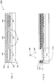
- FIG. 1 A non-limiting example of an OLED device 10 is shown in FIG. 1 and includes anode 11, hole-injecting layer (HIL) 12, hole-transporting layer (HTL) 13, electron-blocking layer (EBL) 14, light-emitting layer (LEL) 15 (sometimes referred to in the art as an emissive layer or EML), hole-blocking layer (HBL) 16, electron-transporting layer (ETL) 17, electron-injecting layer (EIL) 18 and cathode 19.
- the layers between the anode and cathode are often collectively referred to as the organic EL medium 20.
- OLED layer architectures known in the art having fewer or additional layers and there can be overlap in layer functionality.
- an EBL typically also has hole-transporting properties in addition to electron-blocking properties.
- An HBL if used, typically has electron-transporting properties.
- the LEL might have predominantly hole-transporting or electron-transporting properties, or it might have both.
- There can be multiple light emitting layers. So-called “tandem" architecture is known that includes one or more charge separation layers between light-emitting stacks that can double current efficiency.
- OLED materials useful for OLED devices are discussed below. Although the emphasis is on organic EL medium materials that can be vapor deposited, certain embodiments of the present disclosure may instead use solution deposited OLED materials. A few non-limiting examples of OLED material and structures can be found in US 8106582 and US 7955719 .
- the anode When EL emission is viewed through the anode, the anode should be substantially transparent to the emission of interest
- transparent herein means that at least 30% of emitted light is transmitted, preferably at least 50%.
- Common transparent anode materials used in the present disclosure are indium-tin oxide (ITO), indium-zinc oxide (IZO), and tin oxide, but other metal oxides can work including, but not limited to, aluminum- or indium-doped zinc oxide, magnesium-indium oxide, and nickel-tungsten oxide.
- metal nitrides such as gallium nitride, and metal selenides such as zinc selenide, and metal sulfides such as zinc sulfide, can be used as the anode.
- the transmissive characteristics of the anode are immaterial and many conductive materials can be used, regardless if transparent, opaque, or reflective.
- Example conductors for the present disclosure include, but are not limited to, gold, iridium, molybdenum, palladium, and platinum. Unless unique HIL materials are used, typical anode materials have a work function of at least 4.0 eV.
- EL emission is viewed through the cathode, it must be transparent or nearly transparent.
- metals must be thin (preferably less than 25 nm) or one may use transparent conductive oxides (e.g. indium-tin oxide, indium-zinc oxide), or a combination of these materials.
- transparent conductive oxides e.g. indium-tin oxide, indium-zinc oxide
- Some non-limiting examples of optically transparent cathodes have been described in more detail in U.S. Pat. No. 5,776,623 .
- any conductive material known to be useful in OLED devices may be selected, including metals such as aluminum, molybdenum, gold, iridium, silver, magnesium, the above transparent conductive oxides, or combinations of these.
- Desirable materials promote electron injection at low voltage and have effective stability.
- Useful cathode materials often contain a low work function metal ( ⁇ 4.0 eV) or metal alloy.
- Cathode materials can be deposited, for example, by evaporation, sputtering, or chemical vapor deposition.
- the HIL can be formed of a single material or a mixture of materials.
- the hole-injecting layer may be divided into several layers having different composition.
- the hole-injecting material can serve to improve the film formation property of subsequent layers and to facilitate injection of holes into the hole-transporting layer.
- Suitable materials for use in the hole-injecting layer include, but are not limited to porphyrin and phthalocyanine compounds as described in U.S. Pat. No. 4,720,432 , thiophene-containing compounds, phosphazine compounds, and certain aromatic amine compounds.
- the HIL may include an inorganic compound such as a metal oxide (e.g., molybdenum oxide), metal nitride, metal carbide, a complex of a metal ion and organic ligands, and a complex of a transition metal ion and organic ligands.
- Suitable materials for use in the hole-injecting layer may include plasma-deposited fluorocarbon polymers (CFx) as described in U.S. Pat. No. 6,208,075 , certain hexaazatriphenylene derivatives as described in U.S. Pat No. 6,720,573 B2 (e.g. hexacyanohexaazatriphenylene) or tetracyanoquinone derivatives such as F4TCNQ.
- CFx plasma-deposited fluorocarbon polymers
- the hole-injecting layer can also be composed of two components: for example, an aromatic amine compound, doped with a strong oxidizing agent, such as dipyrazino[2,3-f:2',3'-h]quinoxalinehexacarbonitrile, F4TCNQ, or FeCl 3 .
- a strong oxidizing agent such as dipyrazino[2,3-f:2',3'-h]quinoxalinehexacarbonitrile, F4TCNQ, or FeCl 3 .
- the HTL can be formed of a single or a mixture of organic or inorganic materials and may be divided into several layers.
- the hole-transporting layer most commonly includes a tertiary aryl amine, e.g., a benzidine or a carbazole, but instead (or in addition) may comprise a thiophene, or other electron-rich material.
- EBL materials are generally selected from the same group as HTL materials and have an electron conduction band significantly higher in energy (more difficult to reduce) than the overlying LEL thereby creating a barrier to further electron transport.
- the LEL commonly includes a host material and a light-emitting dopant. Injected holes and electrons recombine in the LEL. Hosts include HTL materials, ETL materials, a mixture of HTL and ETL materials or ambipolar materials readily capable of transporting holes and electrons. Examples of common hosts for singlet emission include polycyclic aromatic compounds such as anthracene derivatives. Examples of common hosts for triplet emission include carbazole compounds and aromatic amines. A wide variety of light-emitting dopants are known and are used to provide the desired emission wavelength by harvesting excitons created from the electron/hole charge injection. Many common singlet emitting dopants are aromatic organic compounds whereas many common triplet emitting dopants are metal complexes of iridium or platinum.
- the ETL can be formed of a single or a mixture of organic or inorganic materials and may be divided into several layers.
- Common ETL materials include metal oxine chelates such as Alq, phenanthroline derivatives such as BCP, triazenes, benzimidazoles, triazoles, oxadiazoles, silane compounds such as silacyclopentadiene derivatives, and borane derivatives.
- HBL materials are generally selected from the same group as ETL materials and have hole conduction band significantly lower in energy (more difficult to oxidize) than the underlying LEL thereby creating a barrier to further hole transport.
- the EIL may include an ETL material plus a reducing dopant at or near the interface between the cathode and ETL.
- the reducing dopant can be organic, inorganic, or metal complexes. Common reducing dopants include alkali metals such as Cs or combinations of alkali metals.
- the EIL may include an alkali or alkaline metal complex, salt or oxide (e.g., lithium quinolate, LiF, CaO) that forms a reducing dopant upon deposition of a cathode material such as aluminum.
- organic EL medium materials onto a substrate
- a substrate including, but not limited to, solution coating, vapor deposition, and transfer from a donor sheet
- vapor deposition means e.g., physical vapor deposition in a reduced pressure environment.
- most or all of the organic EL medium layers are provided by vapor deposition.
- vapor deposition equipment Many types are suitable. Such equipment may use point sources, linear sources, vapor-injection sources, carrier gas-assisted sources (OVPD) and the like.
- OVPD carrier gas-assisted sources
- the vapor plume is preferably highly directional to achieve a controlled line-of-site deposition through a patterned photoresist structure as will be shown later.
- OLED device substrates may be rigid or flexible.
- Support materials include, but are not limited to, glass, polymers, ceramics and metals, and composites or laminates thereof.
- AMOLED backplanes typically include an array of independently addressable first (bottom) electrodes that are connected to thin film transistor (TFT) circuitry provided over a substrate typically in a multilayer structure.
- TFT thin film transistor
- the TFT may be based on Si, metal oxide or organic semiconductors (OTFT).
- OTFT organic semiconductors
- dielectrics and conductors are used to prepare structures that form the transistors, capacitors, wiring, etc. as is known in the art.
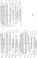
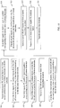
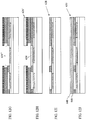
- FIG. 2 is a flow diagram showing steps for forming a three-color (e.g. RGB) active matrix OLED device according to an embodiment of the present invention.
- FIGS. 3A through 3K show portions of these steps in cross sectional form.
- a first lift-off structure e.g. an undercut lift-off structure
- the lift-off structure has an array of openings corresponding to a first array of bottom electrodes.
- the bottom electrodes may serve as anodes as part of a "standard structure” OLED or serve as cathodes as part of an "inverted structure” OLED.
- the bottom electrodes are already formed as part of the OLED substrate, but optionally, the bottom electrodes may be formed or further modified by depositing one or more desired anode or cathode materials through the array of openings of the lift-off structure (not shown in FIG. 2 ).
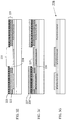
- FIG. 3A shows an embodiment of an OLED substrate 200 or backplane having a support 201 (e.g., flexible or non-flexible glass, plastic or ceramic), a TFT layer portion 202 (which may include multiple layers of wiring, dielectric and semiconductor materials), a first bottom electrode 210, a second bottom electrode 220, a third bottom electrode 230 and an electrode-separating dielectric 203.
- the first, second and third bottom electrodes each represent one bottom electrode in a first, second and third array of bottom electrodes, respectively, all independently addressable. That is, the first array of bottom electrodes forms a portion of a first array of independently addressable first OLED devices, the second array of bottom electrodes forms a portion of a second array of independently addressable second OLED devices and so on as needed.
- the electrode-separating dielectric often extends above and slightly over the edges of the bottom electrodes and may serve to help define the functional emissive area of the corresponding OLED device.
- the substrate may further include common organic EL medium layers that will make up a portion of each organic EL element.
- the substrate may include a common HTL and HTL.
- FIG. 3B shows a first lift-off structure 211 having an opening 215 corresponding to the first bottom electrode.
- the first lift-off structure 211 is a bilayer of first material layer 212 and first patterned photoresist layer 213.
- An undercut region 214 is formed in layer 212.
- the first lift-off structure 211 may instead be a single layer or have more than two layers. Lift-off structures are discussed in more detail later.
- step 103 includes cleaning residue from the first array of bottom electrodes (or from any optional common organic EL medium layers) using "dry etching” methods.
- dry etchant is used broadly and refers to any useful gaseous material possessing energy sufficient to clean a target area.
- Dry etching includes, but is not limited to, glow discharge methods (e.g., sputter etching and reactive ion etching), ion beam etching (e.g., ion milling, reactive ion beam etching, ion beam assisted chemical etching) and other "beam" methods (e.g., ECR etching and downstream etching), all of which are methods known in the art
- Some common dry etchants include oxygen plasma, argon plasma, UV/ozone, CF 4 and SF 6 , and various combinations.
- a substantially non-oxidizing plasma may be used, e.g., one including hydrogen and a non-oxidizing gas such as nitrogen or helium.
- the first organic EL medium layer(s) are deposited in step 105 followed by deposition of the first top electrode in step 107 over the first organic EL medium layers.
- a portion of the first organic EL medium layers 216' is deposited over the lift-off structure whereas another portion of the first organic EL medium layers 216 goes through the opening 215 and is deposited on the first array of bottom electrodes.
- a portion of the first top electrode 217' is deposited over the lift-off structure and onto organic EL medium layers 216' whereas another portion of the first top electrode 217 goes through opening 215 and is deposited onto first organic EL medium layers 216.
- the substrate included any optional common organic EL medium layers as discussed above, the first organic EL medium layers 216 would include those necessary to finish the OLED stack over the first array of bottom electrodes.
- step 109 the lift-off structure is removed along with the overlying first organic EL medium layers 216' and first top electrode 217'.
- this is done by providing a fluorinated solvent that dissolves the first material layer 212 but that is orthogonal to the patterned photoresist, organic EL medium materials and cathode.
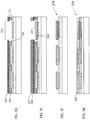
- This detaches the first patterned photoresist 213 and overlying layers 216' and 217', thereby forming a first intermediate structure 218 as shown in FIG. 3D having a first array of OLED devices, e.g., red-emitting OLEDs, each having a bottom electrode 210, organic EL medium layers 216 and top electrode 217.
- the lift-off solvent may swell the lift-off structure thereby causing its delamination or otherwise affect the adhesion between the substrate and the lift-off structure.
- Steps 101 through 109 are basically repeated two more times in steps 111 through 119 and steps 121 through 129, but with different sets of organic EL medium layers ( 226 and 236, FIGS. 3F and 3I ) to form second and third arrays of OLED devices, e.g., green and blue.
- a second lift-off structure is formed over the first intermediate structure.
- the second lift-off structure has an array of openings corresponding to a second array of bottom electrodes.
- FIG. 3E shows a second lift-off structure 221 having an opening 225 corresponding to the second bottom electrode.
- the second lift-off structure 221 is again a bilayer of second material layer 222 and second patterned photoresist layer 223.
- An undercut region 224 is formed in layer 222.
- the second lift-off structure 221 may instead be a single layer or have more than two layers.
- the materials and methods used to form second lift-off structure 221 may be the same as or different from those used to form the first lift-off structure 211.
- Step 113 in FIG. 2 indicates a step of cleaning residue from the second array of bottom electrodes using one of the methods previously described with respect to step 103.
- the residue cleaning method may the same as or different from step 103.
- the second organic EL medium layers are deposited in step 115 followed by deposition of the first top electrode in step 117 over the second organic EL medium layers.
- the second organic EL medium layers are different from the first organic EL medium layers, e.g., to provide a different emission color.
- the second top electrode may be the same as the first top electrode, but it may also be different, e.g., in order to achieve some desired charge injection or property.
- a portion of the second organic EL medium layers 226' is deposited over the lift-off structure whereas another portion of the second organic EL medium layers 226 goes through the opening 225 and is deposited on the second array of bottom electrodes.
- a portion of the second top electrode 227' is deposited over the lift-off structure and onto second organic EL medium layers 226' whereas another portion of the second top electrode 227 goes through opening 225 and is deposited onto second organic EL medium layers 226.
- step 119 the lift-off structure is removed along with the overlying second organic EL medium layers 226' and second top electrode 227', e.g., by providing a fluorinated solvent that dissolves the second material layer 222, in a manner analogous to that previously described for step 109.
- Removal of the second lift off structure fonns a second intermediate structure 228 as shown in FIG. 3G having a first array of OLED devices, e.g., red-emitting OLEDs, and a second array of OLED devices, e.g., green-emitting OLEDs, each having a bottom electrode 220, organic EL medium layers 226 and top electrode 227.
- a third lift-off structure is formed over the second intermediate structure.
- the third lift-off structure has an array of openings corresponding to a third array of bottom electrodes.
- FIG. 3H shows a third lift-off structure 231 having an opening 235 corresponding to the third bottom electrode.
- the first lift-off structure 231 is again a bilayer of third material layer 232 and third patterned photoresist layer 233.
- An undercut region 234 is formed in layer 232.
- the third lift-off structure 231 may instead be a single layer or have more than two layers.
- the materials and methods used to form third lift-off structure 231 may be the same as, or different from, those used to form the first or second lift-off structures.
- Step 123 in FIG. 2 indicates a step of cleaning residue from the third array of bottom electrodes using one of the methods previously described with respect to step 103.
- the residue cleaning method may the same as or different from step 103.
- the third organic EL medium layers are deposited in step 125 followed by deposition of the third top electrode in step 127 over the third organic EL medium layers.
- the third organic EL medium layers are different from the first and second organic EL medium layers, e.g., to provide a different emission color.
- the third top electrode may be the same as the first or second top electrode, but it may also be different, e.g., in order to achieve some desired charge injection or property.
- a portion of the third organic EL medium layers 236' is deposited over the lift-off structure whereas another portion of the third organic EL medium layers 236 goes through the opening 235 and is deposited on the third array of bottom electrodes.
- a portion of the third top electrode 237' is deposited over the lift-off structure and onto third organic EL medium layers 236' whereas another portion of the third top electrode 237 goes through opening 235 and is deposited onto third organic EL medium layers 236.
- step 129 the third lift-off structure is removed along with the overlying third organic EL medium layers 236' and third top electrode 237', e.g., by providing a solvent that dissolves the third material layer 232, in a manner analogous to that previously described for step 109.
- Removal of the third lift off structure forms a third intermediate structure 238 as shown in FIG. 3J having a first array of OLED devices, e.g., red-emitting OLEDs, and a second array of OLED devices, e.g., green-emitting OLEDs, and a third array of OLED devices, e.g., blue-emitting, each having a bottom electrode 230, organic EL medium layers 236 and top electrode 237.
- step 131 includes depositing a common top electrode 240 over the first, second and third arrays of OLED devices thereby electrically connecting the first, second and third top electrodes and forming active matrix OLED device 250.
- the material used for the common top electrode may be the same or different.
- the top electrodes Prior to depositing the common top electrode, the top electrodes may be treated to improve electrical contact with the common top electrode. This can help overcome contact resistance introduced by metal oxide or thin polymer residue that may be present on the top electrodes.
- the top electrodes may be treated with a low work function metal, e.g., an alkali metal, an alkaline metal or an alkaline earth metal.
- treatment may include a reducing gas environment, e.g. a gas environment including hydrogen.
- treatment may include a substantially non-oxidizing plasma, e.g. one including hydrogen and another non-oxidizing gas such as nitrogen or helium.
- treatment may include contact with a cleaning agent having a chemical composition different from the lift-off agent, the cleaning agent including a fluorinated solvent
- the cleaning agent may include a fluorinated solvent and a protic solvent such as an alcohol (e.g. IPA) at 15% or less by volume, alternatively 5% or less by volume.
- an alcohol e.g. IPA
- the protic solvent may include an organic acid at 5% or less by weight or alternatively 1 % or less by weight
- the cleaning agent may include a mixture of two fluorinated solvents, e.g., a mixture of a fluorinated solvent used in the lift-off agent and a second fluorinated solvent that is more polar or has less fluorine content by weight or both.
- the lift-off structure allows separation of "unwanted” overlying active materials (e.g., OLED materials) in the lift-off patterning process.
- active materials e.g., OLED materials
- at least a portion of the lift-off structure is soluble in a fluorinated solvent that is orthogonal to the array of OLED devices and the dissolution of this portion enables the separation.
- the lift-off structure has a substantially vertical sidewall profile (e.g., 90° ⁇ 10° relative to the substrate), or preferably, an undercut sidewall profile. The undercut reduces the amount of OLED material that deposits on the sidewalls so that the sidewalls remain unblocked to an appropriate lift-off agent.
- the thickness of the lift-off structure depends on the particular type of device and intended dimensions, but in general, it is in a range of 0.1 to 10 ⁇ m, alternatively in a range of 0.2 to 5 ⁇ m, or alternatively in a range of 0.5 to 3 ⁇ m.
- the lift-off structure includes a layer of a fluorinated material in contact with one or more underlying OLED device layers.
- the fluorinated material is photosensitive and can form the lift-off structure by exposure to radiation and development. Such a material may be a positive working (portions exposed to radiation are removed during development) or negative working (portions not exposed to radiation are removed during development).
- photosensitive fluorinated materials and systems include those disclosed in US Patent Application Nos.
- the photosensitive fluorinated material is a negative working photopolymer provided from a fluorinated solvent, e.g., a hydrofluoroether.
- the photosensitive fluorinated photopolymer is developed in a developing agent comprising one or more fluorinated solvents, e.g., a hydrofluoroether.
- a lift-off agent for use with a photosensitive fluorinated photopolymer includes a fluorinated solvent, e.g., a hydrofluoroether. The action of the lift-off agent is to dissolve the photopatterned fluoropolymer or alternatively cause delamination of the photopatterned polymer to the substrate, e.g., by swelling or inducing adhesion failure.
- the lift-off structure includes multiple layers, e.g., as shown in FIG. 3 and as described in US Patent Application No. 12/864,407 .
- a material layer comprising a fluorinated material such as a fluorinated molecular solid or fluorinated polymer is provided over a device substrate that may include an active organic material.
- the fluorinated material may be vapor deposited (e.g., if a molecular solid) or coated from a highly fluorinated solvent including, but not limited to, a hydrofluoroether or a perfluorinated solvent
- This layer forms the base of the multi-layer lift-off structure and is designed to be chemically inert relative to the underlying device substrate. It does not require photo-active elements such as photoacid generators or reactive groups that may, in some cases, harm the underlying device.
- the base layer may optionally comprise a light absorbing material to protect the underlying device from potentially high-intensity radiation of the overlying photoresist layer (see below).
- the light absorbing material is preferably incorporated into base the layer covalently, e.g., by attaching a light absorbing dye to a fluorinated polymer.
- the base layer is further designed to be readily soluble in a fluorinated or other orthogonal solvent to enable rapid lift-off as described earlier.
- the lift-off agent may cause delamination of the base layer from the substrate, e.g., by swelling or inducing adhesion failure.
- a photoresist layer is applied, e.g., from a coating solvent or by lamination.
- the photoresist can be a conventional photoresist (positive or negative tone) coated from, or processed with, solvents that would normally be harmful to the underlying device substrate, but the base layer blocks penetration of such harmful materials.
- the photoresist transforms in some way to alter its solubility relative to unexposed photoresist For example, exposure may activate solubility-altering switching groups, induce cross-linking or cause chain scission.
- the photoresist may optionally be a fluorinated photoresist provided from a fluorinated coating solvent so long as the underlying base layer retains at least some of its structural integrity, i.e., it is not dissolved too quickly by the coating solvent.
- fluorinated photoresists may be generally benign, an additional layer of separation from the photoactive layer of photoresist can in some embodiments provide extra protection.
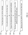
- FIG. 4 A flow diagram for an embodiment of forming a two-layer lift-off structure is shown in FIG. 4 , and in cross-sectional view in FIG. 5 .
- Such lift-off structures may be used in the embodiments described in FIGS. 2 and 3 .
- a base layer 311 is formed over device substrate 310.
- the base layer may undergo subsequent processing steps such as curing, drying, surface treatments or the like.
- a photoresist layer 312 is formed over base layer 311.
- the photoresist layer may undergo drying or other steps prior to step 305 wherein the photoresist layer 312 is exposed to patterned radiation by providing a radiation source 313 and an intervening photomask 314.
- the photoresist is a negative tone type, but a positive tone could be used instead.
- Other methods of photopatterning may optionally be used, e.g., projection exposure, patterned laser exposure and the like.
- the exposed photoresist layer is developed with a developing agent (e.g., an aqueous, alkaline developer if using many conventional photoresists), which in this embodiment, removes unexposed photoresist regions 316 to form a first pattern of uncovered base layer 318.
- a developing agent e.g., an aqueous, alkaline developer if using many conventional photoresists
- the first pattern of uncovered base layer is removed, for example, by using a fluorinated developing agent such as a hydrofluoroether to form lift-off structure 319 having a first pattern of openings 320.
- the removal of the base layer forms an undercut region 321.
- the structure is subjected to a lift-off agent that dissolves the base layer.
- a lift-off agent that dissolves the base layer.
- the lift-off agent may be a fluorinated solvent, including but not limited to, hydrofluoroethers and perfluorinated solvents.
- a fluorinated photoresist or a fluorinated base layer may be coated or processed (e.g., development or lift-off) using a fluorinated solvent.
- fluorinated solvents include those that are perfluorinated or highly fluorinated liquids at room temperature, which are immiscible with water and many organic solvents.
- hydrofluoroethers HFEs
- HFEs including segregated HFEs, are preferred solvents because they are non-flammable, have zero ozone-depletion potential, lower global warming potential than PFCs and show very low toxicity to humans.
- HFEs and isomeric mixtures of HFEs include, but are not limited to, an isomeric mixture of methyl nonafluorobutyl ether and methyl nonafluoroisobutyl ether (HFE-7100), an isomeric mixture of ethyl nonafluorobutyl ether and ethyl nonafluoroisobutyl ether (HFE-7200 aka NovecTM 7200), 3-ethoxy-1, 1,1,2,3,4,4,5,5,6,6,6-dodecafluoro-2-trifluoromethyl-hexane (HFE-7500 aka NovecTM 7500), 1,1,1,2,3,3-hexafluoro-4-(1,1,2,3,3,3,-hexafluoropropoxy)-pentane (HFE-7600 aka PF7600 (from 3M)), 1-methoxyheptafluoropropane (HFE-7000), 1,1,1,2,2,3,4,5,5,5-decafluoro
- the lift-off structure absorbs or blocks underlying layers from at least 80% of any imaging radiation used in the formation of the lift-off structure.
- the photoresist portion of the lift-off structure is formed using a positive-type of photoresist. In this way, any underlying OLED devices or structures will not be exposed to potentially harmful imaging radiation.
- steps 105, 115, and 115 may be done under a low pressure (vacuum) environment that has low oxygen and water.
- the substrate will likely be removed from the low pressure environment into an ambient environment for other steps relating to removal (lift-off) of lift-off structures and forming additional lift-off structures.
- each OLED stack is provided up through at least its respective LEL, but does not include an EIL or any layers having electron rich dopants such as alkali metal, alkaline metal or alkaline earth metal dopants.
- the OLED stack may be provided up to and including the HBL.
- a common cathode layer and optional common organic EL medium layers such as EIL or ETL or both) can be applied at the end of the process and such common EIL/cathode layers will not be exposed to potential water and oxygen contamination that may arise in the lift-off related processes.
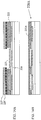
- FIG. 6 This alternative process flow is shown in FIG. 6 and is in other respects the same as shown in FIG. 2 .
- steps 401 through 431 correspond to steps 101 through 131 of FIG. 2 , respectively.
- the differences in FIG. 6 are: 1) the bottom electrodes are now referred to as bottom anodes; 2) the steps of depositing first, second and third top electrodes are absent; and 3) a new step 430 is introduced which has no counterpart in FIG. 2 whereby one or more common organic EL media layers are optionally deposited over the third intermediate structure.
- FIG. 7 a cross-sectional view of an active matrix OLED 450 made in an embodiment according to FIG. 6 is shown in FIG. 7 , which is analogous to FIG. 3J .
- reference numbers 201, 202, 203, 210, 220, and 230 are as described above for FIG. 3 .
- the first, second and third organic EL medium layers, 440, 442, and 444 include only layers other than an EIL.
- An optional common EIL layer 446 is provided over the organic medium layers and a common cathode 448 is provided over the common EIL layer.
- the substrate may have included common HIL and HTL layers as described previously. Prior to depositing the common top electrode, or alternatively, a common organic EL layer if that is included, the top surface of the patterned organic EL medium layers may be treated to improve contact with the common top electrode or common organic EL layer.
- the top surface of the organic EL medium layers may be treated with a low work function metal, e.g., an alkali metal, an alkaline metal or an alkaline earth metal.
- a low work function metal e.g., an alkali metal, an alkaline metal or an alkaline earth metal.
- the low work function metal has a thickness of less 2 nm or less, alternatively 1 nm or less, or even 0.5 nm or less.
- treatment may include a reducing gas environment, e.g. a gas environment including hydrogen.
- treatment may include a substantially non-oxidizing plasma, e.g. one including hydrogen and another non-oxidizing gas such as nitrogen or helium.
- treatment may include contact with a cleaning agent having a chemical composition different from the lift-off agent, the cleaning agent including a fluorinated solvent.
- the cleaning agent may include a fluorinated solvent and a protic solvent such as an alcohol (e.g. IPA) at 15% or less by volume, alternatively 5% or less by volume.
- the protic solvent may include an organic acid at 5% or less by weight or alternatively 1 % or less by weight
- the cleaning agent may include a mixture of two fluorinated solvents, e.g., a mixture of a fluorinated solvent used in the lift-off agent and a second fluorinated solvent that is more polar or has less fluorine content by weight or both.
- the top electrodes 217, 227 and 237 are provided in a manner so that they cover a slightly larger area than the organic EL medium layers. This can be done by reducing the collimation of the top electrode deposition e.g., by moving the top electrode source closer to the substrate as shown in FIG. 8 . This allows the top electrode material to extend beyond the edges of the OLED and help seal the exposed edges to protect from water and oxygen penetration.
- top electrode source 480 is positioned so that top electrode material 482 emitted from the source is not highly collimated and deposits a first top electrode 217 that, in this embodiment, includes top electrode portion 217a that extends over the sides of organic EL medium layers 216.
- a top electrode material should be of a material and thickness so that it is relatively inert itself to water and oxygen penetration, or able to form a non-harmful, inert oxide barrier layer.
- the top electrode may comprise aluminum or metal oxide that is at least 50 nm, preferably at least 100 nm thick.
- the top electrode in this embodiment may be a cathode or anode.
- the organic EL medium layers should be deposited in an area at least as large as the bottom electrode, preferably larger, and it is preferred that the substrate include a bottom electrode-defining dielectric. This will prevent shorting of the two electrodes.
- the top layer of the organic EL media layers can be provided to cover the edges of underlying organic EL media layers.
- the top organic EL media layer of an individual stack is a hole-blocking layer that is provided in an area slightly larger than the underlying layers, e.g., to protect edges of the LEL or other layers which may be more water or oxygen sensitive than the HBL. This can also be done by selecting conditions for top organic EL media layer deposition that are less collimated than underlying layers.
- the OLED arrays each have an inverted structure wherein the cathode is the bottom electrode and the anode is the top electrode.
- the top anode may further be provided to cover the edges of the organic EL medium as described in FIG. 8 .
- the sensitive EIL and cathode/EIL are at the bottom and further away from the lift-off structure, its associated chemistry and potential adventitious water and oxygen thereby providing a more robust structure.
- a fluorinated material layer is vapor deposited after deposition of the first or second top electrodes or both, i.e., after step 107, but before step 109, or after step 117, but before step 119.
- the organic EL medium and top electrodes are deposited in a reduced pressure (vacuum) environment as discussed previously.
- the vapor deposited fluorinated material layer can serve as a temporary barrier to water, or as a buffer layer against physical damage from handling, when the substrate is transferred to more ambient pressure conditions for lift-off processing.
- An example structure is shown in cross sectional view in FIG. 9 which is identical to FIG.
- the fluorinated material layer is chosen to dissolve in the lift-off solvent
- the fluorinated material layer is selected so that it does not dissolve in the lift off solvent, but rather, remains over the active OLED device and is lifted off in the photoresist portions along with the unnecessary OLED and top electrode materials as described earlier. Prior to deposition of the common top electrode, however, the fluorinated material layer should be removed in an orthogonal solvent other than the lift-off solvent from steps 109 and 119.
- the lift off solvent may be a first hydrofluoroether and the fluorinated material layer removal step may use a different hydrofluoroether or a perfluorinated solvent, or vice versa and the lift-off solvent is a perfluorinated solvent.
- vapor deposited fluorinated material layer may be provided after deposition of the organic EL medium layers, e.g., after step 405 but before step 409.
- the fluorinated material layer may be chosen to dissolve in the lift-off solvent, or alternatively, the fluorinated material layer is selected so that it does not dissolve in the lift off solvent. If the latter, prior to deposition of the common top electrode and any common organic layers, the fluorinated material layer should be removed in an orthogonal solvent other than the lift-off solvent from steps 109 and 119.
- one or more of the lift-off structures has a multi-layer structure, e.g., the two-layer structure shown in FIG. 3 and further illustrated in FIG. 5 .
- the lift-off structure is removed by using lift-off agent comprising a fluorinated solvent having a density greater than the effective density of the photoresist layer plus overlying organic EL medium layers and the cathode.
- "effective density” is the total mass of the photoresist layer plus any overlying layers divided by the volume of such photoresist layer and overlying layers.
- the photoresist or cathode is selected to have some residual stress that encourages the lift-off portion to curl during lift off. This curling action can more quickly expose fresh base layer thereby speeding up the lift-off step.
- the curl force induces an arc of at least 180° in at least a portion of the lift-off structure. In an embodiment, the curl force induces an arc of at least 360° in at least a portion of the lift-off structure, i.e., at least a portion of the lift-off structure rolls up on itself.
- the cathode is selected to have some magnetic properties so that a magnet in a lift-off agent bath can attract the removed portion. This can speed up lift off and also reduce the chance that possible debris from the lift-off materials will damage the remaining OLED structure.
- the common top electrode deposition might not go as drawn. If the common top electrode is thinner than the organic EL thickness, there is chance for a discontinuity as shown in FIG. 10A , which is otherwise the same as FIG. 3K except that the thin common top electrode 241 does not readily connect the other top electrodes. This may produce a defective active matrix OLED device, 251. Further, even as drawn in FIG. 3K , there is a chance for shorting between the top and bottom electrodes.
- a patterned dielectric layer is provided after forming the third intermediate structure to aid the deposition of the common top electrode.
- Such patterned dielectric may be provided from a fluorinated photopolymer from a fluorinated solvent, e.g., a cross-linking fluorinated polymer as described in International Application Nos. PCT/US2014/047800 and PCT/US2015/014425 , exposing and developing in an orthogonal developing agent.
- the patterned (optionally fluorinated) dielectric 495 is provided over third intermediate structure 238 that is otherwise the same as that shown in FIG. 3J .
- the patterned dielectric 495 has a relatively gentle slope to ensure good contact between the top electrodes of each OLED array and the common top electrode 242, even if the common top electrode is thinner than the organic EL medium thickness. Further, there is now considerable separation between the top electrode and bottom electrodes, reducing the chance for shorts.
- the array of patterned openings in the dielectric (sometimes referred to as a "pixel definition layer" or PDL) generally defines the display region of a display device.
- the lift-off structures employ a negative type photoresist and the top electrodes are substantially opaque to patterning radiation. In this way, underlying organic EL media layers are protected from potentially harmful radiation such as UV light.
- three lift-off structures are fabricated to pattern three different colors.
- only two lift-off structures are used as described in FIGS. 11 and 12A-12J .
- step 501 third organic EL medium layers (e.g. for a red-emitting OLED) are deposited over an OLED substrate having first, second and third arrays of bottom electrodes.
- the third organic EL medium layers will eventually be used to form an OLED over the third array of bottom electrode.
- FIG. 12A This is shown in cross-sectional view in FIG. 12A wherein an OLED substrate (having first, second and third arrays of bottom electrodes) is provided as described previously in FIG. 3A and the third organic EL medium layers 636 are commonly deposited over all of the arrays of electrodes. A top electrode is not provided at this time.
- the third organic EL medium is easily dry-etched and does not include substantial amounts of metal-containing materials in its LEL, optional HBL or optional ETL, e.g., aluminum quinolate complexes or phosphorescent iridium dopants.
- a first lift-off structure is formed having an array of openings corresponding to a first array of bottom electrodes.
- FIG. 12B shows a first lift-off structure 611 having an opening 615 corresponding to a first bottom electrode.
- the first lift-off structure 611 is a bilayer of first material layer 612 and first patterned photoresist layer 613.
- An undercut region 614 is formed in layer 612.
- the first lift-off structure 611 may instead be a single layer or have more than two layers.
- the first-lift off structure is used as an etch mask for etching the third organic EL medium layers. These layers are etched in a pattern corresponding to the first array of bottom electrodes. As shown in FIG. 12C , the removed portion 636' of the third organic EL medium layers exposes the first array of bottom electrodes for subsequent OLED deposition steps as described below. Methods of etching include those mentioned above with respect to dry-etching. In an embodiment, the electrode-separating dielectric 203 (see FIG. 3A ) is more etch resistant than the organic EL medium layers.
- first organic EL medium layers (e.g., for a green-emitting OLED) are deposited. As shown in FIG. 12D , a portion of the first organic EL medium layers 616' is deposited over the lift-off structure whereas another portion of the first organic EL medium layers 616 goes through the opening 615 and is deposited on the first array of bottom electrodes. Although not shown in the present embodiment, a first top electrode may optionally be deposited over the first organic EL medium layers in a manner similar to that shown in FIG. 3C .
- the first lift-off structure is removed to form a first intermediate structure 618 as shown in FIG. 12E .
- a second lift-off structure 621 having an array of openings 625 corresponding to the second array of bottom electrodes is formed over the first intermediate structure.
- the second lift-off structure 621 is a bilayer of second material layer 622 and second patterned photoresist layer 623.
- An undercut region 624 is formed in layer 622.
- the second lift-off structure 621 may instead be a single layer or have more than two layers.
- the second-lift off structure is used as an etch mask for etching the first organic EL medium layers. These layers are etched in a pattern corresponding to the second array of bottom electrodes. As shown in FIG. 12G , the removed portion 636" of the first organic EL medium layers exposes the first array of bottom electrodes for subsequent OLED deposition steps as described below. Methods of etching include those mentioned above with respect to dry-etching. In an embodiment, the electrode-separating dielectric 203 (see FIG. 3A ) is more etch resistant than the organic EL medium layers.
- second organic EL medium layers are deposited. As shown in FIG. 12H , a portion of the second organic EL medium layers 626' is deposited over the lift-off structure whereas another portion of second third organic EL medium layers 626 goes through the opening 625 and is deposited on the second array of bottom electrodes. Although not shown in the present embodiment, a second top electrode may optionally be deposited over the second organic EL medium layers in a manner similar to that shown in FIG. 3C .
- step 517 the second lift-off structure is removed to form a second intermediate structure 628 as shown in FIG. 12I .
- steps 519 one or more common organic EL medium layers 646 are optionally provided over the second intermediate structure and in step 521 a common electrode 648 is provided thereby forming active matrix OLED device 650.
- FIG. 12J shows the embodiment with the optional common organic EL medium layer(s) 646.
- first and second top electrodes should not be deposited over the first and second organic EL medium layers.
- the top surfaces of patterned organic EL medium layers may optionally be cleaned or treated as previously described with respect to FIGS. 6 and 7 .
- each OLED stack is provided up through at least its respective LEL, but does not include an EIL or any layers having electron rich dopants such as alkali metal, alkaline metal or alkaline earth metal dopants.
- the OLED stack may be provided up to and including a hole-blocking layer.
- third organic EL medium layers may be provided in interstitial areas between the first and second organic EL medium layers. This can be advantageous for providing a uniform surface for the deposition of subsequent common layers. It also may help prevent shorts in the event that a device has a defect (e.g. in the PDL or in the patterning of other colors) that exposes an unintended area of a bottom electrode.
- the third organic EL medium layers would cover such defect, and although it may slightly reduce the color purity of a defective pixel if it was intended to emit colors from the first or second organic EL medium layers, it would more importantly light up upon application of an appropriate voltage rather than producing a dark spot.
- one or more of the third organic EL medium layers are coated from solution.
- one or more of the third and first organic EL medium layers are coated from solution.
- the third organic EL medium includes a light-emitting layer deposited from solution (e.g., a polymeric LEL) whereas the first organic EL medium or second organic EL medium or both includes an LEL provided by vapor deposition.
- FIGS. 11 and 12 An advantage of the embodiments shown in FIGS. 11 and 12 is that only two lift-off steps are required for a three-color OLED.
- FIGS. 13A through 13D shows a series of cross-sectional views in another embodiment of forming an organic device.
- a device substrate 700 is provided, which may optionally be flexible and may optionally include a support layer (e.g. as described above for OLEDs) in addition to other layers and features necessary to provide a desired organic device.
- the organic device may be an OLED, a display, a lighting device, a chemical sensor, a touch sensor, a photovoltaic, a TFT backplane, or a bioelectronic or medical device.
- first undercut lift-off structure 711 having a first opening 715 and forms an area of uncovered device substrate 703.
- the lift-off structure may include any of those previously discussed so long as there is an undercut.
- the first undercut lift-off structure 711 is a single layer having undercut region 714, e.g., a patterned fluorinated photoresist developed using a fluorinated solvent
- the undercut lift-off structure could instead comprise two or more patterned layers, e.g., including a fluorinated material base layer and an overlying photoresist layer wherein the fluorinated material base layer is undercut relative to the photoresist layer.
- a first active organic material layer is then deposited over the first undercut lift-off structure and over a first portion 705 of the area of uncovered device substrate.
- the active organic material deposited over the lift-off structure is shown as 713' and the active organic material deposited over the first portion is shown as 713.
- the first active organic material layer is vapor-deposited in a reduced-pressure environment with a reasonable amount of collimation so that the material is deposited in an area similar in size to opening 715.
- a growth catalyst, an adhesion promoter or a linking group is provided over the first portion 705 by a collimated means and the first active organic material layer is selectively deposited from solution or other non-collimated vapor phase in the areas occupied by the growth catalyst, adhesion promoter or linking group.
- the first active organic material layer may include, for example, an organic conductor, an organic semiconductor, a charge transport material, a light-emitting material, or a biological material.
- the first active organic material layer is sensitive to water or oxygen or both.
- a second material layer is deposited over the first active organic material layer and over a second portion 707 of the area of uncovered substrate.
- the second material layer deposited over the lift-off structure is shown as 717' and the second material layer deposited over the second portion is shown as 717.
- the second portion area is larger than the first portion area and so the second material layer 717 extends beyond and covers the sidewalls of the first active organic material layer 713 in the first portion.
- the second material layer may be deposited from solution or by vapor deposition so long as the vapor is not so highly collimated that it limits the second portion area to the degree that it prevents or limits coverage of the second material layer over the sidewalls of the first active organic material layer.
- a growth catalyst, an adhesion promoter or a linking group is provided over regions other than the sidewalls of the lift-off structure, and the second material layer is then selectively deposited from solution or other vapor phase in the areas occupied by the growth catalyst, adhesion promoter or linking group.
- the second material layer is electrically conductive.
- the second material layer may include an organic conductor, a metal, a metal oxide, graphene or graphene-oxide.
- the second material layer comprises a second active organic material different from the first active organic material layer.
- this second active organic material may include an upper layer in an organic EL media stack such as a charge transport material or light emitting material, or it may include a biological material or an organic semiconductor.
- the second material layer is later removed and does not form part of the organic device in its final form.
- the second material layer may include a fluorinated material.
- the second material layer is less sensitive to water or oxygen, or both, than the first active organic material layer.
- the second material layer at least partially protects the first active organic material layer from water or oxygen or both, for example, by slowing the ingress of water or oxygen.
- the first undercut lift-off structure is removed by treatment with a first lift-off agent comprising a fluorinated solvent, thereby forming an intermediate structure or organic device 720 having a patterned first active organic material layer and a patterned second material layer over the substrate.
- the first opening may optionally be part of a first array of openings having a first pattern.
- the substrate may optionally include a first array of bottom electrodes in alignment with the first openings.
- a lift-off structure may include a fluorinated material base layer and a photoresist wherein the fluorinated material base layer acts as a lift-off layer.
- the lift-off agent comprises a fluorinated solvent, e.g., a perfluorinated solvent or a hydrofluoroether, and a film-forming, lift-off fluorinated material that may be the same as or different from the fluorinated material used in the fluorinated material base layer.
- a fluorinated solvent e.g., a perfluorinated solvent or a hydrofluoroether
- a film-forming, lift-off fluorinated material that may be the same as or different from the fluorinated material used in the fluorinated material base layer.
- an intermediate device structure may be formed from the lift-off step and the intermediate structure is intended for further processing.
- a protective layer of the lift-off fluorinated material is formed upon evaporation or drying. This can protect underlying sensitive structures from adventitious contaminants and physical damage that may occur during storage or transfer to other processing stations.
- the lift-off fluorinated material is the same as the fluorinated material of the fluorinated material base layer and at least a portion of the lift-off fluorinated material in the lift-off agent is a seasoning byproduct of the lift-off step that is deliberately allowed to build up.
- a layer of such lift-off fluorinated material is deliberately allowed to form on a patterned device structure surface.
- the dried lift-off fluorinated material has a thickness in a range of 10 nm to 1000 nm thick, alternatively 50 nm to 500 nm.
- the layer of lift-off fluorinated material is thick enough to be used as a subsequent base layer in the fabrication of another lift-off structure for further patterning. In an embodiment, the layer of lift-off fluorinated material is largely dissolved into a subsequent fluorinated material base layer coating and becomes part of the new fluorinated material base layer.
- FIG. 14A shown in FIG. 14A is a structure identical to that described for FIG. 3F , and in particular, the second material layer 222 is a fluorinated material.
- the intermediate structure 228A of FIG. 14B is formed having a lift-off fluorinated material layer 222A. In an embodiment, this may be used to form a base layer, or a portion of a base layer, in another lift-off structure.
- the lift-off fluorinated material can be added to a lift-off process replenishment supply.
- the lift-off fluorinated material can be provided by seasoning a lift-off processing tank that allows build-up of a fluorinated material from the lift-off structure, preferably in conjunction with a replenishment system and a recirculation system for filtering insoluble lift-off portions.
- seasoning a lift-off processing tank that allows build-up of a fluorinated material from the lift-off structure, preferably in conjunction with a replenishment system and a recirculation system for filtering insoluble lift-off portions.
- it can save money by reducing the volume of fresh lift-off agent consumed.
- the intermediate structure should be cleaned with fresh lift-off agent or treated in ways previously described to remove residue prior to deposition of any common organic EL layers or a common top electrode.
- a glass substrate 800 was provided having three regions of conductive ITO as shown in FIG. 15A including center region 801 and two edge regions 802 and 802', each separated by stripes of non-conductive glass.
- a patterned dielectric 803 was formed over a portion of center ITO from positive photoresist (AZ1512, diluted) by conventional methods and hard-baked at 150 °C for 5 minutes.
- An expanded view of the patterned dielectric 803' shows that the pattern included an array of vertical rows of 804G, 804R, and 804B openings for subsequently deposited green, red and blue OLED layers.
- the patterned dielectric was about 500 nm thick and had highly tapered features as depicted in FIG.
- each pixel opening was 10 ⁇ m wide and 36 ⁇ m long, each separated by 4 ⁇ m in the horizontal direction (between colors) and 6 ⁇ m in the vertical direction (between same color pixels).
- each set of RGB pixels is 40 ⁇ m x 40 ⁇ m, which corresponds to a 635 dpi resolution color display with an emissive fill factor (aperture ratio) of 61%.
- Patterning of green, red and blue OLED pixels was carried out in a manner similar to that described with respect to FIGS. 2 and 3 . Rather than individually addressable bottom electrodes, however, a common anode (ITO) was provided as bottom electrode for all colors.
- Each lift-off structure was formed using a fluorinated material base layer and an overlying photoresist layer.
- the fluorinated material base layer was formed by coating a composition including a hydrofluoroether solvent with about 12% by weight of a methacrylate-based fluoropolymer having fluorine-containing pendant alkyl groups and non-fluorine containing pendant alkyl groups. The fluorine content of the fluoropolymer was about 49% by weight.
- the composition was spin coated over the substrate at 3000 rpm for 1 min and baked at 90 °C for 1 min on a hot plate. Thickness of the fluorinated material base layer was about 800 nm. This fluorinated material base layer had a planarizing effect over the patterned dielectric. In order to avoid difficulties in lift off, it was found that the thickness of fluorinated material base layer as measured from the ITO should be thicker than the height of the patterned dielectric, preferably at least 100 nm thicker.
- a conventional negative photoresist nLOF 2020 was applied by spin coating at 3500 rpm and baked at 110 °C for 1 min on a hot plate.
- the thickness of the photoresist was about 1.7 ⁇ m.
- the photoresist was then exposed on a Karl Suss contact aligner (365 nm) using a mask aligned with green pixels, the mask pixel features (openings) being about 1 ⁇ m larger in each dimension than the patterned dielectric openings.
- the exposure dose was 60 mJ/cm 2 and the structure was given a post exposure bake at 110 °C for 1 min on a hot plate.
- the nLOF was developed in CD-26 for 100-120 seconds, rinsed in DI water and blown dry with compressed air.
- the fluorinated material base layer was developed using two 30 sec "puddles" of HFE-7300 with spin drying after each 30 sec. A brief spray of HFE-7300 was also applied at the beginning of the spin dry to better remove the fluoropolymer from the pixel area.
- the structure was then subjected to a mild oxygen plasma etch (50 seem O 2 , 100 mT pressure, 100 W, 30 sec) to remove trace fluorinated material residue in the pixel wells.
- a mild oxygen plasma etch 50 seem O 2 , 100 mT pressure, 100 W, 30 sec
- the substrate with its lift-off structure was moved into an OLED deposition chamber and a green-emitting organic EL element was provided including vapor deposition of (in order) 10 nm HAT-CN, 80 nm NBP, 50 nm Alq, 0.5 nm LiF and 50 nm Al.
- the device was then moved into a nitrogen glove box and immersed in warm HFE7300 (between 50 °C and 60 °C) for a few minutes to dissolve the fluorinated material base layer.
- Lift off of the pixel patterned area occurred in less than 1 minute without agitation, although a large alignment mark area (not shown in FIG. 15 ) necessitated about 5 minutes with a small amount of agitation to remove the full structure.
- the photoresist portion with overlying OLED rolled up on itself thereby containing and reducing debris in solution.
- the lifted-off portion also tended to float to the surface of the lift-off bath due to its lower density making it relatively easy to remove.
- a pattern of OLEDs for green emission remained in the pixel areas corresponding to 804G in FIG. 15B .
- the sample patterned with the green OLED pixels was removed from the lift-off bath, rinsed with HFE7300 and then coated with a new fluorinated base layer in nitrogen glove box.
- the sample was removed into the ambient, nLOF 2020 was applied and the subsequent steps were similar to those described above, but in this case, to form a red-emitting organic EL element in the pixel areas in a manner similar to described above, but now for the red pixels (corresponding to 804R in FIG. 15B ).
- the red-emitting organic EL element included: 10 nm HAT-CN, 60 nm NBP, 40 nm of a 90:10 (by weight) mixture of NPB:Ir(MDQ) 2 (acac), 20 nm Alq, 0.5 nm LiF and 50 nm Al.
- the process was repeated again as previously described, but this time for the blue pixels corresponding to 804B in FIG. 15B .
- the blue-emitting organic EL element included 10 nm HAT-CN, 60 nm NPB, 40 nm of a 95:5 (by weight) mixture of ⁇ -ADN and DPAVBi, 20 nm Alq and 0.5 nm LiF. In this case, no aluminum was provided.
- the structure was treated in lift-off bath as previously described, rinsed with HFE-7300 and returned to OLED deposition chamber and a common aluminum cathode 805 was deposited over all of the OLED pixels as shown in FIG. 15C .
- the common cathode made contact with the end ITO stripes 802 and 802' so that they could be used as contacts.
- the OLED device was encapsulated in a metal can. No attempt was made to balance the voltage between the OLED structures and not all of the pixels turned on at the same time as voltage was applied to the structure, but all three pixels arrays lit up brightly at 12V thus showing that a full-color OLED device can be fabricated having resolution of > 630 dpi and an emissive fill factor (aperture ratio) of >60% with a spacing of only 4 ⁇ m between red, green and blue pixels.
- Example 2 This example was similar to Example 1, but with some notable changes.
- the processing sequence for Example 2 was similar to that shown in FIGS. 6 and 7 .
- the fluorinated material base layer was 900 nm Cytop 109A coated from a hydrofluoroether solvent and the photoresist was a negative tone, branched photosensitive fluoropolymer coated 1.2 ⁇ m from an HFE solvent similar to those described in US Application No. 14/539,574 .
- the fluoropolymer included fluorine-containing alkyl groups, acid-catalyzed, carboxylic acid forming precursor groups, sensitizing dye units, acid quenching units and had a fluorine content of about 40% by weight
- the coating composition further included a photoacid generating compound CGI-1907 at 1% by weight relative to the fluoropolymer.
- the photosensitive fluoropolymer has high solubility in HFE-7600. The authors have surprisingly found that Cytop has low solubility in HFE-7600, thereby enabling easy coating of the photosensitive fluoropolymer over the Cytop.
- the photosensitive fluoropolymer was exposed at 14 mJ/cm 2 (post apply and post exposure bakes done for 1 min at 90 °C) and was developed with a few second puddle of HFE-7100 which rapidly dissolves unexposed areas but not underlying Cytop.
- the underlying Cytop development and other lift-off structure processing steps were similar to those described previously.
- lift-off was occurring, the fluorinated photopolymer portion with overlying OLED rolled up on itself thereby containing and reducing debris in solution.
- the lifted-off portion also tended to float to the surface of the lift-off bath due to its lower density making it relatively easy to remove.
- the first pixel included (in order) 10 nm HAT-CN, 60 nm NBP, and 40 nm of a 90:10 (by weight) mixture of NPB:Ir(MDQ) 2 (acac).
- the second pixel included 10 nm HAT-CN and 80 nm of NPB.
- the third pixel included 10 nm HAT-CN, 60 nm NPB, 40 nm of a 95:5 (by weight) mixture of ⁇ -ADN and DPAVBi.
- a common layer of 30 nm Alq electron tranpsort layer was deposited over all of the pixels followed by a common layer of 0.5 nm LiF and 100 nm Al.
- the common Alq layer produced a green-emitting EL element.
- Example 2 had additional advantages that the turn on voltages were substantially reduced, fewer defects were observed and less shorting occured.
- the present disclosure enables a broad set of active organic materials to be photolithographically patterned to fine dimensions. Because special "photoresist compatible" OLED materials do not need to be selected, the user is free to use the best OLED materials to create the most effective structures possible for red, green and blue emission.
Claims (13)
- Procédé de fabrication d'un dispositif OLED comprenant :a) la fourniture d'un substrat de dispositif (201) présentant un premier réseau d'électrodes inférieures (210) et un deuxième réseau d'électrodes inférieures (220) ;b) la fourniture d'une première structure de décollement de contre-dépouille (211) par-dessus le substrat de dispositif (201) présentant un premier motif d'ouvertures (215) correspondant au premier réseau d'électrodes inférieures (210) ;c) le dépôt d'une ou plusieurs premières couches centrales EL organiques (216, 216') comportant au moins une première couche électroluminescente par-dessus la première structure de décollement de contre-dépouille (211) et par-dessus le premier réseau d'électrodes inférieures (210) ;d) le retrait de la première structure de décollement de contre-dépouille (211) et le recouvrement d'une(de) première(s) couche(s) centrale(s) EL organique(s) (216') par traitement avec un premier agent de décollement comprenant un solvant fluoré pour former une première structure intermédiaire (218) ;e) la fourniture d'une deuxième structure de décollement de contre-dépouille (221) par-dessus la première structure intermédiaire (218) présentant un deuxième motif d'ouvertures (225) correspondant au deuxième réseau d'électrodes inférieures (220) ;f) le dépôt d'une ou plusieurs deuxièmes couches centrales EL organiques (226, 226') comportant au moins une deuxième couche électroluminescente par-dessus la deuxième structure de décollement de contre-dépouille (221) et par-dessus le deuxième réseau d'électrodes inférieures (220) ;g) le retrait de la deuxième structure de décollement de contre-dépouille (221) et le recouvrement d'une(de) deuxième(s) couche(s) centrale(s) EL organique(s) (226') par traitement avec un deuxième agent de décollement comprenant un solvant fluoré pour former une deuxième structure intermédiaire (228) ; eth) la fourniture d'une électrode supérieure commune (241, 242) en contact électrique avec les premières et deuxièmes couches centrales EL organiques (216, 226) ;
le procédé étant caractérisé en ce qu'au moins une structure de décollement (211, 221) absorbe ou bloque des couches sous-jacentes vis-à-vis d'au moins 80 % de rayonnement d'imagerie utilisé lors de la formation de l'au moins une structure de décollement ; et en ce que il comporte en outre une étape de nettoyage à gravure sèche entre les étapes (b) et (c) ou entre les étapes (e) et (f) ou les deux. - Procédé selon la revendication 1 dans lequel au moins une structure de décollement comporte au moins deux couches à motifs comportant une couche de base à matériau fluoré et une couche de résine photosensible de recouvrement dans lequel la couche de base à matériau fluoré est en contre-dépouille par rapport à la couche de résine photosensible.
- Procédé selon la revendication 1 dans lequel au moins une structure de décollement comporte une résine photosensible fluorée à motifs développée à l'aide d'un solvant fluoré et présentant un profil en contre-dépouille.
- Procédé selon la revendication 1 dans lequel la densité effective d'au moins une structure de décollement avec ses couches centrales EL organiques de recouvrement correspondantes est inférieure à la densité de l'agent de décollement correspondant utilisé pour retirer la structure de décollement.
- Procédé selon la revendication 4 dans lequel l'agent de décollement comprend un hydrofluoroéther.
- Procédé selon la revendication 1 dans lequel les électrodes inférieures servent de cathodes et l'électrode supérieure commune sert d'anode respective.
- Procédé selon la revendication 1 dans lequel au moins une couche centrale EL organique est déposée de telle sorte qu'elle couvre les parois latérales d'une ou plusieurs couches centrales EL organiques sous-jacentes.
- Procédé selon la revendication 1 comportant en outre le dépôt en phase vapeur d'un matériau fluoré par-dessus les couches centrales EL organiques entre les étapes (c) et (d), ou entre les étapes (f) et (g), ou les deux.
- Procédé selon la revendication 1 dans lequel une ou plusieurs structures de décollement se courbent lors de leur retrait dans l'agent de décollement.
- Procédé selon la revendication 1 comprenant en outre le dépôt d'une couche EL organique commune avant le dépôt de l'électrode supérieure commune.
- Procédé selon la revendication 10 comprenant en outre, avant le dépôt de la couche EL organique commune, le nettoyage de la structure intermédiaire de matériau fluoré résiduel par contact avec un agent de nettoyage présentant une composition chimique différente de celle de l'agent de décollement, l'agent de nettoyage comprenant un solvant fluoré.
- Procédé selon la revendication 1 comprenant en outre, avant le dépôt de l'électrode supérieure commune, le nettoyage de la structure intermédiaire de matériau fluoré résiduel par contact avec un agent de nettoyage présentant une composition chimique différente de celle de l'agent de décollement, l'agent de nettoyage comprenant un solvant fluoré.
- Procédé selon la revendication 1 dans lequel au moins une structure de décollement comporte au moins deux couches à motifs comportant une couche de base à matériau fluoré et une couche de résine photosensible de recouvrement, la couche de résine photosensible de recouvrement étant fournie à partir d'une composition de résine photosensible comprenant un solvant de revêtement fluoré.
Applications Claiming Priority (2)
| Application Number | Priority Date | Filing Date | Title |
|---|---|---|---|
| US201462031888P | 2014-08-01 | 2014-08-01 | |
| PCT/US2015/043168 WO2016019273A1 (fr) | 2014-08-01 | 2015-07-31 | Mise en motifs photolithographique de dispositifs électroniques organiques |
Publications (3)
| Publication Number | Publication Date |
|---|---|
| EP3175496A1 EP3175496A1 (fr) | 2017-06-07 |
| EP3175496A4 EP3175496A4 (fr) | 2018-07-18 |
| EP3175496B1 true EP3175496B1 (fr) | 2021-06-16 |
Family
ID=55218361
Family Applications (1)
| Application Number | Title | Priority Date | Filing Date |
|---|---|---|---|
| EP15828065.1A Active EP3175496B1 (fr) | 2014-08-01 | 2015-07-31 | Mise en motifs photolithographique de dispositifs électroniques organiques |
Country Status (6)
| Country | Link |
|---|---|
| US (4) | US9899636B2 (fr) |
| EP (1) | EP3175496B1 (fr) |
| JP (1) | JP6653315B2 (fr) |
| KR (1) | KR102401987B1 (fr) |
| CN (2) | CN107112417B (fr) |
| WO (1) | WO2016019273A1 (fr) |
Cited By (1)
| Publication number | Priority date | Publication date | Assignee | Title |
|---|---|---|---|---|
| WO2023272400A1 (fr) * | 2021-07-02 | 2023-01-05 | Avalon Holographics Inc. | Système de résine photosensible à trois couches et procédé de formation de motifs sur des dispositifs organiques |
Families Citing this family (51)
| Publication number | Priority date | Publication date | Assignee | Title |
|---|---|---|---|---|
| JP6792547B2 (ja) | 2014-08-01 | 2020-11-25 | オーソゴナル,インコーポレイテッド | 素子のフォトリソグラフパターン化方法 |
| KR102401987B1 (ko) * | 2014-08-01 | 2022-05-25 | 올싸거널 인코포레이티드 | 유기 전자 장치의 포토리소그래피 패터닝 |
| EP3175497A4 (fr) | 2014-08-01 | 2018-11-21 | Orthogonal Inc. | Formation de motifs photolithographique de dispositifs |
| CN107112418B (zh) | 2014-08-01 | 2021-01-15 | 正交公司 | 有机电子装置的光刻法图案化 |
| US10707079B2 (en) * | 2014-08-14 | 2020-07-07 | Gwangju Institute Of Science And Technology | Orthogonal patterning method |
| US10243175B2 (en) | 2016-02-02 | 2019-03-26 | Samsung Display Co., Ltd. | Organic light-emitting apparatus fabricated using a fluoropolymer and method of manufacturing the same |
| CN105700212A (zh) * | 2016-04-11 | 2016-06-22 | 京东方科技集团股份有限公司 | 一种显示装置 |
| KR101814277B1 (ko) * | 2016-04-28 | 2018-01-02 | 인하대학교 산학협력단 | 기계적 연마 공정을 이용한 리프트-오프 패턴 형성방법 |
| KR102581258B1 (ko) * | 2016-06-10 | 2023-09-22 | 삼성디스플레이 주식회사 | 유기발광표시장치 및 유기발광표시장치의 제조방법 |
| KR102491880B1 (ko) * | 2016-06-16 | 2023-01-27 | 삼성디스플레이 주식회사 | 유기 발광 표시 장치 및 그 제조 방법 |
| KR102605208B1 (ko) | 2016-06-28 | 2023-11-24 | 삼성디스플레이 주식회사 | 유기 발광 표시 장치 및 유기 발광 표시 장치의 제조 방법 |
| KR102629936B1 (ko) * | 2016-07-29 | 2024-01-29 | 삼성디스플레이 주식회사 | 유기 발광 표시 장치 및 유기 발광 표시 장치의 제조 방법 |
| KR102603867B1 (ko) * | 2016-08-01 | 2023-11-21 | 삼성디스플레이 주식회사 | 유기 발광 표시 장치 및 유기 발광 표시 장치의 제조 방법 |
| KR20180054983A (ko) * | 2016-11-15 | 2018-05-25 | 삼성디스플레이 주식회사 | 유기 발광 표시 장치 및 그 제조 방법 |
| KR20180072901A (ko) * | 2016-12-21 | 2018-07-02 | 에스케이하이닉스 주식회사 | 반도체장치 및 그 제조 방법 |
| KR20180080416A (ko) * | 2017-01-03 | 2018-07-12 | 삼성디스플레이 주식회사 | 유기 발광 표시 장치 및 유기 발광 표시 장치의 제조 방법 |
| US20180219051A1 (en) * | 2017-01-29 | 2018-08-02 | Emagin Corporation | Color filter array on directly patterned amoled displays and method of fabrication |
| KR102278608B1 (ko) * | 2017-03-10 | 2021-07-19 | 삼성디스플레이 주식회사 | 유기 발광 표시 장치 및 유기 발광 표시 장치의 제조 방법 |
| KR102439873B1 (ko) * | 2017-03-10 | 2022-09-05 | 삼성디스플레이 주식회사 | 유기 발광 표시 장치 및 유기 발광 표시 장치의 제조 방법 |
| KR102421576B1 (ko) * | 2017-03-10 | 2022-07-18 | 삼성디스플레이 주식회사 | 유기 발광 표시 장치 및 유기 발광 표시 장치의 제조 방법 |
| KR102482456B1 (ko) | 2017-03-13 | 2022-12-29 | 삼성디스플레이 주식회사 | 유기 발광 표시 장치 및 유기 발광 표시 장치의 제조 방법 |
| KR102363262B1 (ko) * | 2017-03-23 | 2022-02-16 | 삼성디스플레이 주식회사 | 유기 발광 표시 장치의 제조 방법 |
| DE102017119311B4 (de) * | 2017-08-23 | 2019-03-28 | Fraunhofer-Gesellschaft zur Förderung der angewandten Forschung e.V. | Verfahren zum Herstellen eines mehrfarbig leuchtenden Bauelements |
| CN107644951A (zh) * | 2017-10-20 | 2018-01-30 | 东莞理工学院 | 一种印刷oled显示屏的制备方法 |
| KR102575481B1 (ko) | 2018-04-24 | 2023-09-07 | 삼성디스플레이 주식회사 | 유기발광 디스플레이 장치 및 그 제조방법 |
| US20200058715A1 (en) * | 2018-08-16 | 2020-02-20 | Int Tech Co., Ltd. | Light emitting device and manufacturing method thereof |
| KR102614588B1 (ko) * | 2018-08-20 | 2023-12-18 | 삼성디스플레이 주식회사 | 표시 장치의 제조 방법 |
| US11315838B2 (en) * | 2018-09-28 | 2022-04-26 | Taiwan Semiconductor Manufacturing Company, Ltd. | FinFET device and method of forming same |
| JPWO2020075002A1 (ja) * | 2018-10-11 | 2021-10-14 | 株式会社半導体エネルギー研究所 | 撮像装置、及び認証装置 |
| KR102588594B1 (ko) | 2018-10-16 | 2023-10-16 | 삼성디스플레이 주식회사 | 표시 장치 및 그 제조 방법 |
| KR20200056528A (ko) | 2018-11-14 | 2020-05-25 | 삼성디스플레이 주식회사 | 패턴부, 패턴부 형성 방법, 및 이를 이용한 표시 장치 제조 방법 |
| KR20200058654A (ko) * | 2018-11-19 | 2020-05-28 | 삼성디스플레이 주식회사 | 발광 소자 패턴 형성 방법 및 이를 이용한 표시장치 |
| CN109728165B (zh) * | 2019-01-04 | 2021-09-21 | 京东方科技集团股份有限公司 | 一种显示背板及其制作方法、显示装置 |
| CN109860433B (zh) * | 2019-01-09 | 2021-06-11 | 云谷(固安)科技有限公司 | 显示面板、其制作方法及显示装置 |
| WO2020163762A1 (fr) * | 2019-02-07 | 2020-08-13 | Orthogonal, Inc. | Structures de réserve en fluoropolymère ayant un profil en contre-dépouille |
| US20220115618A1 (en) * | 2019-02-21 | 2022-04-14 | Sharp Kabushiki Kaisha | Light-emitting element and display device |
| US11145700B2 (en) | 2019-03-28 | 2021-10-12 | Apple Inc. | Organic light-emitting diode display with pixel definition layers |
| KR20210069784A (ko) | 2019-12-03 | 2021-06-14 | 삼성디스플레이 주식회사 | 유기발광 표시장치 및 유기발광 표시장치의 제조방법 |
| WO2021116442A1 (fr) | 2019-12-12 | 2021-06-17 | Solvay Specialty Polymers Italy S.P.A. | Procédé d'élimination de couche de fluoropolymère de décollement |
| WO2021184256A1 (fr) * | 2020-03-18 | 2021-09-23 | 京东方科技集团股份有限公司 | Dispositif électroluminescent à points quantiques et procédé de fabrication associé, et procédé de fabrication d'écran d'affichage à points quantiques |
| CN113871553A (zh) * | 2020-06-30 | 2021-12-31 | 京东方科技集团股份有限公司 | 发光层图案化方法及发光二极管器件的制备方法 |
| US11910654B1 (en) | 2020-08-18 | 2024-02-20 | Apple Inc. | Organic light-emitting diode display with active leakage-reducing structures |
| JP2022047744A (ja) * | 2020-09-14 | 2022-03-25 | ホシデン株式会社 | タッチ入力装置 |
| JP2022115080A (ja) | 2021-01-27 | 2022-08-08 | 株式会社半導体エネルギー研究所 | 表示装置 |
| JPWO2022167882A1 (fr) * | 2021-02-02 | 2022-08-11 | ||
| US11815689B2 (en) | 2021-04-30 | 2023-11-14 | Semiconductor Energy Laboratory Co., Ltd. | Electronic device |
| US11699391B2 (en) | 2021-05-13 | 2023-07-11 | Semiconductor Energy Laboratory Co., Ltd. | Semiconductor device, display apparatus, and electronic device |
| CN114171566B (zh) * | 2021-12-02 | 2023-05-30 | 深圳市华星光电半导体显示技术有限公司 | 显示面板及其制作方法 |
| CN114300632B (zh) * | 2021-12-16 | 2023-07-28 | 深圳市华星光电半导体显示技术有限公司 | 显示面板母板及显示面板的制作方法 |
| US20240147825A1 (en) * | 2022-10-26 | 2024-05-02 | Applied Materials, Inc. | Pixel defining encapsulating barrier for rgb color patterning |
| CN115802858B (zh) * | 2022-12-01 | 2023-10-13 | 安徽芯视佳半导体显示科技有限公司 | 一种oled直接rgb图形化的方法 |
Family Cites Families (75)
| Publication number | Priority date | Publication date | Assignee | Title |
|---|---|---|---|---|
| US4720432A (en) | 1987-02-11 | 1988-01-19 | Eastman Kodak Company | Electroluminescent device with organic luminescent medium |
| JP2531857B2 (ja) * | 1990-11-30 | 1996-09-04 | 出光興産株式会社 | 有機エレクトロルミネッセンスデバイス |
| US5776623A (en) | 1996-07-29 | 1998-07-07 | Eastman Kodak Company | Transparent electron-injecting electrode for use in an electroluminescent device |
| US6013538A (en) * | 1997-11-24 | 2000-01-11 | The Trustees Of Princeton University | Method of fabricating and patterning OLEDs |
| TW406091B (en) | 1997-12-18 | 2000-09-21 | Asahi Glass Co Ltd | Fluorine-containing polymer composition and process for forming a thin film thereof |
| US6208075B1 (en) | 1998-11-05 | 2001-03-27 | Eastman Kodak Company | Conductive fluorocarbon polymer and method of making same |
| KR100377321B1 (ko) | 1999-12-31 | 2003-03-26 | 주식회사 엘지화학 | 피-형 반도체 성질을 갖는 유기 화합물을 포함하는 전기소자 |
| JP2002038075A (ja) | 2000-07-11 | 2002-02-06 | Three M Innovative Properties Co | 光学機器部品または電気機器部品用コーティング組成物およびコーティング方法 |
| US6815723B2 (en) * | 2001-12-28 | 2004-11-09 | Semiconductor Energy Laboratory Co., Ltd. | Light emitting device, method of manufacturing the same, and manufacturing apparatus therefor |
| JP4544811B2 (ja) | 2002-05-09 | 2010-09-15 | 大日本印刷株式会社 | エレクトロルミネッセント素子の製造方法 |
| JP3706605B2 (ja) | 2002-09-27 | 2005-10-12 | 三洋電機株式会社 | 有機エレクトロルミネッセンス素子およびその製造方法 |
| KR100544123B1 (ko) * | 2003-07-29 | 2006-01-23 | 삼성에스디아이 주식회사 | 평판표시장치 |
| EP1722604A1 (fr) | 2004-03-05 | 2006-11-15 | Idemitsu Kosan Co., Ltd. | Dispositif d'affichage electroluminescence organique |
| JP2007018994A (ja) * | 2004-09-24 | 2007-01-25 | Showa Denko Kk | パターニング方法、成膜方法、エレクトロルミネッセンス素子の製造方法、エレクトロルミネッセンス素子および電界発光表示装置 |
| US7684868B2 (en) | 2004-11-10 | 2010-03-23 | California Institute Of Technology | Microfabricated devices for wireless data and power transfer |
| KR20060061880A (ko) * | 2004-12-02 | 2006-06-08 | 엘지.필립스 엘시디 주식회사 | 유기전계발광표시장치 및 그 제조방법 |
| US7772763B2 (en) * | 2004-12-02 | 2010-08-10 | Lg Display Co., Ltd. | Organic electro-luminescence display device comprising grid shaped auxiliary electrode |
| KR101252083B1 (ko) * | 2005-12-22 | 2013-04-12 | 엘지디스플레이 주식회사 | 유기 전계발광 표시장치 및 그 제조방법 |
| KR101238721B1 (ko) | 2006-01-07 | 2013-03-06 | 가부시키가이샤 한도오따이 에네루기 켄큐쇼 | 표시장치 및 그 제조방법 |
| JP2007241270A (ja) * | 2006-02-10 | 2007-09-20 | Tokyo Ohka Kogyo Co Ltd | 保護膜除去用溶剤およびこれを用いたホトレジストパターン形成方法 |
| TWI323047B (en) | 2006-11-28 | 2010-04-01 | Univ Nat Taiwan | The method for forming electronic devices by using protection layers |
| US9013367B2 (en) * | 2008-01-04 | 2015-04-21 | Nanolumens Acquisition Inc. | Flexible display |
| US7955719B2 (en) | 2008-01-30 | 2011-06-07 | Global Oled Technology Llc | Tandem OLED device with intermediate connector |
| GB2458454B (en) | 2008-03-14 | 2011-03-16 | Cambridge Display Tech Ltd | Electronic devices and methods of making the same using solution processing techniques |
| US9091913B2 (en) * | 2008-04-10 | 2015-07-28 | The Johns Hopkins University | Method for producing spatially patterned structures using fluorinated compounds |
| US8846301B2 (en) | 2008-05-23 | 2014-09-30 | Cornell University | Orthogonal processing of organic materials used in electronic and electrical devices |
| US8742658B2 (en) * | 2008-07-23 | 2014-06-03 | Cbrite Inc. | Full-color active matrix organic light emitting display with hybrid |
| KR20100088883A (ko) * | 2009-02-02 | 2010-08-11 | 삼성모바일디스플레이주식회사 | 유기 발광 표시 장치 및 그 제조 방법 |
| GB0912034D0 (en) | 2009-07-10 | 2009-08-19 | Cambridge Entpr Ltd | Patterning |
| GB2474827A (en) | 2009-08-04 | 2011-05-04 | Cambridge Display Tech Ltd | Surface modification |
| US8809111B2 (en) | 2009-10-20 | 2014-08-19 | Cornell University | Methods of making patterned structures of fluorine-containing polymeric materials and fluorine-containing polymers |
| US20140322850A1 (en) * | 2010-04-27 | 2014-10-30 | Orthogonal, Inc. | Method for forming an organic device |
| WO2011139771A2 (fr) | 2010-04-27 | 2011-11-10 | Orthogonal Inc. | Procédé pour former un dispositif de diode électroluminescente organique multicolore |
| JP5766422B2 (ja) * | 2010-10-05 | 2015-08-19 | 株式会社Joled | 有機el表示装置およびその製造方法 |
| WO2012111595A1 (fr) * | 2011-02-14 | 2012-08-23 | 住友化学株式会社 | Dispositif organique à électroluminescence et procédé de fabrication de celui-ci |
| CN103348503A (zh) * | 2011-03-03 | 2013-10-09 | 正交公司 | 薄膜器件的材料图案化工艺 |
| JP2012216493A (ja) | 2011-03-30 | 2012-11-08 | Canon Inc | 有機el表示装置の製造方法及び製造装置 |
| US9395548B2 (en) * | 2011-04-19 | 2016-07-19 | Koninklijke Philips N.V. | Light output panel and device having the same |
| WO2012148884A2 (fr) | 2011-04-25 | 2012-11-01 | Orthogonal, Inc. | Solvants orthogonaux et photorésines pour former des motifs par photolithographie sur des dispositifs électroniques organiques |
| JP6016407B2 (ja) * | 2011-04-28 | 2016-10-26 | キヤノン株式会社 | 有機el表示装置の製造方法 |
| EP2579313B1 (fr) | 2011-09-22 | 2021-10-27 | LG Display Co., Ltd. | Dispositif d'affichage à diode électroluminescente organique et son procédé de fabrication |
| JP6080438B2 (ja) | 2011-09-30 | 2017-02-15 | キヤノン株式会社 | 有機el装置の製造方法 |
| TW201333626A (zh) | 2011-11-14 | 2013-08-16 | Orthogonal Inc | 用於圖案化使用非氟化光阻之有機材料的方法 |
| JP2013109920A (ja) | 2011-11-18 | 2013-06-06 | Canon Inc | 有機el装置の製造方法 |
| JP5854794B2 (ja) | 2011-11-25 | 2016-02-09 | キヤノン株式会社 | 有機el装置の製造方法 |
| EP2648239B1 (fr) | 2012-04-05 | 2014-07-23 | Novaled AG | Procédé de fabrication d'un transistor vertical organique à effet de champ et un transistor vertical organique à effet de champ |
| WO2014021356A1 (fr) * | 2012-08-03 | 2014-02-06 | Semiconductor Energy Laboratory Co., Ltd. | Dispositif à semiconducteur |
| KR101936774B1 (ko) * | 2012-08-10 | 2019-01-09 | 엘지디스플레이 주식회사 | 유기발광소자 및 그 제조방법 |
| CN111477634B (zh) * | 2012-09-13 | 2023-11-14 | 株式会社半导体能源研究所 | 半导体装置 |
| WO2014053202A1 (fr) | 2012-10-04 | 2014-04-10 | Merck Patent Gmbh | Couches de passivation pour dispositifs électroniques organiques |
| KR101420527B1 (ko) | 2012-11-30 | 2014-07-17 | 인하대학교 산학협력단 | 광이합체화 반응을 이용하는 포토레지스트 및 이를 이용한 유기발광 다이오드 표시장치 제조 방법 |
| JP2014123441A (ja) * | 2012-12-20 | 2014-07-03 | Canon Inc | 有機el表示装置の製造方法 |
| KR101976829B1 (ko) | 2012-12-21 | 2019-05-13 | 엘지디스플레이 주식회사 | 대면적 유기발광 다이오드 표시장치 및 그 제조 방법 |
| TWI607510B (zh) * | 2012-12-28 | 2017-12-01 | 半導體能源研究所股份有限公司 | 半導體裝置及半導體裝置的製造方法 |
| CN104904018B (zh) * | 2012-12-28 | 2019-04-09 | 株式会社半导体能源研究所 | 半导体装置及半导体装置的制造方法 |
| US20140197378A1 (en) | 2013-01-14 | 2014-07-17 | E I Du Pont De Nemours And Company | Deuterated compounds for luminescent applications |
| US9006719B2 (en) * | 2013-01-16 | 2015-04-14 | Shenzhen China Star Optoelectronics Technology Co., Ltd | OLED pixel structure and OLED panel each having three colored light emitting zones arranged in parallel |
| EP2784839B1 (fr) | 2013-03-26 | 2017-10-25 | Novaled GmbH | Procédé de fabrication d'un transistor organique à effet de champ |
| US9104104B2 (en) | 2013-04-24 | 2015-08-11 | Orthogonal, Inc. | Method of patterning a device |
| KR102059962B1 (ko) * | 2013-05-22 | 2019-12-30 | 삼성디스플레이 주식회사 | 유기 발광 표시 장치 및 그 제조방법 |
| US9500948B2 (en) | 2013-05-31 | 2016-11-22 | Orthogonal, Inc. | Fluorinated photoresist with integrated sensitizer |
| US20140356789A1 (en) | 2013-05-31 | 2014-12-04 | Orthogonal, Inc. | Fluorinated photopolymer with integrated anthracene sensitizer |
| US9541829B2 (en) | 2013-07-24 | 2017-01-10 | Orthogonal, Inc. | Cross-linkable fluorinated photopolymer |
| US9298088B2 (en) | 2013-07-24 | 2016-03-29 | Orthogonal, Inc. | Fluorinated photopolymer with fluorinated sensitizer |
| CN105594304B (zh) * | 2013-08-01 | 2017-05-24 | 株式会社日本有机雷特显示器 | 有机发光元件、有机发光显示面板及有机发光显示装置 |
| KR20180085075A (ko) | 2013-08-29 | 2018-07-25 | 후지필름 가부시키가이샤 | 유기층을 리소그래피로 패터닝하기 위한 방법 |
| EP3068836A4 (fr) | 2013-11-13 | 2017-08-02 | Orthogonal Inc. | Photopolymères fluorés ramifiés |
| EP3072014B1 (fr) | 2013-11-19 | 2018-08-29 | Orthogonal, Inc. | Procédé d'application de motif sur une couche de base |
| US9958778B2 (en) | 2014-02-07 | 2018-05-01 | Orthogonal, Inc. | Cross-linkable fluorinated photopolymer |
| JP6792547B2 (ja) | 2014-08-01 | 2020-11-25 | オーソゴナル,インコーポレイテッド | 素子のフォトリソグラフパターン化方法 |
| CN107112418B (zh) * | 2014-08-01 | 2021-01-15 | 正交公司 | 有机电子装置的光刻法图案化 |
| KR102401987B1 (ko) * | 2014-08-01 | 2022-05-25 | 올싸거널 인코포레이티드 | 유기 전자 장치의 포토리소그래피 패터닝 |
| EP3175497A4 (fr) | 2014-08-01 | 2018-11-21 | Orthogonal Inc. | Formation de motifs photolithographique de dispositifs |
| WO2016192777A1 (fr) | 2015-06-02 | 2016-12-08 | Egarante, S.L. | Génération de preuve numérique |
| KR20200058654A (ko) * | 2018-11-19 | 2020-05-28 | 삼성디스플레이 주식회사 | 발광 소자 패턴 형성 방법 및 이를 이용한 표시장치 |
-
2015
- 2015-07-31 KR KR1020177005282A patent/KR102401987B1/ko active IP Right Grant
- 2015-07-31 CN CN201580053506.1A patent/CN107112417B/zh active Active
- 2015-07-31 EP EP15828065.1A patent/EP3175496B1/fr active Active
- 2015-07-31 WO PCT/US2015/043168 patent/WO2016019273A1/fr active Application Filing
- 2015-07-31 US US15/501,092 patent/US9899636B2/en active Active
- 2015-07-31 CN CN201910660014.9A patent/CN110459677B/zh active Active
- 2015-07-31 JP JP2017505649A patent/JP6653315B2/ja active Active
-
2018
- 2018-01-10 US US15/867,019 patent/US10468637B2/en active Active
-
2019
- 2019-09-19 US US16/575,973 patent/US10854854B2/en active Active
-
2020
- 2020-10-28 US US17/082,655 patent/US11309529B2/en active Active
Non-Patent Citations (1)
| Title |
|---|
| None * |
Cited By (1)
| Publication number | Priority date | Publication date | Assignee | Title |
|---|---|---|---|---|
| WO2023272400A1 (fr) * | 2021-07-02 | 2023-01-05 | Avalon Holographics Inc. | Système de résine photosensible à trois couches et procédé de formation de motifs sur des dispositifs organiques |
Also Published As
| Publication number | Publication date |
|---|---|
| US10468637B2 (en) | 2019-11-05 |
| US20170256754A1 (en) | 2017-09-07 |
| US9899636B2 (en) | 2018-02-20 |
| US20200013993A1 (en) | 2020-01-09 |
| EP3175496A4 (fr) | 2018-07-18 |
| CN110459677A (zh) | 2019-11-15 |
| JP6653315B2 (ja) | 2020-02-26 |
| WO2016019273A1 (fr) | 2016-02-04 |
| KR102401987B1 (ko) | 2022-05-25 |
| KR20170048360A (ko) | 2017-05-08 |
| US20180159089A1 (en) | 2018-06-07 |
| CN110459677B (zh) | 2022-11-22 |
| EP3175496A1 (fr) | 2017-06-07 |
| CN107112417B (zh) | 2019-08-20 |
| JP2017529651A (ja) | 2017-10-05 |
| CN107112417A (zh) | 2017-08-29 |
| US10854854B2 (en) | 2020-12-01 |
| US20210043877A1 (en) | 2021-02-11 |
| US11309529B2 (en) | 2022-04-19 |
Similar Documents
| Publication | Publication Date | Title |
|---|---|---|
| US11309529B2 (en) | Photolithographic patterning of organic electronic devices | |
| US10580987B2 (en) | Photolithographic patterning of organic electronic devices | |
| JP5901325B2 (ja) | 有機el表示装置の製造方法 | |
| US10503074B2 (en) | Photolithographic patterning of devices | |
| KR20180021002A (ko) | 유기층의 고해상도 패턴화 방법 | |
| US20120252149A1 (en) | Method of manufacturing organic electroluminescence display device | |
| JP2008098106A (ja) | 有機エレクトロルミネッセンス素子の製造方法 | |
| US20120252143A1 (en) | Method of manufacturing organic light emitting device | |
| JP2008147072A (ja) | 有機エレクトロルミネッセンス素子の製造方法 | |
| JP2008251270A (ja) | 有機エレクトロルミネッセンス素子およびその製造方法 | |
| JP4578026B2 (ja) | エレクトロルミネッセント素子の製造方法 |
Legal Events
| Date | Code | Title | Description |
|---|---|---|---|
| STAA | Information on the status of an ep patent application or granted ep patent |
Free format text: STATUS: THE INTERNATIONAL PUBLICATION HAS BEEN MADE |
|
| 17P | Request for examination filed |
Effective date: 20170223 |
|
| AK | Designated contracting states |
Kind code of ref document: A1 Designated state(s): AL AT BE BG CH CY CZ DE DK EE ES FI FR GB GR HR HU IE IS IT LI LT LU LV MC MK MT NL NO PL PT RO RS SE SI SK SM TR |
|
| AX | Request for extension of the european patent |
Extension state: BA ME |
|
| PUAI | Public reference made under article 153(3) epc to a published international application that has entered the european phase |
Free format text: ORIGINAL CODE: 0009012 |
|
| STAA | Information on the status of an ep patent application or granted ep patent |
Free format text: STATUS: REQUEST FOR EXAMINATION WAS MADE |
|
| RIN1 | Information on inventor provided before grant (corrected) |
Inventor name: FREEMAN, DIANE CAROL Inventor name: O'TOOLE, TERRENCE ROBERT Inventor name: DEFRANCO, JOHN ANDREW Inventor name: BYRNE, FRANK XAVIER |
|
| DAV | Request for validation of the european patent (deleted) | ||
| DAX | Request for extension of the european patent (deleted) | ||
| A4 | Supplementary search report drawn up and despatched |
Effective date: 20180619 |
|
| RIC1 | Information provided on ipc code assigned before grant |
Ipc: H01L 51/56 20060101AFI20180613BHEP Ipc: H01L 21/027 20060101ALI20180613BHEP Ipc: H01L 27/32 20060101ALI20180613BHEP |
|
| STAA | Information on the status of an ep patent application or granted ep patent |
Free format text: STATUS: EXAMINATION IS IN PROGRESS |
|
| 17Q | First examination report despatched |
Effective date: 20200616 |
|
| GRAP | Despatch of communication of intention to grant a patent |
Free format text: ORIGINAL CODE: EPIDOSNIGR1 |
|
| STAA | Information on the status of an ep patent application or granted ep patent |
Free format text: STATUS: GRANT OF PATENT IS INTENDED |
|
| INTG | Intention to grant announced |
Effective date: 20210115 |
|
| GRAS | Grant fee paid |
Free format text: ORIGINAL CODE: EPIDOSNIGR3 |
|
| GRAA | (expected) grant |
Free format text: ORIGINAL CODE: 0009210 |
|
| STAA | Information on the status of an ep patent application or granted ep patent |
Free format text: STATUS: THE PATENT HAS BEEN GRANTED |
|
| AK | Designated contracting states |
Kind code of ref document: B1 Designated state(s): AL AT BE BG CH CY CZ DE DK EE ES FI FR GB GR HR HU IE IS IT LI LT LU LV MC MK MT NL NO PL PT RO RS SE SI SK SM TR |
|
| REG | Reference to a national code |
Ref country code: GB Ref legal event code: FG4D |
|
| REG | Reference to a national code |
Ref country code: CH Ref legal event code: EP |
|
| REG | Reference to a national code |
Ref country code: DE Ref legal event code: R096 Ref document number: 602015070504 Country of ref document: DE |
|
| REG | Reference to a national code |
Ref country code: AT Ref legal event code: REF Ref document number: 1403079 Country of ref document: AT Kind code of ref document: T Effective date: 20210715 |
|
| REG | Reference to a national code |
Ref country code: IE Ref legal event code: FG4D |
|
| REG | Reference to a national code |
Ref country code: LT Ref legal event code: MG9D |
|
| PG25 | Lapsed in a contracting state [announced via postgrant information from national office to epo] |
Ref country code: FI Free format text: LAPSE BECAUSE OF FAILURE TO SUBMIT A TRANSLATION OF THE DESCRIPTION OR TO PAY THE FEE WITHIN THE PRESCRIBED TIME-LIMIT Effective date: 20210616 Ref country code: LT Free format text: LAPSE BECAUSE OF FAILURE TO SUBMIT A TRANSLATION OF THE DESCRIPTION OR TO PAY THE FEE WITHIN THE PRESCRIBED TIME-LIMIT Effective date: 20210616 Ref country code: HR Free format text: LAPSE BECAUSE OF FAILURE TO SUBMIT A TRANSLATION OF THE DESCRIPTION OR TO PAY THE FEE WITHIN THE PRESCRIBED TIME-LIMIT Effective date: 20210616 Ref country code: BG Free format text: LAPSE BECAUSE OF FAILURE TO SUBMIT A TRANSLATION OF THE DESCRIPTION OR TO PAY THE FEE WITHIN THE PRESCRIBED TIME-LIMIT Effective date: 20210916 |
|
| REG | Reference to a national code |
Ref country code: AT Ref legal event code: MK05 Ref document number: 1403079 Country of ref document: AT Kind code of ref document: T Effective date: 20210616 |
|
| REG | Reference to a national code |
Ref country code: NL Ref legal event code: MP Effective date: 20210616 |
|
| PG25 | Lapsed in a contracting state [announced via postgrant information from national office to epo] |
Ref country code: NO Free format text: LAPSE BECAUSE OF FAILURE TO SUBMIT A TRANSLATION OF THE DESCRIPTION OR TO PAY THE FEE WITHIN THE PRESCRIBED TIME-LIMIT Effective date: 20210916 Ref country code: RS Free format text: LAPSE BECAUSE OF FAILURE TO SUBMIT A TRANSLATION OF THE DESCRIPTION OR TO PAY THE FEE WITHIN THE PRESCRIBED TIME-LIMIT Effective date: 20210616 Ref country code: SE Free format text: LAPSE BECAUSE OF FAILURE TO SUBMIT A TRANSLATION OF THE DESCRIPTION OR TO PAY THE FEE WITHIN THE PRESCRIBED TIME-LIMIT Effective date: 20210616 Ref country code: GR Free format text: LAPSE BECAUSE OF FAILURE TO SUBMIT A TRANSLATION OF THE DESCRIPTION OR TO PAY THE FEE WITHIN THE PRESCRIBED TIME-LIMIT Effective date: 20210917 Ref country code: LV Free format text: LAPSE BECAUSE OF FAILURE TO SUBMIT A TRANSLATION OF THE DESCRIPTION OR TO PAY THE FEE WITHIN THE PRESCRIBED TIME-LIMIT Effective date: 20210616 |
|
| PG25 | Lapsed in a contracting state [announced via postgrant information from national office to epo] |
Ref country code: AT Free format text: LAPSE BECAUSE OF FAILURE TO SUBMIT A TRANSLATION OF THE DESCRIPTION OR TO PAY THE FEE WITHIN THE PRESCRIBED TIME-LIMIT Effective date: 20210616 Ref country code: PT Free format text: LAPSE BECAUSE OF FAILURE TO SUBMIT A TRANSLATION OF THE DESCRIPTION OR TO PAY THE FEE WITHIN THE PRESCRIBED TIME-LIMIT Effective date: 20211018 Ref country code: NL Free format text: LAPSE BECAUSE OF FAILURE TO SUBMIT A TRANSLATION OF THE DESCRIPTION OR TO PAY THE FEE WITHIN THE PRESCRIBED TIME-LIMIT Effective date: 20210616 Ref country code: RO Free format text: LAPSE BECAUSE OF FAILURE TO SUBMIT A TRANSLATION OF THE DESCRIPTION OR TO PAY THE FEE WITHIN THE PRESCRIBED TIME-LIMIT Effective date: 20210616 Ref country code: ES Free format text: LAPSE BECAUSE OF FAILURE TO SUBMIT A TRANSLATION OF THE DESCRIPTION OR TO PAY THE FEE WITHIN THE PRESCRIBED TIME-LIMIT Effective date: 20210616 Ref country code: EE Free format text: LAPSE BECAUSE OF FAILURE TO SUBMIT A TRANSLATION OF THE DESCRIPTION OR TO PAY THE FEE WITHIN THE PRESCRIBED TIME-LIMIT Effective date: 20210616 Ref country code: CZ Free format text: LAPSE BECAUSE OF FAILURE TO SUBMIT A TRANSLATION OF THE DESCRIPTION OR TO PAY THE FEE WITHIN THE PRESCRIBED TIME-LIMIT Effective date: 20210616 Ref country code: SM Free format text: LAPSE BECAUSE OF FAILURE TO SUBMIT A TRANSLATION OF THE DESCRIPTION OR TO PAY THE FEE WITHIN THE PRESCRIBED TIME-LIMIT Effective date: 20210616 Ref country code: SK Free format text: LAPSE BECAUSE OF FAILURE TO SUBMIT A TRANSLATION OF THE DESCRIPTION OR TO PAY THE FEE WITHIN THE PRESCRIBED TIME-LIMIT Effective date: 20210616 |
|
| PG25 | Lapsed in a contracting state [announced via postgrant information from national office to epo] |
Ref country code: PL Free format text: LAPSE BECAUSE OF FAILURE TO SUBMIT A TRANSLATION OF THE DESCRIPTION OR TO PAY THE FEE WITHIN THE PRESCRIBED TIME-LIMIT Effective date: 20210616 |
|
| REG | Reference to a national code |
Ref country code: CH Ref legal event code: PL |
|
| REG | Reference to a national code |
Ref country code: DE Ref legal event code: R097 Ref document number: 602015070504 Country of ref document: DE |
|
| PG25 | Lapsed in a contracting state [announced via postgrant information from national office to epo] |
Ref country code: MC Free format text: LAPSE BECAUSE OF FAILURE TO SUBMIT A TRANSLATION OF THE DESCRIPTION OR TO PAY THE FEE WITHIN THE PRESCRIBED TIME-LIMIT Effective date: 20210616 |
|
| REG | Reference to a national code |
Ref country code: BE Ref legal event code: MM Effective date: 20210731 |
|
| PLBE | No opposition filed within time limit |
Free format text: ORIGINAL CODE: 0009261 |
|
| STAA | Information on the status of an ep patent application or granted ep patent |
Free format text: STATUS: NO OPPOSITION FILED WITHIN TIME LIMIT |
|
| PG25 | Lapsed in a contracting state [announced via postgrant information from national office to epo] |
Ref country code: LI Free format text: LAPSE BECAUSE OF NON-PAYMENT OF DUE FEES Effective date: 20210731 Ref country code: DK Free format text: LAPSE BECAUSE OF FAILURE TO SUBMIT A TRANSLATION OF THE DESCRIPTION OR TO PAY THE FEE WITHIN THE PRESCRIBED TIME-LIMIT Effective date: 20210616 Ref country code: CH Free format text: LAPSE BECAUSE OF NON-PAYMENT OF DUE FEES Effective date: 20210731 |
|
| 26N | No opposition filed |
Effective date: 20220317 |
|
| PG25 | Lapsed in a contracting state [announced via postgrant information from national office to epo] |
Ref country code: LU Free format text: LAPSE BECAUSE OF NON-PAYMENT OF DUE FEES Effective date: 20210731 Ref country code: AL Free format text: LAPSE BECAUSE OF FAILURE TO SUBMIT A TRANSLATION OF THE DESCRIPTION OR TO PAY THE FEE WITHIN THE PRESCRIBED TIME-LIMIT Effective date: 20210616 |
|
| PG25 | Lapsed in a contracting state [announced via postgrant information from national office to epo] |
Ref country code: IT Free format text: LAPSE BECAUSE OF FAILURE TO SUBMIT A TRANSLATION OF THE DESCRIPTION OR TO PAY THE FEE WITHIN THE PRESCRIBED TIME-LIMIT Effective date: 20210616 Ref country code: IE Free format text: LAPSE BECAUSE OF NON-PAYMENT OF DUE FEES Effective date: 20210731 Ref country code: BE Free format text: LAPSE BECAUSE OF NON-PAYMENT OF DUE FEES Effective date: 20210731 |
|
| REG | Reference to a national code |
Ref country code: DE Ref legal event code: R079 Ref document number: 602015070504 Country of ref document: DE Free format text: PREVIOUS MAIN CLASS: H01L0051560000 Ipc: H10K0050000000 |
|
| PG25 | Lapsed in a contracting state [announced via postgrant information from national office to epo] |
Ref country code: HU Free format text: LAPSE BECAUSE OF FAILURE TO SUBMIT A TRANSLATION OF THE DESCRIPTION OR TO PAY THE FEE WITHIN THE PRESCRIBED TIME-LIMIT; INVALID AB INITIO Effective date: 20150731 |
|
| PG25 | Lapsed in a contracting state [announced via postgrant information from national office to epo] |
Ref country code: CY Free format text: LAPSE BECAUSE OF FAILURE TO SUBMIT A TRANSLATION OF THE DESCRIPTION OR TO PAY THE FEE WITHIN THE PRESCRIBED TIME-LIMIT Effective date: 20210616 |
|
| PGFP | Annual fee paid to national office [announced via postgrant information from national office to epo] |
Ref country code: GB Payment date: 20230727 Year of fee payment: 9 |
|
| PGFP | Annual fee paid to national office [announced via postgrant information from national office to epo] |
Ref country code: FR Payment date: 20230725 Year of fee payment: 9 Ref country code: DE Payment date: 20230727 Year of fee payment: 9 |
|
| PG25 | Lapsed in a contracting state [announced via postgrant information from national office to epo] |
Ref country code: MK Free format text: LAPSE BECAUSE OF FAILURE TO SUBMIT A TRANSLATION OF THE DESCRIPTION OR TO PAY THE FEE WITHIN THE PRESCRIBED TIME-LIMIT Effective date: 20210616 |