EP3171401A2 - Halbleiterbauelement und drehstromgenerator damit - Google Patents
Halbleiterbauelement und drehstromgenerator damit Download PDFInfo
- Publication number
- EP3171401A2 EP3171401A2 EP16199336.5A EP16199336A EP3171401A2 EP 3171401 A2 EP3171401 A2 EP 3171401A2 EP 16199336 A EP16199336 A EP 16199336A EP 3171401 A2 EP3171401 A2 EP 3171401A2
- Authority
- EP
- European Patent Office
- Prior art keywords
- semiconductor device
- electronic circuit
- electrode
- circuit body
- internal electrode
- Prior art date
- Legal status (The legal status is an assumption and is not a legal conclusion. Google has not performed a legal analysis and makes no representation as to the accuracy of the status listed.)
- Granted
Links
Images


Classifications
-
- H—ELECTRICITY
- H10—SEMICONDUCTOR DEVICES; ELECTRIC SOLID-STATE DEVICES NOT OTHERWISE PROVIDED FOR
- H10W—GENERIC PACKAGES, INTERCONNECTIONS, CONNECTORS OR OTHER CONSTRUCTIONAL DETAILS OF DEVICES COVERED BY CLASS H10
- H10W70/00—Package substrates; Interposers; Redistribution layers [RDL]
- H10W70/40—Leadframes
- H10W70/461—Leadframes specially adapted for cooling
-
- H—ELECTRICITY
- H02—GENERATION; CONVERSION OR DISTRIBUTION OF ELECTRIC POWER
- H02K—DYNAMO-ELECTRIC MACHINES
- H02K11/00—Structural association of dynamo-electric machines with electric components or with devices for shielding, monitoring or protection
- H02K11/04—Structural association of dynamo-electric machines with electric components or with devices for shielding, monitoring or protection for rectification
- H02K11/049—Rectifiers associated with stationary parts, e.g. stator cores
- H02K11/05—Rectifiers associated with casings, enclosures or brackets
-
- H—ELECTRICITY
- H02—GENERATION; CONVERSION OR DISTRIBUTION OF ELECTRIC POWER
- H02M—APPARATUS FOR CONVERSION BETWEEN AC AND AC, BETWEEN AC AND DC, OR BETWEEN DC AND DC, AND FOR USE WITH MAINS OR SIMILAR POWER SUPPLY SYSTEMS; CONVERSION OF DC OR AC INPUT POWER INTO SURGE OUTPUT POWER; CONTROL OR REGULATION THEREOF
- H02M7/00—Conversion of AC power input into DC power output; Conversion of DC power input into AC power output
- H02M7/003—Constructional details, e.g. physical layout, assembly, wiring or busbar connections
-
- H—ELECTRICITY
- H10—SEMICONDUCTOR DEVICES; ELECTRIC SOLID-STATE DEVICES NOT OTHERWISE PROVIDED FOR
- H10W—GENERIC PACKAGES, INTERCONNECTIONS, CONNECTORS OR OTHER CONSTRUCTIONAL DETAILS OF DEVICES COVERED BY CLASS H10
- H10W70/00—Package substrates; Interposers; Redistribution layers [RDL]
- H10W70/40—Leadframes
- H10W70/421—Shapes or dispositions
- H10W70/424—Cross-sectional shapes
-
- H—ELECTRICITY
- H10—SEMICONDUCTOR DEVICES; ELECTRIC SOLID-STATE DEVICES NOT OTHERWISE PROVIDED FOR
- H10W—GENERIC PACKAGES, INTERCONNECTIONS, CONNECTORS OR OTHER CONSTRUCTIONAL DETAILS OF DEVICES COVERED BY CLASS H10
- H10W70/00—Package substrates; Interposers; Redistribution layers [RDL]
- H10W70/40—Leadframes
- H10W70/481—Leadframes for devices being provided for in groups H10D8/00 - H10D48/00
-
- H—ELECTRICITY
- H10—SEMICONDUCTOR DEVICES; ELECTRIC SOLID-STATE DEVICES NOT OTHERWISE PROVIDED FOR
- H10W—GENERIC PACKAGES, INTERCONNECTIONS, CONNECTORS OR OTHER CONSTRUCTIONAL DETAILS OF DEVICES COVERED BY CLASS H10
- H10W74/00—Encapsulations, e.g. protective coatings
- H10W74/10—Encapsulations, e.g. protective coatings characterised by their shape or disposition
- H10W74/111—Encapsulations, e.g. protective coatings characterised by their shape or disposition the semiconductor body being completely enclosed
- H10W74/121—Encapsulations, e.g. protective coatings characterised by their shape or disposition the semiconductor body being completely enclosed by multiple encapsulations, e.g. by a thin protective coating and a thick encapsulation
-
- H—ELECTRICITY
- H10—SEMICONDUCTOR DEVICES; ELECTRIC SOLID-STATE DEVICES NOT OTHERWISE PROVIDED FOR
- H10W—GENERIC PACKAGES, INTERCONNECTIONS, CONNECTORS OR OTHER CONSTRUCTIONAL DETAILS OF DEVICES COVERED BY CLASS H10
- H10W74/00—Encapsulations, e.g. protective coatings
- H10W74/10—Encapsulations, e.g. protective coatings characterised by their shape or disposition
- H10W74/111—Encapsulations, e.g. protective coatings characterised by their shape or disposition the semiconductor body being completely enclosed
- H10W74/129—Encapsulations, e.g. protective coatings characterised by their shape or disposition the semiconductor body being completely enclosed forming a chip-scale package [CSP]
-
- H—ELECTRICITY
- H10—SEMICONDUCTOR DEVICES; ELECTRIC SOLID-STATE DEVICES NOT OTHERWISE PROVIDED FOR
- H10W—GENERIC PACKAGES, INTERCONNECTIONS, CONNECTORS OR OTHER CONSTRUCTIONAL DETAILS OF DEVICES COVERED BY CLASS H10
- H10W76/00—Containers; Fillings or auxiliary members therefor; Seals
- H10W76/10—Containers or parts thereof
- H10W76/12—Containers or parts thereof characterised by their shape
- H10W76/13—Containers comprising a conductive base serving as an interconnection
- H10W76/138—Containers comprising a conductive base serving as an interconnection having another interconnection being formed by a cover plate parallel to the conductive base, e.g. sandwich type
-
- H—ELECTRICITY
- H10—SEMICONDUCTOR DEVICES; ELECTRIC SOLID-STATE DEVICES NOT OTHERWISE PROVIDED FOR
- H10W—GENERIC PACKAGES, INTERCONNECTIONS, CONNECTORS OR OTHER CONSTRUCTIONAL DETAILS OF DEVICES COVERED BY CLASS H10
- H10W90/00—Package configurations
-
- H—ELECTRICITY
- H10—SEMICONDUCTOR DEVICES; ELECTRIC SOLID-STATE DEVICES NOT OTHERWISE PROVIDED FOR
- H10W—GENERIC PACKAGES, INTERCONNECTIONS, CONNECTORS OR OTHER CONSTRUCTIONAL DETAILS OF DEVICES COVERED BY CLASS H10
- H10W90/00—Package configurations
- H10W90/811—Multiple chips on leadframes
-
- H—ELECTRICITY
- H10—SEMICONDUCTOR DEVICES; ELECTRIC SOLID-STATE DEVICES NOT OTHERWISE PROVIDED FOR
- H10W—GENERIC PACKAGES, INTERCONNECTIONS, CONNECTORS OR OTHER CONSTRUCTIONAL DETAILS OF DEVICES COVERED BY CLASS H10
- H10W70/00—Package substrates; Interposers; Redistribution layers [RDL]
- H10W70/40—Leadframes
- H10W70/475—Capacitors in combination with leadframes
-
- H—ELECTRICITY
- H10—SEMICONDUCTOR DEVICES; ELECTRIC SOLID-STATE DEVICES NOT OTHERWISE PROVIDED FOR
- H10W—GENERIC PACKAGES, INTERCONNECTIONS, CONNECTORS OR OTHER CONSTRUCTIONAL DETAILS OF DEVICES COVERED BY CLASS H10
- H10W72/00—Interconnections or connectors in packages
-
- H—ELECTRICITY
- H10—SEMICONDUCTOR DEVICES; ELECTRIC SOLID-STATE DEVICES NOT OTHERWISE PROVIDED FOR
- H10W—GENERIC PACKAGES, INTERCONNECTIONS, CONNECTORS OR OTHER CONSTRUCTIONAL DETAILS OF DEVICES COVERED BY CLASS H10
- H10W72/00—Interconnections or connectors in packages
- H10W72/851—Dispositions of multiple connectors or interconnections
- H10W72/874—On different surfaces
- H10W72/884—Die-attach connectors and bond wires
Definitions
- the present invention relates to a semiconductor device and an alternator using the same.
- Patent Document 1 JP 2015-116053 A discloses technology for a semiconductor device, with description "[PROBLEM TO BE SOLVED] Presented are a semiconductor device, an alternator, and a power conversion device, which can be simply assembled and have a low loss.
- a semiconductor device S1 includes a first external electrode 101 having an outer circumferential portion 101s in a circular shape in a top view, the external electrode 101 being fitted to an alternator Ot; on the external electrode 101, there are mounted a MOSFET chip 103, a control circuit 104 receiving input voltage or current of the first main terminal 103d and the second main terminal 103s of the MOSFET chip 103 and, based on the input, generating a control signal to be supplied to a gate 103g of the MOSFET chip 103, and a capacitor 105 for supplying power source to the control circuit 104; the semiconductor device S1 includes a second external electrode 107 on the side, of the MOSFET chip 103, opposite to the first external electrode; and the first main terminal 103d of the MOSFET chip 103 and the first external electrode 101, and the second main terminal 103s of the MOSFET chip 103 and the second external electrode 107, are electrically connected. (refer to [Abstract])
- Patent Document 2 JP 2001-156225 A discloses technology for a semiconductor device, with description "[PROBLEM TO BE SOLVED] Provided is a semiconductor device, for which thermal radiation and electrical conductivity are improved, and by which different semiconductor chips can be easily housed.
- a pair of thermal radiation members 2, 3 are disposed such as to sandwich Si chips 1a, 1b disposed on a plane, and the main electrodes of the Si chips 1a, 1b and thermal radiation members 2, 3 made from metal with principal component of Cu or A1 are electrically and thermally connected through a joint member 4.
- the thermal radiation member 2 on one surface side is provided with protruding portions 2a corresponding to facing Si chips 1a, 1b, and the tip ends of the protruding portion 2a and the main electrodes are connected.
- the Si chips 1a, 1b and the thermal radiation members 2, 3 are sealed by resin (refer to [Abstract])".
- Patent Document 3 JP H05-326830 A discloses technology for a semiconductor device, with description"[PURPOSE]
- a container the container housing a semiconductor element body, for example, such as an IGBT chip, with a main electrode on one entire main surface and a main electrode and a control electrode on the other main surface, is sandwiched between two contact bodies and subjected to press-contact, thermal radiation from the main surface side where the control electrode is present is also made satisfactory.
- the main surface having the control electrode of the semiconductor element body is covered by an isolative and thermally conductive gel 8 and an isolative and thermally conductive cast resin 9 on it, and thermal radiation is performed through the gel 8 and the resin layer 9.
- sandwiching a plurality of such elements by common contact bodies heat is transferred to the both contact bodies by conduction and radiation, and a semiconductor device with a small volume and a large electrical capacitance can be obtained. (refer to [Abstract])".
- a MOSFET chip 103, a first external electrode 101, and a second external electrode 107 are directly connected by solder 109 such as to sandwich the MOSFET chip 103.
- a capacitor 105 is insulated by an insulating substrate 106 from the first external electrode 101 or the second external electrode 107. Accordingly, for example, for the use for the rectifying circuits of an alternator used for power generation of an automobile, it is necessary to manufacture a so-called forward (rectifying element S1) structure and a so-called reverse (rectifying element S2) structure, whose current directions are different, in respective different manufacturing processes, which causes a problem of requiring further improvement in the manufacturing equipment and cost.
- the structures only include so-called output circuits, and, for example, in using for a rectifying circuit, it is accordingly necessary to additionally arrange a control circuit separately from an output circuit. Consequently, there is a problem that the above structures cannot be an appropriate structure at all, as a structure of a semiconductor device of a rectifying circuit or the like, which is arranged by integral formation of an output circuit and a control circuit and has an external electrode with two terminals.
- the structure has a problem of being disadvantageous in a point of view of thermal radiation and electrical resistance, because the contact boundary surface may be opened by thermal deformation during operation.
- the present invention has been developed, addressing the above-described problems, and an object of the invention is to provide a semiconductor device and an alternator using the same, which can be easily realized at a low cost, without the necessity of a complicated manufacturing process.
- An aspect of the present invention provides a semiconductor device, comprising:
- a semiconductor device (rectifying element) 200 in the first embodiment according to the present invention will be described, referring to FIG. 1 and FIG. 2 .
- FIG. 1 is a schematic diagram showing the cross-section of the vertical structure of the semiconductor device 200 in the first embodiment according to the present invention.
- FIG. 2 is a schematic diagram showing the planar structure of the semiconductor device 200 in the first embodiment according to the invention.
- a lead the second external electrode
- a lead header the second electrode surface portion
- a second resin 26 which are disposed at the upper portion of the semiconductor device 200, are not shown.
- 'forward configuration' As the configuration (structure) of a rectifying element (semiconductor device), there are two configurations (structures) called 'forward configuration' and 'reverse configuration'. The difference between these 'forward configuration' and 'reverse configuration' is discriminated by the difference in the electrical polarity and the difference in the configuration (structure) accompanying it.
- the semiconductor device 200 in the first embodiment has a forward structure and will be described below in detail. Further, a reverse semiconductor device 300 ( FIG. 7 ) will be described later as a second embodiment.
- the semiconductor device 200 is configured with a base (the first external electrode, the first external terminal) 21 having a base seat (the first electrode surface portion) 24 at its upper portion (upper in the sheet of FIG. 1 ), a lead (the second external electrode, the second external terminal) 22 having a lead header (the second electrode surface portion) 25 at its lower portion (lower in the sheet of FIG. 1 ), and an electronic circuit body 100.
- the base seat 24 is connected with drain frame (the first internal electrode) 14 of the later-described electronic circuit body 100 through a second conductive joint member (joint member of the semiconductor device) 29.
- the lead header 25 is connected with a source frame (the second internal electrode) 15, described later, of the electronic circuit body 100 through the second conductive joint member 29.
- the base seat 24 and a part of the base 21 located at its upper portion, the lead header 25 and a part of the lead 22 located at its lower portion, and the electronic circuit body 100 are covered and sealed by the second resin (resin for a semiconductor device, a mold material) 26.
- the base (the first external electrode, the first external terminal)) 21 and the lead (the second external electrode, the second external terminal) 22 function as terminals (external terminals) in electrical connection with an external circuit.
- the electronic circuit body 100 of the semiconductor device 200 will be described, referring to FIG. 1 and FIG. 2 .
- the electronic circuit body 100 is shown by dashed line in order to indicate the region covered by the electronic circuit body 100.
- the electronic circuit body 100 is indicated larger than the electronic circuit body 100 indicated in FIG. 1 in order that the internal configuration thereof can be viewed clearly.
- the electronic circuit body 100 shown in FIG. 1 and FIG. 2 is provided with a transistor circuit chip 11, a control circuit chip 12, and a capacitor 13. Further, the electronic circuit body 100 is also provided with the drain frame (the first internal electrode) 14, the source frame (the second electrode) 15, and a lead frame (support body) 17.
- the transistor circuit chip 11 is configured, for example, with a MOSFET (Metal-Oxide-Semiconductor Field-Effect Transistor).
- MOSFET Metal-Oxide-Semiconductor Field-Effect Transistor
- the drain electrode (the first main terminal) 11d and the source electrode (the second main terminal) 11s of the MOSFET are arranged on different main surfaces of the transistor circuit chip 11.
- the surface on the side where the drain electrode 11d of the transistor circuit chip 11 is arranged will be referred to as the first main surface of the transistor circuit chip 11, and the surface on the side where the source electrode 11s is arranged will be referred to as the second main surface of the transistor circuit chip 11.
- the drain electrode 11d is connected with the surface (the first surface) at one end of the drain frame 14, which is the first internal electrode, through a first conductive joint member (joint member of the electronic circuit body) 19.
- the source electrode 11s is connected with the surface (the first surface) at one end of the source frame 15, which is the second internal electrode, through the first conductive joint member 19.
- the control circuit chip 12 is connected with the upper end of the lead frame 17, which is a support body, through the first conductive joint member 19.
- capacitor 13 supplying power source to the control circuit chip 12 is also connected with the upper end of the lead frame 17 through the first conductive joint member 19.
- the other surface (the second surface) of the drain frame 14 is exposed from the first surface of the electronic circuit body 100 to contact with the base seat 24 through the second conductive joint member (a joint member for a semiconductor device) 29.
- the other end surface (the second surface) of the source frame 15 is exposed from the second surface of the electronic circuit body 100 to contact with the lead header 25 through the second conductive joint member (a joint member of the semiconductor device) 29.
- the lead frame 17 is disposed such as to electrically isolate from the base 21, in other words, the base seat 24.
- the control circuit chip 12 is electrically connected with the transistor circuit chip 11 through a wire 18.
- a gate electrode 11g formed on the transistor circuit chip 11 and the control circuit chip 12 are connected by the wire 18 to control the gate voltage of the power MOSFET by the control circuit chip 12. It is thereby possible to make a high current flow in the transistor circuit chip 11 having a switching function.
- the capacitor 13 is electrically connected with the transistor circuit chip 11 and the control circuit chip 12 by the lead frame 17 or the wire 18.
- the two capacitor terminals 13t shown in FIG. 2 are the both terminals of the capacitor 13.
- a ceramic capacitor can be used as the capacitor 13.
- the transistor circuit chip 11 has a function for switching a high current.
- the transistor circuit chip (switching circuit chip) 11 having a function for switching for example, a semiconductor element provided with an IGBT (Insulated Gate Bipolar Transistor) and a power MOSFET can be adopted. Further, as the transistor circuit chip 11, a semiconductor element, made of Si, SiC, SiN and GaAs, etc., provided with a semiconductor element for control ON-OFF of a high current of a thyristor or the like may be adopted..
- control circuit chip 12 is a semiconductor element for controlling the transistor circuit chip 11 for switching high current.
- the control circuit chip 12 itself is a semiconductor element that does not include a semiconductor element for switching high current.
- control circuit chip 12 is a semiconductor element provided with plural circuit including a logic circuit, an analog circuit, a driver circuit, etc., and is provided with a microprocessor and the like, as necessary. Further, the control circuit chip 12 can also have a function to control high current flowing into the transistor circuit chip 11.
- the transistor circuit chip 11, the control circuit chip 12, the capacitor 13, the drain frame 14, the source frame 15, and the first conductive joint member 19 are integrally covered and sealed by a first resin (resin of the electronic circuit body, mold material) 16, and the integrated electronic circuit body 100 is thereby configured.
- the side, where the drain frame 14 and the lead frame 17 are disposed, of the electronic circuit body 100 will be referred to as the first surface, and the opposite side, in other words, the side where a part of the source frame 15 is exposed, will be referred to as the second surface.
- the base seat (the first electrode surface portion) 24 , a part of the base (the first external electrode) 21, the part being located at the upper portion (upper in the sheet of FIG. 1 ) of the base 21, the lead header (the second electrode surface portion) 25, a part of the lead (the second external terminal) 22, the part being located at the lower portion (lower in the sheet of FIG. 1 ) of the lead 22, the second conductive joint member 29, and the electronic circuit body 100 are covered and sealed by the second resin (resin for a semiconductor device) 26 to configure the semiconductor device 200.
- connection portion between the upper surface of the source frame 15 of the electronic circuit body 100 and the lead header 25, and the connection portion between the lower surface of the drain frame 14 of the electronic circuit body 100 and the base seat 24 will be described, referring to FIG. 3 and FIG. 4 .
- FIG. 3 is a schematic diagram showing the upper surface (upper in the sheet of FIG. 1 ) of the electronic circuit body of the semiconductor device in the first embodiment according to the invention.
- the upper surface of the source frame 15 of the electronic circuit body 100 is not covered by the first resin 16 of the electronic circuit body 100 but is exposed on the surface of the electronic circuit body 100.
- the upper surface of the source frame 15 of the electronic circuit body 100 can be electrically connected with the lead header 25 ( FIG. 1 ) through the second conductive joint member 29 ( FIG. 1 ).
- FIG. 4 is a schematic diagram showing the lower surface (lower in the sheet of FIG. 1 ) of the electronic circuit body of the semiconductor device in the first embodiment according to the invention.
- the lower surface of the drain frame 14 of the electronic circuit body 100 is not covered by the first resin 16 of the electronic circuit body 100 but is exposed on the surface of the electronic circuit body 100.
- the lower surface of the drain frame 14 of the electronic circuit body 100 can be electrically connected with the base seat 24 ( FIG. 1 ) through the second conductive joint member 29 ( FIG. 1 ).
- the drain frame 14 is connected to the base seat 24 through the second conductive joint member 29.
- the source frame 15 is connected to the lead header 25 through the second conductive joint member 29.
- the electronic circuit body 100 is sealed by the first resin 16 and integrally arranged in a structure where the drain frame 14 and one surface of the source frame 15 are, as shown in FIG. 3 and FIG. 4 , respectively exposed on the surface of the electronic circuit body 100.
- the exposed one surface of the drain frame 14 is electrically connected to the base seat 24 of the base 21, the exposed one surface of the source frame 15 is connected to the lead header 25 of the lead 22, respectively by the second conductive joint member 29, and the semiconductor device 200 is thus structured.
- the thickness of the source frame 15 connected with the source electrode 11s of the transistor circuit chip 11 is made larger than the thickness of the drain frame 14.
- making the thickness large means making the thickness along the direction from the base seat 24 toward the lead header 25 large.
- the transistor circuit chip 11 as a transistor element is formed mainly on the surface on the side where the source electrode 11s is formed, heat generation by the transistor element occurs mainly on the side where the source electrode 11s is formed. Accordingly, it is more effective if heat radiation is carried out by the source frame 15. In order to radiate heat by the source frame 15, making the heat capacity of the source frame 15 large and making the heat transfer satisfactory is effective, and for this purpose, the thickness of the source frame 15 is, as described above, made larger than that of the drain frame 14.
- the source frame 15 can have the conductor exposed on the lead header 25 side of the electronic circuit body 100. In such a manner, a structure enabling connection of the source frame 15 with the lead header 25, namely the lead 22, is arranged.
- FIG. 5 is a diagram showing an example of the circuit configuration of a rectifying circuit using the semiconductor device 200 in the first embodiment according to the invention.
- the semiconductor device 200 is configured with the electronic circuit body 100, in other words, including the transistor circuit chip 11 having a switching function, the control circuit chip 12, and the capacitor 13.
- the H-terminal is the base 21 in FIG, 1
- the L-terminal is the lead 22 in FIG. 1 .
- the H-terminal is connected to a battery, and the L-terminal is connected to a coil for power generation.
- the transistor circuit chip 11, the control circuit chip 12, and the capacitor 13 of the electronic circuit body 100 having been described with reference to FIGs. 1 to 4 are wired and electrically connected as shown in FIG. 5 .
- a current having flowed from a coil (not shown) of a generator flows through the L-terminal (the lead 22) into the source electrode 11s of the transistor circuit chip 11 having a switching function.
- control circuit chip 12 controls the gate voltage to increase the voltage of the gate electrode 11g of the transistor circuit chip 11 to make a current flow from the drain electrode 11d of the transistor circuit chip 11 through the H-terminal (the base 21) to a battery (not shown).
- the control circuit chip 12 is supplied with a power source and driven, wherein the power source (power, voltage) is supplied by electrical charge accumulated by the capacitor 13 from the current having flowed in from the L-terminal (the lead 22).
- FIG. 6 is a diagram showing an example of a more detailed circuit configuration of the semiconductor device 200 and the electronic circuit body 100 in the first embodiment according to the invention.
- the transistor circuit chip 11 is provided with a MOSFET 111.
- the MOSFET 111 is an n-type channel (n-type) and includes a diode 112 in reverse-parallel as a parasitic diode.
- the control circuit chip 12 is provided with a comparator 122 for comparison between the voltage of the L-terminal and the voltage of the H-terminal, a gate driver 121 for applying voltage to the gate electrode 11g of the MOSFET 111, and a diode 123 for preventing reverse flow.
- the inverted input terminal (-) of the comparator 122 is connected to the H-terminal, and the non-inverting input terminal (+) of the comparator 122 is connected to the L-terminal.
- the output terminal of the comparator 122 is connected to the input terminal of the gate driver 121.
- the output terminal of the gate driver 121 is connected to the gate electrode 11g of the MOSFET 111.
- the high-voltage side terminal of the capacitor 13 is connected to the power source terminal of the comparator 122 and the power source terminal of the gate driver 121.
- the low-voltage side terminal of the capacitor 13 is connected to the L-terminal.
- the anode of the diode 123 for preventing reverse flow is connected to the H-terminal.
- the cathode of the diode 123 is, as described above, connected to the power source terminal of the gate driver 121, the power source terminal of the comparator 122, and the high-voltage side terminal of the capacitor 13.
- the comparator 122 When the voltage of the H-terminal becomes lower than the voltage of the L-terminal, the comparator 122 outputs a high-voltage signal to the gate driver 121.
- the gate driver 121 having received the input of high-voltage signal increases the voltage of the gate electrode 11g of the MOSFET 111 to turn the MOSFET (the transistor circuit chip 11) into ON state.
- the comparator 122 Conversely, when the voltage of the H-terminal has become higher than the voltage of the L-terminal, the comparator 122 outputs a signal of low voltage to the gate driver 121.
- the gate driver 121 having received the input of the signal of low voltage decreases the voltage of the gate electrode 11g of the MOSFET 111 (the transistor circuit chip 11) to turn the MOSFET 111 (the transistor circuit chip 11) into OFF state.
- the comparator 122 compares the voltage of the H-terminal and the voltage of the L-terminal with respect to the magnitude relationship, and then the gate driver 121 turns ON/OFF of the MOSFET 111 (the transistor circuit chip 11). In other words, operation as a rectifying element is performed.
- the capacitor 13 in FIG. 6 plays the role of supplying power source voltage (power) to the comparator 122 and the gate driver 121, depending on the accumulated charge.
- the semiconductor device 200 in the first embodiment according to the present invention has, as described above, a structure that the integrated electronic circuit body 100 is sandwiched between the base 21 having the base seat 24 and the lead 22 having the lead header 25. Accordingly, as testing can be carried out at the stage of the integrated electronic circuit body 100, it is possible to improve test and selectivity, improve yield, and reduce yield cost.
- the semiconductor device 200 in the first embodiment has, as described above, a forward structure
- the semiconductor device 300 in a second embodiment described later has a reverse structure.
- an electronic circuit body 100 can be shared, and this makes an excellent feature and advantage of the present invention.
- description will be made first on the semiconductor device 300 in the second embodiment and an example of application (a three-phase full-wave rectification circuit device 800: FIG. 9 ), and then advantages will be again described.
- the semiconductor device 300 in the second embodiment according to the present invention will be described below, referring to FIG. 7 .
- the semiconductor device 300 in the second embodiment has a reverse structure.
- FIG. 7 is a schematic diagram showing the cross-section of the vertical structure of the semiconductor device 300 in the second embodiment according to the invention.
- the semiconductor device 300 is different from the semiconductor device 200 in FIG. 1 in the upper and lower direction and connection relationship in which a base 21 having a base seat 24 at its upper portion, a lead 22 having a lead header 25 at its lower portion, and an electronic circuit body 100 are provided.
- a base 21 having a base seat 24 at its upper portion a lead 22 having a lead header 25 at its lower portion, and an electronic circuit body 100 are provided.
- the semiconductor device 200 in the first embodiment described with reference to FIGs. 1 to 5 is, as described above, a rectifying element used for the upper arm of a rectifying circuit, called a forward rectifying circuit, of an alternator.
- the drain electrode 11d of the transistor circuit chip 11 is connected to the base 21, in other words, the base seat 24, and the source electrode 11s of the transistor circuit chip 11 is connected to the lead 22, in other words, the lead header 25.
- the semiconductor device 300 which will be described with reference to FIG. 7 , in the second embodiment according to the invention is a rectifying element used for the lower arm of a rectifying circuit, called a reverse rectifying circuit, of an alternator.
- the drain electrode 11d of the transistor circuit chip 11 is connected to the lead 22, in other words, the lead header 25, and the source electrode 11s of the transistor circuit chip 11 is connected to the base 21, in other words, the base seat 24.
- the semiconductor device 300 which is a reverse rectifying element, can be realized.
- the elements for configuration of the semiconductor device 300 shown in FIG. 7 are basically the same as those of the semiconductor device 200 in the first embodiment shown in FIGs. 1 to 5 .
- the semiconductor device 300 is structured by reversing up and down the electronic circuit body 100 of the semiconductor device 200 in the first embodiment shown in FIG. 1 ,
- the semiconductor device 200 in the first embodiment and the semiconductor device 300 in the second embodiment are configured with the same components and the same circuit configuration, and it is thereby possible to reduce design cost and development cost.
- the electronic circuit body 100 can be manufactured in one manufacturing process, it is possible to greatly reduce the cost of manufacturing equipment and testing equipment.
- FIG. 8 is a diagram showing an example of the circuit configuration of a rectifying circuit using the semiconductor device 300 in the second embodiment according to the invention. As described above, the semiconductor device 300 is a reverse semiconductor device.
- the reverse semiconductor device 300 is provided with the transistor circuit chip 11 having a switching function, the control circuit chip 12, and the capacitor 13.
- the transistor circuit chip 11, the control circuit chip 12, and the capacitor 13 are provided to the electronic circuit body 100.
- the electronic circuit body 100 in FIG. 8 has the same configuration as the electronic circuit body 100 of the forward semiconductor device 200 in FIG. 5 .
- the external terminal H (21) connected to the source electrode 11s of the transistor circuit chip 11 is the base 21, and the external terminal L (22) connected to the drain electrode 11d is the lead 22.
- the semiconductor device 300 in the second embodiment according to the present invention has such a structure that the integrated electronic circuit body 100 is sandwiched between the base 21 having the base seat 24 and the lead 22 having the lead header 25. Accordingly, test can be carried out at the stage of the integrated electronic circuit body 100, which enables improvement of test and selectivity, improvement of yield, and reduction of yield cost. Further, as the structure is simple as described above, there is an advantageous effect in reduction of manufacturing cost of a semiconductor device, simplification of the assembling process, and downsizing.
- the semiconductor device 300 in the second embodiment has a reverse structure, which enables sharing of the electronic circuit body 100 with the forward semiconductor device 200 in the first embodiment, and this makes an excellent feature and advantage of the present invention.
- description will be made first on an example of application (a three-phase full-wave rectification circuit device 800: FIG. 9 ) of the forward semiconductor device 200 and the reverse semiconductor device 300, and then the advantageous effects will be again described.
- FIG. 9 is a diagram showing an example of the circuit configuration of the three-phase full-wave rectification circuit device 800 using forward semiconductor devices 200 and reverse semiconductor devices 300.
- FIG. 9 three forward semiconductor devices 200, three reverse semiconductor devices 300, and a capacitor 81 are provided.
- the semiconductor devices 200 or the semiconductor devices 300 will be referred to as the first, the second, and the third semiconductor device 200 or semiconductor device 300 in the order from the left side of the sheet.
- the first forward semiconductor device 200 and the first reverse semiconductor device 300 are serially connected, and are connected to the terminals (81p, 81m) at the both ends of the capacitor 81. Concretely, the L-terminal of the forward semiconductor device 200 and the H-terminal of the reverse semiconductor device 300 are connected; the H-terminal of the semiconductor device 200 is connected to the terminal 81p of the capacitor 81; and the L-terminal of the semiconductor device 300 is connected to the terminal 81m of the capacitor 81.
- the second forward semiconductor device 200 and the second reverse semiconductor device 300 are serially connected, and are connected to the terminals 81p, 81m at the both ends of the capacitor 81.
- the third forward semiconductor device 200 and the third reverse semiconductor device 300 are serially connected, and are connected to the terminals 81p, 81m at the both ends of the capacitor 81.
- U-phase (Vu), V-phase (Vv), and W-phase (Vw) of three-phase AC power (voltage) are respectively input.
- the three-phase full-wave rectification circuit device 800 performs full-wave rectification of a three-phase AC power (voltage) with U-phase (Vu), V-phase (Vv), and W-phase (Vw) and supplies a DC power (voltage) to the capacitor 81.
- the three-phase full-wave rectification circuit device 800 in FIG. 9 respectively three forward semiconductor devices 200 and three reverse semiconductor devices 300 are used, and the same electronic circuit body is used for each of the forward semiconductor devices 200 and the reverse semiconductor devices 300. Accordingly, variation in electrical characteristics is small, and low manufacturing cost is attained.
- the three-phase full-wave rectification circuit device 800 in FIG. 9 is extremely suitable in viewpoints of manufacturing cost, characteristic aspect, downsizing, heat radiation, and the like.
- the forward semiconductor device 200 in the first embodiment and the reverse semiconductor device 300 in the second embodiment have been individually described.
- the advantageous effect of sharing an electronic circuit body 100 for forward and reverse semiconductor devices will be further described below.
- the advantageous effect common to the first embodiment and the second embodiment will also be further described.
- the forward semiconductor device 200 in the first embodiment and the reverse semiconductor device 300 in the second embodiment are provided with the same electronic circuit body 100.
- the electronic circuit body 100 is mainly featured in that the electronic circuit body 100 is provided with the transistor circuit chip 11, the control circuit chip 12, the capacitor 13, the drain frame 14, the source frame 15, and the first conductive joint member 19; is in an integrated structure; and the electrodes of the drain frame 14 and the source frame 15 are taken out individually and respectively from either of the upper and lower directions of the electronic circuit body 100.
- a single electronic circuit body 100 can be used either for forward direction or reverse direction.
- selection and test can be carried out, for example using a usual socket, so that the cost for test can be reduced.
- test can be carried out in the state of the electronic circuit body 100 at a stage prior to assembling the semiconductor devices (200, 300), in case that an electronic circuit body 100 has a defect, additional cost of subsequent processes can be avoided. Accordingly, the yield cost can be greatly reduced, and the yield itself can also be improved.
- the drain frame 14 exposed on the surface of the electronic circuit body 100 and the internal electrode of the source frame 15 are connected, and the base 21, in other words the base seat 24, and the lead 22, in other words the lead header 25, are connected, by the second conductive joint member 29. It is thereby possible to greatly reduce the electrical resistance.
- the thickness of the source frame 15 connected with the source electrode 11s of the transistor circuit chip 11 larger than the thickness of the drain frame 14, it is possible to efficiently radiate, to the source frame 15 side, the generated heat accompanying loss caused when a current flows in the source electrode 11s. Thus, it is possible to improve the cooling performance of the semiconductor devices 200, 300.
- the present invention is not limited to the above-described embodiments, and covers further various modifications.
- the above-described embodiments have been described in detail fir easy understanding of the invention, but are not necessarily limited to those provided with all the structures described above.
- a part of the structure of a certain embodiment can be replaced by a part of the structure of another embodiment, and further, it is also possible to add a part or total of the structure of another embodiment to the structure of a certain embodiment.
- the first resin 16 and the second resin 26 were both expressed as mold. If further described, the first resin 16 and the second resin 26 may be of the same material or may be different materials.
- the electronic circuit body was sealed by resin, however, the invention is not limited to this process.
- an electronic circuit body for example, by a transfer molding process using a mold, mass-production at a low cost is possible.
- the electronic circuit body 100 may be integrally formed with metal or the like.
- MAP Molded Array Process
- the part of the lead frame 17 is not exposed on the surface of the electronic circuit body 100 and can be insulated from the base 21.
- the lead frame 17 is not exposed on the surface of the electronic circuit body 100, however, as one portion of the lead frame 17 is cut by cut-forming, the one portion of the lead frame 17 is exposed on the cut-surface.
- first and the second conductive joint members have been described, however, the materials of these conductive joint member are not limited to a particular material.
- the first conductive joint member 19 and the second conductive joint member 29 may be made from the same material or from different materials.
- the materials are, for example, solder, which is a common electrically conductive joint material, metal containing Au, Ag, or Cu, conductive adhesive agent or the like.
- solder common eutectic solder, lead-free solder, or the like is used.
- a conductive adhesive agent a resin containing a metal filler such as Ag, Cu, and Ni, or metal alone is used.
- the materials of the base 21, the lead 22, and the frames were omitted. These materials will be described below.
- the lead 22, the drain frame 14, the source frame 15, and the lead frame 17, a common metal such as Cu or Al, which are easily processed and excellent in heat conductivity and electrical conductivity is used.
- plating with Au, Pd, Ag, Ni, or the like is carried out at the connection portion with an electrical conductive joint member.
- the circuit described in the first embodiment and shown in FIG. 6 is an example of the circuit configuration of the control circuit chip 12 implementing the semiconductor device (rectifying element) 200 according to the invention, and the circuit configuration is not limited thereto.
- a differential amplifier that detects the difference in an input signal and amplifies it may be used, and ON/OFF may be controlled by the direction of current flowing in the MOSFET 111.
- a power source may be supplied from outside.
- the transistor circuit chip 11 and the control circuit chip 12 are different chips, however, the transistor circuit chip 11 and the control circuit chip 12 may be formed as a single chip.
- the transistor circuit chip 11 and the control circuit chip 12 are different chips, in FIG. 6 , the transistor circuit chip 11 was represented by a MOSFET, however, as described above, the transistor circuit chip 11 may be an IGBT.
- the transistor circuit chip 11 is implemented by an IGBT, the first main terminal 11d is the collector terminal and the second main terminal 11s is the emitter terminal.
- the capacitor 13 shown in FIG. 1 , FIG. 5, and FIG. 6 was described as a ceramic capacitor as an example, however, the capacitor 13 is not limited thereto. It is also possible to use a polyester capacitor (mylar capacitor), a polystyrene capacitor, a mica-capacitor, a tantalum-capacitor, or the like. Further, an electrolytic capacitor may be concurrently used.
- the three-phase full-wave rectification circuit device 800 was shown as an example of a circuit configuration using the semiconductor devices 200 and 300, however, the invention is not limited thereto.
- Semiconductor devices 200 and 300 may be applied to a full-wave rectification circuit device in a single phase or more than three phases.
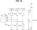
- FIG. 10 is a diagram showing a circuit configuration of an alternator using the semiconductor devices 200, 300 according to the first and second embodiments of the present invention to rectify output of a three-phase AC generator 801.
- the alternator 850 includes the AC generator 801 generating three-phase AC voltages Vu, Vv, Vw, having three output terminals 801u, 801v, 801w and the semiconductor devices 200 and 300 as rectifying elements for full-wave rectifying, and the capacitor 81 for smoothing.
- the output terminal 801u of the AC generator 801 is connected to a joint between the semiconductor devices 200 and 300 for U-phase.
- the output terminal 801v of the AC generator 801 is connected to a joint between the semiconductor devices 200 and 300 for V-phase.
- the output terminal 801w of the AC generator 801 is connected to a joint between the semiconductor devices 200 and 300 for W-phase.
- the alternator 850 outputs a DC output between the terminals 81p and 81m.
- the alternator 850 include a forward semiconductor device 200 comprising the semiconductor device 200 of which the one of the first internal electrode 14 and the second internal electrode 15 is the first internal electrode 14, and the reverse semiconductor device comprising the semiconductor device 300 of which the one of the first internal electrode and the second internal electrode is the second internal electrode 15; and the generator 801 generating an AC voltage, wherein the AC voltage is supplied between the forward semiconductor device and the reverse semiconductor device to generate a DC voltage.
- the three-phase full-wave rectification circuit device 800 is provided for full-wave rectification.
- omission of some components in the three-phase full-wave rectification circuit device 800 can provide a half-wave rectifier.
- the forward semiconductor device 200 for V-phase and the forward semiconductor device 200 for W-phase, the rearward semiconductor device 300 for U-phase, and rearward semiconductor device 300 for W-phase are omitted.
- the rearward semiconductor device 300 for V-phase can be omitted by short-circuiting between both terminal of the rearward semiconductor device 300 for V-phase. This provides a half-wave rectifier to output a DC voltage between the 81p and 81m.
Landscapes
- Engineering & Computer Science (AREA)
- Power Engineering (AREA)
- Rectifiers (AREA)
- Semiconductor Integrated Circuits (AREA)
- Physics & Mathematics (AREA)
- Geometry (AREA)
- Microelectronics & Electronic Packaging (AREA)
- Junction Field-Effect Transistors (AREA)
- Lead Frames For Integrated Circuits (AREA)
Applications Claiming Priority (1)
| Application Number | Priority Date | Filing Date | Title |
|---|---|---|---|
| JP2015225258A JP6641161B2 (ja) | 2015-11-18 | 2015-11-18 | 半導体装置、およびそれを用いたオルタネータ |
Publications (3)
| Publication Number | Publication Date |
|---|---|
| EP3171401A2 true EP3171401A2 (de) | 2017-05-24 |
| EP3171401A3 EP3171401A3 (de) | 2017-06-28 |
| EP3171401B1 EP3171401B1 (de) | 2020-06-24 |
Family
ID=57354161
Family Applications (1)
| Application Number | Title | Priority Date | Filing Date |
|---|---|---|---|
| EP16199336.5A Active EP3171401B1 (de) | 2015-11-18 | 2016-11-17 | Drehstromgenerator umfassend halbleiterbauelemente |
Country Status (5)
| Country | Link |
|---|---|
| US (1) | US10304761B2 (de) |
| EP (1) | EP3171401B1 (de) |
| JP (1) | JP6641161B2 (de) |
| CN (1) | CN106711137B (de) |
| TW (1) | TWI608589B (de) |
Cited By (1)
| Publication number | Priority date | Publication date | Assignee | Title |
|---|---|---|---|---|
| EP4156247A3 (de) * | 2021-09-07 | 2023-06-14 | Hitachi Power Semiconductor Device, Ltd. | Halbleiterbauelement mit einem zwischen einer ersten, plattenförmigen elektrode mit einer rille und einer zweiten elektrode verbundenen halbleiterchip |
Families Citing this family (14)
| Publication number | Priority date | Publication date | Assignee | Title |
|---|---|---|---|---|
| JP2018191995A (ja) * | 2017-05-17 | 2018-12-06 | 株式会社三洋物産 | 遊技機 |
| JP2018191994A (ja) * | 2017-05-17 | 2018-12-06 | 株式会社三洋物産 | 遊技機 |
| JP2018191991A (ja) * | 2017-05-17 | 2018-12-06 | 株式会社三洋物産 | 遊技機 |
| JP7250298B2 (ja) * | 2017-05-17 | 2023-04-03 | 株式会社三洋物産 | 遊技機 |
| JP7250297B2 (ja) * | 2017-05-17 | 2023-04-03 | 株式会社三洋物産 | 遊技機 |
| JP7131903B2 (ja) * | 2017-12-08 | 2022-09-06 | ローム株式会社 | 半導体パッケージ |
| JP6988518B2 (ja) * | 2018-01-26 | 2022-01-05 | 株式会社デンソー | 整流装置及び回転電機 |
| WO2019229829A1 (ja) * | 2018-05-29 | 2019-12-05 | 新電元工業株式会社 | 半導体モジュール |
| TWI710138B (zh) * | 2018-06-21 | 2020-11-11 | 朋程科技股份有限公司 | 用於整流器的功率元件 |
| JP7252248B2 (ja) * | 2018-10-15 | 2023-04-04 | ローム株式会社 | 半導体装置 |
| JP7231407B2 (ja) * | 2018-12-27 | 2023-03-01 | 株式会社 日立パワーデバイス | 半導体装置およびそれを用いたオルタネータ |
| JP7489181B2 (ja) * | 2019-11-11 | 2024-05-23 | 株式会社 日立パワーデバイス | 半導体装置 |
| JP7766507B2 (ja) * | 2022-02-03 | 2025-11-10 | ルネサスエレクトロニクス株式会社 | 半導体装置および回路装置 |
| TWI836903B (zh) * | 2023-02-16 | 2024-03-21 | 朋程科技股份有限公司 | 能量轉換模組與能量轉換裝置 |
Citations (3)
| Publication number | Priority date | Publication date | Assignee | Title |
|---|---|---|---|---|
| JPH05326830A (ja) | 1992-05-15 | 1993-12-10 | Fuji Electric Co Ltd | 半導体素子 |
| JP2001156225A (ja) | 1999-11-24 | 2001-06-08 | Denso Corp | 半導体装置 |
| JP2015116053A (ja) | 2013-12-12 | 2015-06-22 | 株式会社日立製作所 | 半導体装置、並びにそれを用いたオルタネータ及び電力変換装置 |
Family Cites Families (17)
| Publication number | Priority date | Publication date | Assignee | Title |
|---|---|---|---|---|
| JP2858166B2 (ja) * | 1990-10-08 | 1999-02-17 | 株式会社日立製作所 | 半導体整流素子及びそれを使った全波整流装置 |
| DE4120394A1 (de) * | 1991-06-20 | 1992-12-24 | Bosch Gmbh Robert | Monolithisch integrierte schaltungsanordnung |
| JP2002217416A (ja) * | 2001-01-16 | 2002-08-02 | Hitachi Ltd | 半導体装置 |
| DK1610708T3 (da) * | 2003-04-03 | 2020-02-24 | Align Technology Inc | Fremgangsmåde og system til fabrikation af en tandkappe |
| JP2006073655A (ja) * | 2004-08-31 | 2006-03-16 | Toshiba Corp | 半導体モジュール |
| JP2006222298A (ja) * | 2005-02-10 | 2006-08-24 | Renesas Technology Corp | 半導体装置およびその製造方法 |
| US20060220218A1 (en) * | 2005-03-11 | 2006-10-05 | Charng-Geng Sheen | Embedded-type power semiconductor package device |
| KR100772898B1 (ko) * | 2006-07-10 | 2007-11-05 | 삼성전자주식회사 | 반도체 집적 회로 장치의 제조 방법과 그에 의해 제조된 반도체 집적 회로 장치 |
| JP2008282867A (ja) * | 2007-05-08 | 2008-11-20 | Sharp Corp | 電力半導体装置、電子機器及びリードフレーム部材並びに電力半導体装置の製造方法 |
| JP5352113B2 (ja) * | 2008-04-22 | 2013-11-27 | トヨタ自動車株式会社 | インバータモジュール |
| JP5286150B2 (ja) * | 2009-04-23 | 2013-09-11 | 株式会社日本自動車部品総合研究所 | 電力変換用半導体装置 |
| JP5115595B2 (ja) * | 2010-06-23 | 2013-01-09 | 株式会社デンソー | 半導体モジュールの製造方法 |
| JP2013183024A (ja) * | 2012-03-01 | 2013-09-12 | Toyota Industries Corp | 半導体デバイスおよび半導体装置 |
| WO2014073483A1 (ja) * | 2012-11-08 | 2014-05-15 | シャープ株式会社 | アクティブマトリクス基板、及びこれを用いた表示装置 |
| JP2015095560A (ja) * | 2013-11-12 | 2015-05-18 | 株式会社デンソー | パワーモジュール |
| JP6407756B2 (ja) * | 2014-03-31 | 2018-10-17 | 株式会社東芝 | 半導体モジュールの製造方法 |
| DE102015011718A1 (de) * | 2014-09-10 | 2016-03-10 | Infineon Technologies Ag | Gleichrichtervorrichtung und Anordnung von Gleichrichtern |
-
2015
- 2015-11-18 JP JP2015225258A patent/JP6641161B2/ja active Active
-
2016
- 2016-11-14 CN CN201611020685.1A patent/CN106711137B/zh active Active
- 2016-11-17 EP EP16199336.5A patent/EP3171401B1/de active Active
- 2016-11-17 US US15/354,474 patent/US10304761B2/en active Active
- 2016-11-18 TW TW105137893A patent/TWI608589B/zh active
Patent Citations (3)
| Publication number | Priority date | Publication date | Assignee | Title |
|---|---|---|---|---|
| JPH05326830A (ja) | 1992-05-15 | 1993-12-10 | Fuji Electric Co Ltd | 半導体素子 |
| JP2001156225A (ja) | 1999-11-24 | 2001-06-08 | Denso Corp | 半導体装置 |
| JP2015116053A (ja) | 2013-12-12 | 2015-06-22 | 株式会社日立製作所 | 半導体装置、並びにそれを用いたオルタネータ及び電力変換装置 |
Cited By (2)
| Publication number | Priority date | Publication date | Assignee | Title |
|---|---|---|---|---|
| EP4156247A3 (de) * | 2021-09-07 | 2023-06-14 | Hitachi Power Semiconductor Device, Ltd. | Halbleiterbauelement mit einem zwischen einer ersten, plattenförmigen elektrode mit einer rille und einer zweiten elektrode verbundenen halbleiterchip |
| US12327808B2 (en) | 2021-09-07 | 2025-06-10 | Hitachi Power Semiconductor Device, Ltd. | Semiconductor device |
Also Published As
| Publication number | Publication date |
|---|---|
| TWI608589B (zh) | 2017-12-11 |
| CN106711137A (zh) | 2017-05-24 |
| US20170141018A1 (en) | 2017-05-18 |
| CN106711137B (zh) | 2019-03-08 |
| JP6641161B2 (ja) | 2020-02-05 |
| EP3171401B1 (de) | 2020-06-24 |
| EP3171401A3 (de) | 2017-06-28 |
| TW201719856A (zh) | 2017-06-01 |
| JP2017098276A (ja) | 2017-06-01 |
| US10304761B2 (en) | 2019-05-28 |
Similar Documents
| Publication | Publication Date | Title |
|---|---|---|
| EP3171401B1 (de) | Drehstromgenerator umfassend halbleiterbauelemente | |
| CN106158839B (zh) | 半导体器件 | |
| US9025341B2 (en) | Power converter | |
| CN207233730U (zh) | 电子装置 | |
| US9806029B2 (en) | Transistor arrangement with semiconductor chips between two substrates | |
| US10027094B2 (en) | Power module, power converter and drive arrangement with a power module | |
| CN105874596A (zh) | 半导体模块 | |
| US8804340B2 (en) | Power semiconductor package with double-sided cooling | |
| JP2002095268A (ja) | 電力変換装置 | |
| US20200027957A1 (en) | Semiconductor device | |
| US10943891B2 (en) | Semiconductor module and power conversion apparatus | |
| CN114846599A (zh) | 功率模块、电力转换装置及功率模块的制造方法 | |
| US20170213783A1 (en) | Multi-chip semiconductor power package | |
| JP2015095560A (ja) | パワーモジュール | |
| JP7045978B2 (ja) | 半導体装置および電力変換装置 | |
| CN112582356B (zh) | 半导体器件 | |
| CN104518681A (zh) | 电力变换装置 | |
| JP2015186438A (ja) | 半導体装置 | |
| US6844614B2 (en) | Semiconductor integrated circuit | |
| CN114144965A (zh) | 电路装置 | |
| JP2010016926A (ja) | 電力半導体モジュールおよびこれを備えた半導体電力変換装置 | |
| US20250112143A1 (en) | Semiconductor device, semiconductor module and manufacturing method | |
| JP6475660B2 (ja) | パワー半導体装置 |
Legal Events
| Date | Code | Title | Description |
|---|---|---|---|
| PUAI | Public reference made under article 153(3) epc to a published international application that has entered the european phase |
Free format text: ORIGINAL CODE: 0009012 |
|
| STAA | Information on the status of an ep patent application or granted ep patent |
Free format text: STATUS: REQUEST FOR EXAMINATION WAS MADE |
|
| 17P | Request for examination filed |
Effective date: 20161209 |
|
| AK | Designated contracting states |
Kind code of ref document: A2 Designated state(s): AL AT BE BG CH CY CZ DE DK EE ES FI FR GB GR HR HU IE IS IT LI LT LU LV MC MK MT NL NO PL PT RO RS SE SI SK SM TR |
|
| AX | Request for extension of the european patent |
Extension state: BA ME |
|
| PUAL | Search report despatched |
Free format text: ORIGINAL CODE: 0009013 |
|
| AK | Designated contracting states |
Kind code of ref document: A3 Designated state(s): AL AT BE BG CH CY CZ DE DK EE ES FI FR GB GR HR HU IE IS IT LI LT LU LV MC MK MT NL NO PL PT RO RS SE SI SK SM TR |
|
| AX | Request for extension of the european patent |
Extension state: BA ME |
|
| RIC1 | Information provided on ipc code assigned before grant |
Ipc: H01L 23/051 20060101AFI20170519BHEP |
|
| STAA | Information on the status of an ep patent application or granted ep patent |
Free format text: STATUS: EXAMINATION IS IN PROGRESS |
|
| 17Q | First examination report despatched |
Effective date: 20180214 |
|
| RIC1 | Information provided on ipc code assigned before grant |
Ipc: H01L 23/31 20060101ALI20191126BHEP Ipc: H01L 23/051 20060101AFI20191126BHEP Ipc: H01L 23/495 20060101ALI20191126BHEP |
|
| GRAP | Despatch of communication of intention to grant a patent |
Free format text: ORIGINAL CODE: EPIDOSNIGR1 |
|
| STAA | Information on the status of an ep patent application or granted ep patent |
Free format text: STATUS: GRANT OF PATENT IS INTENDED |
|
| INTG | Intention to grant announced |
Effective date: 20200116 |
|
| GRAS | Grant fee paid |
Free format text: ORIGINAL CODE: EPIDOSNIGR3 |
|
| GRAA | (expected) grant |
Free format text: ORIGINAL CODE: 0009210 |
|
| STAA | Information on the status of an ep patent application or granted ep patent |
Free format text: STATUS: THE PATENT HAS BEEN GRANTED |
|
| AK | Designated contracting states |
Kind code of ref document: B1 Designated state(s): AL AT BE BG CH CY CZ DE DK EE ES FI FR GB GR HR HU IE IS IT LI LT LU LV MC MK MT NL NO PL PT RO RS SE SI SK SM TR |
|
| REG | Reference to a national code |
Ref country code: GB Ref legal event code: FG4D |
|
| REG | Reference to a national code |
Ref country code: CH Ref legal event code: EP |
|
| REG | Reference to a national code |
Ref country code: AT Ref legal event code: REF Ref document number: 1284747 Country of ref document: AT Kind code of ref document: T Effective date: 20200715 |
|
| REG | Reference to a national code |
Ref country code: DE Ref legal event code: R096 Ref document number: 602016038615 Country of ref document: DE |
|
| REG | Reference to a national code |
Ref country code: IE Ref legal event code: FG4D |
|
| PG25 | Lapsed in a contracting state [announced via postgrant information from national office to epo] |
Ref country code: LT Free format text: LAPSE BECAUSE OF FAILURE TO SUBMIT A TRANSLATION OF THE DESCRIPTION OR TO PAY THE FEE WITHIN THE PRESCRIBED TIME-LIMIT Effective date: 20200624 Ref country code: FI Free format text: LAPSE BECAUSE OF FAILURE TO SUBMIT A TRANSLATION OF THE DESCRIPTION OR TO PAY THE FEE WITHIN THE PRESCRIBED TIME-LIMIT Effective date: 20200624 Ref country code: GR Free format text: LAPSE BECAUSE OF FAILURE TO SUBMIT A TRANSLATION OF THE DESCRIPTION OR TO PAY THE FEE WITHIN THE PRESCRIBED TIME-LIMIT Effective date: 20200925 Ref country code: NO Free format text: LAPSE BECAUSE OF FAILURE TO SUBMIT A TRANSLATION OF THE DESCRIPTION OR TO PAY THE FEE WITHIN THE PRESCRIBED TIME-LIMIT Effective date: 20200924 Ref country code: SE Free format text: LAPSE BECAUSE OF FAILURE TO SUBMIT A TRANSLATION OF THE DESCRIPTION OR TO PAY THE FEE WITHIN THE PRESCRIBED TIME-LIMIT Effective date: 20200624 |
|
| REG | Reference to a national code |
Ref country code: LT Ref legal event code: MG4D |
|
| PG25 | Lapsed in a contracting state [announced via postgrant information from national office to epo] |
Ref country code: HR Free format text: LAPSE BECAUSE OF FAILURE TO SUBMIT A TRANSLATION OF THE DESCRIPTION OR TO PAY THE FEE WITHIN THE PRESCRIBED TIME-LIMIT Effective date: 20200624 Ref country code: RS Free format text: LAPSE BECAUSE OF FAILURE TO SUBMIT A TRANSLATION OF THE DESCRIPTION OR TO PAY THE FEE WITHIN THE PRESCRIBED TIME-LIMIT Effective date: 20200624 Ref country code: LV Free format text: LAPSE BECAUSE OF FAILURE TO SUBMIT A TRANSLATION OF THE DESCRIPTION OR TO PAY THE FEE WITHIN THE PRESCRIBED TIME-LIMIT Effective date: 20200624 Ref country code: BG Free format text: LAPSE BECAUSE OF FAILURE TO SUBMIT A TRANSLATION OF THE DESCRIPTION OR TO PAY THE FEE WITHIN THE PRESCRIBED TIME-LIMIT Effective date: 20200924 |
|
| REG | Reference to a national code |
Ref country code: NL Ref legal event code: MP Effective date: 20200624 |
|
| REG | Reference to a national code |
Ref country code: AT Ref legal event code: MK05 Ref document number: 1284747 Country of ref document: AT Kind code of ref document: T Effective date: 20200624 |
|
| PG25 | Lapsed in a contracting state [announced via postgrant information from national office to epo] |
Ref country code: NL Free format text: LAPSE BECAUSE OF FAILURE TO SUBMIT A TRANSLATION OF THE DESCRIPTION OR TO PAY THE FEE WITHIN THE PRESCRIBED TIME-LIMIT Effective date: 20200624 Ref country code: AL Free format text: LAPSE BECAUSE OF FAILURE TO SUBMIT A TRANSLATION OF THE DESCRIPTION OR TO PAY THE FEE WITHIN THE PRESCRIBED TIME-LIMIT Effective date: 20200624 |
|
| PG25 | Lapsed in a contracting state [announced via postgrant information from national office to epo] |
Ref country code: PT Free format text: LAPSE BECAUSE OF FAILURE TO SUBMIT A TRANSLATION OF THE DESCRIPTION OR TO PAY THE FEE WITHIN THE PRESCRIBED TIME-LIMIT Effective date: 20201026 Ref country code: SM Free format text: LAPSE BECAUSE OF FAILURE TO SUBMIT A TRANSLATION OF THE DESCRIPTION OR TO PAY THE FEE WITHIN THE PRESCRIBED TIME-LIMIT Effective date: 20200624 Ref country code: EE Free format text: LAPSE BECAUSE OF FAILURE TO SUBMIT A TRANSLATION OF THE DESCRIPTION OR TO PAY THE FEE WITHIN THE PRESCRIBED TIME-LIMIT Effective date: 20200624 Ref country code: AT Free format text: LAPSE BECAUSE OF FAILURE TO SUBMIT A TRANSLATION OF THE DESCRIPTION OR TO PAY THE FEE WITHIN THE PRESCRIBED TIME-LIMIT Effective date: 20200624 Ref country code: RO Free format text: LAPSE BECAUSE OF FAILURE TO SUBMIT A TRANSLATION OF THE DESCRIPTION OR TO PAY THE FEE WITHIN THE PRESCRIBED TIME-LIMIT Effective date: 20200624 Ref country code: ES Free format text: LAPSE BECAUSE OF FAILURE TO SUBMIT A TRANSLATION OF THE DESCRIPTION OR TO PAY THE FEE WITHIN THE PRESCRIBED TIME-LIMIT Effective date: 20200624 Ref country code: CZ Free format text: LAPSE BECAUSE OF FAILURE TO SUBMIT A TRANSLATION OF THE DESCRIPTION OR TO PAY THE FEE WITHIN THE PRESCRIBED TIME-LIMIT Effective date: 20200624 |
|
| PG25 | Lapsed in a contracting state [announced via postgrant information from national office to epo] |
Ref country code: SK Free format text: LAPSE BECAUSE OF FAILURE TO SUBMIT A TRANSLATION OF THE DESCRIPTION OR TO PAY THE FEE WITHIN THE PRESCRIBED TIME-LIMIT Effective date: 20200624 Ref country code: PL Free format text: LAPSE BECAUSE OF FAILURE TO SUBMIT A TRANSLATION OF THE DESCRIPTION OR TO PAY THE FEE WITHIN THE PRESCRIBED TIME-LIMIT Effective date: 20200624 Ref country code: IS Free format text: LAPSE BECAUSE OF FAILURE TO SUBMIT A TRANSLATION OF THE DESCRIPTION OR TO PAY THE FEE WITHIN THE PRESCRIBED TIME-LIMIT Effective date: 20201024 |
|
| REG | Reference to a national code |
Ref country code: DE Ref legal event code: R097 Ref document number: 602016038615 Country of ref document: DE |
|
| PG25 | Lapsed in a contracting state [announced via postgrant information from national office to epo] |
Ref country code: DK Free format text: LAPSE BECAUSE OF FAILURE TO SUBMIT A TRANSLATION OF THE DESCRIPTION OR TO PAY THE FEE WITHIN THE PRESCRIBED TIME-LIMIT Effective date: 20200624 |
|
| PLBE | No opposition filed within time limit |
Free format text: ORIGINAL CODE: 0009261 |
|
| STAA | Information on the status of an ep patent application or granted ep patent |
Free format text: STATUS: NO OPPOSITION FILED WITHIN TIME LIMIT |
|
| 26N | No opposition filed |
Effective date: 20210325 |
|
| PG25 | Lapsed in a contracting state [announced via postgrant information from national office to epo] |
Ref country code: MC Free format text: LAPSE BECAUSE OF FAILURE TO SUBMIT A TRANSLATION OF THE DESCRIPTION OR TO PAY THE FEE WITHIN THE PRESCRIBED TIME-LIMIT Effective date: 20200624 |
|
| REG | Reference to a national code |
Ref country code: CH Ref legal event code: PL |
|
| GBPC | Gb: european patent ceased through non-payment of renewal fee |
Effective date: 20201117 |
|
| PG25 | Lapsed in a contracting state [announced via postgrant information from national office to epo] |
Ref country code: LU Free format text: LAPSE BECAUSE OF NON-PAYMENT OF DUE FEES Effective date: 20201117 |
|
| REG | Reference to a national code |
Ref country code: BE Ref legal event code: MM Effective date: 20201130 |
|
| PG25 | Lapsed in a contracting state [announced via postgrant information from national office to epo] |
Ref country code: SI Free format text: LAPSE BECAUSE OF FAILURE TO SUBMIT A TRANSLATION OF THE DESCRIPTION OR TO PAY THE FEE WITHIN THE PRESCRIBED TIME-LIMIT Effective date: 20200624 Ref country code: LI Free format text: LAPSE BECAUSE OF NON-PAYMENT OF DUE FEES Effective date: 20201130 Ref country code: CH Free format text: LAPSE BECAUSE OF NON-PAYMENT OF DUE FEES Effective date: 20201130 |
|
| PG25 | Lapsed in a contracting state [announced via postgrant information from national office to epo] |
Ref country code: IE Free format text: LAPSE BECAUSE OF NON-PAYMENT OF DUE FEES Effective date: 20201117 |
|
| PG25 | Lapsed in a contracting state [announced via postgrant information from national office to epo] |
Ref country code: GB Free format text: LAPSE BECAUSE OF NON-PAYMENT OF DUE FEES Effective date: 20201117 |
|
| PG25 | Lapsed in a contracting state [announced via postgrant information from national office to epo] |
Ref country code: IS Free format text: LAPSE BECAUSE OF FAILURE TO SUBMIT A TRANSLATION OF THE DESCRIPTION OR TO PAY THE FEE WITHIN THE PRESCRIBED TIME-LIMIT Effective date: 20201024 Ref country code: TR Free format text: LAPSE BECAUSE OF FAILURE TO SUBMIT A TRANSLATION OF THE DESCRIPTION OR TO PAY THE FEE WITHIN THE PRESCRIBED TIME-LIMIT Effective date: 20200624 Ref country code: MT Free format text: LAPSE BECAUSE OF FAILURE TO SUBMIT A TRANSLATION OF THE DESCRIPTION OR TO PAY THE FEE WITHIN THE PRESCRIBED TIME-LIMIT Effective date: 20200624 Ref country code: CY Free format text: LAPSE BECAUSE OF FAILURE TO SUBMIT A TRANSLATION OF THE DESCRIPTION OR TO PAY THE FEE WITHIN THE PRESCRIBED TIME-LIMIT Effective date: 20200624 |
|
| PG25 | Lapsed in a contracting state [announced via postgrant information from national office to epo] |
Ref country code: MK Free format text: LAPSE BECAUSE OF FAILURE TO SUBMIT A TRANSLATION OF THE DESCRIPTION OR TO PAY THE FEE WITHIN THE PRESCRIBED TIME-LIMIT Effective date: 20200624 |
|
| PG25 | Lapsed in a contracting state [announced via postgrant information from national office to epo] |
Ref country code: BE Free format text: LAPSE BECAUSE OF NON-PAYMENT OF DUE FEES Effective date: 20201130 |
|
| REG | Reference to a national code |
Ref country code: DE Ref legal event code: R082 Ref document number: 602016038615 Country of ref document: DE Representative=s name: DENNEMEYER & ASSOCIATES RECHTSANWALTSGESELLSCH, DE Ref country code: DE Ref legal event code: R081 Ref document number: 602016038615 Country of ref document: DE Owner name: MINEBEA POWER SEMICONDUCTOR DEVICE INC., HITAC, JP Free format text: FORMER OWNER: HITACHI POWER SEMICONDUCTOR DEVICE, LTD., HITACHI-SHI, LBARAKI, JP |
|
| REG | Reference to a national code |
Ref country code: DE Ref legal event code: R079 Ref document number: 602016038615 Country of ref document: DE Free format text: PREVIOUS MAIN CLASS: H01L0023051000 Ipc: H10W0076138000 |
|
| PGFP | Annual fee paid to national office [announced via postgrant information from national office to epo] |
Ref country code: DE Payment date: 20251119 Year of fee payment: 10 |
|
| PGFP | Annual fee paid to national office [announced via postgrant information from national office to epo] |
Ref country code: IT Payment date: 20251125 Year of fee payment: 10 |
|
| PGFP | Annual fee paid to national office [announced via postgrant information from national office to epo] |
Ref country code: FR Payment date: 20251126 Year of fee payment: 10 |