EP3157058B1 - Light emitting device package and lighting apparatus having same - Google Patents
Light emitting device package and lighting apparatus having same Download PDFInfo
- Publication number
- EP3157058B1 EP3157058B1 EP16193981.4A EP16193981A EP3157058B1 EP 3157058 B1 EP3157058 B1 EP 3157058B1 EP 16193981 A EP16193981 A EP 16193981A EP 3157058 B1 EP3157058 B1 EP 3157058B1
- Authority
- EP
- European Patent Office
- Prior art keywords
- lead frame
- light emitting
- cavity
- emitting device
- boundary
- Prior art date
- Legal status (The legal status is an assumption and is not a legal conclusion. Google has not performed a legal analysis and makes no representation as to the accuracy of the status listed.)
- Active
Links
Images


Classifications
-
- H—ELECTRICITY
- H10—SEMICONDUCTOR DEVICES; ELECTRIC SOLID-STATE DEVICES NOT OTHERWISE PROVIDED FOR
- H10H—INORGANIC LIGHT-EMITTING SEMICONDUCTOR DEVICES HAVING POTENTIAL BARRIERS
- H10H20/00—Individual inorganic light-emitting semiconductor devices having potential barriers, e.g. light-emitting diodes [LED]
- H10H20/80—Constructional details
- H10H20/85—Packages
- H10H20/857—Interconnections, e.g. lead-frames, bond wires or solder balls
-
- H—ELECTRICITY
- H10—SEMICONDUCTOR DEVICES; ELECTRIC SOLID-STATE DEVICES NOT OTHERWISE PROVIDED FOR
- H10H—INORGANIC LIGHT-EMITTING SEMICONDUCTOR DEVICES HAVING POTENTIAL BARRIERS
- H10H20/00—Individual inorganic light-emitting semiconductor devices having potential barriers, e.g. light-emitting diodes [LED]
- H10H20/80—Constructional details
- H10H20/85—Packages
- H10H20/852—Encapsulations
- H10H20/853—Encapsulations characterised by their shape
-
- H—ELECTRICITY
- H10—SEMICONDUCTOR DEVICES; ELECTRIC SOLID-STATE DEVICES NOT OTHERWISE PROVIDED FOR
- H10H—INORGANIC LIGHT-EMITTING SEMICONDUCTOR DEVICES HAVING POTENTIAL BARRIERS
- H10H20/00—Individual inorganic light-emitting semiconductor devices having potential barriers, e.g. light-emitting diodes [LED]
- H10H20/80—Constructional details
- H10H20/85—Packages
- H10H20/855—Optical field-shaping means, e.g. lenses
- H10H20/856—Reflecting means
-
- H—ELECTRICITY
- H10—SEMICONDUCTOR DEVICES; ELECTRIC SOLID-STATE DEVICES NOT OTHERWISE PROVIDED FOR
- H10W—GENERIC PACKAGES, INTERCONNECTIONS, CONNECTORS OR OTHER CONSTRUCTIONAL DETAILS OF DEVICES COVERED BY CLASS H10
- H10W70/00—Package substrates; Interposers; Redistribution layers [RDL]
- H10W70/40—Leadframes
- H10W70/421—Shapes or dispositions
- H10W70/442—Shapes or dispositions of multiple leadframes in a single chip
-
- H—ELECTRICITY
- H10—SEMICONDUCTOR DEVICES; ELECTRIC SOLID-STATE DEVICES NOT OTHERWISE PROVIDED FOR
- H10W—GENERIC PACKAGES, INTERCONNECTIONS, CONNECTORS OR OTHER CONSTRUCTIONAL DETAILS OF DEVICES COVERED BY CLASS H10
- H10W90/00—Package configurations
-
- H—ELECTRICITY
- H10—SEMICONDUCTOR DEVICES; ELECTRIC SOLID-STATE DEVICES NOT OTHERWISE PROVIDED FOR
- H10W—GENERIC PACKAGES, INTERCONNECTIONS, CONNECTORS OR OTHER CONSTRUCTIONAL DETAILS OF DEVICES COVERED BY CLASS H10
- H10W90/00—Package configurations
- H10W90/811—Multiple chips on leadframes
-
- H—ELECTRICITY
- H10—SEMICONDUCTOR DEVICES; ELECTRIC SOLID-STATE DEVICES NOT OTHERWISE PROVIDED FOR
- H10H—INORGANIC LIGHT-EMITTING SEMICONDUCTOR DEVICES HAVING POTENTIAL BARRIERS
- H10H20/00—Individual inorganic light-emitting semiconductor devices having potential barriers, e.g. light-emitting diodes [LED]
- H10H20/80—Constructional details
- H10H20/85—Packages
- H10H20/8506—Containers
-
- H—ELECTRICITY
- H10—SEMICONDUCTOR DEVICES; ELECTRIC SOLID-STATE DEVICES NOT OTHERWISE PROVIDED FOR
- H10W—GENERIC PACKAGES, INTERCONNECTIONS, CONNECTORS OR OTHER CONSTRUCTIONAL DETAILS OF DEVICES COVERED BY CLASS H10
- H10W90/00—Package configurations
- H10W90/701—Package configurations characterised by the relative positions of pads or connectors relative to package parts
- H10W90/751—Package configurations characterised by the relative positions of pads or connectors relative to package parts of bond wires
- H10W90/756—Package configurations characterised by the relative positions of pads or connectors relative to package parts of bond wires between a chip and a stacked lead frame, conducting package substrate or heat sink
Definitions
- Embodiments relate to a light emitting device package and a lighting apparatus having the same.
- Light emitting devices as a kind of semiconductor device which converts electric energy into light, are under the spotlight as next generation light sources which replace the conventional fluorescent lamps, incandescent lamps, or the like.
- the light emitting diodes consume only the very low power compared to the incandescent lamps which generate light by heating tungsten or the fluorescent lamps which generate light by impacting ultraviolet rays generated through a high-voltage discharge on a fluorescent substance, since the light emitting diodes generate light using the semiconductor device.
- the light emitting diodes have a long service life, fast response characteristics, and environment-friendly features compared to the conventional light sources since the light emitting diodes generate light using a potential gap of the semiconductor device.
- the embodiments provide a light emitting device package which is capable of improving light extraction efficiency and a lighting apparatus having the same.
- the embodiments provide a light emitting device package which is capable of improving luminous flux and a lighting apparatus having the same.
- the light emitting device package includes a first lead frame; a second lead frame that is spaced apart from the first lead frame; a body that is coupled to the first lead frame and the second lead frame and includes a first cavity which exposes a portion of the upper surface of the first lead frame, a second cavity which exposes a portion of the upper surface of the second lead frame, and a spacer which is disposed between the first lead frame and the second frame; at least one light emitting device that is disposed in the first cavity; and a protection device that is disposed in the second cavity.
- the second cavity may be disposed on a first inside surface of the first cavity and the first inside surface may be connected to an upper surface of the spacer.
- An area of a bottom surface of the first cavity may be equal to or less than 40% of entire area of the body.
- the light emitting device package includes the first cavity that exposes the first lead frame on which the light emitting device is mounted and the second cavity that exposes the second lead frame on which a protection device is mounted and the area of the exposed first lead frame has a range between 20% and 40% of an entire area of the body. Therefore, the embodiment may be capable of improving loss of light which is absorbed into the first lead frame.
- the area of the exposed second lead frame has a range between 3% and 10% of the entire area of the body. Therefore, the embodiment may be capable of minimizing the loss of light.
- a curvature R of a fifth inside surface of the second cavity has a range between 0.1 mm and 0.3 mm. Therefore, the embodiment may be capable of improving the light extraction efficiency by improving a total reflection of light emitted from the light emitting device.
- a reflection molding portion covering the protection device is disposed in the second cavity and thus reflects light which is provided to the protection device and is lost. Therefore, the embodiment may be capable of further improving the light extraction efficiency.
- the reflection molding portion disposed on the protection device may extend to a wire bonding portion of the protection device which is positioned on a bottom surface of the first cavity on which the light emitting device is disposed. Therefore, the another embodiment may be capable of further improving the light extraction efficiency by reducing area of the lead frame exposed from the first cavity and reflecting light which is lost by the wire bonding portion and a wire.
- each of layers (films), regions, patterns or structures is (are) formed “on/over” or “under” a substrate
- each of layers (films), regions, pads or patterns the "on/over” or the "under” includes a case where each of layers (films), regions, patterns or structures is (are) both “directly” and “with another layer being inserted therebetween (indirectly)” formed “on/over” or “under” a substrate, each of layers (films), regions, pads, or patterns.
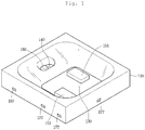
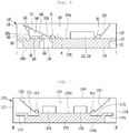
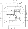
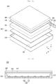
- Fig. 1 is a perspective view illustrating a light emitting device package according to a first embodiment and Fig. 2 is a plan view illustrating the light emitting device package according to the first embodiment.
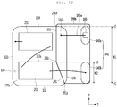
- Fig. 3 is a perspective view illustrating upper portions of a first lead frame and a second lead frame according to the first embodiment
- Fig. 4 is a perspective view illustrating lower portions of the first lead frame and the second lead frame according to the first embodiment
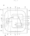
- Fig. 5 is a plan view illustrating the first lead frame and the second lead frame according to the first embodiment.
- Fig. 6 is a cross-sectional view illustrating the light emitting device package taking along line I-I' in Fig. 2
- Fig. 7 is a cross-sectional view illustrating the light emitting device package taking along line II-II' in Fig. 2 .
- a light emitting device package 110 may include a first lead frame 170, a second lead frame 180, a body 120, a protection device 160, and a first light emitting device 151 and a second light emitting device 153.
- the first lead frame 170 and the second frame 180 may be coupled to the body 120 in a state of being spaced apart from each other by a fixed distance.
- the first light emitting device 151 and the second light emitting device 153 may be mounted on the first lead frame 170 and the protection device 160 may be mounted on the second lead frame 180.
- a width of the first lead frame 170 may be greater than a width of the second lead frame 180.
- the first lead frame 170 and the second frame 180 may include conductive material.
- the first lead frame 170 and the second lead frame 180 may include at least one of titanium (Ti), copper (Cu), nickel (Ni), gold (Au), chrome (Cr), tantalum (Ta), platinum (Pt), tin (Sn), silver (Ag), phosphorus (P), iron (Fe), zinc (Zn), and aluminum (Al) and may be formed in a single layer or multiple layers.
- the first lead frame 170 may include an upper portion surface 170a on which the first light emitting device 151 and the second light emitting device 153 are mounted and a lower portion surface 170b which is exposed from a lower portion of the body 120.
- the upper portion surface 170a and the lower portion 170b of the first lead frame 170 may be flat surfaces.
- the first lead frame 170 may includes a first recess portion 171 which is disposed on the upper portion surface 170a of the first lead frame 170 and a first stepped portion 173 which is disposed on the lower portion surface 170b of the first lead frame 170.
- the first recess portion 171 may have a shape which is concave from the upper portion surface 170a of the first lead frame 170 in the direction of the lower portion surface 170b.
- the first recess portion 171 may be adjacent to an edge of the upper portion surface 170a.
- the first recess portion 171 may have a ring shape or a rectangular strip shape. However, it is not limited to this.
- the first recess portion 171 may have a round shape of which edges are bent. However, it is not limited to this.
- the first recess portion 171 may be improved a coupling force with the body 120 by increasing a contacting area with the body 120. Further, the first recess portion 171 may prevent external moisture penetration by a concave structure.
- the first recess portion 171 may be formed by being etched a portion of the upper portion surface 170a of the first lead frame 170. However, it is not limited to this. A depth of the first lead frame 171 may be 50% of a thickness of the first lead frame 170. However, it is not limited to this. For example, the depth of the first lead frame 171 may be equal to or less than 50% of the thickness of the first lead frame 170.
- the first recess portion 171 may be spaced apart from the first stepped portion 173 by a fixed distance. In other words, the first recess portion 171 may do not include a region which is vertically overlapped with the first stepped portion 173.
- the first recess portion 171 may be disposed on the outside of the first cavity 130 which exposes a portion of the upper portion of the first lead frame 170 from the body 120.
- the first recess portion 171 may be disposed on the inside of the first stepped portion 173.
- the first recess portion 171 may be disposed in the area which is between 5% and 30% of a minor axis width of the first lead frame 170 from the outside surface of the fist lead frame 170.
- a major axis of the first lead frame 170 is X-X' and the minor axis of the first lead frame 170 is Y-Y'.
- the first recess portion 171 In a case where the first recess portion 171 is disposed on an area which is less than 55 of the minor axis width of the first lead frame 170 from the outside surface of the first lead frame 170, the first recess portion 171 reduces a coupling force with the body 120 by reducing the width and the area of the first stepped portion 173 and thus may be difficult to prevent external moisture penetration. In a case where the first recess portion 171 is disposed on an area which is greater than 30% of the minor axis width of the first lead frame 170 from the outside surface of the first lead frame 170, the first recess portion 171 reduces a coupling force with the body 120 by a portion thereof being exposed to the first cavity 130 and thus may be difficult to prevent the external moisture penetration. For example, in a case where the minor width of the first lead frame 170 is 1,920 mm, the first recess portion 171 may be disposed in the region spaced apart from an adjacent outside surface of the first lead frame 170.
- the first recess portion 171 may include a fixed width.
- the first recess frame 171 may include 3% to 15% of width of the minor axis width of the first lead frame 170.
- the width of the first recess portion 171 is equal to or less than 3% of the minor axis width of the first lead frame 170
- the first recess portion 171 reduces a coupling force with the body 120 by reducing a contacting area with the body 120 and thus may be difficult to prevent the external moisture penetration.
- the width of the first recess portion 171 is greater than 15% of the minor axis width of the first lead frame 170, rigidity of the first lead frame 170 may be reduced.
- the width of the first recess portion 171 may be between 50 ⁇ m and 290 ⁇ m.
- the first stepped portion 173 may be disposed on the edge of the lower portion surface 170b of the first lead frame 170.
- the first stepped portion 173 may be connected along the edge of the lower portion surface 170b of the first lead frame 170.
- the first stepped portion 173 may has a recess shape and a cross-sectional surface thereof may have a stepped structure. However, it is not limited to this.
- the first stepped portion 173 may be improved a coupling force with the body 120 by increasing a contacting area with the body 120. Further, the first stepped portion 173 may prevent the external moisture penetration by a stepped structure.
- the first stepped portion 173 may be formed by being etched a portion of an edge of the lower portion surface 170b of the first lead frame 170.
- a thickness of the first stepped frame 173 may be 50% of the thickness of the first lead frame 170. However, it is not limited to this. For example, the thickness of the first stepped frame 173 may be equal to or greater than 50% of the thickness of the first lead frame 170.
- the first stepped portion 173 may be further disposed on the outside than the first recess portion 171.
- the first lead frame 170 may include first projecting portions 177 projected in the outside direction.
- the first recess portions 177 may be spaced apart from the first stepped portion 173 in the outside direction.
- the thickness of the first projections 177 may be thinner than the thickness of the first lead frame 170.
- the horizontal width of each of the first projecting portions 177 may be different from each other. However, it is not limited to this.
- the ends of the first projecting portions 177 may be exposed from the outside surface of the body 120 to the outside.
- units of the first lead frame 170 and the second lead frame 180 are made by processing a metal frame (not illustrated) with a press and then may be separated from a state where a plurality of the first lead frames 170 and a plurality of the second lead frames 180 are connected with each other after the injection process of the body 120.
- the plurality of the first lead frames 170 and the plurality of the second lead frames 180 may be include a hanger (not illustrated) for connecting the plurality of the first lead frames 170 and the plurality of the second lead frames 180 with each other since the injection process for coupling the bodies 120 connected with each other proceeds.
- the first projecting portions 177 may be a portion of the hanger connected to the first lead frame 170 in a separating process into units of the first lead frame 170 and the second lead frame 180.
- the first lead frame 180 may include an upper portion surface 180a on which the protection device 160 is mounted and a lower portion surface 180b which is exposed from a lower portion of the body 120.
- the upper portion surface 180a and the lower portion 180b of the second lead frame 180 may be flat surfaces.
- the second lead frame 180 may includes a second recess portion 181 which is disposed on the upper portion surface 180a of the second lead frame 180 and a second stepped portion 183 which is disposed on the lower portion surface 180b of the second lead frame 180.
- the second recess portion 181 may have a shape which is concave from the upper portion surface 180a of the second lead frame 180 in the direction of the lower portion surface 180b.
- the second recess portion 181 may be adjacent to the edge of the upper portion surface 180a of the second lead frame 180.
- the second recess portion 181 may be disposed to be parallel in the longitudinal direction of the second lead frame 180.
- the second recess portion 181 may have both ends which have a bent shape. However, it is not limited to this.
- the second recess portion 181 may includes have both ends which have a bent shape to face each other. However, it is not limited to this.
- the second recess portion 181 may be improved a coupling force with the body 120 by increasing a contacting area with the body 120. Further, the second recess portion 181 may prevent the external moisture penetration by a concave structure.
- the second recess portion 181 may be formed by etching a portion of the upper portion surface 180a of the second lead frame 180. However, it is not limited to this. A depth of the second lead frame 181 may be 50% of a thickness of the second lead frame 180. However, it is not limited to this. For example, the depth of the second lead frame 181 may be equal to or less than 50% of a thickness of the second lead frame 180.
- the second recess portion 181 may be spaced apart from the second stepped portion 183 by a fixed distance. In other words, the second recess portion 181 may not include a region which is vertically overlapped with the second stepped portion 183.
- the second recess portion 181 may be disposed on the outside of the second cavity 140 which exposes the portion of the upper portion of the second lead frame 180 from the body 120.
- the second recess portion 181 may be disposed on the inside of the second stepped portion 183.
- the both ends 180e of the second recess portion 181 may be disposed in the area which is between 15% and 85% of a minor axis width of the second lead frame 180 from the outside surface of the second lead frame 180 which is furthest from the first lead frame 170.
- a major axis of the second lead frame 180 is X-X' and the minor axis of the second lead frame 180 is Y-Y'.
- the second recess portion 171 reduces a coupling force with the body 120 by reducing the width and the area of the second stepped portion 183 and thus may be difficult to prevent the external moisture penetration.
- the second recess portion 181 is disposed on an area which is greater than 85% of the minor axis width of the second lead frame 180 from the outside surface of the second lead frame 180, a portion of the second recess portion 181 is exposed to the second cavity 140 or the second recess portion 171 is reduced a coupling force with the body 120 by reducing the width and the area of the second stepped portion 183 and thus may be difficult to prevent the external moisture penetration.
- both ends 180e of the second recess portion 181 may be disposed in the region spaced apart by 180 ⁇ m to 580 ⁇ m from the outside surface of the second lead frame 180 which is furthest from the first lead frame 170.
- the second recess portion 181 may include a fixed width.
- the second recess portion 181 may include 7% to 43% of width of the minor axis width of the second lead frame 180 from the body 120.
- the second recess portion 181 reduces a coupling force with the body 120 by reducing a contacting area with the body 120 and thus may be difficult to prevent external moisture penetration.
- the width of the second lead frame 181 is greater than 43% of the minor axis width of the second lead frame 180 and thus rigidity of the second lead frame 180 may be reduced.
- the width of the second recess portion 181 may be between 50 ⁇ m and 290 ⁇ m.
- the second recess portion 181 may include a rectilinear portion 1811, a bent portion 181c and both ends 181e along the major axis of the second recess portion 181 about a center portion C of the second recess portion 181.
- the bent portion 181c may be bent in a second direction Y of the minor axis of the second lead frame 180.
- the bent portion 181c may be spaced apart from the rectilinear portion 1811 by a fixed distance.
- the bent portion 181c may be disposed between 20% and 80% of a major axis length or width of the major axis of the second recess portion 181 from the center portion C of the second recess portion 181 in the major axis (X-X') direction of the second lead frame 180.
- a boundary region 181b between the bent portion 181c and the rectilinear portion 1811 may be disposed between 20% and 80% of the second recess portion 181 from the center portion C of the second recess portion 181 in the major axis (X-X') direction of the second lead frame 180.
- the second stepped portion 183 may be disposed on the edge of the lower portion surface 180b of the second lead frame 180.
- the second stepped portion 183 may be connected along the edge of the lower portion surface of the second lead frame 180.
- the second stepped portion 183 may has a recess shape and a cross-sectional surface thereof may have a stepped structure. However, it is not limited to this.
- the second stepped portion 183 may be improved a coupling force with the body 120 by increasing a contacting area with the body 120. Further, the second stepped portion 183 may prevent the external moisture penetration by a stepped structure.
- the second stepped portion 183 may be formed by being etched a portion of an edge of the lower portion surface 180b of the second lead frame 180. However, it is not limited to this.
- a thickness of the second stepped frame 183 may be 50% of the thickness of the second lead frame 180. However, it is not limited to this. For example, the thickness of the second stepped frame 183 may be equal to or greater than 50% of the thickness of the second lead frame 180.
- the second stepped portion 183 may be further disposed on the outer than the second stepped portion 181.
- the second lead frame 180 may include second projecting portions 187 projected in the outside direction.
- the second recess portions 187 may be projected from the third stepped portion 183 in the outside direction.
- the thickness of the second projections 187 may be thinner than the thickness of the second lead frame 180.
- the horizontal width of each of the second projecting portions 187 may be different from each other. However, it is not limited to this.
- the ends of the second projecting portions 187 may be exposed from the outside surface of the body 120 to the outside.
- the second projecting portions 187 may be a portion of the hanger connected to the second lead frame 180 in a separating process into units of the first lead frame 180 and the second lead frame 180.
- the first light emitting device 151 and the second light emitting device 153 may be disposed on the first lead frame 170.
- the first light emitting device 151 and the second light emitting device 153 may be disposed on the upper portion surface of the first lead frame 170 which is exposed from the body 120. Even if the first light emitting device 151 and the second light emitting device 153 according to the embodiment is described as two configurations connected to each other in series, it is not limited to this. In other words, they may be a single configuration, may be configured to be in an array form, or may be at least three configurations.
- the first light emitting device 151 and the second light emitting device 153 may be connected through a wire W1. However, it is not limited to this.
- the first light emitting device 151 and the second light emitting device 153 is spaces apart from each other and the first light emitting device 151 and the second light emitting device 153 may be symmetrically disposed in a diagonal direction of the first lead frame 170 on the upper portion surface of the first lead frame 170 exposed from the body 120. However, it is not limited to this.
- the protection device 160 may be disposed on the second lead frame 180.
- the protection device 160 may be disposed on the upper portion surface of the second lead frame 180 which is exposed from the body 120.
- the protection device 160 may be a Zener diode, a thyristor, a transient voltage suppression (TVS), or the like. However, it is not limited to this.
- the protection device 160 according to the embodiment describes the Zener diode which protects the first light emitting device 151 and the second light emitting device 153 from electro static discharge (ESD) as an example.
- ESD electro static discharge
- the protection device 160 may be connected to the first lead frame 170 through a wire W2.
- the body 120 may include at least one of translucent material, reflective material, and insulating material.
- the body 120 may include material of which reflectivity is higher than permeability, for light emitted from the first light emitting device 151 and the second light emitting device 153.
- the body 120 may be resin based insulating material.
- the body 120 may be made of at least one of polyphthalamide (PPA), resin material such as epoxy or silicone material, silicon (Si), metallic material, photo sensitive glass (PSG), sapphire (Al 2 O 3 ), a printed circuit board (PCB), for example.
- PPA polyphthalamide
- resin material such as epoxy or silicone material
- silicon (Si) silicon
- metallic material silicon
- PSG photo sensitive glass
- Al 2 O 3 a printed circuit board
- the body 120 may include an outside surface having a fixed curvature or an outside surface having an angled surface.
- a plan view shape of the body may be a circular shape or a polygonal shape, for example.
- the body 120 may be coupled with the first lead frame 170 and the second lead frame 180.
- the body 120 may include a first cavity 130 which exposes a portion of the upper portion of the first lead frame 170.
- the body 120 may include a spacer 126 which is disposed between the first lead frame 170 and the second lead frame 180.
- the spacer 126 may be disposed on the bottom surface of the first cavity 130.
- the spacer 126 may be disposed to be parallel to the first stepped portion 173 and the second stepped portion 183 which face each other.
- the spacer 126 may be directly in contact with the first stepped portion 173 and the second stepped portion 183.
- the spacer 126 may be made of insulating material and may be a portion of the body 120. However, it is not limited to this.
- the spacer 126 includes a stepped structure which corresponds to the stepped structure of the first stepped portion 173 and the second stepped portion 183.
- the cross-section of the spacer 126 may have a step structure which is symmetric in the horizontal direction.
- the spacer 126 may be improved a coupling force since the contacting area with the first lead frame 170 and the second lead frame 180 increases by the stepped structure which is in contact with the first stepped portion 173 and the second stepped portion 183. Therefore, the embodiment is capable of preventing the external moisture penetration.
- the first cavity 130 may include a bottom surface which exposes the first lead frame 170 and a first inside surface 131 to the fourth inside surface 134 which positions along the edge of the exposed first lead frame 170.
- the first inside surface 131 may be disposed to face the third inside surface 133.
- the second inside portion 132 may be disposed to face the fourth inside surface 134.
- the first inside surface 131 to the fourth inside surface 134 may be disposed to be inclined from the bottom surface of the body 120.
- An area of the first lead frame 170 exposed to the bottom surface of the first cavity 130 may be less than 40% of an area surrounded by the first outside surface 121 to the fourth outside surface 124 of the body 120.
- the area of the first lead frame 170 exposed to the bottom surface of the first cavity 130 may be between 20% and 40% of an area surrounded by the first outside surface 121 to the fourth outside surface 124 of the body 120.
- the area of the first lead frame 170 exposed to the bottom surface of the first cavity 130 may be between 12% and 26% of the area surrounded by the first outside surface 121 to the fourth outside surface 124 of the body 120.
- the area surrounded by the first outside surface 121 to the fourth outside surface 124 of the body 120 may be 3.0 mm x 3.0 mm
- the area of the first lead frame 170 exposed to the bottom surface of the first cavity 130 may be between 1.390 mm x 0.840 mm and 1.390 mm x 1.680 mm.
- the embodiment is capable of improving loss of light which is absorbed into the first lead frame 170, improving the light extraction efficiency, and increasing the luminous flex, by the area of the first lead frame 170 exposed to the bottom surface of the first cavity 130 having a range between 20% and 40% of the entire area of the body 120.
- the area of the first cavity 130 is less than 20%, a problem on the mounting process of the first light emitting device 151 and the second light emitting device 153 may be generated due to constraint of space for mounting of the first light emitting device 151 and the second emitting device 153.
- the reflectivity may be reduced since the area of the first inside surface 131 to the fourth inside surface 134 are reduced and light extraction may be reduced due to the light loss since the exposed area of the first lead frame 170 increases and thus the light of the first light emitting device 151 and the second light emitting device 153 is absorbed into the first lead frame 170.
- the first inside surface 131 and the third inside surface 133 of the first cavity 130 facing each other may have an inclined angle to the upper surface of the first lead frame 170 which are different from each other.
- the inclined angle ⁇ 1 of the first inside surface 131 may be greater than the inclined angle ⁇ 2 of the third inside surface 133.
- the embodiment may determine the inclined angle ⁇ 1 of the first inside surface 131 and the inclined angle ⁇ 2 of the third inside surface 133 which face each other according to the area of the first lead frame exposed to the bottom surface of the first cavity 130. For example, in a case where the area of the first lead frame 170 exposed to the bottom surface of the first cavity 130 increases between 20% and 30% of the entire area of the body 120, the inclined angle ⁇ 1 of the first inside surface 131 may be decreased from 160 degrees to 156 degrees and the inclined angle ⁇ 2 of the third inside surface 133 may be decreased from 140 degrees to 119 degrees.
- the second inside surface 132 and the fourth inside surface 134 may have the inclined angles to the upper surface of the first lead frame 170 which are the same to each other.
- An inclined angle ⁇ 3 of the second inside surface 132 may be the same as an inclined angle ⁇ 4 of the fourth inside surface 134. However, it is not limited to this.
- the body 120 may include a second cavity 140 which expose a portion of an upper surface of the second lead frame 180.
- the second cavity 140 may position on a first inside surface 131 of the first cavity 130.
- the second cavity 140 is capable of exposing a portion of an upper surface of the second lead frame 180 through the first inside surface 131.
- a plan view shape of the first cavity 140 may be a circular, an oval, a polygonal shape.
- An area of the second lead frame 180 exposed to the bottom surface of the second cavity 140 may be less than 20% of an area surrounded by the first outside surface 121 to the fourth outside surface 124 of the body 120.
- the area of the second lead frame 180 exposed to the bottom surface of the second cavity 140 may be between 3% and 20% of an area surrounded by the first outside surface 121 to the fourth outside surface 124 of the body 120.
- the embodiment is capable of improving loss of light which is absorbed into the second lead frame 180, improving the light extraction efficiency, and increasing luminous flex, by the area of the second lead frame 180 exposed to the bottom surface of the second cavity 140 having a range between 3% and 20% of the area surrounded by the first outside surface 121 to the fourth outside surface 124 of the body 120.
- the area of the second cavity 140 is less than 3%, a problem on the mounting process of the protection device 160 may be generated due to constraint of space for mounting of the protection device 160.
- the light extraction may be decreased by a reduction of reflectivity and light loss.
- the area surrounded by the first outside surface 121 to the fourth outside surface 124 of the body 120 may be 3.0 mm x 3.0 mm
- the area of the second lead frame 180 exposed to the bottom surface of the second cavity 140 may be between 0.350 mm x 0.140 mm and 2 to 1.390 mm x 1.680 mm.
- the second cavity 140 may include a bottom surface which exposes the second lead frame 180 and a fifth inside surface 141 to the eighth inside surface 144 which positions along the edge of the exposed second lead frame 180.
- the fifth inside portion 141 may be disposed to face the seventh inside surface 143.
- the fifth inside surface 141 may have a height which is greater than the height of the seventh inside surface 143.
- the sixth inside portion 142 may be disposed to face the eighth inside surface 144.
- the fifth inside surface 141 may have a fixed curvature R so that the light emitted from the first light emitting device 151 and the second light emitting device 153 on the fist inside surface 131 is reflected in the various directions.
- the curvature R of the fifth inside surface 141 may be in a range between 0.1 mm to 0.3 mm.
- the curvature R of the fifth inside surface 141 is capable of improving the light extraction efficiency by improving total reflection of light emitted from the first light emitting device 151 and the second light emitting device 153.
- the curvature R of the fifth inside surface 141 is less than 0.1 mm, the light emitted from the first light emitting device 151 and the second light emitting device 153 generates the light loss since being totally reflected by a critical angle.
- the curvature R of the fifth inside surface 141 is greater than 0.3 mm, a problem on the process may be generated due to restrictions about the thickness and the height of the body 120.
- the sixth inside surface 142 to the eighth inside surface 144 may have a fixed curvature. However, it is not limited to this.
- the sixth inside surface 142 to the eighth inside surface 144 may have a curvature only in a boundary region with the first inside surface 131 and also may have a curvature corresponding to the curvature of the fifth inside surface 141. Further, the curvatures of the sixth inside surface 141 and the eighth inside surface 144 may differ from each other.
- a boundary portion 131a may be disposed between the second cavity 140 and the first lead frame 170 exposed from the first cavity 130.
- the boundary portion 131a may be disposed in the first inside surface 131.
- the boundary portion 131a may be connected with the seventh inside surface 143 of the second cavity 140.
- the boundary portion 131a may be disposed on the spacer 126.
- the boundary portion 131a may be vertically overlapped with the spacer 126.
- the boundary portion 131a may have a height H so that an inside thereof facing the protection device 160 is higher than the protection device 160.
- the problem that light emitted from the first light emitting device 151 and the second light emitting device 153 is lost by directly being provided to the protection device 160 is capable of improving since the inside of the boundary portion 131a which is facing the protection device 160 has a height H which is higher than the height of the protection device 160.
- the height H of the boundary portion 131a may be between 100 ⁇ m and 300 ⁇ m and the height of the protection device 160 may be less than 100 ⁇ m.
- the light emitting device package 110 include the first cavity 130 which exposes the upper portion surface of the first lead frame 170 on which the first light emitting device 151 and the second light emitting device 153 are mounted and the second cavity 140 which exposes the upper portion surface of the second lead frame 180 on which the protection device 160 are mounted.
- the area of the first lead frame 170 exposed to the bottom surface of the first cavity 130 has a range between 20% and 40% of the entire area of the body 120 and thus loss of light absorbed into the first lead frame 170 may be prevented.
- the area of the second lead frame 180 exposed to the bottom surface of the second cavity 14 has a range between 3% and 10% of the entire area of the body 120 and thus the light loss due to the second cavity 140 is minimized.
- the curvature R of the fifth inside surface 141 of the second cavity 140 has a range between 0.1 mm and 0.3 mm. Therefore, the light extraction efficiency may be improved by improving the total reflection of right emitted from the first light emitting device 151 and the second light emitting device 153.
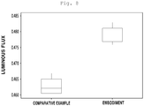
- Fig. 8 is a graph comparing a luminous flex in a comparative example to a luminous flex in the first embodiment.
- the luminous flex may be improved by at least 3.6% compared to the comparative example.
- the comparative example includes a body which has a cavity and a first lead frame and a second lead frame which are exposed to the bottom surface of the cavity and may be a structure in which an exposed area of the first lead frame and the second lead frame is greater than 50% of the entire area of the body.
- the embodiment is a light emitting device package adapting technical characteristics of Fig. 1 to Fig. 7 .
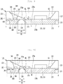
- Fig. 9 is a cross-sectional view illustrating a light emitting device package according to a second embodiment.
- the light emitting device package according to the second embodiment may adapt technical characteristics of the light emitting device package according to the first embodiment of the Fig. 1 to Fig. 7 , except for a boundary portion 231a.
- the boundary portion 231a may be disposed in a first inside surface 131.
- the boundary portion 231a is disposed on the space 126 and may disposed on a portion of the upper portion surface 170a of the first lead frame 170 which is in contact with the spacer 126 and a portion of the upper portion surface 180a of the second lead frame 180.
- the boundary portion 231a may have a height H which is higher than the protection device 160.
- the problem that light emitted from the first light emitting device 151 and the second light emitting device 153 is lost by directly being provided to the protection device 160 is capable of being improved since the boundary portion 231a has a height H which is higher than the height of the protection device 160.
- One end of the boundary portion 231a in the minor axis direction may be disposed to be more adjacent to the first light emitting device 151 and the second light emitting device 153 than one end of the spacer 126 in the minor axis direction.
- An opposite end of the boundary portion 231a in the minor axis direction may be disposed to be more adjacent to the protection device 160 than the opposite end of the spacer 126 in the minor axis direction.
- a width D1 of the boundary portion 231a in the minor axis direction may be greater than the width D2 of the spacer 126 in the minor axis direction.
- a width D1 of the boundary portion 231a in the minor axis direction may be equal to or greater than the width D2 the lower surface of the spacer 126 in the minor axis direction.
- the boundary portion 231a may be made of insulating material and may be a portion of the body 120. However, it is not limited to this.
- the boundary portion 231a may be made of the same material with the material of the spacer 126.
- the light emitting device package according to the second embodiment may improve a coupling force with the body 129 and prevent the external moisture penetration, by widening a contacting area with the body 120 by the structure of the boundary portion 231a covering the spacer 126.
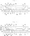
- Fig. 10 is a cross-sectional view illustrating the light emitting device package according to a third embodiment.
- the light emitting device package according to the third embodiment may adapt the technical characteristics of the light emitting device package according to the first embodiment according to the Fig. 1 to Fig. 7 , except for a boundary portion 331a.
- the boundary portion 331a may be disposed in a first inside surface 131.
- the boundary portion 331a is disposed on the space 126 and may disposed on a portion of the upper portion surface 170a of the first lead frame 170 which is in contact with the spacer 126 and a portion of the upper portion surface 180a of the second lead frame 180.
- the boundary portion 331a may have a height H which is higher than the protection device 160.
- the problem that light emitted from the first light emitting device 151 and the second light emitting device 153 is lost by directly being provided to the protection device 160 is capable of being improved since the boundary portion 331a has a height H which is higher than the height of the protection device 160.
- the boundary portion 331a may cover the upper portion surface of the spacer 126.
- a width D1 of the boundary portion 331a in the minor axis direction may be equal to or less than the width D2 of the spacer 126 in the minor axis direction.
- a width D1 of the boundary portion 331a in the minor axis direction may be equal than or less than the width D2 of the lower surface of the spacer 126 in the minor axis direction.
- the boundary portion 331a may be made of insulating material and may be a portion of the body 120. However, it is not limited to this.
- the boundary portion 331a may be made of the same material with the material of the spacer 126.
- the light emitting device package according to the third embodiment may improve a coupling force with the body 129 and prevent the external moisture penetration, by widening a contacting area with the body 120 due to the structure of the boundary portion 331a covering the spacer 126.
- Fig. 11 is a cross-sectional view illustrating the light emitting device package according to a fourth embodiment.
- the light emitting device package according to the fourth embodiment may adapt the technical characteristics of the light emitting device package according to the first embodiment of the Fig. 1 to Fig. 7 , except for a boundary portion 431a.
- the boundary portion 431a may be disposed in a first inside surface 131.
- the boundary portion 431a is disposed on the space 126 and may dispose on a portion of the upper portion surface 180a of the second lead frame 180 which is in contact with the spacer 126.
- a portion of the upper portion surface of the spacer 126 may expose from the boundary portion 431a.
- the boundary portion 431a may be not contact with the upper portion surface 170a of the first lead frame 170.
- the boundary portion 431a may have a height H which is higher than the protection device 160.
- the problem that light emitted from the first light emitting device 151 and the second light emitting device 153 is lost by directly being provided to the protection device 160 is capable of being improved since the boundary portion 431a has a height H which is higher than the height of the protection device 160.
- One end of the boundary portion 431a in the minor axis direction may be disposed on the upper surface of the spacer 126.
- One end of the boundary portion 431a in the minor axis direction may be disposed to be further away from the first light emitting device 151 and the second light emitting device 153 than the opposite one end of the spacer 126 in the minor axis direction by being disposed on the upper portion surface of the spacer 126.
- An opposite end of the boundary portion 431a in the minor axis direction may be disposed to be more adjacent to the protection device 160 than the opposite end of the spacer 126 in the minor axis direction.
- the light emitting device package according to the fourth embodiment may improve a coupling force with the body 129 and prevent the external moisture penetration, by widening a contacting area with the body 120 by the structure of the boundary portion 431a covering a portion of the spacer 126.
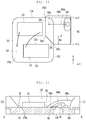
- Fig. 12 is a cross-sectional view illustrating the light emitting device package according to the fifth embodiment.
- the light emitting device package according to the fifth embodiment may adapt the technical characteristics of the light emitting device package according to the first embodiment of the Fig. 1 to Fig. 7 , except for a reflection molding portion 190.
- the reflection molding portion 190 may is disposed in the second cavity 140.
- the reflection molding portion 190 may cover the protection device 160.
- An upper portion surface 131a of the reflection molding portion 190 may be a position which is lower than the upper portion surface of the boundary portion 131a.
- the upper portion of the reflection molding portion 190 may be position on the same plane as the upper portion surface of the boundary portion 131a.
- a height of the reflection molding portion 190 may be higher than the height of the protection device 160.
- the height of the reflection molding portion 190 may be equal to or less than the height of the boundary portion 131a. However, it is not limited to this.
- the reflection molding portion 190 may include insulating material or reflective material.
- the reflection molding portion 190 may be made of at least one of polyphthalamide (PPA), poly-cyclo-hecylene dimethyl terephthalate (PCT), white silicone, and white epoxy molding compound (white EMC). However, it is not limited to this.
- the reflection molding portion 190 covering the protection device 160 is disposed in the second cavity 140 and reflects light which is absorbed into the protection device 160 and thus light extraction efficiency is capable of further improving.
- the light emitting device package has a structure in which the first light emitting device 151 and the second light emitting device 153 are disposed on the first cavity 130. However, it is not limited to this. In other words, the light emitting device package has a structure in which at least three light emitting devices are disposed on the first cavity 130.
- Fig. 13 to Fig. 22 are plan views or cross-sectional views illustrating light emitting device packages having another embodiments of reflection molding portions 290a to 290e.
- the light emitting device packages according to Fig 13 to Fig. 22 may adapt the technical characteristics of the light emitting device package according to the first embodiment of the Fig. 1 to Fig. 7 , except for the reflection molding portions 290a to 290e.
- a light emitting device package may improve the light extraction efficiency.
- the light emitting device packages according to another embodiment may include the reflection molding portion 290a to 290e.
- the reflection molding portions 290a to 290e are capable of covering the protection device 160, a first wire 160w, and a wire bonding portion 160a.
- the reflection molding portions 290a to 290e may cover the protection device 160 and the wire bonding portion 160a and cover a portion of the first wire 160w.
- the reflection molding portions 290a to 290e may reflect the light absorbed by the protection device 160, the first wire 160w, and the wire bonding portion 160a and thus the light extraction efficiency may be improved.
- the reflection molding portions 290a to 290e may have reflectivity which is greater than the reflectivity of the first lead frame 170.
- the reflection molding portions 290a to 290e extend to the upper portion surface 170a of the first lead frame 170 exposed to the first cavity 130 and thus are capable of improving the light extraction efficiency.
- the reflection molding portion 290a may be disposed on the second cavity 140.
- a portion of the reflection molding portion 290a may disposed on the upper portion surface 170a of the first lead frame 170 exposed from the first cavity 130.
- the reflection molding portion 290a may extend to the bottom surface of the first cavity 130 which is closest to the second cavity 140.
- the reflection molding portion 290a may cover a portion of the first inside surface 131 on which the second cavity 140 is disposed.
- the reflection molding portion 290a may extend to the wire bonding portion 160a of the protection device 160 disposed on the bottom surface of the first cavity 130 along the first inside surface 131 of the periphery of the second cavity 140.
- the reflection molding portion 290a may be disposed along the first inside surface 131 between the second cavity 140 and the first cavity 130.
- the wire bonding portion 160a may be disposed on the upper portion surface 170a of the first lead frame 170 exposed to the bottom surface of the first cavity 130 which is closest to the second cavity 140.
- the end 291 of the reflection molding portion 290a may be disposed between the wire bonding portion 160a and the first light emitting device 151 and the second emitting device 153.
- the end 291 of the reflection molding portion 290a may extend from a first boundary 291a between the first inside surface 131 of the first cavity 130 and the end 291 of the reflection molding portion 290a to the bottom surface of the first cavity 131.
- the end 291 of the reflection molding portion 290a may extend from a second boundary 291b between the fourth inside surface 134 of the first cavity 130 and the end 291 of the reflection molding portion 290a to the bottom surface of the first cavity 130.
- the end 291 of the reflection molding portion 290a may include a third boundary 291c between the first boundary 291a and the second boundary 291b.
- the third boundary 291c may be disposed to be parallel to the one side surface 153c of the second light emitting device 153.
- the one side surface 153s of the second light emitting device 153 may face the first light emitting device 151.
- the end 291 of the reflection molding portion 290a between the second boundary 291b and the third boundary 291c may face the one side surface of the first light emitting device 151.
- the one side surface of the first light emitting device 151 may face the first inside surface 131 on which the protection device 160 is disposed.
- the end 291 of the reflection molding portion 290a between the first boundary 291a and the third boundary 291c may face an edge of the second light emitting device 153.
- the edge of the second light emitting device 153 may be an edge which faces the protection device 160.
- the end 291 of the reflection molding portion 290a may include a fixed width in a first direction X corresponding to the first inside surface 131.
- the end 291 of the reflection molding portion 290a may include a first width W1 between the first boundary 291a and the second boundary 291b and a second width W2 between the second boundary 291a and the third boundary 291c.
- the first width W1 may be defined as a distance between a first reference line r1 which extends from the first boundary 291a in a second direction Y which is perpendicular to the first direction X and a second reference line r2 which extends from the second boundary 291b in the second direction Y.
- the second width W2 may be defined as a distance between the first reference line r1 and a third reference line r3 which extends from the third boundary 291c in the second direction Y.
- the reflection molding portion 290a according to the second embodiment may include a second width W2 which is one-third or less of the first width W1.
- the second embodiment is capable of improving a defect due to contact between the second light emitting device 153 and the reflection molding portion 290a by the second light emitting device 153 and the reflection molding portion 290a being spaced apart from each other by a fixed distance by the second width w2.
- the reflection molding portion 290a according to the second embodiment may provide a structure which reduces an area of the upper portion surface 170a of the first lead frame 170 exposed from the first cavity 130 and is spaced apart from the first light emitting device 151 and the second light emitting device 153 by a fixed distance. Accordingly, the reflection molding portion 290a according to the second embodiment may improve the light extraction efficiency and improve reliability.
- the first light emitting device 151 and the second light emitting device 153 may be disposed in the first cavity 130 and may includes a separation distance W3 spaced apart from the reflection molding portion 290a by a fixed distance.
- the separation distance W3 may 3.3% or less of the bottom surface width of the first cavity 130.
- the separation distance W3 may be between 30 ⁇ m and 100 ⁇ m. In a case where the separation distance W3 is less than 30 ⁇ m, optical efficiency may be reduced by being in contact with the first light emitting device 151 and the second light emitting device 153 and the inside surfaces of the first cavity 130. Further, in a case where the separation distance W3 is less than 30 ⁇ m, a yield can be reduced due to defect.
- the separation distance W3 is greater than 100 ⁇ m
- the light extraction efficiency may be reduced due to loss of the light absorbed into the upper portion surface 170a of the first lead frame 170.
- the first light emitting device 151 and the second emitting device 153 may different from the distance which is spaced apart from the first inside surface 131 of the first cavity 130.
- the wire bonding portion 160a may be disposed between the first light emitting device 151 and the inside surface of the first cavity 130.
- the separation distance between the first light emitting device 151 and the first inside surface 131 of the first cavity 130 may be greater than the separation distance between the second light emitting device 153 and the first inside surface 131 of the first cavity 130.
- the reflection molding portion 290a may include insulating material or reflective material.
- the reflection molding portion 290a may be made of at least one of polyphthalamide (PPA), poly-cyclo-hecylene dimethyl terephthalate (PCT), white silicone, and white epoxy molding compound (white EMC). However, it is not limited to this.
- the reflection molding portion 290a may form on a portion of the bottom surface of the first cavity 130 and the second cavity 140 as a method for dispensing using a nozzle. However, it is not limited to this.
- a boundary portion 131a may be disposed between the second cavity 140 and the first lead frame 170 exposed from the first cavity 130.
- the boundary portion 131a may be disposed in the first inside surface 131 of the second cavity 130.
- An inclined angle ⁇ 1 of the first inside surface 131 may be changed according to a position of the boundary portion 131a which is disposed on the spacer 126.
- the first inside surface 131 may include a first inclined angle ⁇ 1-1 between the upper surface of the spacer 126 and the first inside surface 131.
- the first inside surface 131 may include a second inclined angle ⁇ 1-2 between the upper surface of the spacer 126 and the first inside surface 131.
- the first inside surface 131 according to the embodiment may include the first inclined angle ⁇ 1-1 which is less than the second inclined angle ⁇ 1-2.
- the light emitting device package according to the embodiment has the first inclined angle ⁇ 1-1 which is less than the second inclined angle ⁇ 1-2, the area of the boundary portion 131a on the space 126 is changed and the area of the upper portion surface 170a of the first lead frame 170 which is exposed from the first cavity 130 may be reduced. Accordingly, in a case where the light emitting device package according to the embodiment has a first inclined angle ⁇ 1-1 which is less than the second inclined angle ⁇ 1-2, the light extraction efficiency is capable of being improved by the first lead frame 170 and the second lead frame 180 hidden by the body 120 having high reflectivity increasing.
- a reflection molding portion 290b according to the third embodiment may be disposed on the second cavity 140.
- a portion of the reflection molding portion 290b may disposed on the upper portion surface 170a of the first lead frame 170 exposed from the first cavity 130.
- the reflection molding portion 290b may extend to the bottom surface of the first cavity 130 which is closest to the second cavity 140. Accordingly, the reflection molding portions 290b according to the third embodiment may improve the light extraction efficiency by reducing the area of the upper portion surface 170a of the first lead frame which is exposed to the first cavity 130.
- the distances which are spaced apart from the first inside surface 131 of the first cavity 130 may be equal to each other.
- the first light emitting device 251 and the second emitting device 253 may include the separation distance which is spaced apart by a fixed distance between the second to the fourth inside surfaces 132, 133, and 134 of the first cavity 130.
- the separation distance may 3.3% or less of the bottom surface width of the first cavity 130.
- the separation distance may adapt technical characteristics of Fig. 13 to Fig. 15 .
- the reflection molding portion 290b may cover a portion of the first inside surface 131 on which the second cavity 140 is disposed.
- the reflection molding portion 290b may extend to the wire bonding portion 160a of the protection device 160 disposed on the bottom surface of the first cavity 130 along the first inside surface 131 of the periphery of the second cavity 140.
- the reflection molding portion 290b may be disposed along the first inside surface 131 between the second cavity 140 and the first cavity 130.
- the end 291 of the reflection molding portion 290b may be disposed between the wire bonding portion 160a and the first light emitting device 251 and the second emitting device 253.
- the end 291 of the reflection molding portion 290a, and the first boundary 291a to the third boundary 291c may adapt the technical characteristics of Fig. 13 to Fig. 15 .
- the first width W1 and the second width W2, material and the manufacturing method of the reflection molding portion 290a may adapt the technical characteristics of Fig. 13 to Fig. 15 .
- the first boundary 291a may be disposed between the first inside surface 131 and the second inside surface 132 of the first cavity 130.
- the second cavity 140 may include the first region 140a on which the protection device 160 is mounted and a second region 140b for wire bonding of the second light emitting device 153.
- the first region 140a and the second region 140b may be a cavity structure which is spaced apart from each other by a fixed distance. However, it is not limited to this.
- a reflection molding portion 290c according to the fourth embodiment may be disposed on the second cavity 140.
- a portion of the reflection molding portion 290c may disposed on the upper portion surface 170a of the first lead frame 170 exposed from the first cavity 130.
- the reflection molding portion 290c may extend to the bottom surface of the first cavity 130 which is closest to the second cavity 140. Accordingly, the reflection molding portions 290c according to the fourth embodiment may improve the light extraction efficiency by reducing the area of the upper portion surface 170a of the first lead frame which is exposed to the first cavity 130.
- a light emitting device 350 may be disposed in the first cavity 130.
- the light emitting device 350 may include a separation distance W3 which is spaced apart by a fixed distance between the first inside surface 131 to the fourth inside surface 134 of the first cavity 130.
- the separation distance W3 may 3.3% or less of the bottom surface width of the first cavity 130.
- the separation distance may adapt technical characteristics of Fig. 13 to Fig. 18 .
- the reflection molding portion 290c may cover a portion of the first inside surface 131 on which the second cavity 140 is disposed.
- the reflection molding portion 290c may extend to the wire bonding portion 160a of the protection device 160 disposed on the bottom surface of the first cavity 130 along the first inside surface 131 of the periphery of the second cavity 140.
- the reflection molding portion 290c may be disposed along the first inside surface 131 between the second cavity 140 and the first cavity 130.
- the end 291 of the reflection molding portion 290c may be disposed between the wire bonding portion 160a and the light emitting device 253.
- the end 291 of the reflection molding portion 290c, and the first boundary 291a to the second boundary 291c may adapt the technical characteristics of Fig. 13 to Fig. 18 .
- the first width W1 and the second width W2, material and the manufacturing method of the reflection molding portion 290c may adapt the technical characteristics of Fig. 13 to Fig. 18 .
- the first boundary 291a may be disposed between the first inside surface 131 and the second inside surface 132 of the first cavity 130.
- the protection device 160 may be mounted on the second cavity 140 and the second cavity 140 may include the wire bonding portion of the light emitting device 350. However, it is not limited to this.
- a reflection molding portion 290d according to the fifth embodiment may be disposed on the second cavity 140.
- a portion of the reflection molding portion 290d may be disposed on the upper portion surface 170a of the first lead frame 170 exposed from the first cavity 130.
- the reflection molding portion 290d may extend to the bottom surface of the first cavity 130 which is closest to the second cavity 140. Accordingly, the reflection molding portions 290d according to the fourth embodiment may improve the light extraction efficiency by reducing the area of the upper portion surface 170a of the first lead frame which is exposed to the first cavity 130.
- the separation distance between the light emitting device 350 and first cavity 130 and the light emitting device 350 according to the fifth embodiment may adopt technical characteristics of the fourth embodiment in Fig. 19 .
- the reflection molding portion 290d may cover a portion of the first inside surface 131 on which the second cavity 140 is disposed.
- the reflection molding portion 290d may extend to the wire bonding portion 160a of the protection device 160 disposed on the bottom surface of the first cavity 130 along the first inside surface 131 of the periphery of the second cavity 140.
- the reflection molding portion 290d may be disposed along the first inside surface 131 between the second cavity 140 and the first cavity 130.
- the end 291 of the reflection molding portion 290d may be disposed between the wire bonding portion 160a and the light emitting device 253.
- the end 291 of the reflection molding portion 290d and the first boundary to the second boundary may adapt the technical characteristics of Fig. 13 to Fig. 19 .
- the first width and the second width, material and the manufacturing method of the reflection molding portion 290d may adapt the technical characteristics of Fig. 13 to Fig. 19 .
- a portion of the spacer may be exposed from the first inside surface 131 of the first cavity 130.
- the spacer 126 may be exposed between the second inside surface 132 of the first cavity 130 and the second cavity 140 to the outside.
- a portion of the upper portion surface 180a of the second lead frame may be exposed from the first inside surface 131 of the cavity 130 to the outside.
- the wire bonding portion of the light emitting device 350 may be disposed in the upper portion surface 180a of the exposed second lead frame.
- the reflection molding portion 290e according to the sixth embodiment may be disposed on the protection device 160 and the wire bonding portion 160a.
- a portion of the reflection molding portion 290e may disposed on the upper portion surface 170a of the first lead frame 170 exposed from the first cavity 130.
- the reflection molding portion 290e may disposed on the upper portion surface 180a of the second lead frame 180 exposed from the first cavity 130.
- the reflection molding portion 290e may extend from the upper portion surface 180a of the second lead frame 180 on which the protection device 350 is disposed to the upper portion surface 170a of the first lead frame 170.
- the reflection molding portions 290e according to the sixth embodiment extend to the upper portion surface 170a of the first lead frame 170 exposed to the first cavity 130 and thus are capable of improving the light extraction efficiency.
- the separation distance between the first cavity 130 and the light emitting device 350 according to the sixth embodiment may adapt technical characteristics of the fourth and the fifth embodiments of the Fig. 19 and Fig. 20 .
- the reflection molding portion 290e may cover the protection device 160 on the upper portion surface 180a of the second lead frame 180 exposed from the first cavity 130 and may cover the wire bonding portion 160a disposed on the upper portion surface 170a of the first lead frame 170.
- the end 291 of the reflection molding portion 290e may be disposed between the wire bonding portion 160a and the light emitting device 253.
- the end 291 of the reflection molding portion 290e and the first boundary to the third boundary may adapt the technical characteristics of Fig. 13 to Fig. 20 .
- the first width and the second width, material and the manufacturing method of the reflection molding portion 290e may adapt the technical characteristics of Fig. 13 to Fig. 20 .
- the spacer 126 and the upper portion surface 180a of the second lead frame 180 may be exposed to the bottom of the first cavity 130.
- the spacer 126 may be exposed between the reflection molding portion 290e and the second inside surface 132 of the first cavity 130 to the outside.
- the wire bonding portion of the light emitting device 350 may be disposed in the upper portion surface 180a of the exposed second lead frame 180.
- the reflection molding portion 290e may be disposed on the spacer 126.
- the reflection molding portion 290e may be overlapped with a portion of the spacer 126 in the vertical direction.
- the reflection molding portion 290e may be directly in contact with the upper portion of the spacer 126.
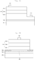
- Fig. 23 is a cross-sectional view illustrating a light emitting chip which is included in a light emitting device package according to the embodiment.
- the light emitting chip includes a substrate 511, a buffer layer 512, a light emitting structure 510, a first electrode 516 and a second electrode 517.
- the substrate 511 may be made of light transparent material or non-light transparent material and may include a conductive substrate or an insulating substrate.
- the buffer layer 512 reduces a lattice constant difference between material of the substrate 512 and material of the light emitting structure 510 and may be made of a nitride semiconductor.
- a nitride semiconductor layer which is not doped with dopant is further formed between the buffer layer 512 and the light emitting structure 510 and thus can improve crystal quality.
- the light emitting structure 510 include a first conductive semiconductor layer 513, an active layer 514, and a second conductive semiconductor layer 515.
- the first conductive semiconductor layer 513 may be formed in a single layer or multi-layers.
- the first conductive semiconductor layer 513 may be doped with a first conductive dopant.
- the first conductive semiconductor layer 513 in a case where the first conductive semiconductor layer 513 is an n-type semiconductor layer, it may include a n-type dopant.
- the n-type dopant may include Si, Ge, Sn, Se, and Te.
- the first conductive semiconductor layer 513 may include a composition formula of In x Al y Ga 1-x-y N (0 ⁇ x ⁇ 1, 0 ⁇ y ⁇ 1, 0 ⁇ x+y ⁇ 1).
- the first conductive semiconductor layer 513 may include a stacked structure of layers including at least one of compound semiconductors such as GaN, InN, AlN, InGaN, AlGaN, InAlGaN, AlInN, AlGaAs, GaP, GaAs, GaAsP, and AlGaInP, for example.
- compound semiconductors such as GaN, InN, AlN, InGaN, AlGaN, InAlGaN, AlInN, AlGaAs, GaP, GaAs, GaAsP, and AlGaInP, for example.
- a first cladding layer may be formed between the first conductive semiconductor layer 513 and the active layer 514.
- the cladding layer may be formed in a GaN-based semiconductor and a band gap of the cladding layer may be equal to or greater than the band gap of the active layer 514.
- This first cladding layer may be a first conductivity type and may include ability to constrain a carrier.
- the active layer 514 is disposed on the first conductive semiconductor layer 513 and may selectively include a single quantum well, multiple quantum wells (MQW), quantum wire structure, or a quantum dot structure.
- the active layer 514 may include a cycle of well layer and barrier layer.
- the well layer may include a composition formula of In x Al y Ga 1-x-y N (0 ⁇ x ⁇ 1, 0 ⁇ y ⁇ 1, 0 ⁇ x+y ⁇ 1) and the barrier layer may include a composition formula of In x Al y Ga 1-x-y N (0 ⁇ x ⁇ 1, 0 ⁇ y ⁇ 1, 0 ⁇ x+y ⁇ 1).
- the cycle of the well layer and the barrier layer may be formed in at least one cycle using stacked structures of InGaN/GaN, GaN/AlGaN, InGaN/AlGaN, InGaN/InGaN, and InAlGaN/InAlGaN, for example.
- the barrier layer may be formed in semiconductor material having a band gap which is higher than a band gap of the well layer.
- the second conductive semiconductor layer 515 is formed on the active layer 514.
- the second conductive semiconductor layer 515 may be implemented with compound semiconductors, such as compound semiconductors of group II - group IV and group III-group V.
- the second conductive semiconductor layer 515 may be formed in a single layer or multi-layers.
- the second conductive dopant may include Mg, Zn, Ca, Sr, Ba, or the like, as a p-type dopant.
- the second conductive semiconductor layer 515 may be doped with a second conductive dopant.
- the second conductive semiconductor layer 515 may include a composition formula of In x Al y Ga 1-x-y N (0 ⁇ x ⁇ 1, 0 ⁇ y ⁇ 1, 0 ⁇ x+y ⁇ 1).
- the second conductive semiconductor layer 515 may be made of any one of compound semiconductors such as GaN, InN, AlN, InGaN, AlGaN, InAlGaN, AlInN, AlGaAs, GaP, GaAs, GaAsP, and AlGaInP, for example.
- the second conductive semiconductor layer 515 may include a super-lattice structure and the super-lattice structure may include an InGaN/GaN super-lattice structure or an AlGaN/GaN super-lattice structure.
- the super-lattice structure of the second conductive semiconductor layer 515 may protect the active layer 514 by diffusing a current which is abnormally included in voltage.
- the first conductive semiconductor layer 513 is described as a n-type semiconductor layer and the second conductive semiconductor layer 515 is described as a p-type semiconductor layer, the first conductive semiconductor layer 513 is described as a p-type semiconductor layer and the second conductive semiconductor layer 515 is described as a n-type semiconductor layer.
- a semiconductor having a polarity opposite to the polarity of the second conductivity type for example n-type semiconductor layer (not illustrated) may be formed on the second conductive semiconductor layer 515.
- the light emitting structure 510 may be implemented as any one structure among an n-p junction structure, a p-n junction structure, a n-p-n junction structure, and a p-n-p junction structure.
- a first electrode 516 is disposed on the first conductive semiconductor layer 513 and a second electrode 517 having a current diffusion layer is included on the second conductive semiconductor layer 513.
- Fig. 24 is a cross-sectional view illustrating another example of a light emitting chip which is included in a light emitting device package according to an embodiment.
- a light emitting chip of another example refers to Fig. 6 . Therefore, description of the same configuration will be omitted.
- a contacting layer 521 may be disposed under the light emitting structure 510
- a reflective layer 524 may be disposed under the contacting layer 521
- a supporting member 525 may be disposed under the reflective layer 524
- a protection layer 523 may be disposed around the light emitting structure 510 and the reflective layer 524.
- the light emitting chip may be disposed the contacting layer 521 and the protection layer 523, the reflective layer 524 and the supporting member 525 under the second conductive semiconductor layer 515.
- the contacting layer 521 may have an ohmic contact with a lower surface of the light emitting structure 510, for example the second conductive semiconductor layer 515.
- the contacting layer 521 may be selected among metal nitride, an insulating material, and a conductive material.
- the contacting layer 521 may be formed among materials consisting of indium tin oxide (ITO), indium zinc oxide (IZO), indium zinc tin oxide (IZTO), indium aluminum zinc oxide (IAZO), indium gallium zinc oxide (IGZO), indium gallium tin oxide (IGTO), aluminum zinc oxide (AZO), antimony tin oxide (ATO), gallium zinc oxide (GZO), Ag, Ni, Al, Rh, Pd, Ir, Ru, Mg, Zn, Pt, Au, Hf and a selective combination thereof.
- ITO indium tin oxide
- IZO indium zinc oxide
- IZTO indium aluminum zinc oxide
- IAZO indium gallium zinc oxide
- IGZO indium gallium zinc oxide
- IGTO aluminum zinc oxide
- ATO antimony tin oxide
- GaZO gallium zinc oxide
- Ag Ni, Al, Rh, Pd, Ir, Ru, Mg, Zn, Pt, Au, Hf and a selective combination thereof.
- the contacting layer may be formed in the multilayer using metal material and light transmissive and conductive material such as IZO, IZTO, IAZO, IGZO, IGTO, AZO, ATO and may be stacked with IZO/Ni, AZO/Ag, IZO/Ag/Ni, AZO/Ag/Ni, for example.
- a current blocking layer which blocks current to correspond to the electrode 615 may further formed in the contacting layer 521.
- the protection layer 523 may be selected among metal oxide and an insulating material.
- the protecting layer 523 may be selectively formed among materials consisting of indium tin oxide (ITO), indium zinc oxide (IZO), indium zinc tin oxide (IZTO), indium aluminum zinc oxide (IAZO), indium gallium zinc oxide (IGZO), indium gallium tin oxide (IGTO), aluminum zinc oxide (AZO), antimony tin oxide (ATO), gallium zinc oxide (GZO), SiO 2 , SiO x , SiO x N y , Si 3 N 4 , Al 2 O 3 , and TiO 2 .
- the protection layer 523 may be formed by using a sputtering method, the vapor deposition method, or the like. Metal such as the reflection layer 524 can prevent layers of the light emitting structure 510 to be short-circuited.
- the reflective layer 524 may include metal.
- the reflective layer 524 may be formed in Ag, Ni, Al, Rh, Pd, Ir, Ru, Mg, Zn, Pt, Au, Hf and material consisting of a selective combination thereof.
- the reflective layer 524 is capable of improving light reflection efficiency by the width thereof being formed to be greater than the width of the light emitting structure 510.
- a metal layer for bonding, a metal layer for thermal diffusion may be further disposed between the reflective layer 524 and the supporting member 525. However it is not limited to this.
- the supporting member 525 may be implemented with metal such as Copper (Cu), gold (Au), nickel (Ni), molybdenum (Mo), copper-tungsten (Cu-W) or a carrier wafer (for example: Si, Ge, GaAs, ZnO, SiC) as a base substrate.
- a bonding layer may be further formed between the supporting member 525 and the reflective layer 524.
- Fig. 25 is a perspective view illustrating a display device which includes a light emitting device package according to an embodiment.
- a display apparatus 1000 may include a light guide plate 1041, a light source module 1031 which provide light to the light guide plate 1041, a reflection member 1022 under the light guide plate 1041, an optical sheet 1051 on the light guide plate 1041, a display panel 1061 on the optical sheet 1051, and a bottom cover 1011 which accommodates the light guide plate 1041, the light source module 1031, and the reflection member 1022.
- a light guide plate 1041 a light source module 1031 which provide light to the light guide plate 1041, a reflection member 1022 under the light guide plate 1041, an optical sheet 1051 on the light guide plate 1041, a display panel 1061 on the optical sheet 1051, and a bottom cover 1011 which accommodates the light guide plate 1041, the light source module 1031, and the reflection member 1022.
- a bottom cover 1011 which accommodates the light guide plate 1041, the light source module 1031, and the reflection member 1022.
- the bottom cover 1011, the reflection member 1022, the light guide plate 1041, and the optical sheet 1051 may be defined as a light unit 1050.
- the light guide plate 1041 serves to diffuse the light and thus to be a surface light source.
- the light guide plate 1041 may be made of transparent material and may include one of acrylic resin based material such as polymethyl metaacrylate (PMMA) and resin such as polyethylene terephthlate (PET), poly carbonate (PC), cycloolefin copolymer (COC) and polyethylene naphthalate (PEN).
- PMMA polymethyl metaacrylate
- PET polyethylene terephthlate
- PC poly carbonate
- COC cycloolefin copolymer
- PEN polyethylene naphthalate
- the light source module 1031 provides light on at least one side surface of the light guide plate 1041 and ultimately acts as a light source of the display device.
- At least one light source module 1031 may be provided and may directly or indirectly provide light from a side surface of the light guide plate 1041.
- the optical module 1031 include a substrate 1033 and the light emitting device package 110 according to the embodiment and a plurality of light emitting device packages 110 may be disposed on the substrate 1033 in a state of being spaced apart from each other by a fixed distance.
- the substrate 1033 may be a printed circuit board (PCB) including a circuit pattern (not illustrated).
- the substrate 1033 may includes a general PCB as well as a metal core PCB (MCPCB), a flexible PCB (FPCB), or the like.
- MCPCB metal core PCB
- FPCB flexible PCB
- the light emitting device package 110 may be directly disposed on a side surface of the bottom cover 1011 or a heat dissipation plate.
- the reflection member 1022 may be disposed under the light guide plate 1041.
- the reflection member 1022 is capable of improving the brightness of the light unit 1050 by reflecting light which is incident on a lower surface of the light guide plate 1041.
- the reflection member 1022 may be made of PET, PC, PVC resin, or the like, for example. However, it is not limited to this.
- the bottom cover 1011 may accommodates the light guide plate 1041, the light source module 1031, the reflection member 1022, or the like.
- the bottom cover 1011 may include an accommodating portion 1012 having a box shape of which an upper surface is opened. However, it is not limited to this.
- the bottom cover 1011 may couple with a top cover. However, it is not limited to this.
- the bottom cover 1011 may be made of metal material or resin material and may be manufactured using a process such as press molding, extrusion molding.
- the bottom cover 1011 may include metallic or non-metallic materials having good thermal conductivity. However, it is not limited to this.
- the display panel 1061 may include a first substrate and a second substrate which are transparent and face each other, and a liquid crystal layer which is inserted between the first substrate and the second substrate.
- a polarizing plate may be disposed on at least one surface of the display panel 1061.
- the display panel 1061 displays information by light passed through the optical sheet 1051.
- the display device 1000 can be applied to various types of portable terminals, a monitor of a notebook computer, a monitor of a laptop computer, a television, or the like.
- the optical sheet 1051 may be disposed between the display panel 1061 and the light guide plate 1041.
- the optical sheet 1051 may include at least one transparent sheet.
- the optical sheet 1051 may include at least one among a diffusion sheet, at least one of prism sheet, and the protection sheet.
- the diffusion sheet may include a function which diffuses light which is incident.
- the diffusion sheet may include a function which condenses light which is incident into a display area.
- the protection sheet may include a function which protects the prism sheet.
- Fig. 26 is a cross-sectional view illustrating another example of a display device which includes a light emitting device package according to an embodiment.
- a display device 1100 of another example may include a bottom cover 1152, a substrate 1120 on which the light emitting device package 110 is mounted, an optical member 1154, and a display panel 1155.
- the substrate 1120 and the light emitting device package 110 may be defined as a light source module 1160.
- the bottom cover 1152, at least one light source module 1160, and an optical member 1154 may be defined as a light unit 1150.
- the bottom cover 1152 may include an accommodating portion 1153.
- the light source module 1160 may include a substrate 1120 and a plurality of light emitting device package 110 which is disposed on the substrate 1120.
- the optical member 1154 may include at least one of lens, a diffusion plate, a diffusion sheet, a prism sheet, and a protective sheet.
- the diffusion plate may be made of PC material or poly methyl methacrylate (PMMA) material and the diffusion plate may be removed.
- PMMA poly methyl methacrylate
- the diffusion sheet may diffuse incident light
- the prism sheet may condense the incident light into a display area
- the protection sheet may protect the prism sheet.
- the optical member 1154 is disposed on the light source module 1060, is to be surface light source using light emitted from the light source module 1060 and performs diffusion, condensation, or the like of the light emitted from the light source module 1060.
- the light emitting device package 110 may be applied to the display device as well as lighting units, indication units, lamps, street lights, vehicle lighting devices, vehicle display devices, smart watches, or the like. However, it is not limited to this.
Landscapes
- Led Device Packages (AREA)
Applications Claiming Priority (2)
| Application Number | Priority Date | Filing Date | Title |
|---|---|---|---|
| KR20150143629 | 2015-10-14 | ||
| KR1020160122480A KR101831249B1 (ko) | 2015-10-14 | 2016-09-23 | 발광소자 패키지 및 조명 장치 |
Publications (2)
| Publication Number | Publication Date |
|---|---|
| EP3157058A1 EP3157058A1 (en) | 2017-04-19 |
| EP3157058B1 true EP3157058B1 (en) | 2020-02-26 |
Family
ID=57136787
Family Applications (1)
| Application Number | Title | Priority Date | Filing Date |
|---|---|---|---|
| EP16193981.4A Active EP3157058B1 (en) | 2015-10-14 | 2016-10-14 | Light emitting device package and lighting apparatus having same |
Country Status (3)
| Country | Link |
|---|---|
| US (4) | US9793457B2 (enExample) |
| EP (1) | EP3157058B1 (enExample) |
| JP (1) | JP6862141B2 (enExample) |
Families Citing this family (11)
| Publication number | Priority date | Publication date | Assignee | Title |
|---|---|---|---|---|
| JP6508131B2 (ja) * | 2016-05-31 | 2019-05-08 | 日亜化学工業株式会社 | 発光装置 |
| WO2018233840A1 (en) * | 2017-06-22 | 2018-12-27 | Osram Opto Semiconductors Gmbh | OPTOELECTRONIC COMPONENT |
| JP2019033209A (ja) * | 2017-08-09 | 2019-02-28 | シチズン時計株式会社 | 発光ダイオード |
| KR102385940B1 (ko) | 2017-09-01 | 2022-04-13 | 쑤저우 레킨 세미컨덕터 컴퍼니 리미티드 | 발광소자 패키지 및 광원 장치 |
| JP7001814B2 (ja) * | 2017-09-08 | 2022-01-20 | オスラム オプト セミコンダクターズ ゲゼルシャフト ミット ベシュレンクテル ハフツング | 発光部品および発光部品を製造するための方法 |
| JP6793139B2 (ja) * | 2018-01-25 | 2020-12-02 | 日機装株式会社 | 半導体発光装置 |
| US11309349B2 (en) | 2018-08-21 | 2022-04-19 | Hewlett-Packard Development Company, L.P. | P-type semiconductor layers coupled to N-type semiconductor layers |
| KR102861696B1 (ko) * | 2018-09-07 | 2025-09-18 | 서울반도체 주식회사 | 발광 다이오드 패키지 |
| JP7337590B2 (ja) * | 2019-08-05 | 2023-09-04 | ローム株式会社 | 半導体発光装置 |
| JP7295437B2 (ja) * | 2019-11-29 | 2023-06-21 | 日亜化学工業株式会社 | 発光装置 |
| DE102022112609A1 (de) * | 2022-05-19 | 2023-11-23 | Ams-Osram International Gmbh | Gehäuse und leiterrahmeneinheit |
Family Cites Families (35)
| Publication number | Priority date | Publication date | Assignee | Title |
|---|---|---|---|---|
| US6808316B2 (en) * | 2001-06-29 | 2004-10-26 | Sumitomo Electric Industries, Ltd. | Optical communication module |
| ITTO20040117A1 (it) | 2004-02-27 | 2004-05-27 | Tek Srl | Kit per il gonfiaggio e la riparazione di articoli gonfiabili, in particolare pneumatici |
| KR100604408B1 (ko) | 2005-08-26 | 2006-07-25 | 삼성전기주식회사 | 발광 다이오드 패키지 |
| JP4789673B2 (ja) * | 2005-10-27 | 2011-10-12 | 京セラ株式会社 | 発光素子収納用パッケージならびにこれを用いた光源および発光装置 |
| JP5168152B2 (ja) | 2006-12-28 | 2013-03-21 | 日亜化学工業株式会社 | 発光装置 |
| KR100901618B1 (ko) * | 2007-04-19 | 2009-06-08 | 엘지이노텍 주식회사 | 발광 다이오드 패키지 및 제조방법 |
| KR20090002284A (ko) * | 2007-06-26 | 2009-01-09 | 엘지이노텍 주식회사 | 발광 장치 |
| JP5395382B2 (ja) | 2007-08-07 | 2014-01-22 | 株式会社半導体エネルギー研究所 | トランジスタの作製方法 |
| JP2009295892A (ja) | 2008-06-09 | 2009-12-17 | Nichia Corp | 発光装置 |
| KR101007131B1 (ko) | 2008-11-25 | 2011-01-10 | 엘지이노텍 주식회사 | 발광 소자 패키지 |
| JP5280818B2 (ja) | 2008-11-28 | 2013-09-04 | シャープ株式会社 | 発光装置 |
| KR101064072B1 (ko) * | 2009-02-24 | 2011-09-08 | 엘지이노텍 주식회사 | 발광 소자 패키지 |
| JP2011023557A (ja) | 2009-07-16 | 2011-02-03 | Toshiba Corp | 発光装置 |
| JP5810302B2 (ja) * | 2010-06-28 | 2015-11-11 | パナソニックIpマネジメント株式会社 | 発光装置、バックライトユニット、液晶表示装置及び照明装置 |
| KR101114197B1 (ko) * | 2010-08-09 | 2012-02-22 | 엘지이노텍 주식회사 | 발광 소자 및 이를 구비한 조명 시스템 |
| WO2012036281A1 (ja) * | 2010-09-17 | 2012-03-22 | ローム株式会社 | 半導体発光装置、その製造方法、および表示装置 |
| JP5886584B2 (ja) * | 2010-11-05 | 2016-03-16 | ローム株式会社 | 半導体発光装置 |
| CN102130273A (zh) | 2010-12-10 | 2011-07-20 | 深圳市华星光电技术有限公司 | 发光二极管封装构造 |
| KR101788723B1 (ko) * | 2011-04-28 | 2017-10-20 | 엘지이노텍 주식회사 | 발광 소자 패키지 |
| TWM419231U (en) * | 2011-07-01 | 2011-12-21 | Lextar Electronics Corp | Light emitting diode package structure |
| KR101831274B1 (ko) | 2011-07-07 | 2018-02-22 | 엘지이노텍 주식회사 | 발광소자 패키지 및 전자기기. |
| KR101884628B1 (ko) * | 2011-08-24 | 2018-08-02 | 엘지이노텍 주식회사 | 발광 모듈 및 백라이트 유닛 |
| KR101923688B1 (ko) | 2011-08-29 | 2018-11-29 | 엘지이노텍 주식회사 | 발광소자 패키지 및 라이트 유닛 |
| KR101905535B1 (ko) | 2011-11-16 | 2018-10-10 | 엘지이노텍 주식회사 | 발광 소자 패키지 및 이를 구비한 조명 장치 |
| CN202474018U (zh) * | 2011-12-23 | 2012-10-03 | 深圳市瑞丰光电子股份有限公司 | Led封装结构 |
| KR101979942B1 (ko) * | 2012-01-03 | 2019-05-17 | 엘지이노텍 주식회사 | 발광 소자 패키지 및 이를 구비한 조명 시스템 |
| KR20130098048A (ko) | 2012-02-27 | 2013-09-04 | 엘지이노텍 주식회사 | 발광소자 패키지 |
| US20140021491A1 (en) * | 2012-07-18 | 2014-01-23 | Carsem (M) Sdn. Bhd. | Multi-compound molding |
| KR102042150B1 (ko) * | 2012-09-13 | 2019-11-07 | 엘지이노텍 주식회사 | 발광 소자 및 조명 시스템 |
| KR102033928B1 (ko) | 2012-09-13 | 2019-10-18 | 엘지이노텍 주식회사 | 발광 소자 및 조명 시스템 |
| KR102053287B1 (ko) * | 2013-04-29 | 2019-12-06 | 엘지이노텍 주식회사 | 발광 소자 및 이를 구비한 조명 시스템 |
| TW201513402A (zh) * | 2013-09-27 | 2015-04-01 | Lextar Electronics Corp | 發光二極體封裝結構 |
| JP6176101B2 (ja) * | 2013-12-17 | 2017-08-09 | 日亜化学工業株式会社 | 樹脂パッケージ及び発光装置 |
| JP2015179777A (ja) | 2014-03-19 | 2015-10-08 | 株式会社東芝 | 半導体発光装置 |
| JP6627227B2 (ja) * | 2015-02-27 | 2020-01-08 | 日亜化学工業株式会社 | 発光装置及び発光装置の製造方法 |
-
2016
- 2016-10-12 JP JP2016200889A patent/JP6862141B2/ja not_active Expired - Fee Related
- 2016-10-13 US US15/293,029 patent/US9793457B2/en active Active
- 2016-10-14 EP EP16193981.4A patent/EP3157058B1/en active Active
-
2017
- 2017-09-08 US US15/699,900 patent/US10170676B2/en not_active Ceased
-
2019
- 2019-03-15 US US16/354,981 patent/USRE48892E1/en active Active
- 2019-03-26 US US16/364,363 patent/USRE49146E1/en active Active
Non-Patent Citations (1)
| Title |
|---|
| None * |
Also Published As
| Publication number | Publication date |
|---|---|
| US20170373236A1 (en) | 2017-12-28 |
| US10170676B2 (en) | 2019-01-01 |
| JP6862141B2 (ja) | 2021-04-21 |
| US9793457B2 (en) | 2017-10-17 |
| US20170110637A1 (en) | 2017-04-20 |
| USRE48892E1 (en) | 2022-01-11 |
| JP2017076793A (ja) | 2017-04-20 |
| USRE49146E1 (en) | 2022-07-19 |
| EP3157058A1 (en) | 2017-04-19 |
Similar Documents
| Publication | Publication Date | Title |
|---|---|---|
| EP3157058B1 (en) | Light emitting device package and lighting apparatus having same | |
| KR101997243B1 (ko) | 발광 소자 및 조명 시스템 | |
| US9620693B2 (en) | Light emitting device and lighting system having the same | |
| US9249957B2 (en) | Light emitting device and lighting system including the same | |
| KR102075561B1 (ko) | 발광 소자, 발광 모듈 및 조명 시스템 | |
| KR101831249B1 (ko) | 발광소자 패키지 및 조명 장치 | |
| KR20140088744A (ko) | 광학 렌즈, 이를 구비한 발광 모듈 및 조명 시스템 | |
| KR102528014B1 (ko) | 발광소자 패키지 및 조명 장치 | |
| KR20140028794A (ko) | 발광소자 및 이를 구비한 조명 시스템 | |
| KR101946831B1 (ko) | 발광 소자 패키지 | |
| KR102019498B1 (ko) | 발광 소자 및 조명 시스템 | |
| KR102042271B1 (ko) | 발광 소자 및 조명 시스템 | |
| KR102486034B1 (ko) | 발광소자 패키지 및 조명 장치 | |
| KR101896691B1 (ko) | 발광 소자 및 조명 시스템 | |
| KR101905506B1 (ko) | 발광 소자 패키지 및 이를 구비한 조명 시스템 | |
| KR20140035214A (ko) | 발광 소자 및 조명 시스템 | |
| KR20140046735A (ko) | 발광 소자, 발광 소자 제조방법 및 조명 시스템 | |
| KR20190024930A (ko) | 발광소자 및 이를 구비한 조명 시스템 | |
| KR20170062156A (ko) | 발광소자 패키지 및 조명 장치 | |
| KR20170062168A (ko) | 발광소자 패키지 및 조명 장치 |
Legal Events
| Date | Code | Title | Description |
|---|---|---|---|
| REG | Reference to a national code |
Ref country code: DE Ref legal event code: R138 Ref document number: 202016008784 Country of ref document: DE Free format text: GERMAN DOCUMENT NUMBER IS 602016030461 |
|
| PUAI | Public reference made under article 153(3) epc to a published international application that has entered the european phase |
Free format text: ORIGINAL CODE: 0009012 |
|
| STAA | Information on the status of an ep patent application or granted ep patent |
Free format text: STATUS: REQUEST FOR EXAMINATION WAS MADE |
|
| 17P | Request for examination filed |
Effective date: 20161107 |
|
| AK | Designated contracting states |
Kind code of ref document: A1 Designated state(s): AL AT BE BG CH CY CZ DE DK EE ES FI FR GB GR HR HU IE IS IT LI LT LU LV MC MK MT NL NO PL PT RO RS SE SI SK SM TR |
|
| AX | Request for extension of the european patent |
Extension state: BA ME |
|
| RAP1 | Party data changed (applicant data changed or rights of an application transferred) |
Owner name: LG INNOTEK CO., LTD. |
|
| RBV | Designated contracting states (corrected) |
Designated state(s): AL AT BE BG CH CY CZ DE DK EE ES FI FR GB GR HR HU IE IS IT LI LT LU LV MC MK MT NL NO PL PT RO RS SE SI SK SM TR |
|
| GRAP | Despatch of communication of intention to grant a patent |
Free format text: ORIGINAL CODE: EPIDOSNIGR1 |
|
| STAA | Information on the status of an ep patent application or granted ep patent |
Free format text: STATUS: GRANT OF PATENT IS INTENDED |
|
| RIC1 | Information provided on ipc code assigned before grant |
Ipc: H01L 23/495 20060101ALN20190813BHEP Ipc: H01L 25/16 20060101AFI20190813BHEP Ipc: H01L 33/48 20100101ALN20190813BHEP Ipc: H01L 33/62 20100101ALI20190813BHEP Ipc: H01L 33/60 20100101ALI20190813BHEP Ipc: H01L 25/075 20060101ALI20190813BHEP |
|
| INTG | Intention to grant announced |
Effective date: 20190909 |
|
| GRAS | Grant fee paid |
Free format text: ORIGINAL CODE: EPIDOSNIGR3 |
|
| GRAA | (expected) grant |
Free format text: ORIGINAL CODE: 0009210 |
|
| STAA | Information on the status of an ep patent application or granted ep patent |
Free format text: STATUS: THE PATENT HAS BEEN GRANTED |
|
| AK | Designated contracting states |
Kind code of ref document: B1 Designated state(s): AL AT BE BG CH CY CZ DE DK EE ES FI FR GB GR HR HU IE IS IT LI LT LU LV MC MK MT NL NO PL PT RO RS SE SI SK SM TR |
|
| REG | Reference to a national code |
Ref country code: GB Ref legal event code: FG4D |
|
| REG | Reference to a national code |
Ref country code: CH Ref legal event code: EP |
|
| REG | Reference to a national code |
Ref country code: AT Ref legal event code: REF Ref document number: 1238679 Country of ref document: AT Kind code of ref document: T Effective date: 20200315 |
|
| REG | Reference to a national code |
Ref country code: IE Ref legal event code: FG4D |
|
| REG | Reference to a national code |
Ref country code: DE Ref legal event code: R096 Ref document number: 602016030461 Country of ref document: DE |
|
| PG25 | Lapsed in a contracting state [announced via postgrant information from national office to epo] |
Ref country code: RS Free format text: LAPSE BECAUSE OF FAILURE TO SUBMIT A TRANSLATION OF THE DESCRIPTION OR TO PAY THE FEE WITHIN THE PRESCRIBED TIME-LIMIT Effective date: 20200226 Ref country code: NO Free format text: LAPSE BECAUSE OF FAILURE TO SUBMIT A TRANSLATION OF THE DESCRIPTION OR TO PAY THE FEE WITHIN THE PRESCRIBED TIME-LIMIT Effective date: 20200526 Ref country code: FI Free format text: LAPSE BECAUSE OF FAILURE TO SUBMIT A TRANSLATION OF THE DESCRIPTION OR TO PAY THE FEE WITHIN THE PRESCRIBED TIME-LIMIT Effective date: 20200226 |
|
| REG | Reference to a national code |
Ref country code: NL Ref legal event code: MP Effective date: 20200226 |
|
| REG | Reference to a national code |
Ref country code: LT Ref legal event code: MG4D |
|
| PG25 | Lapsed in a contracting state [announced via postgrant information from national office to epo] |
Ref country code: BG Free format text: LAPSE BECAUSE OF FAILURE TO SUBMIT A TRANSLATION OF THE DESCRIPTION OR TO PAY THE FEE WITHIN THE PRESCRIBED TIME-LIMIT Effective date: 20200526 Ref country code: GR Free format text: LAPSE BECAUSE OF FAILURE TO SUBMIT A TRANSLATION OF THE DESCRIPTION OR TO PAY THE FEE WITHIN THE PRESCRIBED TIME-LIMIT Effective date: 20200527 Ref country code: SE Free format text: LAPSE BECAUSE OF FAILURE TO SUBMIT A TRANSLATION OF THE DESCRIPTION OR TO PAY THE FEE WITHIN THE PRESCRIBED TIME-LIMIT Effective date: 20200226 Ref country code: IS Free format text: LAPSE BECAUSE OF FAILURE TO SUBMIT A TRANSLATION OF THE DESCRIPTION OR TO PAY THE FEE WITHIN THE PRESCRIBED TIME-LIMIT Effective date: 20200626 Ref country code: LV Free format text: LAPSE BECAUSE OF FAILURE TO SUBMIT A TRANSLATION OF THE DESCRIPTION OR TO PAY THE FEE WITHIN THE PRESCRIBED TIME-LIMIT Effective date: 20200226 Ref country code: HR Free format text: LAPSE BECAUSE OF FAILURE TO SUBMIT A TRANSLATION OF THE DESCRIPTION OR TO PAY THE FEE WITHIN THE PRESCRIBED TIME-LIMIT Effective date: 20200226 |
|
| PG25 | Lapsed in a contracting state [announced via postgrant information from national office to epo] |
Ref country code: NL Free format text: LAPSE BECAUSE OF FAILURE TO SUBMIT A TRANSLATION OF THE DESCRIPTION OR TO PAY THE FEE WITHIN THE PRESCRIBED TIME-LIMIT Effective date: 20200226 |
|
| PG25 | Lapsed in a contracting state [announced via postgrant information from national office to epo] |
Ref country code: EE Free format text: LAPSE BECAUSE OF FAILURE TO SUBMIT A TRANSLATION OF THE DESCRIPTION OR TO PAY THE FEE WITHIN THE PRESCRIBED TIME-LIMIT Effective date: 20200226 Ref country code: LT Free format text: LAPSE BECAUSE OF FAILURE TO SUBMIT A TRANSLATION OF THE DESCRIPTION OR TO PAY THE FEE WITHIN THE PRESCRIBED TIME-LIMIT Effective date: 20200226 Ref country code: DK Free format text: LAPSE BECAUSE OF FAILURE TO SUBMIT A TRANSLATION OF THE DESCRIPTION OR TO PAY THE FEE WITHIN THE PRESCRIBED TIME-LIMIT Effective date: 20200226 Ref country code: SM Free format text: LAPSE BECAUSE OF FAILURE TO SUBMIT A TRANSLATION OF THE DESCRIPTION OR TO PAY THE FEE WITHIN THE PRESCRIBED TIME-LIMIT Effective date: 20200226 Ref country code: SK Free format text: LAPSE BECAUSE OF FAILURE TO SUBMIT A TRANSLATION OF THE DESCRIPTION OR TO PAY THE FEE WITHIN THE PRESCRIBED TIME-LIMIT Effective date: 20200226 Ref country code: PT Free format text: LAPSE BECAUSE OF FAILURE TO SUBMIT A TRANSLATION OF THE DESCRIPTION OR TO PAY THE FEE WITHIN THE PRESCRIBED TIME-LIMIT Effective date: 20200719 Ref country code: ES Free format text: LAPSE BECAUSE OF FAILURE TO SUBMIT A TRANSLATION OF THE DESCRIPTION OR TO PAY THE FEE WITHIN THE PRESCRIBED TIME-LIMIT Effective date: 20200226 Ref country code: RO Free format text: LAPSE BECAUSE OF FAILURE TO SUBMIT A TRANSLATION OF THE DESCRIPTION OR TO PAY THE FEE WITHIN THE PRESCRIBED TIME-LIMIT Effective date: 20200226 Ref country code: CZ Free format text: LAPSE BECAUSE OF FAILURE TO SUBMIT A TRANSLATION OF THE DESCRIPTION OR TO PAY THE FEE WITHIN THE PRESCRIBED TIME-LIMIT Effective date: 20200226 |
|
| REG | Reference to a national code |
Ref country code: AT Ref legal event code: MK05 Ref document number: 1238679 Country of ref document: AT Kind code of ref document: T Effective date: 20200226 |
|
| REG | Reference to a national code |
Ref country code: DE Ref legal event code: R097 Ref document number: 602016030461 Country of ref document: DE |
|
| PLBE | No opposition filed within time limit |
Free format text: ORIGINAL CODE: 0009261 |
|
| STAA | Information on the status of an ep patent application or granted ep patent |
Free format text: STATUS: NO OPPOSITION FILED WITHIN TIME LIMIT |
|
| PG25 | Lapsed in a contracting state [announced via postgrant information from national office to epo] |
Ref country code: IT Free format text: LAPSE BECAUSE OF FAILURE TO SUBMIT A TRANSLATION OF THE DESCRIPTION OR TO PAY THE FEE WITHIN THE PRESCRIBED TIME-LIMIT Effective date: 20200226 Ref country code: AT Free format text: LAPSE BECAUSE OF FAILURE TO SUBMIT A TRANSLATION OF THE DESCRIPTION OR TO PAY THE FEE WITHIN THE PRESCRIBED TIME-LIMIT Effective date: 20200226 |
|
| 26N | No opposition filed |
Effective date: 20201127 |
|
| PG25 | Lapsed in a contracting state [announced via postgrant information from national office to epo] |
Ref country code: SI Free format text: LAPSE BECAUSE OF FAILURE TO SUBMIT A TRANSLATION OF THE DESCRIPTION OR TO PAY THE FEE WITHIN THE PRESCRIBED TIME-LIMIT Effective date: 20200226 Ref country code: PL Free format text: LAPSE BECAUSE OF FAILURE TO SUBMIT A TRANSLATION OF THE DESCRIPTION OR TO PAY THE FEE WITHIN THE PRESCRIBED TIME-LIMIT Effective date: 20200226 |
|
| REG | Reference to a national code |
Ref country code: CH Ref legal event code: PL |
|
| GBPC | Gb: european patent ceased through non-payment of renewal fee |
Effective date: 20201014 |
|
| PG25 | Lapsed in a contracting state [announced via postgrant information from national office to epo] |
Ref country code: MC Free format text: LAPSE BECAUSE OF FAILURE TO SUBMIT A TRANSLATION OF THE DESCRIPTION OR TO PAY THE FEE WITHIN THE PRESCRIBED TIME-LIMIT Effective date: 20200226 Ref country code: LU Free format text: LAPSE BECAUSE OF NON-PAYMENT OF DUE FEES Effective date: 20201014 |
|
| REG | Reference to a national code |
Ref country code: BE Ref legal event code: MM Effective date: 20201031 |
|
| PG25 | Lapsed in a contracting state [announced via postgrant information from national office to epo] |
Ref country code: FR Free format text: LAPSE BECAUSE OF NON-PAYMENT OF DUE FEES Effective date: 20201031 |
|
| PG25 | Lapsed in a contracting state [announced via postgrant information from national office to epo] |
Ref country code: LI Free format text: LAPSE BECAUSE OF NON-PAYMENT OF DUE FEES Effective date: 20201031 Ref country code: GB Free format text: LAPSE BECAUSE OF NON-PAYMENT OF DUE FEES Effective date: 20201014 Ref country code: BE Free format text: LAPSE BECAUSE OF NON-PAYMENT OF DUE FEES Effective date: 20201031 Ref country code: CH Free format text: LAPSE BECAUSE OF NON-PAYMENT OF DUE FEES Effective date: 20201031 |
|
| REG | Reference to a national code |
Ref country code: DE Ref legal event code: R081 Ref document number: 602016030461 Country of ref document: DE Owner name: SUZHOU LEKIN SEMICONDUCTOR CO. LTD., TAICANG, CN Free format text: FORMER OWNER: LG INNOTEK CO., LTD., SEOUL, KR |
|
| PG25 | Lapsed in a contracting state [announced via postgrant information from national office to epo] |
Ref country code: IE Free format text: LAPSE BECAUSE OF NON-PAYMENT OF DUE FEES Effective date: 20201014 |
|
| PG25 | Lapsed in a contracting state [announced via postgrant information from national office to epo] |
Ref country code: TR Free format text: LAPSE BECAUSE OF FAILURE TO SUBMIT A TRANSLATION OF THE DESCRIPTION OR TO PAY THE FEE WITHIN THE PRESCRIBED TIME-LIMIT Effective date: 20200226 Ref country code: MT Free format text: LAPSE BECAUSE OF FAILURE TO SUBMIT A TRANSLATION OF THE DESCRIPTION OR TO PAY THE FEE WITHIN THE PRESCRIBED TIME-LIMIT Effective date: 20200226 Ref country code: CY Free format text: LAPSE BECAUSE OF FAILURE TO SUBMIT A TRANSLATION OF THE DESCRIPTION OR TO PAY THE FEE WITHIN THE PRESCRIBED TIME-LIMIT Effective date: 20200226 |
|
| PG25 | Lapsed in a contracting state [announced via postgrant information from national office to epo] |
Ref country code: MK Free format text: LAPSE BECAUSE OF FAILURE TO SUBMIT A TRANSLATION OF THE DESCRIPTION OR TO PAY THE FEE WITHIN THE PRESCRIBED TIME-LIMIT Effective date: 20200226 Ref country code: AL Free format text: LAPSE BECAUSE OF FAILURE TO SUBMIT A TRANSLATION OF THE DESCRIPTION OR TO PAY THE FEE WITHIN THE PRESCRIBED TIME-LIMIT Effective date: 20200226 |
|
| PGFP | Annual fee paid to national office [announced via postgrant information from national office to epo] |
Ref country code: DE Payment date: 20230906 Year of fee payment: 8 |
|
| REG | Reference to a national code |
Ref country code: DE Ref legal event code: R119 Ref document number: 602016030461 Country of ref document: DE |
|
| PG25 | Lapsed in a contracting state [announced via postgrant information from national office to epo] |
Ref country code: DE Free format text: LAPSE BECAUSE OF NON-PAYMENT OF DUE FEES Effective date: 20250501 |