EP3143640B1 - Substrate and method of forming the same - Google Patents
Substrate and method of forming the same Download PDFInfo
- Publication number
- EP3143640B1 EP3143640B1 EP15722828.9A EP15722828A EP3143640B1 EP 3143640 B1 EP3143640 B1 EP 3143640B1 EP 15722828 A EP15722828 A EP 15722828A EP 3143640 B1 EP3143640 B1 EP 3143640B1
- Authority
- EP
- European Patent Office
- Prior art keywords
- dielectric layer
- photoactive
- traces
- trace
- insulating dielectric
- Prior art date
- Legal status (The legal status is an assumption and is not a legal conclusion. Google has not performed a legal analysis and makes no representation as to the accuracy of the status listed.)
- Active
Links
- 238000000034 method Methods 0.000 title claims description 55
- 239000000758 substrate Substances 0.000 title claims description 20
- 239000010949 copper Substances 0.000 claims description 24
- RYGMFSIKBFXOCR-UHFFFAOYSA-N Copper Chemical compound [Cu] RYGMFSIKBFXOCR-UHFFFAOYSA-N 0.000 claims description 23
- 229910052802 copper Inorganic materials 0.000 claims description 23
- 239000004065 semiconductor Substances 0.000 claims description 19
- 239000011162 core material Substances 0.000 claims description 14
- 238000007747 plating Methods 0.000 claims description 10
- 239000000203 mixture Substances 0.000 claims description 4
- 238000010030 laminating Methods 0.000 claims description 3
- 238000004519 manufacturing process Methods 0.000 claims description 3
- 229910000679 solder Inorganic materials 0.000 claims description 3
- 230000008569 process Effects 0.000 description 13
- 239000000463 material Substances 0.000 description 9
- 230000008901 benefit Effects 0.000 description 8
- 230000015572 biosynthetic process Effects 0.000 description 6
- 230000001419 dependent effect Effects 0.000 description 5
- 238000005530 etching Methods 0.000 description 5
- VYPSYNLAJGMNEJ-UHFFFAOYSA-N Silicium dioxide Chemical compound O=[Si]=O VYPSYNLAJGMNEJ-UHFFFAOYSA-N 0.000 description 4
- XUIMIQQOPSSXEZ-UHFFFAOYSA-N Silicon Chemical compound [Si] XUIMIQQOPSSXEZ-UHFFFAOYSA-N 0.000 description 4
- 229910052710 silicon Inorganic materials 0.000 description 4
- 239000010703 silicon Substances 0.000 description 4
- 230000009471 action Effects 0.000 description 3
- 239000004020 conductor Substances 0.000 description 3
- 230000008878 coupling Effects 0.000 description 3
- 238000010168 coupling process Methods 0.000 description 3
- 238000005859 coupling reaction Methods 0.000 description 3
- 239000007788 liquid Substances 0.000 description 3
- 238000010297 mechanical methods and process Methods 0.000 description 3
- 230000005226 mechanical processes and functions Effects 0.000 description 3
- 239000002184 metal Substances 0.000 description 3
- 229910052751 metal Inorganic materials 0.000 description 3
- 239000004593 Epoxy Substances 0.000 description 2
- 239000000654 additive Substances 0.000 description 2
- 238000013459 approach Methods 0.000 description 2
- 238000001311 chemical methods and process Methods 0.000 description 2
- 238000004891 communication Methods 0.000 description 2
- 238000007796 conventional method Methods 0.000 description 2
- 238000012986 modification Methods 0.000 description 2
- 230000004048 modification Effects 0.000 description 2
- 230000003287 optical effect Effects 0.000 description 2
- 239000002245 particle Substances 0.000 description 2
- 238000000059 patterning Methods 0.000 description 2
- 238000000926 separation method Methods 0.000 description 2
- 239000000377 silicon dioxide Substances 0.000 description 2
- 239000000126 substance Substances 0.000 description 2
- 238000002679 ablation Methods 0.000 description 1
- 230000001413 cellular effect Effects 0.000 description 1
- 238000011161 development Methods 0.000 description 1
- 238000005553 drilling Methods 0.000 description 1
- 230000009977 dual effect Effects 0.000 description 1
- 238000009713 electroplating Methods 0.000 description 1
- 238000005516 engineering process Methods 0.000 description 1
- 230000006870 function Effects 0.000 description 1
- 239000011521 glass Substances 0.000 description 1
- 230000006872 improvement Effects 0.000 description 1
- 238000009413 insulation Methods 0.000 description 1
- 238000003475 lamination Methods 0.000 description 1
- 150000002739 metals Chemical class 0.000 description 1
- 238000010295 mobile communication Methods 0.000 description 1
- 238000004806 packaging method and process Methods 0.000 description 1
- 238000007788 roughening Methods 0.000 description 1
- 238000000638 solvent extraction Methods 0.000 description 1
- 230000005236 sound signal Effects 0.000 description 1
Images

Classifications
-
- H—ELECTRICITY
- H01—ELECTRIC ELEMENTS
- H01L—SEMICONDUCTOR DEVICES NOT COVERED BY CLASS H10
- H01L23/00—Details of semiconductor or other solid state devices
- H01L23/52—Arrangements for conducting electric current within the device in operation from one component to another, i.e. interconnections, e.g. wires, lead frames
- H01L23/522—Arrangements for conducting electric current within the device in operation from one component to another, i.e. interconnections, e.g. wires, lead frames including external interconnections consisting of a multilayer structure of conductive and insulating layers inseparably formed on the semiconductor body
- H01L23/5226—Via connections in a multilevel interconnection structure
-
- H—ELECTRICITY
- H01—ELECTRIC ELEMENTS
- H01L—SEMICONDUCTOR DEVICES NOT COVERED BY CLASS H10
- H01L21/00—Processes or apparatus adapted for the manufacture or treatment of semiconductor or solid state devices or of parts thereof
- H01L21/02—Manufacture or treatment of semiconductor devices or of parts thereof
- H01L21/04—Manufacture or treatment of semiconductor devices or of parts thereof the devices having potential barriers, e.g. a PN junction, depletion layer or carrier concentration layer
- H01L21/48—Manufacture or treatment of parts, e.g. containers, prior to assembly of the devices, using processes not provided for in a single one of the subgroups H01L21/06 - H01L21/326
- H01L21/4814—Conductive parts
- H01L21/4846—Leads on or in insulating or insulated substrates, e.g. metallisation
- H01L21/4857—Multilayer substrates
-
- H—ELECTRICITY
- H01—ELECTRIC ELEMENTS
- H01L—SEMICONDUCTOR DEVICES NOT COVERED BY CLASS H10
- H01L21/00—Processes or apparatus adapted for the manufacture or treatment of semiconductor or solid state devices or of parts thereof
- H01L21/67—Apparatus specially adapted for handling semiconductor or electric solid state devices during manufacture or treatment thereof; Apparatus specially adapted for handling wafers during manufacture or treatment of semiconductor or electric solid state devices or components ; Apparatus not specifically provided for elsewhere
- H01L21/683—Apparatus specially adapted for handling semiconductor or electric solid state devices during manufacture or treatment thereof; Apparatus specially adapted for handling wafers during manufacture or treatment of semiconductor or electric solid state devices or components ; Apparatus not specifically provided for elsewhere for supporting or gripping
- H01L21/6835—Apparatus specially adapted for handling semiconductor or electric solid state devices during manufacture or treatment thereof; Apparatus specially adapted for handling wafers during manufacture or treatment of semiconductor or electric solid state devices or components ; Apparatus not specifically provided for elsewhere for supporting or gripping using temporarily an auxiliary support
-
- H—ELECTRICITY
- H01—ELECTRIC ELEMENTS
- H01L—SEMICONDUCTOR DEVICES NOT COVERED BY CLASS H10
- H01L21/00—Processes or apparatus adapted for the manufacture or treatment of semiconductor or solid state devices or of parts thereof
- H01L21/70—Manufacture or treatment of devices consisting of a plurality of solid state components formed in or on a common substrate or of parts thereof; Manufacture of integrated circuit devices or of parts thereof
- H01L21/71—Manufacture of specific parts of devices defined in group H01L21/70
- H01L21/768—Applying interconnections to be used for carrying current between separate components within a device comprising conductors and dielectrics
- H01L21/76838—Applying interconnections to be used for carrying current between separate components within a device comprising conductors and dielectrics characterised by the formation and the after-treatment of the conductors
- H01L21/76877—Filling of holes, grooves or trenches, e.g. vias, with conductive material
-
- H—ELECTRICITY
- H01—ELECTRIC ELEMENTS
- H01L—SEMICONDUCTOR DEVICES NOT COVERED BY CLASS H10
- H01L21/00—Processes or apparatus adapted for the manufacture or treatment of semiconductor or solid state devices or of parts thereof
- H01L21/70—Manufacture or treatment of devices consisting of a plurality of solid state components formed in or on a common substrate or of parts thereof; Manufacture of integrated circuit devices or of parts thereof
- H01L21/71—Manufacture of specific parts of devices defined in group H01L21/70
- H01L21/768—Applying interconnections to be used for carrying current between separate components within a device comprising conductors and dielectrics
- H01L21/76838—Applying interconnections to be used for carrying current between separate components within a device comprising conductors and dielectrics characterised by the formation and the after-treatment of the conductors
- H01L21/76895—Local interconnects; Local pads, as exemplified by patent document EP0896365
-
- H—ELECTRICITY
- H01—ELECTRIC ELEMENTS
- H01L—SEMICONDUCTOR DEVICES NOT COVERED BY CLASS H10
- H01L23/00—Details of semiconductor or other solid state devices
- H01L23/52—Arrangements for conducting electric current within the device in operation from one component to another, i.e. interconnections, e.g. wires, lead frames
- H01L23/538—Arrangements for conducting electric current within the device in operation from one component to another, i.e. interconnections, e.g. wires, lead frames the interconnection structure between a plurality of semiconductor chips being formed on, or in, insulating substrates
- H01L23/5383—Multilayer substrates
-
- H—ELECTRICITY
- H01—ELECTRIC ELEMENTS
- H01L—SEMICONDUCTOR DEVICES NOT COVERED BY CLASS H10
- H01L21/00—Processes or apparatus adapted for the manufacture or treatment of semiconductor or solid state devices or of parts thereof
- H01L21/02—Manufacture or treatment of semiconductor devices or of parts thereof
- H01L21/04—Manufacture or treatment of semiconductor devices or of parts thereof the devices having potential barriers, e.g. a PN junction, depletion layer or carrier concentration layer
- H01L21/48—Manufacture or treatment of parts, e.g. containers, prior to assembly of the devices, using processes not provided for in a single one of the subgroups H01L21/06 - H01L21/326
- H01L21/4814—Conductive parts
- H01L21/4846—Leads on or in insulating or insulated substrates, e.g. metallisation
- H01L21/486—Via connections through the substrate with or without pins
-
- H—ELECTRICITY
- H01—ELECTRIC ELEMENTS
- H01L—SEMICONDUCTOR DEVICES NOT COVERED BY CLASS H10
- H01L2221/00—Processes or apparatus adapted for the manufacture or treatment of semiconductor or solid state devices or of parts thereof covered by H01L21/00
- H01L2221/67—Apparatus for handling semiconductor or electric solid state devices during manufacture or treatment thereof; Apparatus for handling wafers during manufacture or treatment of semiconductor or electric solid state devices or components; Apparatus not specifically provided for elsewhere
- H01L2221/683—Apparatus for handling semiconductor or electric solid state devices during manufacture or treatment thereof; Apparatus for handling wafers during manufacture or treatment of semiconductor or electric solid state devices or components; Apparatus not specifically provided for elsewhere for supporting or gripping
- H01L2221/68304—Apparatus for handling semiconductor or electric solid state devices during manufacture or treatment thereof; Apparatus for handling wafers during manufacture or treatment of semiconductor or electric solid state devices or components; Apparatus not specifically provided for elsewhere for supporting or gripping using temporarily an auxiliary support
- H01L2221/68345—Apparatus for handling semiconductor or electric solid state devices during manufacture or treatment thereof; Apparatus for handling wafers during manufacture or treatment of semiconductor or electric solid state devices or components; Apparatus not specifically provided for elsewhere for supporting or gripping using temporarily an auxiliary support used as a support during the manufacture of self supporting substrates
-
- H—ELECTRICITY
- H01—ELECTRIC ELEMENTS
- H01L—SEMICONDUCTOR DEVICES NOT COVERED BY CLASS H10
- H01L23/00—Details of semiconductor or other solid state devices
- H01L23/52—Arrangements for conducting electric current within the device in operation from one component to another, i.e. interconnections, e.g. wires, lead frames
- H01L23/538—Arrangements for conducting electric current within the device in operation from one component to another, i.e. interconnections, e.g. wires, lead frames the interconnection structure between a plurality of semiconductor chips being formed on, or in, insulating substrates
- H01L23/5384—Conductive vias through the substrate with or without pins, e.g. buried coaxial conductors
-
- H—ELECTRICITY
- H01—ELECTRIC ELEMENTS
- H01L—SEMICONDUCTOR DEVICES NOT COVERED BY CLASS H10
- H01L2924/00—Indexing scheme for arrangements or methods for connecting or disconnecting semiconductor or solid-state bodies as covered by H01L24/00
- H01L2924/0001—Technical content checked by a classifier
- H01L2924/0002—Not covered by any one of groups H01L24/00, H01L24/00 and H01L2224/00
Definitions
- This disclosure relates generally to semiconductors, and more specifically, but not exclusively, to methods for formation of semiconductor package substrates.
- semiconductor packaging is formed through layer by layer buildup on a central glass reinforced core material, as one option, to enable fine routing and act as a space transformer between the silicon and motherboard.
- This approach may not provide sufficient routing density especially in cases where die split and very fine routing between both die are needed.
- semiconductor packages can be formed through a coreless process in which the first layer is embedded, this will afford finer routing as it eliminates the need for seed layer removal (improve on compensation).
- These 2 approaches formed through organic substrates are generally trying to compete with silicon interposers and organic interposers that make use of "fab-like" processes - using seed layer sputter, thin liquid resist and forming thin copper routing layer. This provides very fine routing but the cost and the Cu thickness, and consequently electrical resistivity are major drawbacks. Accordingly, there are long-felt industry needs for methods that improve upon conventional methods including the improved methods and apparatus provided hereby.
- US 2010/0139964 describes a printed circuit board, including an upper circuit layer and connection pads of conductive metal buried in an insulation layer.
- Some exemplary embodiments of the disclosure are directed to systems, apparatus, and methods for forming a coreless substrate structure having first and second dielectric layers with very fine embedded traces in the first dielectric layer and a landing/capture padless via extending between both first and second dielectric layers.
- the system, apparatus, and method includes forming a core; laminating a top of the core with a photoactive (photoimageable) dielectric layer; forming a plurality of trace patterns in the photoactive dielectric layer; plating the plurality of trace patterns to form a plurality of traces; forming an insulating dielectric layer on the photoactive dielectric layer; forming a via through the insulating dielectric layer and the photoactive dielectric layer; forming additional routing patterns on the insulating dielectric layer; removing the core; and adding a solder mask.
- the system, apparatus and method includes a semiconductor structure with a coreless substrate having a permanent photoactive dielectric layer and an insulating dielectric layer, a plurality of traces embedded in the permanent photoactive dielectric layer, and means for conducting extending through the insulating dielectric layer and the permanent photoimageable dielectric layer.
- Systems, apparatus, and methods for formation of a coreless substrate with a photoactive (photoimageable) dielectric, padless skip via and embedded traces are provided.
- the exemplary methods disclosed herein advantageously address the long-felt industry needs, as well as other previously unidentified needs, and mitigate shortcomings of the conventional methods.
- advantages provided by the disclosed embodiments herein are an improvement in cost savings, easier manufacturing, lower height profile, via in a bump pad with smaller profile over conventional devices.
- connection means any connection or coupling, either direct or indirect, between elements, and can encompass a presence of an intermediate element between two elements that are “connected” or “coupled” together via the intermediate element. Coupling and/or connection between the elements can be physical, logical, or a combination thereof.
- elements can be “connected” or “coupled” together, for example, by using one or more wires, cables, and/or printed electrical connections, as well as by using electromagnetic energy.
- the electromagnetic energy can have wavelengths in the radio frequency region, the microwave region and/or the optical (both visible and invisible) region.
- signal can include any signal such as a data signal, audio signal, video signal, multimedia signal, analog signal, and/or digital signal.
- Information and signals can be represented using any of a variety of different technologies and techniques. For example, data, an instruction, a process step, a command, information, a signal, a bit, and/or a symbol described in this description can be represented by a voltage, a current, an electromagnetic wave, a magnetic field and/or particle, an optical field and/or particle, and any combination thereof.
- any reference herein to an element using a designation such as “first,” “second,” and so forth does not limit the quantity and/or order of those elements. Rather, these designations are used as a convenient method of distinguishing between two or more elements and/or instances of an element. Thus, a reference to first and second elements does not mean that only two elements can be employed, or that the first element must necessarily precede the second element. Also, unless stated otherwise, a set of elements can comprise one or more elements. In addition, terminology of the form “at least one of: A, B, or C" used in the description or the claims can be interpreted as "A or B or C or any combination of these elements.”
- mobile device can describe, and is not limited to, a mobile phone, a mobile communication device, a pager, a personal digital assistant, a personal information manager, a mobile hand-held computer, a laptop computer, a wireless device, a wireless modem, and/or other types of portable electronic devices typically carried by a person and/or having communication capabilities (e.g., wireless, cellular, infrared, short-range radio, etc.).
- UE user equipment
- mobile terminal mobile terminal
- wireless device wireless device
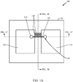
- Fig. 1A depicts an exemplary embodiment of a semiconductor package including a coreless substrate with padless vias and a photoimageable dielectric layer having embedded traces.
- a semiconductor package 100 may include two active die 110 and 120 on top of a substrate 130.
- the substrate 130 may include a plurality of embedded traces 140, a via trace 150 connecting padless skip vias 160 and 170.
- the via trace 150 may connect the two active die 110 and 120.
- the via trace connection may be made by coupling via trace 150 with active die 110 and 120 through padless skip vias 160 and 170.
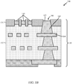
- Fig. 1B depicts a cross section view of the exemplary embodiment shown in Fig. 1A along the indicated cut line.
- semiconductor package 100 may include a substrate 130 having a first dielectric layer 131, a second dielectric layer 132, a padless skip via 160 and a plurality of traces 140 embedded in the first dielectric layer 131. While the embodiment shown includes multiple vias and second dielectric layer regions, this is optional.
- the first dielectric layer 131 may be a photoactive material that may be applied as a liquid or a dry film.
- the second dielectric layer 132 may be a different composition from layer 131 such as a silica based epoxy material.
- the padless skip via 160 may include a body 161, a bottom portion, a top portion 162, and a cover pad 164. The bottom portion may be formed without a landing or capture pad. The top portion may be formed with a cover pad 164.
- the embedded traces 140 may be formed of a conductive material such as copper to facilitate signal routing.
- the traces may be formed with very fine patterning in the dielectric layer 131.
- the very fine patterning may allow low line and space tracing dimensions less than 5 ⁇ m /5 ⁇ m such as 2 ⁇ m /2 ⁇ m.
- the dielectric layer 131 may be a smaller dimension than the dielectric layer 132.
- dielectric layer 131 may be approximately 5-10 ⁇ m thick while the dielectric layer 132 may be approximately 15 ⁇ m thick.
- the padless skip via 160 may have a top portion 162 smaller than a bottom portion. For example, 35 ⁇ m diameter for top portion 162 and 40 ⁇ m diameter for bottom portion.
- the lack of a capture or landing pad for via 160 may allow for higher routing density dielectric layer 131 for additional routing or traces.
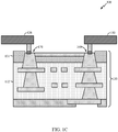
- Fig. 1C depicts a cross section view of the exemplary embodiment shown in Fig. 1A along the indicated cut line.
- semiconductor package 100 may include a first die 110; a second die 120; substrate 130 having a first dielectric layer 131 and a second dielectric layer 132; padless skip vias 160 and 170; and a via trace 150.
- Via trace or routing 150 may connect vias 160 and 170, which in turn may provide a connection between die 110 and 120.
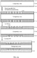
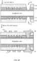
- Fig. 2A depicts an exemplary embodiment of a method for formation of a coreless substrate.
- a temporary core 200 may have a first copper layer 202 and a second copper layer 204. While two copper layers are shown, it should be understood that core 200 may include just one layer and that the layers may be composed of other materials such as conductive metals.
- first dielectric layer 210 is applied to first copper layer 202 and a second dielectric layer 212 is applied to second copper layer 204.
- the first and second dielectric layers 210 and 212 may be a photoactive liquid or dry photoimageable film.
- the first and second dielectric layers 210 and 212 may be layered or cured to a thickness of approximately 5-10 ⁇ m and may include trace patterns 214. While two layers 210 and 212 are shown, it should be understood that only one layer may be used.
- the trace patterns 214 may be very fine and have line space dimensions of less than 5/5 ⁇ m such as 2/2 ⁇ m.
- the layers 210 and 212 may be exposed to light such as UV light and developed to remove the portions in the trace patterns 214.
- the core 200 may be subject to a copper plating process that plates copper in the trace pattern 214 voids.
- the plating process may plate copper in only a portion of the trace pattern 214 voids. This may allow the resulting copper traces 216 to have smaller dimensions that the thickness of the photoactive layer.
- the plating material can be other than copper.
- the photoactive layers 210 and 212 remain after the plating process and are not stripped from the core 200. By avoiding a stripping process, the copper traces conform more readily to the pattern trace since no additional compensation for the trace dimension (trace width) should be done to account for copper seed layer etching or copper roughening steps. This reduces the concern of trace lifting during stripping and etching processes.
- a third dielectric layer 220 is applied to the first dielectric layer 210 and a fourth dielectric layer 222 is applied to second dielectric layer 212.
- the third and fourth dielectric layers 220 and 222 may be a different composition than first and second dielectric layers 210 and 212.
- the composition of layers 220 and 222 may be a non-photoactive material such as a silica based epoxy material.
- the third and fourth layers 220 and 222 may be layered or built up to a thickness greater than that of the first and second layers 210 and 212.
- first and second layers 210 and 212 may be approximately 5-10 ⁇ m and the third and fourth layers 220 and 222 may be approximately 15 ⁇ m.
- Fig. 2B depicts an exemplary embodiment of a method for formation of a coreless substrate.
- a first via 230 and a second via 232 may be formed.
- the first and second vias 230 and 232 may be formed by a chemical or mechanical process such as laser drilling or ablation.
- the first and second vias 230 and 232 may be extended through both dielectric layers 210 and 220 and dielectric layers 212 and 222 respectively.
- the first and second vias may be extended from an outer edge or side of the third and fourth layers 220 and 222 to first and second copper layers 202 and 204.
- SAP semi-additive process
- a semi-additive process including a copper plating process is applied to form a first padless skip via 240 with a cover pad 241 and a second padless via 242 with a cover pad 243 as well as bottom traces 244.
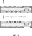
- Figures 3A and 3B depict an exemplary embodiment of a method for formation of a coreless substrate.
- the process illustrated in Fig. 2B is continued.
- additional vias may be formed by adding additional dielectric layers on top of the third and fourth dielectric layers 220 and 222. These additional dielectric layers may then go through the processes depicted in Fig. 2B to form additional vias and via traces.
- the additional vias may be formed by a chemical or mechanical process that extends the via from an outer surface of the added dielectric layer to the cover pad of the previously formed vias. As depicted in Fig.
- the structure may be subject to a SR process that laminates, exposes and develops SR layers 245 and 246 covering bottom traces 244 and portions of cover pads 241 and 243.
- a SR process that laminates, exposes and develops SR layers 245 and 246 covering bottom traces 244 and portions of cover pads 241 and 243.
- the temporary core 200 and copper layers 202 and 204 are removed.
- the core 200 may be separate by a mechanical process and the copper layers 202 and 204 may be etched away after separation.
- the semiconductor structure may include a coreless substrate having a permanent photoactive dielectric layer and an insulating dielectric layer, a plurality of traces embedded in the permanent photoactive dielectric layer, and means for conducting extending through the insulating dielectric layer and the permanent photoimageable dielectric layer.
- the means for conducting provides a path or way to conduct electrical signals (provide an electrical connection) between layers in the semiconductor structure that goes through the plane of one or more adjacent layers.
- the means for conducting may be a via (vertical interconnect access) that provides an opening in one layer for conducting electrical signals between layers.
- the means for conducting may consist of two pads in corresponding positions on different layers of the semiconductor structure that are electrically connected by a hole through the structure.
- the hole may be made conductive by electroplating, lining the hole with conductive material, filling the hole with conductive material, or with a tube or a rivet.
- the means for conducting may be a skip via, microvia, through hole via, through silicon via, blind via, or buried via.
- the means for conducting may include a barrel or conductive tube filling the hole, an antipad or clearance hole between the barrel and a no-connect metal layer, and may optionally include a pad that connects each end of the barrel to a component, plane or trace.
- substitute materials can be used in place of copper.
- the substitute materials can include a mechanical structure that resists etching or a structure that can be coated to resist etching.
- Embodiments of the methods described herein can be used in a number of applications and integrated circuits.
- the described embodiments may be used in a dual die (die partitioning) high density routing between both die to insure proper communication.
- the described embodiments may be used without the use of silicon or organic interposer, which may reduce the cost of fabrication.
- the described embodiments may be used for processors, memory, or power management devices in high density routing application. Further applications should be readily apparent to those of ordinary skill in the art.
- a block or a component of a device should also be understood as a corresponding method step or as a feature of a method step.
- aspects described in connection with or as a method step also constitute a description of a corresponding block or detail or feature of a corresponding device.
- an individual step/action can be subdivided into a plurality of sub-steps or contain a plurality of sub-steps. Such sub-steps can be contained in the disclosure of the individual step and be part of the disclosure of the individual step.
- an embodiment of the disclosure can include a computer readable media embodying a method for location estimation. Accordingly, the disclosure is not limited to illustrated examples and any means for performing the functionality described herein are included in embodiments of the disclosure.
Landscapes
- Engineering & Computer Science (AREA)
- Physics & Mathematics (AREA)
- Condensed Matter Physics & Semiconductors (AREA)
- General Physics & Mathematics (AREA)
- Computer Hardware Design (AREA)
- Microelectronics & Electronic Packaging (AREA)
- Power Engineering (AREA)
- Manufacturing & Machinery (AREA)
- Ceramic Engineering (AREA)
- Internal Circuitry In Semiconductor Integrated Circuit Devices (AREA)
- Production Of Multi-Layered Print Wiring Board (AREA)
- Structure Of Printed Boards (AREA)
Applications Claiming Priority (2)
| Application Number | Priority Date | Filing Date | Title |
|---|---|---|---|
| US14/276,763 US9679841B2 (en) | 2014-05-13 | 2014-05-13 | Substrate and method of forming the same |
| PCT/US2015/027806 WO2015175197A1 (en) | 2014-05-13 | 2015-04-27 | Substrate and method of forming the same |
Publications (2)
| Publication Number | Publication Date |
|---|---|
| EP3143640A1 EP3143640A1 (en) | 2017-03-22 |
| EP3143640B1 true EP3143640B1 (en) | 2020-01-08 |
Family
ID=53180818
Family Applications (1)
| Application Number | Title | Priority Date | Filing Date |
|---|---|---|---|
| EP15722828.9A Active EP3143640B1 (en) | 2014-05-13 | 2015-04-27 | Substrate and method of forming the same |
Country Status (5)
| Country | Link |
|---|---|
| US (1) | US9679841B2 (zh) |
| EP (1) | EP3143640B1 (zh) |
| JP (1) | JP6306743B2 (zh) |
| CN (1) | CN106463447B (zh) |
| WO (1) | WO2015175197A1 (zh) |
Families Citing this family (14)
| Publication number | Priority date | Publication date | Assignee | Title |
|---|---|---|---|---|
| CN107680942B (zh) * | 2016-08-01 | 2019-10-11 | 欣兴电子股份有限公司 | 线路载板及其制作方法 |
| US10340251B2 (en) | 2017-04-26 | 2019-07-02 | Nxp Usa, Inc. | Method for making an electronic component package |
| US10157833B1 (en) * | 2017-05-23 | 2018-12-18 | Globalfoundries Inc. | Via and skip via structures |
| US20180350630A1 (en) * | 2017-06-01 | 2018-12-06 | Qualcomm Incorporated | Symmetric embedded trace substrate |
| US10325842B2 (en) * | 2017-09-08 | 2019-06-18 | Advanced Semiconductor Engineering, Inc. | Substrate for packaging a semiconductor device package and a method of manufacturing the same |
| WO2019066813A1 (en) * | 2017-09-27 | 2019-04-04 | Intel Corporation | METHOD, DEVICE AND SYSTEM FOR PROVIDING GRAZED METALLIZATION STRUCTURES |
| US11387187B2 (en) * | 2018-06-28 | 2022-07-12 | Intel Corporation | Embedded very high density (VHD) layer |
| US10517167B1 (en) * | 2018-10-19 | 2019-12-24 | Eagle Technology, Llc | Systems and methods for providing a high speed interconnect system with reduced crosstalk |
| US10615027B1 (en) | 2018-10-25 | 2020-04-07 | International Business Machines Corporation | Stack viabar structures |
| EP3723459A1 (en) | 2019-04-10 | 2020-10-14 | AT & S Austria Technologie & Systemtechnik Aktiengesellschaft | Component carrier with high passive intermodulation (pim) performance |
| US11056850B2 (en) | 2019-07-26 | 2021-07-06 | Eagle Technology, Llc | Systems and methods for providing a soldered interface on a printed circuit board having a blind feature |
| US11602800B2 (en) | 2019-10-10 | 2023-03-14 | Eagle Technology, Llc | Systems and methods for providing an interface on a printed circuit board using pin solder enhancement |
| US11283204B1 (en) | 2020-11-19 | 2022-03-22 | Eagle Technology, Llc | Systems and methods for providing a composite connector for high speed interconnect systems |
| US20230254980A1 (en) * | 2022-02-07 | 2023-08-10 | Eagle Technology, Llc | Electronic device with multi-diameter female contacts and related methods |
Family Cites Families (19)
| Publication number | Priority date | Publication date | Assignee | Title |
|---|---|---|---|---|
| JP3949849B2 (ja) * | 1999-07-19 | 2007-07-25 | 日東電工株式会社 | チップサイズパッケージ用インターポーザーの製造方法およびチップサイズパッケージ用インターポーザー |
| JP4701506B2 (ja) * | 2000-09-14 | 2011-06-15 | ソニー株式会社 | 回路ブロック体の製造方法、配線回路装置の製造方法並びに半導体装置の製造方法 |
| JP3861669B2 (ja) | 2001-11-22 | 2006-12-20 | ソニー株式会社 | マルチチップ回路モジュールの製造方法 |
| JP2004039867A (ja) * | 2002-07-03 | 2004-02-05 | Sony Corp | 多層配線回路モジュール及びその製造方法 |
| TW561803B (en) | 2002-10-24 | 2003-11-11 | Advanced Semiconductor Eng | Circuit substrate and manufacturing method thereof |
| TWI295550B (en) * | 2005-12-20 | 2008-04-01 | Phoenix Prec Technology Corp | Structure of circuit board and method for fabricating the same |
| US20080169124A1 (en) | 2007-01-12 | 2008-07-17 | Tonglong Zhang | Padless via and method for making same |
| KR20100065691A (ko) | 2008-12-08 | 2010-06-17 | 삼성전기주식회사 | 금속범프를 갖는 인쇄회로기판 및 그 제조방법 |
| US8187920B2 (en) | 2009-02-20 | 2012-05-29 | Texas Instruments Incorporated | Integrated circuit micro-module |
| US7843056B2 (en) * | 2009-02-20 | 2010-11-30 | National Semiconductor Corporation | Integrated circuit micro-module |
| CN102405524A (zh) * | 2009-02-20 | 2012-04-04 | 国家半导体公司 | 集成电路微模块 |
| JP5603600B2 (ja) * | 2010-01-13 | 2014-10-08 | 新光電気工業株式会社 | 配線基板及びその製造方法、並びに半導体パッケージ |
| JP5570855B2 (ja) * | 2010-03-18 | 2014-08-13 | 新光電気工業株式会社 | 配線基板及びその製造方法並びに半導体装置及びその製造方法 |
| US20110272780A1 (en) | 2010-05-05 | 2011-11-10 | Peter Smeys | Method and structure for improving the qualilty factor of rf inductors |
| JP5711472B2 (ja) * | 2010-06-09 | 2015-04-30 | 新光電気工業株式会社 | 配線基板及びその製造方法並びに半導体装置 |
| US8648277B2 (en) | 2011-03-31 | 2014-02-11 | Electro Scientific Industries, Inc. | Laser direct ablation with picosecond laser pulses at high pulse repetition frequencies |
| JP5851211B2 (ja) * | 2011-11-11 | 2016-02-03 | 新光電気工業株式会社 | 半導体パッケージ、半導体パッケージの製造方法及び半導体装置 |
| JP5931547B2 (ja) * | 2012-03-30 | 2016-06-08 | イビデン株式会社 | 配線板及びその製造方法 |
| JP6082233B2 (ja) * | 2012-10-31 | 2017-02-15 | イビデン株式会社 | 配線板及びその製造方法 |
-
2014
- 2014-05-13 US US14/276,763 patent/US9679841B2/en active Active
-
2015
- 2015-04-27 JP JP2016567193A patent/JP6306743B2/ja not_active Expired - Fee Related
- 2015-04-27 CN CN201580024484.6A patent/CN106463447B/zh not_active Expired - Fee Related
- 2015-04-27 WO PCT/US2015/027806 patent/WO2015175197A1/en active Application Filing
- 2015-04-27 EP EP15722828.9A patent/EP3143640B1/en active Active
Non-Patent Citations (1)
| Title |
|---|
| None * |
Also Published As
| Publication number | Publication date |
|---|---|
| EP3143640A1 (en) | 2017-03-22 |
| WO2015175197A1 (en) | 2015-11-19 |
| JP2017516308A (ja) | 2017-06-15 |
| US20150333004A1 (en) | 2015-11-19 |
| JP6306743B2 (ja) | 2018-04-04 |
| CN106463447B (zh) | 2018-06-29 |
| CN106463447A (zh) | 2017-02-22 |
| US9679841B2 (en) | 2017-06-13 |
Similar Documents
| Publication | Publication Date | Title |
|---|---|---|
| EP3143640B1 (en) | Substrate and method of forming the same | |
| US9420693B2 (en) | Integration of embedded thin film capacitors in package substrates | |
| KR101015704B1 (ko) | 칩 내장 인쇄회로기판 및 그 제조방법 | |
| JP4703680B2 (ja) | 埋込型印刷回路基板の製造方法 | |
| US11862552B2 (en) | Methods of embedding magnetic structures in substrates | |
| US20070069360A1 (en) | Semiconductor package substrate having different thicknesses between wire bonding pad and ball pad and method for fabricating the same | |
| KR101067199B1 (ko) | 인쇄회로기판 및 그 제조방법 | |
| KR20110095146A (ko) | 다층 배선기판 및 그 제조방법 | |
| JP2009283739A (ja) | 配線基板および配線基板の製造方法 | |
| EP3557957A1 (en) | Wiring substrate, multilayer wiring substrate, and method for manufacturing wiring substrate | |
| US10483194B2 (en) | Interposer substrate and method of fabricating the same | |
| WO2015112695A1 (en) | Substrate and method of forming the same | |
| CN105830213A (zh) | 包括凸块区域中的改善型通孔焊盘放置的基板 | |
| KR100972431B1 (ko) | 임베디드 인쇄회로기판 및 그 제조방법 | |
| US20080123309A1 (en) | Slim design main board | |
| KR100704911B1 (ko) | 전자소자 내장형 인쇄회로기판 및 그 제조방법 | |
| KR100689018B1 (ko) | 동축 선로가 내장된 인쇄 회로 기판 및 제조 방법 | |
| US10026691B2 (en) | Package substrate having noncircular interconnects | |
| US20130153275A1 (en) | Printed circuit board and method for manufacturing the same | |
| CN107507819B (zh) | 一种基于电容芯板的无源器件集成方法 | |
| US20240164013A1 (en) | Printed circuit board and manufacturing method for the same | |
| KR100443736B1 (ko) | 범프를 이용한 고집적 인쇄회로기판의 제조 방법 | |
| JP2008124260A (ja) | 多層配線基板及びその製造方法 | |
| KR20170087765A (ko) | 인쇄회로기판 | |
| US20130146337A1 (en) | Multi-layered printed circuit board and manufacturing method thereof |
Legal Events
| Date | Code | Title | Description |
|---|---|---|---|
| STAA | Information on the status of an ep patent application or granted ep patent |
Free format text: STATUS: THE INTERNATIONAL PUBLICATION HAS BEEN MADE |
|
| PUAI | Public reference made under article 153(3) epc to a published international application that has entered the european phase |
Free format text: ORIGINAL CODE: 0009012 |
|
| STAA | Information on the status of an ep patent application or granted ep patent |
Free format text: STATUS: REQUEST FOR EXAMINATION WAS MADE |
|
| 17P | Request for examination filed |
Effective date: 20161122 |
|
| AK | Designated contracting states |
Kind code of ref document: A1 Designated state(s): AL AT BE BG CH CY CZ DE DK EE ES FI FR GB GR HR HU IE IS IT LI LT LU LV MC MK MT NL NO PL PT RO RS SE SI SK SM TR |
|
| AX | Request for extension of the european patent |
Extension state: BA ME |
|
| DAV | Request for validation of the european patent (deleted) | ||
| DAX | Request for extension of the european patent (deleted) | ||
| STAA | Information on the status of an ep patent application or granted ep patent |
Free format text: STATUS: EXAMINATION IS IN PROGRESS |
|
| 17Q | First examination report despatched |
Effective date: 20180716 |
|
| GRAP | Despatch of communication of intention to grant a patent |
Free format text: ORIGINAL CODE: EPIDOSNIGR1 |
|
| STAA | Information on the status of an ep patent application or granted ep patent |
Free format text: STATUS: GRANT OF PATENT IS INTENDED |
|
| RIC1 | Information provided on ipc code assigned before grant |
Ipc: H01L 21/48 20060101AFI20181128BHEP Ipc: H01L 23/538 20060101ALI20181128BHEP |
|
| INTG | Intention to grant announced |
Effective date: 20181217 |
|
| GRAS | Grant fee paid |
Free format text: ORIGINAL CODE: EPIDOSNIGR3 |
|
| GRAJ | Information related to disapproval of communication of intention to grant by the applicant or resumption of examination proceedings by the epo deleted |
Free format text: ORIGINAL CODE: EPIDOSDIGR1 |
|
| GRAL | Information related to payment of fee for publishing/printing deleted |
Free format text: ORIGINAL CODE: EPIDOSDIGR3 |
|
| STAA | Information on the status of an ep patent application or granted ep patent |
Free format text: STATUS: EXAMINATION IS IN PROGRESS |
|
| INTC | Intention to grant announced (deleted) | ||
| GRAP | Despatch of communication of intention to grant a patent |
Free format text: ORIGINAL CODE: EPIDOSNIGR1 |
|
| STAA | Information on the status of an ep patent application or granted ep patent |
Free format text: STATUS: GRANT OF PATENT IS INTENDED |
|
| INTG | Intention to grant announced |
Effective date: 20190731 |
|
| GRAA | (expected) grant |
Free format text: ORIGINAL CODE: 0009210 |
|
| STAA | Information on the status of an ep patent application or granted ep patent |
Free format text: STATUS: THE PATENT HAS BEEN GRANTED |
|
| AK | Designated contracting states |
Kind code of ref document: B1 Designated state(s): AL AT BE BG CH CY CZ DE DK EE ES FI FR GB GR HR HU IE IS IT LI LT LU LV MC MK MT NL NO PL PT RO RS SE SI SK SM TR |
|
| REG | Reference to a national code |
Ref country code: GB Ref legal event code: FG4D |
|
| REG | Reference to a national code |
Ref country code: CH Ref legal event code: EP |
|
| REG | Reference to a national code |
Ref country code: DE Ref legal event code: R096 Ref document number: 602015045116 Country of ref document: DE |
|
| REG | Reference to a national code |
Ref country code: IE Ref legal event code: FG4D |
|
| REG | Reference to a national code |
Ref country code: AT Ref legal event code: REF Ref document number: 1223731 Country of ref document: AT Kind code of ref document: T Effective date: 20200215 |
|
| REG | Reference to a national code |
Ref country code: NL Ref legal event code: MP Effective date: 20200108 |
|
| REG | Reference to a national code |
Ref country code: LT Ref legal event code: MG4D |
|
| PG25 | Lapsed in a contracting state [announced via postgrant information from national office to epo] |
Ref country code: LT Free format text: LAPSE BECAUSE OF FAILURE TO SUBMIT A TRANSLATION OF THE DESCRIPTION OR TO PAY THE FEE WITHIN THE PRESCRIBED TIME-LIMIT Effective date: 20200108 Ref country code: NL Free format text: LAPSE BECAUSE OF FAILURE TO SUBMIT A TRANSLATION OF THE DESCRIPTION OR TO PAY THE FEE WITHIN THE PRESCRIBED TIME-LIMIT Effective date: 20200108 Ref country code: NO Free format text: LAPSE BECAUSE OF FAILURE TO SUBMIT A TRANSLATION OF THE DESCRIPTION OR TO PAY THE FEE WITHIN THE PRESCRIBED TIME-LIMIT Effective date: 20200408 Ref country code: PT Free format text: LAPSE BECAUSE OF FAILURE TO SUBMIT A TRANSLATION OF THE DESCRIPTION OR TO PAY THE FEE WITHIN THE PRESCRIBED TIME-LIMIT Effective date: 20200531 Ref country code: RS Free format text: LAPSE BECAUSE OF FAILURE TO SUBMIT A TRANSLATION OF THE DESCRIPTION OR TO PAY THE FEE WITHIN THE PRESCRIBED TIME-LIMIT Effective date: 20200108 Ref country code: FI Free format text: LAPSE BECAUSE OF FAILURE TO SUBMIT A TRANSLATION OF THE DESCRIPTION OR TO PAY THE FEE WITHIN THE PRESCRIBED TIME-LIMIT Effective date: 20200108 |
|
| PG25 | Lapsed in a contracting state [announced via postgrant information from national office to epo] |
Ref country code: BG Free format text: LAPSE BECAUSE OF FAILURE TO SUBMIT A TRANSLATION OF THE DESCRIPTION OR TO PAY THE FEE WITHIN THE PRESCRIBED TIME-LIMIT Effective date: 20200408 Ref country code: IS Free format text: LAPSE BECAUSE OF FAILURE TO SUBMIT A TRANSLATION OF THE DESCRIPTION OR TO PAY THE FEE WITHIN THE PRESCRIBED TIME-LIMIT Effective date: 20200508 Ref country code: GR Free format text: LAPSE BECAUSE OF FAILURE TO SUBMIT A TRANSLATION OF THE DESCRIPTION OR TO PAY THE FEE WITHIN THE PRESCRIBED TIME-LIMIT Effective date: 20200409 Ref country code: LV Free format text: LAPSE BECAUSE OF FAILURE TO SUBMIT A TRANSLATION OF THE DESCRIPTION OR TO PAY THE FEE WITHIN THE PRESCRIBED TIME-LIMIT Effective date: 20200108 Ref country code: SE Free format text: LAPSE BECAUSE OF FAILURE TO SUBMIT A TRANSLATION OF THE DESCRIPTION OR TO PAY THE FEE WITHIN THE PRESCRIBED TIME-LIMIT Effective date: 20200108 Ref country code: HR Free format text: LAPSE BECAUSE OF FAILURE TO SUBMIT A TRANSLATION OF THE DESCRIPTION OR TO PAY THE FEE WITHIN THE PRESCRIBED TIME-LIMIT Effective date: 20200108 |
|
| REG | Reference to a national code |
Ref country code: DE Ref legal event code: R097 Ref document number: 602015045116 Country of ref document: DE |
|
| PG25 | Lapsed in a contracting state [announced via postgrant information from national office to epo] |
Ref country code: ES Free format text: LAPSE BECAUSE OF FAILURE TO SUBMIT A TRANSLATION OF THE DESCRIPTION OR TO PAY THE FEE WITHIN THE PRESCRIBED TIME-LIMIT Effective date: 20200108 Ref country code: DK Free format text: LAPSE BECAUSE OF FAILURE TO SUBMIT A TRANSLATION OF THE DESCRIPTION OR TO PAY THE FEE WITHIN THE PRESCRIBED TIME-LIMIT Effective date: 20200108 Ref country code: CZ Free format text: LAPSE BECAUSE OF FAILURE TO SUBMIT A TRANSLATION OF THE DESCRIPTION OR TO PAY THE FEE WITHIN THE PRESCRIBED TIME-LIMIT Effective date: 20200108 Ref country code: SM Free format text: LAPSE BECAUSE OF FAILURE TO SUBMIT A TRANSLATION OF THE DESCRIPTION OR TO PAY THE FEE WITHIN THE PRESCRIBED TIME-LIMIT Effective date: 20200108 Ref country code: RO Free format text: LAPSE BECAUSE OF FAILURE TO SUBMIT A TRANSLATION OF THE DESCRIPTION OR TO PAY THE FEE WITHIN THE PRESCRIBED TIME-LIMIT Effective date: 20200108 Ref country code: EE Free format text: LAPSE BECAUSE OF FAILURE TO SUBMIT A TRANSLATION OF THE DESCRIPTION OR TO PAY THE FEE WITHIN THE PRESCRIBED TIME-LIMIT Effective date: 20200108 Ref country code: SK Free format text: LAPSE BECAUSE OF FAILURE TO SUBMIT A TRANSLATION OF THE DESCRIPTION OR TO PAY THE FEE WITHIN THE PRESCRIBED TIME-LIMIT Effective date: 20200108 |
|
| PLBE | No opposition filed within time limit |
Free format text: ORIGINAL CODE: 0009261 |
|
| STAA | Information on the status of an ep patent application or granted ep patent |
Free format text: STATUS: NO OPPOSITION FILED WITHIN TIME LIMIT |
|
| REG | Reference to a national code |
Ref country code: AT Ref legal event code: MK05 Ref document number: 1223731 Country of ref document: AT Kind code of ref document: T Effective date: 20200108 |
|
| PG25 | Lapsed in a contracting state [announced via postgrant information from national office to epo] |
Ref country code: MC Free format text: LAPSE BECAUSE OF FAILURE TO SUBMIT A TRANSLATION OF THE DESCRIPTION OR TO PAY THE FEE WITHIN THE PRESCRIBED TIME-LIMIT Effective date: 20200108 |
|
| REG | Reference to a national code |
Ref country code: CH Ref legal event code: PL |
|
| 26N | No opposition filed |
Effective date: 20201009 |
|
| PG25 | Lapsed in a contracting state [announced via postgrant information from national office to epo] |
Ref country code: IT Free format text: LAPSE BECAUSE OF FAILURE TO SUBMIT A TRANSLATION OF THE DESCRIPTION OR TO PAY THE FEE WITHIN THE PRESCRIBED TIME-LIMIT Effective date: 20200108 Ref country code: AT Free format text: LAPSE BECAUSE OF FAILURE TO SUBMIT A TRANSLATION OF THE DESCRIPTION OR TO PAY THE FEE WITHIN THE PRESCRIBED TIME-LIMIT Effective date: 20200108 Ref country code: LU Free format text: LAPSE BECAUSE OF NON-PAYMENT OF DUE FEES Effective date: 20200427 Ref country code: CH Free format text: LAPSE BECAUSE OF NON-PAYMENT OF DUE FEES Effective date: 20200430 Ref country code: LI Free format text: LAPSE BECAUSE OF NON-PAYMENT OF DUE FEES Effective date: 20200430 |
|
| REG | Reference to a national code |
Ref country code: BE Ref legal event code: MM Effective date: 20200430 |
|
| PG25 | Lapsed in a contracting state [announced via postgrant information from national office to epo] |
Ref country code: PL Free format text: LAPSE BECAUSE OF FAILURE TO SUBMIT A TRANSLATION OF THE DESCRIPTION OR TO PAY THE FEE WITHIN THE PRESCRIBED TIME-LIMIT Effective date: 20200108 Ref country code: BE Free format text: LAPSE BECAUSE OF NON-PAYMENT OF DUE FEES Effective date: 20200430 Ref country code: SI Free format text: LAPSE BECAUSE OF FAILURE TO SUBMIT A TRANSLATION OF THE DESCRIPTION OR TO PAY THE FEE WITHIN THE PRESCRIBED TIME-LIMIT Effective date: 20200108 |
|
| PG25 | Lapsed in a contracting state [announced via postgrant information from national office to epo] |
Ref country code: IE Free format text: LAPSE BECAUSE OF NON-PAYMENT OF DUE FEES Effective date: 20200427 |
|
| PG25 | Lapsed in a contracting state [announced via postgrant information from national office to epo] |
Ref country code: TR Free format text: LAPSE BECAUSE OF FAILURE TO SUBMIT A TRANSLATION OF THE DESCRIPTION OR TO PAY THE FEE WITHIN THE PRESCRIBED TIME-LIMIT Effective date: 20200108 Ref country code: MT Free format text: LAPSE BECAUSE OF FAILURE TO SUBMIT A TRANSLATION OF THE DESCRIPTION OR TO PAY THE FEE WITHIN THE PRESCRIBED TIME-LIMIT Effective date: 20200108 Ref country code: CY Free format text: LAPSE BECAUSE OF FAILURE TO SUBMIT A TRANSLATION OF THE DESCRIPTION OR TO PAY THE FEE WITHIN THE PRESCRIBED TIME-LIMIT Effective date: 20200108 |
|
| PG25 | Lapsed in a contracting state [announced via postgrant information from national office to epo] |
Ref country code: MK Free format text: LAPSE BECAUSE OF FAILURE TO SUBMIT A TRANSLATION OF THE DESCRIPTION OR TO PAY THE FEE WITHIN THE PRESCRIBED TIME-LIMIT Effective date: 20200108 Ref country code: AL Free format text: LAPSE BECAUSE OF FAILURE TO SUBMIT A TRANSLATION OF THE DESCRIPTION OR TO PAY THE FEE WITHIN THE PRESCRIBED TIME-LIMIT Effective date: 20200108 |
|
| PGFP | Annual fee paid to national office [announced via postgrant information from national office to epo] |
Ref country code: FR Payment date: 20230320 Year of fee payment: 9 |
|
| PGFP | Annual fee paid to national office [announced via postgrant information from national office to epo] |
Ref country code: DE Payment date: 20230320 Year of fee payment: 9 |
|
| PGFP | Annual fee paid to national office [announced via postgrant information from national office to epo] |
Ref country code: GB Payment date: 20240314 Year of fee payment: 10 |