EP3126852B1 - Système de mise en contact, en particulier pointe de mesure hf - Google Patents
Système de mise en contact, en particulier pointe de mesure hf Download PDFInfo
- Publication number
- EP3126852B1 EP3126852B1 EP15700416.9A EP15700416A EP3126852B1 EP 3126852 B1 EP3126852 B1 EP 3126852B1 EP 15700416 A EP15700416 A EP 15700416A EP 3126852 B1 EP3126852 B1 EP 3126852B1
- Authority
- EP
- European Patent Office
- Prior art keywords
- conductor
- contact
- impedance
- contacting assembly
- carrier
- Prior art date
- Legal status (The legal status is an assumption and is not a legal conclusion. Google has not performed a legal analysis and makes no representation as to the accuracy of the status listed.)
- Active
Links
- 239000004020 conductor Substances 0.000 claims description 155
- 238000012360 testing method Methods 0.000 claims description 16
- 230000009466 transformation Effects 0.000 claims description 15
- 239000000523 sample Substances 0.000 description 8
- 230000008859 change Effects 0.000 description 6
- 239000004575 stone Substances 0.000 description 6
- WYTGDNHDOZPMIW-RCBQFDQVSA-N alstonine Natural products C1=CC2=C3C=CC=CC3=NC2=C2N1C[C@H]1[C@H](C)OC=C(C(=O)OC)[C@H]1C2 WYTGDNHDOZPMIW-RCBQFDQVSA-N 0.000 description 4
- 238000005259 measurement Methods 0.000 description 4
- 238000010079 rubber tapping Methods 0.000 description 4
- 239000002184 metal Substances 0.000 description 3
- 235000012431 wafers Nutrition 0.000 description 3
- 238000000034 method Methods 0.000 description 2
- 230000008569 process Effects 0.000 description 2
- 238000006243 chemical reaction Methods 0.000 description 1
- 230000008878 coupling Effects 0.000 description 1
- 238000010168 coupling process Methods 0.000 description 1
- 238000005859 coupling reaction Methods 0.000 description 1
- 230000003247 decreasing effect Effects 0.000 description 1
- 230000001419 dependent effect Effects 0.000 description 1
- 238000013461 design Methods 0.000 description 1
- 238000011161 development Methods 0.000 description 1
- 230000018109 developmental process Effects 0.000 description 1
- 230000013011 mating Effects 0.000 description 1
- 239000004065 semiconductor Substances 0.000 description 1
- 238000000742 single-metal deposition Methods 0.000 description 1
- 230000007704 transition Effects 0.000 description 1
Images

Classifications
-
- G—PHYSICS
- G01—MEASURING; TESTING
- G01R—MEASURING ELECTRIC VARIABLES; MEASURING MAGNETIC VARIABLES
- G01R1/00—Details of instruments or arrangements of the types included in groups G01R5/00 - G01R13/00 and G01R31/00
- G01R1/02—General constructional details
- G01R1/06—Measuring leads; Measuring probes
- G01R1/067—Measuring probes
- G01R1/06772—High frequency probes
-
- G—PHYSICS
- G01—MEASURING; TESTING
- G01R—MEASURING ELECTRIC VARIABLES; MEASURING MAGNETIC VARIABLES
- G01R15/00—Details of measuring arrangements of the types provided for in groups G01R17/00 - G01R29/00, G01R33/00 - G01R33/26 or G01R35/00
- G01R15/14—Adaptations providing voltage or current isolation, e.g. for high-voltage or high-current networks
-
- G—PHYSICS
- G01—MEASURING; TESTING
- G01R—MEASURING ELECTRIC VARIABLES; MEASURING MAGNETIC VARIABLES
- G01R31/00—Arrangements for testing electric properties; Arrangements for locating electric faults; Arrangements for electrical testing characterised by what is being tested not provided for elsewhere
- G01R31/28—Testing of electronic circuits, e.g. by signal tracer
-
- G—PHYSICS
- G01—MEASURING; TESTING
- G01R—MEASURING ELECTRIC VARIABLES; MEASURING MAGNETIC VARIABLES
- G01R1/00—Details of instruments or arrangements of the types included in groups G01R5/00 - G01R13/00 and G01R31/00
- G01R1/02—General constructional details
- G01R1/06—Measuring leads; Measuring probes
- G01R1/067—Measuring probes
- G01R1/06766—Input circuits therefor
Definitions
- the invention relates to a Kunststoffieran Aunt for tapping and forwarding a voltage, in particular a radio frequency (RF) probe or RF probe, with a carrier on which a conductor pattern is arranged, wherein the conductor structure at a contact-side end at least one over an edge of the carrier projecting contact element for electrically contacting at least one contact point of a device under test, and wherein the line structure has at least one impedance transformer or impedance transformer.
- RF radio frequency
- the measuring tip must have an impedance adapted to the electronic circuit to be tested of the test object at its contact-side end, since otherwise, in the case of mismatches, as is generally known, reflections can arise which can undesirably influence a measurement result or make a measurement impossible ,
- a coaxial cable or a circuit having a predetermined impedance of, for example, 50 ⁇ or another connection element with a predetermined impedance is connected to a connection-side end of the conductor structure remote from the contact-side end of the conductor structure for forwarding the signals or voltages picked up by the test object, it can be necessary to incorporate an impedance converter in the conductor structure on the support, so that the measuring tip can be used without unwanted reflections for measuring a test specimen with deviating impedance.
- an impedance converter As such an impedance converter, a passive device such as an RF transformer or other surface-mounted device SMD may be considered. However, such an impedance converter is usable only for impedance transformation over a limited frequency range. If the RF signals conducted from the test specimen through the probe tip are outside this frequency band, unwanted reflections are produced by the impedance transducer.
- the WO 03/012461 A1 discloses a measurement arrangement for high frequency measurements with multiple probes for contacting conductor patterns on wafers and the like.
- the probes comprise coplanar and cantilevered contact tips which are fixed by means of at least one support near their contact-side end so that they have a fixed position to each other.
- the measuring arrangement according to the WO 03/012461 A1 also has a conductor section designed as an impedance converter with a tapered or widening cross section.
- a Kunststoffieran Aunt such as an RF probe tip, which for a wide frequency band, the signal to be measured passes without reflection and is particularly flexible.
- the impedance converter of the contacting arrangement according to the invention is characterized in that it has an electrical conductor section with a gradually tapered or widening cross section.
- the invention is based on the recognition that for impedance transformation, not necessarily a complex electronic component such as a Balun o. The like. Is required. Rather, it is sufficient for impedance conversion to use a conductor section with gradually changing conductor cross-section between the contact-side end and the connection-side end of the conductor structure.
- the length and the change in cross section of this conductor section are set up such that the characteristic impedance of the conductor structure changes by a predetermined value. Since a step change in the conductor cross-section regularly leads to reflections, the change in the conductor cross-section is preferably carried out gradually, preferably over a distance of more than 5 cm, more preferably more than 10 cm, in particular 20 cm or more.
- the contacting arrangement has five contact elements projecting from the carrier, of which at least two contact elements are connected to at least one ground conductor arranged on the carrier, which preferably extends from the contact-side end to the connection-side end.
- reflections can be introduced by an abruptly changing conductor cross-section.
- An abrupt change in the cross section or conductor width change at the transition between the conductor track and the narrow contact element at the contact-side end of the conductor structure can be reduced by electrically connecting five spaced-apart contact elements to the conductor track.
- the conductor track is fanned out by being connected to more than one contact element projecting from the carrier, wherein in each case one ground contact element connected to the ground conductor can be arranged between the individual signal-carrying contact elements. In this way, the width of the track at the contact-side end to the tips of the contact elements can be practically continued.
- An alternating arrangement of ground contact elements and signal-carrying contact elements in this case increases the distance between the individual contact elements while maintaining a low-impedance input impedance. If, for example, only one signal-carrying contact element and one ground contact element are present next to one another, their distance to maintain a low-impedance input impedance may need to be set to less than 1 ⁇ m. Such a small distance between two contact elements is difficult to produce and the corresponding contact elements are prone to damage. On the other hand, if three or more signal-carrying contact elements each protrude between ground contact elements of the carrier, a mutual distance of adjacent contact elements of more than 10 microns may be sufficient.
- the conductor structure has at least one signal conductor or voltage conductor and at least one ground conductor, which each extend from the contact-side end to the connection-side end, wherein a connector for forwarding the tapped signal can be arranged at the connection-side end of the conductor structure.
- the conductor section with a changing cross section is preferably installed in the signal conductor.
- the ground conductor like the signal conductor, may be connected to one or more contact elements projecting from the carrier for electrically contacting at least one contact point of the device under test at the contact-side end.
- the carrier may comprise a dielectric, on which the conductor structure is arranged.
- the carrier is formed in the form of a printed circuit board, on which a part of the conductor structure is applied as a conductor track.
- the conductor section of varying cross section may be formed as a (substantially two-dimensional, thus applied flat) conductor track with decreasing or increasing width.
- the signal conductor is at least partially formed as a conductor, while the ground conductor, for example, can be arranged as a cover layer of a conductive material such as metal on a back side of the circuit board.
- the ratio between the track width at the one end of the track and the track width at the other end of the track is preferably greater than two, more preferably greater than three, in particular four or more. This ratio depends on the impedance transformation to be achieved.
- the impedance converter comprises a knocking stone structure or a "tapping stone taper".
- a tapping stone taper two different predetermined wave resistance levels are interconnected by a tapered cross-section conductor section along a short path while minimizing reflections.
- an impedance transformation over a particularly wide RF frequency band is possible without disturbing reflections.
- a particularly compact and cost-producible contacting arrangement can be provided in that the conductor section extends from the connection-side end in the direction of the contact-side end at least in sections curvy, in particular meandering.
- the tapered conductor section runs serpentine and preferably has several, more preferably more than five, in particular seven or more curved sections, in which the direction of the conductor section is reversed by approximately 180 °.
- a conductor length of, for example, more than 30 cm can be applied to a carrier region having a length of, for example, less than 10 cm.
- the ratio between the length of the conductor portion and the longitudinal dimension of the support portion on which the conductor portion is disposed is three or more.
- the contacting arrangement according to the invention can be produced in a particularly simple manner in that a serpentine conductor section in the form of a conductor track is printed on a printed circuit board or applied in another way.
- the tapered conductor section can also be formed linearly, ie without curves or curves, on the carrier.
- the conductor section preferably in the form of a conductor track over more than 50%, preferably over more than 80%, in particular over the entire dimension of Carrier extends from the contact-side end to the connection-side end.
- This dimension may advantageously be more than 6 cm and less than 20 cm, in particular between 10 and 15 cm.
- an impedance converter having a knockstone taper for impedance transformation over a particularly wide frequency range from about 700 MHz to about 2.7 GHz, preferably from 500 MHz to 3 GHz, particularly preferably from 400 MHz to 10 GHz, In particular, from 300 MHz to 20 GHz can be set up, wherein the reflection factor ⁇ over the entire frequency range is less than 0.2, in particular less than 0.1.
- the output impedance of the conductor pattern is understood to mean the impedance of the conductor pattern at the connection-side end between the signal conductor having the conductor portion and a ground conductor (connection-side impedance).
- the input impedance of the conductor structure is understood to mean the contact-side impedance of the conductor structure between the contact element connected to the conductor section and a contact element connected to the ground conductor, which is adapted to the wave impedance of the test object to be measured.
- the contact-side impedance of the conductor structure is preferably about 10 ⁇ or about 12.5 ⁇ and / or the connection-side impedance of the conductor structure about 50 ⁇ or vice versa.
- a conventional coaxial cable can be connected to the connection-side end of the contacting arrangement.
- the at least one contact element is a preferably resiliently arranged contact fingers.
- all Contact elements including the mass contact connected to the ground contact elements formed as a resilient contact fingers.
- the plurality of contact spring-like protruding over a support edge contact elements may be arranged coplanar, so that they are adapted to contact coplanar contact points of the specimen.
- two outer contact elements are mass elements connected to the ground conductor, while a middle contact element is connected to the signal conductor having the tapered conductor portion.
- the mutual distance and the length of the contact elements are each arranged such that a predetermined wave impedance results at the contact-side end, which is adapted to the wave impedance of the test object.
- the at least one ground conductor can be arranged on that surface of the carrier which is remote from the surface carrying the conductor section. It may be formed as a metal layer or metal ceiling that covers a back of the wearer. Alternatively or additionally, a shielding of the signal conductor of the conductor structure may be provided.
- Such a contact element structure may be referred to as a GSG structure (ground signal ground).
- the two outer contact elements are ground contact elements, of which preferably four or more are present.
- the contact structure preferably has three or more signal-carrying contact elements connected to the conductor track, which project in each case between two ground contact elements.
- the conductor structure can be connected to the contact-side end facing away from the connection-side end having a connection element such as a connector, in particular a coaxial connector, wherein preferably a ground conductor of the contact structure with an outer conductor of the connector and / or the conductor portion of the contact structure is connected to an inner conductor of the connector.
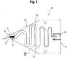
- semiconductor wafers comprises a printed circuit board having a carrier 12, starting from a connection-side end 14 in the direction of a contact end 16 gradually tapered.
- a conductor structure 20 is arranged, which extends from the connection-side end 14 to the contact-side end 16.
- the conductor structure 20 has at least one signal conductor and at least one ground conductor, the ground conductor being arranged on the rear side of the carrier 12, not shown, while the surface of the carrier 12 carrying the signal conductor faces the viewer in the illustrated figure.
- the conductor structure 20 may also have a plurality of signal conductors.
- signal and ground conductors may be disposed on the same surface of the carrier 12.
- the carrier 12 From the contact-side end 16 of the carrier 12, there are a total of three resilient contact elements 22 in the form of contact fingers 23 over a carrier edge, which are provided for contacting appropriately spaced contact points of the test object.
- the middle contact finger 23 with the signal conductor and the outer two contact fingers 23 are connected to the ground conductor.
- the outer contact fingers 23 are thus ground contact elements 21.
- Other arrangements of the contact elements or more than three contact fingers are equally conceivable.
- a connector 40 having an inner conductor and an outer conductor is arranged at the connection-side end 14 of the carrier 14.
- a coaxial cable or a mating connector can be plugged into the connector 40 for forwarding the tapped via the contact elements 22 RF signals.
- the inner conductor of the connector 40 is electrically connected to the signal conductor and thus to the middle contact finger 23, while the outer conductor of the connector 40 is electrically connected to the ground conductor and thus to the two ground contact elements 21.
- the conductor structure 20 has an impedance converter 24, wherein the impedance converter 24 has an electrical conductor section 26 with starting from the connection-side end 14 in the direction of the contact-side end 16 gradually widening cross-section.
- This conductor section 26 is provided in the illustrated exemplary embodiment in the form of an applied on the support 12 conductor 27 with increasing width.
- the conductor 27 is part of the signal conductor which extends between the middle contact finger 23 and the inner conductor of the connector 40.
- the geometric shape and the course of the conductor track 27 are set up in such a way that a knocking stone structure results for the impedance transformation between the connection-side end 14 and the contact-side end 16.
- 23 signals of a test object with a wave impedance of 12.5 ⁇ can be tapped by the contact fingers 23 and forwarded via a be connected to the connector 40 coaxial cable with a wave impedance of 50 ⁇ without reflection.
- the illustrated Kunststoffieran Aunt 10 is an impedance converter in total, in which the impedance transformation takes place by means of a knock stone structure.
- the Kunststoffieran Aunt 10 is adapted for tapping and forwarding of RF signals over a frequency band of about 698 MHz to about 2.7 GHz, without reflections occur, the impedance level of 12.5 ⁇ at the contact-side end 16 of the conductor structure 20 on 50 ⁇ is raised at the connection-side end of the conductor pattern 20. This results in the present example, a transformation ratio of 1: 4. Alternatively, the impedance level may be raised from 10 ⁇ at the contact-side end 16 to 50 ⁇ at the connection-side end, resulting in a transformation ratio of 1: 5.
- a more compact design of the Kunststoffieranssen 10 is possible in that the conductor 27 between the connector 40 and the contact finger 23 is serpentine and has a plurality of curves.
- the width of the conductor 27 on the contact element 22 facing the end of the conductor 27 is about 4 times as large as the width of the connector 40 facing the end.
- the shape, length and course of the track 27 can be adjusted accordingly depending on the impedance transformation to be achieved.
- the distance and the length of the contact elements 22 are arranged such that the contact-side impedance is adapted to the impedance of the component to be measured.
- the impedance transformation is carried out solely by the course of the conductor 27 of the signal conductor, without additional components such as SMDs are required.
- the frequency band can be made broadband and the contacting according to the invention thus be used for testing LTE components.
- the transformation ratio of the impedance converter can be varied individually and can be, for example, 1: 5, 5: 1, 1: 2, 2: 1, 1: 4, 4: 1, etc.
- Fig. 2 shows an exemplary second embodiment of a Maisieran Aunt 10 'according to the invention.
- the conductor section 26 'in the form of a conductor track 27' is not serpentine, but extends linearly from the plug-side end 14 to the contact-side End 16 via the carrier 12.
- the overall dimension of the carrier which corresponds essentially to the length of the tapered in the direction of the connection-side end 14 trace 27 ', is about 12 cm.
- the straight course of the conductor section 26 ' prevents crosstalk between individual conductor loops.
- the conductor structure 20 has a total of seven over an edge of the carrier 12 projecting contact elements 22, of which four ground contact elements 21 are each connected to a (common) ground conductor on the back of the carrier 12 and three signal-carrying contact elements with the conductor track 27 'are connected.
- the ground contact elements 21 and the signal-carrying contact elements change.
- the two outer contact elements 22 are ground contact elements 21.
- more or less than seven contact elements 22 are conceivable.
- the fanning out into a plurality of contact elements connected to the conductor section 26 ' minimizes reflection at the junction between the contact elements 22 and the (broad) end of the conductor section 26'. Furthermore, the distance between the individual contact elements 22 can be set larger in this way while maintaining the desired contact-side impedance. In the present case, the distance between two adjacent contact elements 22 is more than 10 ⁇ m and the contact-side impedance is about 10 ⁇ . The mutual distance and the number of contact elements can be adjusted accordingly depending on the desired impedance transformation.
Landscapes
- Physics & Mathematics (AREA)
- General Physics & Mathematics (AREA)
- Engineering & Computer Science (AREA)
- General Engineering & Computer Science (AREA)
- Measuring Leads Or Probes (AREA)
- Testing Or Measuring Of Semiconductors Or The Like (AREA)
- Tests Of Electronic Circuits (AREA)
Claims (11)
- Ensemble de mise en contact (10 ; 10'), en particulier pointe de mesure HF, comportant un support (12) sur lequel est agencée une structure conductrice (20),
dans lequel
la structure conductrice (20) présente, à une extrémité (16) côté contact, au moins cinq éléments de contact (22) saillant du support et destinés à la mise en contact électrique d'au moins un emplacement de contact d'une éprouvette,
la structure conductrice (20) présente un transformateur d'impédance (24), le transformateur d'impédance (24) présente une portion conductrice (26 ; 26') ayant une section transversale qui se rétrécit ou s'élargit progressivement,
parmi lesdits éléments de contact (22), deux éléments de contact (22) réalisés sous forme d'éléments de contact de masse (21) sont connectés à un conducteur de masse disposé sur le support (12), et les trois éléments de contact restants sont connectés à la portion conductrice (26 ; 26'),
le conducteur de masse s'étend en partant de l'extrémité (16) côté contact jusqu'à une extrémité (14) côté connexion, et
les éléments de contact (22) saillant du support (12) sont connectés électriquement en alternance au conducteur de masse et à la portion conductrice (26 ; 26'). - Ensemble de mise en contact selon la revendication 1,
caractérisé en ce que
la portion conductrice (26 ; 26') est une piste conductrice (27 ; 27') ayant une largeur qui diminue ou augmente progressivement et étant déposée sur un diélectrique, en particulier sur une carte à circuits. - Ensemble de mise en contact selon la revendication 1 ou 2,
caractérisé en ce que
le transformateur d'impédance (24) comprend une structure dite de Klopfenstein. - Ensemble de mise en contact (10) selon l'une au moins des revendications précédentes,
caractérisé en ce que
la portion conductrice (26) s'étend au moins localement sous forme incurvée, en particulier en forme de méandres ou en forme de serpentin. - Ensemble de mise en contact (10') selon l'une au moins des revendications 1 à 3,
caractérisé en ce que
la portion conductrice (26') s'étend au moins sensiblement linéairement et s'étend de préférence sur plus de 50 %, en particulier sur 80 % ou plus de l'extension du support (12). - Ensemble de mise en contact (10) selon l'une au moins des revendications précédentes,
caractérisé en ce que
le transformateur d'impédance (24) est conçu pour une transformation d'impédance sur une bande de fréquence d'environ 700 MHz à environ 2,7 GHz, de préférence de 500 MHz à 3 GHz, de manière particulièrement préférée de 400 MHz à 10 GHz, en particulier de 300 MHz à 20 GHz. - Ensemble de mise en contact (10) selon l'une au moins des revendications précédentes,
caractérisé par
un rapport entre l'impédance d'entrée et l'impédance de sortie du transformateur d'impédance (24) et/ou de la structure conductrice (20) de 5:1, 1:5, 4:1, 1:4, 2:1 ou 1:2. - Ensemble de mise en contact selon la revendication 6,
caractérisé en ce que
l'impédance d'entrée à l'extrémité côté contact de la structure conductrice (20) est d'environ 10 Ω ou d'environ 12,5 Ω, et/ou l'impédance de sortie de la structure conductrice (20) à une extrémité (14) côté connexion détournée de l'extrémité côté contact est d'environ 50 Ω, ou inversement. - Ensemble de mise en contact (10) selon l'une au moins des revendications précédentes,
caractérisé en ce que
au moins un élément de contact (22) est un doigt de contact (23) de préférence à effet ressort. - Ensemble de mise en contact (10) selon l'une au moins des revendications précédentes,
caractérisé en ce que
ledit au moins un conducteur de masse est réalisé sur une surface du support (12) opposée à la portion conductrice (26 ; 26'). - Ensemble de mise en contact (10) selon l'une au moins des revendications précédentes,
caractérisé en ce que
à l'extrémité (14) côté connexion détournée de l'extrémité (16) côté contact, la structure conductrice (20) présente un élément de raccordement, tel qu'un connecteur d'enfichage (40), en particulier un connecteur d'enfichage coaxial, et
de préférence un conducteur de masse de la structure conductrice (20) est connecté électriquement à un conducteur extérieur du connecteur d'enfichage (40), et la portion conductrice (26) de la structure conductrice (20) est connectée électriquement à un conducteur intérieur du connecteur d'enfichage (40).
Applications Claiming Priority (2)
| Application Number | Priority Date | Filing Date | Title |
|---|---|---|---|
| DE202014002841.9U DE202014002841U1 (de) | 2014-04-01 | 2014-04-01 | Kontaktieranordnung, insbesondere HF-Messspitze |
| PCT/EP2015/000044 WO2015149893A1 (fr) | 2014-04-01 | 2015-01-13 | Système de mise en contact, en particulier pointe de mesure hf |
Publications (2)
| Publication Number | Publication Date |
|---|---|
| EP3126852A1 EP3126852A1 (fr) | 2017-02-08 |
| EP3126852B1 true EP3126852B1 (fr) | 2019-11-27 |
Family
ID=51163835
Family Applications (1)
| Application Number | Title | Priority Date | Filing Date |
|---|---|---|---|
| EP15700416.9A Active EP3126852B1 (fr) | 2014-04-01 | 2015-01-13 | Système de mise en contact, en particulier pointe de mesure hf |
Country Status (9)
| Country | Link |
|---|---|
| US (1) | US9804195B2 (fr) |
| EP (1) | EP3126852B1 (fr) |
| JP (1) | JP2017516084A (fr) |
| KR (1) | KR20160140606A (fr) |
| CN (1) | CN106133531B (fr) |
| CA (1) | CA2940904C (fr) |
| DE (1) | DE202014002841U1 (fr) |
| TW (1) | TWM504245U (fr) |
| WO (1) | WO2015149893A1 (fr) |
Families Citing this family (6)
| Publication number | Priority date | Publication date | Assignee | Title |
|---|---|---|---|---|
| DE202014106223U1 (de) * | 2014-12-22 | 2016-03-23 | Ingun Prüfmittelbau Gmbh | Hochfrequenz-Prüfstift |
| GB2546794B (en) | 2016-01-29 | 2020-01-08 | Teraview Ltd | A transmission line |
| CN110297110B (zh) * | 2018-03-21 | 2022-02-15 | 科磊股份有限公司 | 探针结构、夹具、容置盒、自动化探针替换系统及方法 |
| TWI665448B (zh) * | 2018-07-13 | 2019-07-11 | 中華精測科技股份有限公司 | 高頻探針卡裝置及其信號傳輸模組 |
| KR102577446B1 (ko) | 2019-02-12 | 2023-09-11 | 삼성전자주식회사 | 테스트 보드 및 이의 제조 방법, 테스트 보드를 이용한 소자 검사 장비, 및 테스트 보드를 이용한 반도체 장치의 제조 방법 |
| DE102020119282B4 (de) * | 2020-07-22 | 2022-06-09 | Md Elektronik Gmbh | Kontaktvorrichtung |
Family Cites Families (38)
| Publication number | Priority date | Publication date | Assignee | Title |
|---|---|---|---|---|
| JPS58136108A (ja) * | 1982-02-08 | 1983-08-13 | Nec Corp | メアンダ型伝送線路 |
| US4697143A (en) * | 1984-04-30 | 1987-09-29 | Cascade Microtech, Inc. | Wafer probe |
| DD278041A3 (de) * | 1987-11-06 | 1990-04-25 | Akad Wissenschaften Ddr | Anordnung zur Messung kleinster Kapazitätsänderungen |
| US5005932A (en) * | 1989-11-06 | 1991-04-09 | Hughes Aircraft Company | Electro-optic modulator |
| JPH04155261A (ja) * | 1990-10-18 | 1992-05-28 | Mitsubishi Electric Corp | 超高周波プローブ針 |
| US5457399A (en) * | 1992-12-14 | 1995-10-10 | Hughes Aircraft Company | Microwave monolithic integrated circuit fabrication, test method and test probes |
| US5561378A (en) * | 1994-07-05 | 1996-10-01 | Motorola, Inc. | Circuit probe for measuring a differential circuit |
| US5506515A (en) * | 1994-07-20 | 1996-04-09 | Cascade Microtech, Inc. | High-frequency probe tip assembly |
| US6229327B1 (en) * | 1997-05-30 | 2001-05-08 | Gregory G. Boll | Broadband impedance matching probe |
| DE19945178C2 (de) | 1999-09-21 | 2003-05-28 | Rosenberger Hochfrequenztech | Meßspitze zur Hochfrequenzmessung und Verfahren zu deren Herstellung |
| JP3356736B2 (ja) * | 1999-11-01 | 2002-12-16 | エヌイーシーワイヤレスネットワークス株式会社 | 高周波プローブ |
| JP2001244308A (ja) | 2000-02-25 | 2001-09-07 | Mitsubishi Electric Corp | 高周波信号用のプローブ |
| JP2003087011A (ja) * | 2001-06-27 | 2003-03-20 | Murata Mfg Co Ltd | 誘電体デュプレクサおよび通信装置 |
| DE10136726A1 (de) * | 2001-07-27 | 2003-04-03 | Connexion Rosenberger Gmbh | Meßanordnung für Hochfrequenzmessungen mit mehreren Meßsonden und ein Verfahren zur Herstellung derselben |
| US6930497B2 (en) * | 2001-12-19 | 2005-08-16 | Chung Shan Institute Of Science And Technology Armaments Bureau, M.N.D. | Flexible multi-layered probe for measuring a signal from an object |
| DE10217387B4 (de) * | 2002-04-18 | 2018-04-12 | Snaptrack, Inc. | Elektrisches Anpassungsnetzwerk mit einer Transformationsleitung |
| US6956445B2 (en) * | 2003-02-19 | 2005-10-18 | Electro-Tec Corp. | Broadband high-frequency slip ring system |
| US7427868B2 (en) * | 2003-12-24 | 2008-09-23 | Cascade Microtech, Inc. | Active wafer probe |
| DE102004059960A1 (de) * | 2004-12-13 | 2006-06-22 | Bourns, Inc., Riverside | Schaltungsanordnung zur Messung eines elektrischen Stromes |
| DE202004019636U1 (de) | 2004-12-20 | 2005-03-03 | Rosenberger Hochfrequenztechnik Gmbh & Co. Kg | Meßspitze für HF-Messung |
| CN2779421Y (zh) * | 2005-01-14 | 2006-05-10 | 廊坊市万科石油天然气技术工程有限公司 | 用于低磁场核磁共振有源发射接收探头 |
| JP2006317156A (ja) * | 2005-05-10 | 2006-11-24 | Matsushita Electric Ind Co Ltd | ベクトルネットワークアナライザ、ベクトルネットワークアナライザの校正方法、計算機及び標準器基板 |
| JP2007010522A (ja) * | 2005-06-30 | 2007-01-18 | Matsushita Electric Ind Co Ltd | スルー標準器基板及びライン標準器基板 |
| EP1982432B1 (fr) * | 2006-01-31 | 2016-08-10 | Telefonaktiebolaget LM Ericsson (publ) | Procédé et système d'investigation de boucle d'abonné ou de câble reposant sur une identification de la topologie de la boucle |
| JP2007205995A (ja) * | 2006-02-03 | 2007-08-16 | Advanced Systems Japan Inc | 高周波プローブ |
| EP1818672B1 (fr) * | 2006-02-14 | 2012-08-29 | Mettler-Toledo AG | Dispositif de mesure et procédé destinés au fonctionnement du dispositif de mesure |
| US7612733B2 (en) * | 2007-03-12 | 2009-11-03 | The Regents Of The University Of Colorado | Transition region for use with an antenna-integrated electron tunneling device and method |
| US8212580B2 (en) * | 2007-04-02 | 2012-07-03 | Google Inc. | Scalable wideband probes, fixtures, and sockets for high speed IC testing and interconnects |
| JP2009014385A (ja) * | 2007-07-02 | 2009-01-22 | Si Gijutsu Kenkyusho:Kk | 誤差基準値検出装置 |
| US8134380B2 (en) * | 2008-11-26 | 2012-03-13 | Taiwan Semiconductor Manufacturing Company, Ltd. | Test probe structure |
| DE202009003966U1 (de) * | 2009-03-20 | 2009-06-04 | Rosenberger Hochfrequenztechnik Gmbh & Co. Kg | Messspitzen |
| US8928429B2 (en) * | 2011-05-17 | 2015-01-06 | City University Of Hong Kong | Multiple-way ring cavity power combiner and divider |
| CN102411074B (zh) * | 2011-08-03 | 2014-10-08 | 广东威特真空电子制造有限公司 | 一种高功率波导阻抗变换器 |
| JP5713197B2 (ja) * | 2011-09-28 | 2015-05-07 | 株式会社Wave Technology | バラン |
| JP5788767B2 (ja) * | 2011-11-07 | 2015-10-07 | 株式会社日本マイクロニクス | プローブブロックとそれを備えるプローブカード並びにプローブ装置 |
| CN102735887B (zh) * | 2012-07-16 | 2014-08-27 | 电子科技大学 | 一种数字示波器单端有源探头电路 |
| CN202975125U (zh) * | 2012-11-19 | 2013-06-05 | 廊坊霸州供电有限公司 | 接地线辅助验电装置 |
| CN103235190B (zh) * | 2013-04-19 | 2015-10-28 | 重庆金山科技(集团)有限公司 | 一种电阻抗测试方法 |
-
2014
- 2014-04-01 DE DE202014002841.9U patent/DE202014002841U1/de not_active Expired - Lifetime
-
2015
- 2015-01-13 WO PCT/EP2015/000044 patent/WO2015149893A1/fr active Application Filing
- 2015-01-13 EP EP15700416.9A patent/EP3126852B1/fr active Active
- 2015-01-13 KR KR1020167024063A patent/KR20160140606A/ko not_active Application Discontinuation
- 2015-01-13 US US15/126,897 patent/US9804195B2/en active Active
- 2015-01-13 JP JP2016559930A patent/JP2017516084A/ja active Pending
- 2015-01-13 CA CA2940904A patent/CA2940904C/fr active Active
- 2015-01-13 CN CN201580017295.6A patent/CN106133531B/zh active Active
- 2015-03-03 TW TW104203134U patent/TWM504245U/zh not_active IP Right Cessation
Non-Patent Citations (1)
| Title |
|---|
| None * |
Also Published As
| Publication number | Publication date |
|---|---|
| CN106133531A (zh) | 2016-11-16 |
| KR20160140606A (ko) | 2016-12-07 |
| CN106133531B (zh) | 2020-10-20 |
| US9804195B2 (en) | 2017-10-31 |
| CA2940904A1 (fr) | 2015-10-08 |
| US20170153274A1 (en) | 2017-06-01 |
| CA2940904C (fr) | 2020-08-18 |
| EP3126852A1 (fr) | 2017-02-08 |
| WO2015149893A1 (fr) | 2015-10-08 |
| DE202014002841U1 (de) | 2014-06-25 |
| TWM504245U (zh) | 2015-07-01 |
| JP2017516084A (ja) | 2017-06-15 |
Similar Documents
| Publication | Publication Date | Title |
|---|---|---|
| EP3126852B1 (fr) | Système de mise en contact, en particulier pointe de mesure hf | |
| EP1774616B1 (fr) | Dispositif de transmission de signaux haute frequence à large bande | |
| DE102006026229A1 (de) | Hochfrequenz-Messfühler | |
| DE102005053146A1 (de) | Messspitze zur Hochfrequenzmessung | |
| DE10143173A1 (de) | Wafersonde | |
| DE102014109003B4 (de) | Schaltkreis und Verfahren für einen Transformator und ein Phasenschieber-Netzwerk | |
| WO2017186406A1 (fr) | Elément de couplage pour un appareil de mesure de niveau de remplissage capacitif | |
| EP2409166B1 (fr) | Pointe de mesure haute frequence | |
| DE112016006983T5 (de) | Koaxialwellenleiter-Hohlwellenleiter-Übergangsschaltung | |
| DE112013004185B4 (de) | Richtkoppler | |
| DE19945176B4 (de) | Anordnung von Federkontakten in einem vorbestimmten Raster | |
| WO2013149930A1 (fr) | Coupleur directionnel à large bande | |
| DE112017007128B4 (de) | Elektromagnetisches-feld-sonde | |
| DE102020107546A1 (de) | Inspektionsvorrichtung | |
| DE202004019636U1 (de) | Meßspitze für HF-Messung | |
| DE19832021C2 (de) | Tastkopf | |
| DE112017007001T5 (de) | Basisplatinenmodul | |
| DE202010002527U1 (de) | Messanordnung zur Messung elektronischer Bauelemente mit Kontaktanordnung und Kalibriersubstrat | |
| DE102004055955B4 (de) | Anordnung zum Kontaktieren einer in einem Gehäuse integrierten Schaltung | |
| DE10047900C2 (de) | Anordnung und Verfahren zur Messung von Hochfrequenzparametern einer elektronischen Schaltung mit angeschlossener Antenne | |
| EP2438646B1 (fr) | Coupleur de mesure à ruban conducteur | |
| DE10136726A1 (de) | Meßanordnung für Hochfrequenzmessungen mit mehreren Meßsonden und ein Verfahren zur Herstellung derselben | |
| DE102021117664A1 (de) | Prüfvorrichtung für Hochfrequenzanwendungen | |
| DE102008009955A1 (de) | Einrichtung mit überkreuzter Streifenleitung | |
| EP1472549B1 (fr) | Detecteur de puissance avec decouplage de tension continue |
Legal Events
| Date | Code | Title | Description |
|---|---|---|---|
| PUAI | Public reference made under article 153(3) epc to a published international application that has entered the european phase |
Free format text: ORIGINAL CODE: 0009012 |
|
| STAA | Information on the status of an ep patent application or granted ep patent |
Free format text: STATUS: REQUEST FOR EXAMINATION WAS MADE |
|
| 17P | Request for examination filed |
Effective date: 20160825 |
|
| AK | Designated contracting states |
Kind code of ref document: A1 Designated state(s): AL AT BE BG CH CY CZ DE DK EE ES FI FR GB GR HR HU IE IS IT LI LT LU LV MC MK MT NL NO PL PT RO RS SE SI SK SM TR |
|
| AX | Request for extension of the european patent |
Extension state: BA ME |
|
| DAX | Request for extension of the european patent (deleted) | ||
| REG | Reference to a national code |
Ref country code: DE Ref legal event code: R079 Ref document number: 502015011050 Country of ref document: DE Free format text: PREVIOUS MAIN CLASS: G01R0001067000 Ipc: G01R0015140000 |
|
| GRAP | Despatch of communication of intention to grant a patent |
Free format text: ORIGINAL CODE: EPIDOSNIGR1 |
|
| STAA | Information on the status of an ep patent application or granted ep patent |
Free format text: STATUS: GRANT OF PATENT IS INTENDED |
|
| RIC1 | Information provided on ipc code assigned before grant |
Ipc: G01R 15/14 20060101AFI20190718BHEP Ipc: G01R 1/067 20060101ALI20190718BHEP |
|
| INTG | Intention to grant announced |
Effective date: 20190813 |
|
| GRAS | Grant fee paid |
Free format text: ORIGINAL CODE: EPIDOSNIGR3 |
|
| GRAA | (expected) grant |
Free format text: ORIGINAL CODE: 0009210 |
|
| STAA | Information on the status of an ep patent application or granted ep patent |
Free format text: STATUS: THE PATENT HAS BEEN GRANTED |
|
| AK | Designated contracting states |
Kind code of ref document: B1 Designated state(s): AL AT BE BG CH CY CZ DE DK EE ES FI FR GB GR HR HU IE IS IT LI LT LU LV MC MK MT NL NO PL PT RO RS SE SI SK SM TR |
|
| REG | Reference to a national code |
Ref country code: GB Ref legal event code: FG4D Free format text: NOT ENGLISH |
|
| REG | Reference to a national code |
Ref country code: CH Ref legal event code: EP |
|
| REG | Reference to a national code |
Ref country code: AT Ref legal event code: REF Ref document number: 1207303 Country of ref document: AT Kind code of ref document: T Effective date: 20191215 |
|
| REG | Reference to a national code |
Ref country code: DE Ref legal event code: R096 Ref document number: 502015011050 Country of ref document: DE |
|
| REG | Reference to a national code |
Ref country code: IE Ref legal event code: FG4D Free format text: LANGUAGE OF EP DOCUMENT: GERMAN |
|
| REG | Reference to a national code |
Ref country code: NL Ref legal event code: FP |
|
| REG | Reference to a national code |
Ref country code: LT Ref legal event code: MG4D |
|
| PG25 | Lapsed in a contracting state [announced via postgrant information from national office to epo] |
Ref country code: GR Free format text: LAPSE BECAUSE OF FAILURE TO SUBMIT A TRANSLATION OF THE DESCRIPTION OR TO PAY THE FEE WITHIN THE PRESCRIBED TIME-LIMIT Effective date: 20200228 Ref country code: LT Free format text: LAPSE BECAUSE OF FAILURE TO SUBMIT A TRANSLATION OF THE DESCRIPTION OR TO PAY THE FEE WITHIN THE PRESCRIBED TIME-LIMIT Effective date: 20191127 Ref country code: NO Free format text: LAPSE BECAUSE OF FAILURE TO SUBMIT A TRANSLATION OF THE DESCRIPTION OR TO PAY THE FEE WITHIN THE PRESCRIBED TIME-LIMIT Effective date: 20200227 Ref country code: LV Free format text: LAPSE BECAUSE OF FAILURE TO SUBMIT A TRANSLATION OF THE DESCRIPTION OR TO PAY THE FEE WITHIN THE PRESCRIBED TIME-LIMIT Effective date: 20191127 Ref country code: SE Free format text: LAPSE BECAUSE OF FAILURE TO SUBMIT A TRANSLATION OF THE DESCRIPTION OR TO PAY THE FEE WITHIN THE PRESCRIBED TIME-LIMIT Effective date: 20191127 Ref country code: BG Free format text: LAPSE BECAUSE OF FAILURE TO SUBMIT A TRANSLATION OF THE DESCRIPTION OR TO PAY THE FEE WITHIN THE PRESCRIBED TIME-LIMIT Effective date: 20200227 Ref country code: FI Free format text: LAPSE BECAUSE OF FAILURE TO SUBMIT A TRANSLATION OF THE DESCRIPTION OR TO PAY THE FEE WITHIN THE PRESCRIBED TIME-LIMIT Effective date: 20191127 |
|
| PG25 | Lapsed in a contracting state [announced via postgrant information from national office to epo] |
Ref country code: RS Free format text: LAPSE BECAUSE OF FAILURE TO SUBMIT A TRANSLATION OF THE DESCRIPTION OR TO PAY THE FEE WITHIN THE PRESCRIBED TIME-LIMIT Effective date: 20191127 Ref country code: IS Free format text: LAPSE BECAUSE OF FAILURE TO SUBMIT A TRANSLATION OF THE DESCRIPTION OR TO PAY THE FEE WITHIN THE PRESCRIBED TIME-LIMIT Effective date: 20200327 Ref country code: HR Free format text: LAPSE BECAUSE OF FAILURE TO SUBMIT A TRANSLATION OF THE DESCRIPTION OR TO PAY THE FEE WITHIN THE PRESCRIBED TIME-LIMIT Effective date: 20191127 |
|
| PG25 | Lapsed in a contracting state [announced via postgrant information from national office to epo] |
Ref country code: AL Free format text: LAPSE BECAUSE OF FAILURE TO SUBMIT A TRANSLATION OF THE DESCRIPTION OR TO PAY THE FEE WITHIN THE PRESCRIBED TIME-LIMIT Effective date: 20191127 |
|
| PG25 | Lapsed in a contracting state [announced via postgrant information from national office to epo] |
Ref country code: PT Free format text: LAPSE BECAUSE OF FAILURE TO SUBMIT A TRANSLATION OF THE DESCRIPTION OR TO PAY THE FEE WITHIN THE PRESCRIBED TIME-LIMIT Effective date: 20200419 Ref country code: EE Free format text: LAPSE BECAUSE OF FAILURE TO SUBMIT A TRANSLATION OF THE DESCRIPTION OR TO PAY THE FEE WITHIN THE PRESCRIBED TIME-LIMIT Effective date: 20191127 Ref country code: DK Free format text: LAPSE BECAUSE OF FAILURE TO SUBMIT A TRANSLATION OF THE DESCRIPTION OR TO PAY THE FEE WITHIN THE PRESCRIBED TIME-LIMIT Effective date: 20191127 Ref country code: RO Free format text: LAPSE BECAUSE OF FAILURE TO SUBMIT A TRANSLATION OF THE DESCRIPTION OR TO PAY THE FEE WITHIN THE PRESCRIBED TIME-LIMIT Effective date: 20191127 Ref country code: ES Free format text: LAPSE BECAUSE OF FAILURE TO SUBMIT A TRANSLATION OF THE DESCRIPTION OR TO PAY THE FEE WITHIN THE PRESCRIBED TIME-LIMIT Effective date: 20191127 Ref country code: CZ Free format text: LAPSE BECAUSE OF FAILURE TO SUBMIT A TRANSLATION OF THE DESCRIPTION OR TO PAY THE FEE WITHIN THE PRESCRIBED TIME-LIMIT Effective date: 20191127 |
|
| REG | Reference to a national code |
Ref country code: DE Ref legal event code: R097 Ref document number: 502015011050 Country of ref document: DE |
|
| PG25 | Lapsed in a contracting state [announced via postgrant information from national office to epo] |
Ref country code: SM Free format text: LAPSE BECAUSE OF FAILURE TO SUBMIT A TRANSLATION OF THE DESCRIPTION OR TO PAY THE FEE WITHIN THE PRESCRIBED TIME-LIMIT Effective date: 20191127 Ref country code: MC Free format text: LAPSE BECAUSE OF FAILURE TO SUBMIT A TRANSLATION OF THE DESCRIPTION OR TO PAY THE FEE WITHIN THE PRESCRIBED TIME-LIMIT Effective date: 20191127 Ref country code: SK Free format text: LAPSE BECAUSE OF FAILURE TO SUBMIT A TRANSLATION OF THE DESCRIPTION OR TO PAY THE FEE WITHIN THE PRESCRIBED TIME-LIMIT Effective date: 20191127 |
|
| REG | Reference to a national code |
Ref country code: CH Ref legal event code: PL |
|
| PLBE | No opposition filed within time limit |
Free format text: ORIGINAL CODE: 0009261 |
|
| STAA | Information on the status of an ep patent application or granted ep patent |
Free format text: STATUS: NO OPPOSITION FILED WITHIN TIME LIMIT |
|
| PG25 | Lapsed in a contracting state [announced via postgrant information from national office to epo] |
Ref country code: LU Free format text: LAPSE BECAUSE OF NON-PAYMENT OF DUE FEES Effective date: 20200113 |
|
| 26N | No opposition filed |
Effective date: 20200828 |
|
| PG25 | Lapsed in a contracting state [announced via postgrant information from national office to epo] |
Ref country code: SI Free format text: LAPSE BECAUSE OF FAILURE TO SUBMIT A TRANSLATION OF THE DESCRIPTION OR TO PAY THE FEE WITHIN THE PRESCRIBED TIME-LIMIT Effective date: 20191127 Ref country code: PL Free format text: LAPSE BECAUSE OF FAILURE TO SUBMIT A TRANSLATION OF THE DESCRIPTION OR TO PAY THE FEE WITHIN THE PRESCRIBED TIME-LIMIT Effective date: 20191127 Ref country code: CH Free format text: LAPSE BECAUSE OF NON-PAYMENT OF DUE FEES Effective date: 20200131 Ref country code: LI Free format text: LAPSE BECAUSE OF NON-PAYMENT OF DUE FEES Effective date: 20200131 |
|
| PG25 | Lapsed in a contracting state [announced via postgrant information from national office to epo] |
Ref country code: IE Free format text: LAPSE BECAUSE OF NON-PAYMENT OF DUE FEES Effective date: 20200113 |
|
| PG25 | Lapsed in a contracting state [announced via postgrant information from national office to epo] |
Ref country code: TR Free format text: LAPSE BECAUSE OF FAILURE TO SUBMIT A TRANSLATION OF THE DESCRIPTION OR TO PAY THE FEE WITHIN THE PRESCRIBED TIME-LIMIT Effective date: 20191127 Ref country code: MT Free format text: LAPSE BECAUSE OF FAILURE TO SUBMIT A TRANSLATION OF THE DESCRIPTION OR TO PAY THE FEE WITHIN THE PRESCRIBED TIME-LIMIT Effective date: 20191127 Ref country code: CY Free format text: LAPSE BECAUSE OF FAILURE TO SUBMIT A TRANSLATION OF THE DESCRIPTION OR TO PAY THE FEE WITHIN THE PRESCRIBED TIME-LIMIT Effective date: 20191127 |
|
| PG25 | Lapsed in a contracting state [announced via postgrant information from national office to epo] |
Ref country code: MK Free format text: LAPSE BECAUSE OF FAILURE TO SUBMIT A TRANSLATION OF THE DESCRIPTION OR TO PAY THE FEE WITHIN THE PRESCRIBED TIME-LIMIT Effective date: 20191127 |
|
| PGFP | Annual fee paid to national office [announced via postgrant information from national office to epo] |
Ref country code: FR Payment date: 20230124 Year of fee payment: 9 |
|
| PGFP | Annual fee paid to national office [announced via postgrant information from national office to epo] |
Ref country code: IT Payment date: 20230120 Year of fee payment: 9 Ref country code: BE Payment date: 20230124 Year of fee payment: 9 |
|
| P01 | Opt-out of the competence of the unified patent court (upc) registered |
Effective date: 20230527 |
|
| REG | Reference to a national code |
Ref country code: DE Ref legal event code: R082 Ref document number: 502015011050 Country of ref document: DE Representative=s name: KANDLBINDER, MARKUS, DIPL.-PHYS., DE |
|
| PGFP | Annual fee paid to national office [announced via postgrant information from national office to epo] |
Ref country code: NL Payment date: 20240125 Year of fee payment: 10 |
|
| PGFP | Annual fee paid to national office [announced via postgrant information from national office to epo] |
Ref country code: AT Payment date: 20240118 Year of fee payment: 10 |
|
| PGFP | Annual fee paid to national office [announced via postgrant information from national office to epo] |
Ref country code: DE Payment date: 20240129 Year of fee payment: 10 Ref country code: GB Payment date: 20240123 Year of fee payment: 10 |