EP3120427B1 - System and method for reducing the bandwidth of a laser and an inspection system and method using a laser - Google Patents
System and method for reducing the bandwidth of a laser and an inspection system and method using a laser Download PDFInfo
- Publication number
- EP3120427B1 EP3120427B1 EP15765616.6A EP15765616A EP3120427B1 EP 3120427 B1 EP3120427 B1 EP 3120427B1 EP 15765616 A EP15765616 A EP 15765616A EP 3120427 B1 EP3120427 B1 EP 3120427B1
- Authority
- EP
- European Patent Office
- Prior art keywords
- laser
- wavelength
- fundamental
- bandwidth
- optical
- Prior art date
- Legal status (The legal status is an assumption and is not a legal conclusion. Google has not performed a legal analysis and makes no representation as to the accuracy of the status listed.)
- Active
Links
Images

Classifications
-
- G—PHYSICS
- G01—MEASURING; TESTING
- G01N—INVESTIGATING OR ANALYSING MATERIALS BY DETERMINING THEIR CHEMICAL OR PHYSICAL PROPERTIES
- G01N21/00—Investigating or analysing materials by the use of optical means, i.e. using sub-millimetre waves, infrared, visible or ultraviolet light
- G01N21/84—Systems specially adapted for particular applications
- G01N21/88—Investigating the presence of flaws or contamination
- G01N21/95—Investigating the presence of flaws or contamination characterised by the material or shape of the object to be examined
- G01N21/9501—Semiconductor wafers
-
- G—PHYSICS
- G01—MEASURING; TESTING
- G01N—INVESTIGATING OR ANALYSING MATERIALS BY DETERMINING THEIR CHEMICAL OR PHYSICAL PROPERTIES
- G01N21/00—Investigating or analysing materials by the use of optical means, i.e. using sub-millimetre waves, infrared, visible or ultraviolet light
- G01N21/84—Systems specially adapted for particular applications
- G01N21/88—Investigating the presence of flaws or contamination
- G01N21/8806—Specially adapted optical and illumination features
-
- G—PHYSICS
- G02—OPTICS
- G02F—OPTICAL DEVICES OR ARRANGEMENTS FOR THE CONTROL OF LIGHT BY MODIFICATION OF THE OPTICAL PROPERTIES OF THE MEDIA OF THE ELEMENTS INVOLVED THEREIN; NON-LINEAR OPTICS; FREQUENCY-CHANGING OF LIGHT; OPTICAL LOGIC ELEMENTS; OPTICAL ANALOGUE/DIGITAL CONVERTERS
- G02F1/00—Devices or arrangements for the control of the intensity, colour, phase, polarisation or direction of light arriving from an independent light source, e.g. switching, gating or modulating; Non-linear optics
- G02F1/35—Non-linear optics
- G02F1/353—Frequency conversion, i.e. wherein a light beam is generated with frequency components different from those of the incident light beams
- G02F1/3534—Three-wave interaction, e.g. sum-difference frequency generation
-
- G—PHYSICS
- G02—OPTICS
- G02F—OPTICAL DEVICES OR ARRANGEMENTS FOR THE CONTROL OF LIGHT BY MODIFICATION OF THE OPTICAL PROPERTIES OF THE MEDIA OF THE ELEMENTS INVOLVED THEREIN; NON-LINEAR OPTICS; FREQUENCY-CHANGING OF LIGHT; OPTICAL LOGIC ELEMENTS; OPTICAL ANALOGUE/DIGITAL CONVERTERS
- G02F1/00—Devices or arrangements for the control of the intensity, colour, phase, polarisation or direction of light arriving from an independent light source, e.g. switching, gating or modulating; Non-linear optics
- G02F1/35—Non-linear optics
- G02F1/39—Non-linear optics for parametric generation or amplification of light, infrared or ultraviolet waves
-
- H—ELECTRICITY
- H01—ELECTRIC ELEMENTS
- H01S—DEVICES USING THE PROCESS OF LIGHT AMPLIFICATION BY STIMULATED EMISSION OF RADIATION [LASER] TO AMPLIFY OR GENERATE LIGHT; DEVICES USING STIMULATED EMISSION OF ELECTROMAGNETIC RADIATION IN WAVE RANGES OTHER THAN OPTICAL
- H01S3/00—Lasers, i.e. devices using stimulated emission of electromagnetic radiation in the infrared, visible or ultraviolet wave range
- H01S3/005—Optical devices external to the laser cavity, specially adapted for lasers, e.g. for homogenisation of the beam or for manipulating laser pulses, e.g. pulse shaping
- H01S3/0078—Frequency filtering
-
- H—ELECTRICITY
- H01—ELECTRIC ELEMENTS
- H01S—DEVICES USING THE PROCESS OF LIGHT AMPLIFICATION BY STIMULATED EMISSION OF RADIATION [LASER] TO AMPLIFY OR GENERATE LIGHT; DEVICES USING STIMULATED EMISSION OF ELECTROMAGNETIC RADIATION IN WAVE RANGES OTHER THAN OPTICAL
- H01S3/00—Lasers, i.e. devices using stimulated emission of electromagnetic radiation in the infrared, visible or ultraviolet wave range
- H01S3/005—Optical devices external to the laser cavity, specially adapted for lasers, e.g. for homogenisation of the beam or for manipulating laser pulses, e.g. pulse shaping
- H01S3/0092—Nonlinear frequency conversion, e.g. second harmonic generation [SHG] or sum- or difference-frequency generation outside the laser cavity
-
- H—ELECTRICITY
- H01—ELECTRIC ELEMENTS
- H01S—DEVICES USING THE PROCESS OF LIGHT AMPLIFICATION BY STIMULATED EMISSION OF RADIATION [LASER] TO AMPLIFY OR GENERATE LIGHT; DEVICES USING STIMULATED EMISSION OF ELECTROMAGNETIC RADIATION IN WAVE RANGES OTHER THAN OPTICAL
- H01S3/00—Lasers, i.e. devices using stimulated emission of electromagnetic radiation in the infrared, visible or ultraviolet wave range
- H01S3/09—Processes or apparatus for excitation, e.g. pumping
- H01S3/091—Processes or apparatus for excitation, e.g. pumping using optical pumping
- H01S3/094—Processes or apparatus for excitation, e.g. pumping using optical pumping by coherent light
- H01S3/094003—Processes or apparatus for excitation, e.g. pumping using optical pumping by coherent light the pumped medium being a fibre
- H01S3/094015—Processes or apparatus for excitation, e.g. pumping using optical pumping by coherent light the pumped medium being a fibre with pump light recycling, i.e. with reinjection of the unused pump light back into the fiber, e.g. by reflectors or circulators
Definitions
- Patent Application 14/170,384 entitled “193nm Laser and Inspection System", filed on January 31, 2014
- U.S. Provisional Patent Application 61/733,858 entitled “Semiconductor Inspection and Metrology System Using Laser Pulse Multiplier”, filed on December 5, 2012
- U.S. Patent Application 13/711,593 entitled “Semiconductor Inspection and Metrology System Using Laser Pulse Multiplier”, filed on December 11, 2012.
- the present application relates to lasers suitable for generating radiation at deep UV (DUV) and vacuum UV (VUV) wavelengths, and to methods for generating laser light at DUV and VUV wavelengths.
- the present application relates to systems and methods for reducing and controlling the spectral bandwidth of DUV and VUV lasers.
- the lasers described herein are particularly suitable for use in inspection systems including those used to inspect photomasks, reticles, and semiconductor wafers.
- the integrated circuit industry requires inspection tools with increasingly higher sensitivity to detect ever smaller defects and particles whose sizes may be 100 nm or smaller. Furthermore, these inspection tools must operate at high speed to inspect a large fraction or even 100% of the area of a photomask, reticle or wafer in a short period of time, e.g. one hour or less.
- Inspection of a photomask or a reticle is preferably done using the same wavelength as the lithography used when printing from the photomask or reticle.
- a wavelength of substantially 193.4 nm is used for the most critical lithography steps and a wavelength of substantially 248 nm is used for less critical lithography steps.
- High-speed inspection requires high power lasers to illuminate the samples being inspected with high intensity to detect the small amount of light scattered from small particles or defects or allow detection of small changes in reflectivity due to defects in the pattern.
- the required laser power levels may range from approximately 100 mW for the inspection of photomasks and reticles up to more than 10 W for the detection of small particles and imperfections on a bare silicon wafer.
- inspection in the semiconductor industry requires lasers with very narrow bandwidth.
- Such inspection systems usually use an objective lens with a large field of view (typically from a few hundred microns to a few mm in dimensions) to allow imaging of a large area at high inspection speeds.
- An objective lens with low distortions and a large field of view is expensive and complex. Requiring that objective lens to operate over a large bandwidth (such as more than a few tens of pm) significantly increases the cost and complexity.
- DUV lasers with bandwidths of approximately 20 pm or less are very desirable for inspection applications in the semiconductor industry.
- DUV lasers are known in the art.
- U.S. Patent 5,144,630 entitled “Multiwave Solid State Laser Using Frequency Conversion Techniques” that issued on September 1, 1992 to Lin, and U.S. Patent 5,742,626 , entitled “Ultraviolet Solid State Laser Method Of Using Same And Laser Surgery Apparatus", issued on April 21, 1998 to Mead et al. describe exemplary DUV lasers.
- fourth and fifth harmonics are generated from a pulsed fundamental infra-red laser operating at a wavelength near 1064 nm, thereby resulting in wavelengths of approximately 266 nm and 213 nm.
- Lin and Mead also teach generating an infra-red wavelength longer than 1064 nm from the fundamental laser using an optical parametric oscillator (OPO).
- OPO optical parametric oscillator
- the output bandwidth of a laser oscillator is determined by its intra-cavity dynamics.
- various bandwidth limiting devices such as an etalon, a birefringent filter, or an optical grating, have been incorporated into a laser cavity. Because all of these approaches are invasive, they inevitably introduce detrimental effects to the lasers. These detrimental effects include extra power losses and greater complexity, which often lead to lower laser efficiency, poor thermal stability, tighter misalignment sensitivity, and longer laser system warm-up time.
- intra-cavity beam size is often small and predetermined by laser cavity design, and intra-cavity laser power density is normally much higher than laser output power, these intra-cavity components are much more susceptible to damage.
- the bandwidth of the DUV output depends directly on the bandwidth of the fundamental infra-red laser. That is, the broader the bandwidth of the fundamental laser, the broader the DUV output bandwidth. Reducing the bandwidth of a laser requires redesigning the laser oscillator cavity. Because the cavity may control many properties of the laser including bandwidth, repetition rate, as well as average and peak powers, redesigning the cavity to reduce the bandwidth while maintaining the other laser parameters may be a complex and time consuming task. Furthermore, achieving a specific DUV laser bandwidth specification may not be possible using a readily available infra-red fundamental laser.
- US5742626 discloses a solid state laser system producing coherent radiations at deep ultraviolet wavelengths includes a solid state laser producing a first beam having a wavelength near 1 micron.
- the 1 micron beam is passed to both a harmonic generation stage and to a tunable optical parametric oscillator.
- the harmonic generation stage is configured to produce a fifth harmonic of the 1 micron beam, while the optical parametric oscillator produces a tunable beam in the near infrared spectrum.
- the fifth harmonic and the near infrared beams are mixed in a sum frequency generator to produce a highly coherent beam in the deep ultraviolet.
- US2009324234 describes an optical transmission system using Raman optical amplification, which is configured in a WDM-PON topology where a signal light between an optical line terminal 11 and each of optical network units 13-1, ... , 13-N is multi/demultiplexed at a WDM 12.
- a DUV laser for providing optimized bandwidth control includes a fundamental laser, a frequency conversion module, a harmonic conversion module, a frequency mixing module, and an optical bandwidth filtering device.
- the fundamental laser is configured to generate a fundamental wavelength with a fundamental wavelength bandwidth.
- the frequency conversion module is configured to receive a first portion of the fundamental wavelength and use the first portion as pump light to generate a second wavelength.
- the harmonic conversion module configured to generate a harmonic wavelength by converting a second portion of the fundamental wavelength.
- the frequency mixing module configured to mix the second wavelength with the harmonic wavelength to create a sum (output) wavelength shorter than 200nm.
- the optical bandwidth filtering device is positioned to receive the fundamental wavelength and is configured to generate the first and second portions from the fundamental wavelength such that the second portion comprises a narrower range of wavelengths within the fundamental wavelength bandwidth than the first portion.
- the present invention also minimizes energy loss by effectively "recycling" usable portions of the first ("rejected") portion of the fundamental frequency.
- the resulting sum (output) wavelength is therefore efficiently produced from a broad fundamental wavelength bandwidth having a much narrower wavelength bandwidth than could be produced using conventional techniques (e.g., harmonic conversion and frequency mixing).
- the DUV laser includes a fundamental laser, a frequency conversion module, a harmonic conversion module, a frequency mixing module, and an optical bandwidth filtering device.
- the fundamental laser generates a fundamental wavelength with a fundamental wavelength bandwidth.
- the frequency conversion module converts a first portion of the fundamental wavelength to a second wavelength.
- the harmonic conversion module generates a harmonic wavelength from a second portion of the fundamental wavelength.
- the frequency mixing module mixes the second wavelength with the harmonic wavelength to generate a sum wavelength.
- the optical bandwidth filtering device selects the first and second portions from the fundamental wavelength such that the second portion comprises a narrower range of wavelengths within the fundamental wavelength bandwidth than the first portion.
- the DUV laser includes a fundamental laser, a frequency conversion module, a harmonic conversion module, a frequency mixing module, and an optical bandwidth filtering device.
- the fundamental laser generates a fundamental wavelength with a fundamental wavelength bandwidth.
- the frequency conversion module converts a first portion of the fundamental wavelength to a second wavelength.
- the harmonic conversion module generates a harmonic wavelength from the second wavelength.
- the frequency mixing module mixes the harmonic wavelength with a second portion of the fundamental wavelength to generate a sum wavelength.
- the optical bandwidth filtering device selects the first and second portions from the fundamental wavelength such that the second portion comprises a narrower range of wavelengths within the fundamental wavelength bandwidth than the first portion.
- the optical bandwidth filtering device is positioned outside of the laser oscillator cavity of the fundamental laser.
- the optical bandwidth filtering device may include at least one device selected from a group consisting of an etalon, an optical dielectric filter, a volume Bragg grating, a birefringence filter, and an optical grating.
- the frequency conversion module may include at least one device selected from a group consisting of an optical parametric oscillator (OPO), an optical parametric amplifier (OPA), and a Raman amplifier.
- the second wavelength may be generated as signal light from the OPO or the OPA.
- the fundamental laser comprises a diode laser generating a wavelength of approximately 405 nm or shorter.
- the fundamental laser may comprise a fiber laser, a neodymium-doped yttrium aluminum garnet (Nd:YAG) laser, or a Nd-doped vanadate laser.
- the sum wavelength is approximately equal to 193 nm. In another embodiment the sum wavelength is approximately equal to 184 nm.
- the method includes generating a fundamental laser light having a fundamental wavelength and a fundamental wavelength bandwidth, separating the fundamental laser light into a first portion and a second portion such that the second portion of the fundamental wavelength comprises a narrower range of wavelengths within the fundamental wavelength bandwidth than the first portion, using the first portion as pump light to generate a second wavelength, generating a harmonic wavelength by converting the second portion of the fundamental wavelength, and summing the second wavelength and the harmonic wavelength to generate an output wavelength.
- the second portion of the fundamental wavelength comprises a narrower range of wavelengths within the fundamental wavelength bandwidth than the first portion.
- this method includes generating a fundamental laser light having a fundamental wavelength and a fundamental wavelength bandwidth, converting a first portion of the fundamental wavelength to a second wavelength, and summing the second wavelength and a second portion of the harmonic wavelength to generate an output wavelength.
- the second portion of the fundamental wavelength comprises a narrower range of wavelengths within the fundamental wavelength bandwidth than the first portion.
- this method includes generating a fundamental laser light having a fundamental wavelength and a fundamental wavelength bandwidth, converting a first portion of the fundamental wavelength to a second wavelength, generating a harmonic wavelength from the second wavelength, and summing a second portion of the fundamental wavelength and the harmonic wavelength to generate an output wavelength.
- the second portion of the fundamental wavelength comprises a narrower range of wavelengths within the fundamental wavelength bandwidth than the first portion.
- selecting of the first and second portions may be performed by at least one of an etalon, an optical dielectric filter, a volume Bragg grating, a birefringence filter, or an optical grating.
- optical bandwidth filtering devices in effect, direct one range of wavelengths into one portion of a frequency conversion chain and another range of wavelengths into another portion of the frequency conversion train, thereby substantially reducing the power loss compared with lasers that use the optical bandwidth filtering devices to reduce the bandwidth by simply rejecting unwanted wavelengths.
- the bandwidth narrowing devices outside the laser cavity, some or all of the detrimental effects of intra-cavity bandwidth-controlling devices can be avoided. Laser parameters other than the bandwidth can be largely maintained without redesigning the laser oscillator cavity.
- Converting the first portion of the fundamental wavelength to the second wavelength may be performed by an OPO, an OPA, or a Raman amplifier.
- Generating the fundamental laser light may be performed by one of diode laser, a Nd:YAG laser, an Nd-doped vanadate laser, and an Yb-doped fiber laser.
- the inspection system includes an illumination source, optics, and a detector.
- the illumination source includes a DUV laser that generates DUV radiation of a desired wavelength and bandwidth.
- the DUV laser includes an optical bandwidth filtering device, e.g. an etalon, that directs one range of wavelengths into one portion of a frequency conversion chain and another range of wavelengths into another portion of the frequency conversion train.
- the optics are configured to direct and focus radiation from the illumination source onto a sample.
- the sample is supported by a stage, which moves relative to the optics during the inspection.
- the detector is configured to receive reflected or scattered light from the sample, wherein the optics are further configured to collect, direct, and focus the reflected or scattered light onto the detector.
- the detector includes one or more image sensors. At least one image sensor may be a time delay integration (TDI) sensor.
- TDI time delay integration
- the exemplary inspection system may include one or more illumination paths that illuminate the sample from different angles of incidence and/or different azimuth angles and/or with different wavelengths and/or polarization states.
- the exemplary inspection system may include one or more collection paths that collect light reflected or scattered by the sample in different directions and/or are sensitive to different wavelengths and/or to different polarization states.
- the exemplary inspection system may include a TDI sensor with readout circuits on two sides that are used to read out two different signals simultaneously.
- the exemplary inspection system may include an electron-bombarded image or an avalanche image sensor.
- a bandwidth controlling device is placed outside the laser oscillator cavity.
- a chirped pulse can be converted to a closer-to-transform-limited pulse with narrower bandwidth and shorter pulse length. This is highly desirable for higher conversion efficiency in nonlinear frequency conversion.
- Figure 1 illustrates an exemplary inspection system 100 configured to measure a sample 108 such as a wafer, reticle, or photomask.
- Sample 108 is placed on a stage 112 in order to facilitate movement to different regions of sample 108 underneath the optics.
- Stage 112 may comprise an X-Y stage or an R- ⁇ stage.
- stage 112 can adjust the height of sample 108 during inspection to maintain focus.
- an objective lens 105 can be adjusted to maintain focus.
- An illumination source 102 may comprise one or more lasers and/or a broad-band light source. Illumination source 102 may emit DUV and/or VUV radiation. Illumination source 102 includes one of the DUV lasers incorporating bandwidth control that is described herein.
- Optics 103 including an objective lens 105 directs that radiation towards, and focuses it on, sample 108. Optics 103 may also comprise mirrors, lenses, and/or beam splitters. Light reflected or scattered from sample 108 is collected, directed, and focused by optics 103 onto a detector 106, which is within a detector assembly 104.
- Detector 106 may include a two-dimensional array sensor or a one-dimensional line sensor. In one embodiment, the output of detector 106 is provided to a computing system 114, which analyzes the output.
- Computing system 114 is configured by program instructions 118, which can be stored on a carrier medium 116.
- One embodiment of inspection system 100 illuminates a line on sample 108, and collects scattered and/or reflected light in one or more dark-field and/or bright-field collection channels.
- the detector 106 may include a line sensor or an electron-bombarded line sensor.
- detector 106 may include a two-dimensional array sensor or an electron-bombarded two-dimensional array sensor.
- illumination optics 201 comprises a DUV laser system 220 for generating light 202 that is focused by a mirror or a lens 203 into a line 205 on the surface of a sample 211 being inspected.
- DUV laser system 220 includes the DUV laser described herein, which can provide optimized bandwidth control.
- Collection optics 210 directs light scattered from line 205 to a sensor 215 using lenses and/or mirrors 212 and 213.
- An optical axis 214 of the collection optics is not in the illumination plane of line 205. In some embodiments, axis 214 is approximately perpendicular to line 205.
- Sensor 215 may comprise an array sensor, such as a linear array sensor.
- Figure 2B illustrates one embodiment including multiple dark-field collection systems 231, 232 and 233, each system being substantially similar to the collection optics 210 of Figure 2A .
- Collection systems 231, 232 and 233 are used in combination with illumination optics substantially similar to illumination optics 201 in Figure 2A .
- sample 211 is supported on a stage 221, which moves the areas to be inspected underneath the optics.
- Stage 221 may comprise an X-Y stage or an R- ⁇ stage, which preferably moves substantially continuously during the inspection in order to inspect large areas of the sample with minimal dead time.
- FIG. 3 illustrates an inspection system 300 configured to detect particles or defects on a sample using both normal and oblique illumination beams.
- a DUV laser system 330 provides a laser beam 301.
- DUV laser system 330 includes the DUV laser described herein, which provides optimized bandwidth control.
- a lens 302 focuses the beam 301 through a spatial filter 303.
- Lens 304 collimates the beam and conveys it to a polarizing beam splitter 305.
- Beam splitter 305 passes a first polarized component to the normal illumination channel and a second polarized component to the oblique illumination channel, where the first and second components are orthogonal.
- the first polarized component is focused by optics 307 and reflected by mirror 308 towards a surface of a sample 309.
- the radiation scattered by sample 309 (such as a wafer or photomask) is collected and focused by a paraboloidal mirror 310 to a sensor 311.
- the second polarized component is reflected by beam splitter 305 to a mirror 313 which reflects such beam through a half-wave plate 314 and focused by optics 315 to sample 309.
- Radiation originating from the oblique illumination beam in the oblique channel 312 and scattered by sample 309 is also collected by paraboloidal mirror 310 and focused to sensor 311.
- the sensor and the illuminated area are preferably at the foci of paraboloidal mirror 310.
- Paraboloidal mirror 310 collimates the scattered radiation from sample 309 into a collimated beam 316. Collimated beam 316 is then focused by an objective 317 and through an analyzer 318 to sensor 311. Note that curved mirrored surfaces having shapes other than paraboloidal shapes may also be used.
- An instrument 320 can provide relative motion between the beams and sample 309 so that spots are scanned across the surface of sample 309.
- U.S. Patent 6,201,601 entitled “Sample Inspection System", and issued on March 13, 2001 describes inspection system 300 in further detail.
- Figure 4 illustrates an exemplary catadioptric imaging system 400 configured as an inspection system with bright-field and dark-field inspection modes.
- System 400 may incorporate two illuminations sources: a laser 401, and a broad-band light illumination module 420.
- laser 401 may include a DUV laser described herein, which provides optimized bandwidth control.
- adaptation optics 402 control the laser illumination beam size and profile on the surface being inspected.
- Mechanical housing 404 includes an aperture and window 403, and a prism 405 to redirect the laser along the optical axis at normal incidence to the surface of a sample 408.
- Prism 405 also directs the specular reflection from surface features of sample 408 out of objective 406.
- Objective 406 collects light scattered by sample 408 and focuses it on a sensor 409.
- Lenses for objective 406 can be provided in the general form of a catadioptric objective 412, a focusing lens group 413, and a tube lens section 414, which may, optionally, include a zoom capability.
- broad-band illumination module 420 directs broad-band light to beam splitter 410, which reflects that light towards focusing lens group 413 and catadioptric objective 412.
- Catadioptric objective 412 illuminates the sample 408 with the broadband light.
- Light that is reflected or scattered from sample 408 is collected by objective 406 and focused on sensor 409.
- Broad-band illumination module 420 comprises, for example, a laser-pumped plasma light source or an arc lamp.
- Broad-band illumination module 420 may also include an auto-focus system to provide a signal to control the height of sample 408 relative to catadioptric objective 412.
- U.S. Patent 7,345,825 entitled "Beam Delivery System For Laser Dark-Field Illumination In A Catadioptric Optical System", issued on March 18, 2008, describes system 400 in further detail.
- Figure 5 illustrates a reticle, photomask, or wafer inspection system 500 that simultaneously detects two channels of image or signal on one sensor 570.
- Image sensor 570 comprises a split-readout image sensor.
- Illumination source 509 includes a DUV laser as described herein, which provides optimized bandwidth control. The operating wavelength of this DUV laser may be shorter than 200 nm, such as a wavelength of approximately 193 nm.
- the two channels may comprise reflected and transmitted intensity when an inspected object 530 is transparent (for example a reticle or photomask), or may comprise two different illumination modes, such as angles of incidence, polarization states, wavelength ranges, or some combination thereof.
- the light is directed to inspected object 530 using channel one illumination relay 515 as well as channel two illumination relay 520.
- Inspected object 530 may be a reticle, a photomask, or a semiconductor wafer to be inspected.
- Image relay optics 540 can direct the light that is reflected and/or transmitted by inspected object 530 to a channel one image mode relay 555 and to a channel two image mode relay 560.
- Channel one image mode relay 555 is tuned to detect the reflection or transmission corresponding to channel one illumination relay 515
- channel two image mode relay sensor 560 is tuned to detect the reflection or transmission corresponding to channel two illumination relay 520.
- Channel one image mode relay 555 and channel two image mode relay 560 in turn direct their outputs to a sensor 570.
- the data corresponding to the detected signals or images for the two channels is shown as data 580 and may be transmitted to a computer (not shown) for processing.
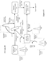
- FIG. 6A illustrates an exemplary DUV laser 600 configured to provide optimized bandwidth control.
- An optical parametric oscillator (OPO) or optical parametric amplifier (OPA) 604 is employed in the system.
- OPO optical parametric oscillator
- OPA optical parametric amplifier
- DUV laser 600 can generate output light at a chosen specific wavelength, i.e. a wavelength which may or may not be equal to an integer harmonic of the fundamental laser.
- the bandwidth of fundamental light 602 (generated by fundamental laser 601) can be narrowed by passing through an etalon 603 (see, e.g. arrows 611A and 611B).
- Etalon 603 preferably has high transmission over a narrow range of wavelengths centered close to the center wavelength of the fundamental light 602, so that the light transmitted through the etalon, narrowed fundamental 602', has a narrower bandwidth than the fundamental 602.
- Narrowed fundamental light 602' is directed to a harmonic conversion module 607, which generates an n th harmonic (n ⁇ ) 608, which is typically a DUV wavelength. Note that the n th harmonic 608 has a narrower bandwidth than would result from providing fundamental 602 to harmonic conversion module 607 directly.
- an out-of-band rejected fundamental 602" has a broad bandwidth with a dip in the middle of its spectrum.
- This rejected light 602 which would otherwise be wasted, can be used as a pump light for OPO/OPA 604.
- OPO/OPA 604 can still generate a narrow bandwidth signal light 605 from the broadband pump light of rejected fundamental 602" at the expense of generating a broad bandwidth idler light 606, which has a similar dip in the middle of its spectrum, but a broader bandwidth than rejected fundamental 602".
- the bandwidth of signal light 605 is determined by a seed laser or by a wavelength selective element, such as a volume-Bragg grating, in OPO/OPA 604.
- a Raman amplifier can replace OPO/OPA 604. Because the bandwidth of an amplified signal light generated by the Raman amplifier is independent of the bandwidth of its pump light (it typically depends on wavelength selective elements in the Raman amplifier), a Raman amplifier can also generate signal light 605 with a desired narrow bandwidth.
- a frequency mixing module 609 can generate a laser output 610 by summing the frequencies of the n th harmonic 608 (n ⁇ ) and the signal light 605 ( ⁇ s). Because the bandwidth of the n th harmonic 608 has been reduced by etalon 603 and the bandwidth of signal light 605 is determined by OPO/OPA 604, the bandwidth of laser output 610 is narrower than it would be in an otherwise identical laser that does not incorporate etalon 603 (that is, bandwidth indicated by arrow 611A would be used instead of bandwidth indicated by arrow 611B). This reduced bandwidth is achieved with minimal power losses since etalon 603 reflects most of the energy that it does not transmit.
- fundamental laser 601 may operate at a wavelength of approximately 1064 nm using, for example, a Nd:YAG (neodymium-doped yttrium aluminum garnet) or Nd-doped vanadate laser.
- harmonic conversion module 607 may generate a fifth harmonic 608 (5 ⁇ ) of approximately 213 nm
- OPO/OPA module 604 may generate signal light 605 having a wavelength of approximately 2108 nm
- frequency mixing module 609 may generate laser output 610 having a wavelength of approximately 193 nm by mixing the 213 nm and 2108 nm wavelengths.
- the wavelength of approximately 193 nm is a useful wavelength for inspecting semiconductor photomasks and wafers.
- the fundamental laser 601 may operate at a wavelength of approximately 1064 nm using, for example, a Nd:YAG or Nd-doped vandate laser.
- harmonic conversion module 607 may generate a fourth harmonic 608 (4 ⁇ ) of approximately 266 nm
- OPO/OPA module 604 may generate signal light 605 having a wavelength of approximately 1416 nm
- frequency mixing module 609 first mixes 266 nm and 1416 nm wavelengths to create a sum wavelength of approximately 224 nm, then remixes the sum wavelength of approximately 224 nm with the 1416 nm wavelength signal light 605 to generate a laser output 610 of wavelength approximately 193 nm.
- fundamental laser 601 may operate at a wavelength of approximately 1064 nm using, for example, a Nd:YAG (neodymium-doped yttrium aluminum garnet) or Nd-doped vanadate laser.
- harmonic conversion module 607 may generate a fifth harmonic 608 (5 ⁇ ) of approximately 213 nm
- OPO/OPA module 604 may generate signal light 605 having a wavelength of between approximately 1268 nm and approximately 1400 nm
- frequency mixing module 609 may generate laser output 610 having a wavelength of approximately 182.5 nm to approximately 185 nm by mixing the 213 nm and signal wavelengths.
- the wavelength of approximately 184 nm is a useful wavelength for inspecting semiconductor photomasks and wafers because short wavelengths generally have better sensitivity to smaller features and defects. Furthermore light of approximately 184 nm wavelength can be generated efficiently by this scheme because CLBO is close to non-critically phase matched for such wavelength combinations and so is efficient and stable for the frequency mixing.
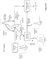
- FIG. 6B shows an alternate exemplary DUV laser 620 with optimized bandwidth control.
- the embodiment of DUV laser 620 is similar to that of DUV laser 600 ( Figure 6A ), except that DUV laser 620 does not include a harmonic conversion module.
- a frequency mixing module 609B generates a laser output 610B by directly mixing narrowed fundamental 602' and signal light 605.
- components in DUV lasers 620 and 600 having the same labels have the same functions and therefore are not be described in reference to Figure 6B .
- DUV laser 620 is particularly useful when fundamental laser 601 generates a UV wavelength, such as a wavelength of 405 nm or 375 nm. Such wavelengths can be generated, for example, by laser diodes.
- fundamental laser 601 may comprise a laser diode operating at a wavelength of approximately 375 nm.
- OPO/OPA module 604 may generate signal light 605 having a wavelength of between approximately 607 nm and approximately 750 nm
- frequency mixing module 609 may generate laser output 610 having a wavelength of between approximately 232 nm and approximately 250 nm by mixing the 375 nm and signal wavelengths.
- This scheme can efficiently and inexpensively generate the output wavelength of between approximately 232 nm and approximately 250 nm because frequency mixing module 609 may use a CLBO crystal for frequency mixing. CLBO is close to non-critically phase matched for such wavelength combinations and so can do the frequency mixing efficiently and stably.
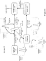
- FIG. 6C shows another exemplary DUV laser 630 with optimized bandwidth control.
- This embodiment of DUV laser 630 is similar to that of DUV laser 600 ( Figure 6A ), with the following exceptions.
- a harmonic conversion module 607C is used to generate an n th signal harmonic 608C (n ⁇ s) of signal light 605.
- a frequency mixing module 609C generates a laser output 610C by mixing narrowed fundamental 602' and n th signal harmonic 608C. Note that components in DUV lasers 630 and 600 having the same labels have the same functions and therefore are not be described in reference to Figure 6C .
- DUV 630 is particularly useful when the wavelength of laser output 610C cannot be achieved with a specific fundamental laser (for example, because the available non-linear crystals for frequency mixing module 609 or harmonic conversion module 607 (DUV laser 600, Figure 6A ) cannot phase match for one or more of the wavelengths).
- DUV laser 630 can provide different wavelength combinations for frequency mixing module 609C and harmonic conversion module 607C and can, in some cases, provide a viable way to generate the desired laser output wavelength when the embodiment of DUV 600 ( Figure 6A ) cannot.
- fundamental laser 601 may operate at a wavelength of approximately 800 nm using, for example, a Ti-sapphire laser.
- OPO/OPA module 604 may generate signal light 605 ( ⁇ s) having a wavelength between approximately 888 nm and 1080 nm
- harmonic conversion module 607 may generate a third harmonic 608 (3 ⁇ s) of between approximately 296 nm and 360 nm
- frequency mixing module 609 may generate laser output 610 having a wavelength of between approximately 216 nm and 248 nm by mixing the third harmonic and the approximately 800 nm wavelengths.
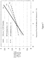
- FIG. 7 illustrates how pulse width shortening is possible by bandwidth filtering.
- Laser pulses generated by mode-locked or modulated laser oscillators usually have approximately Gaussian spectral shapes and exhibit approximately linear chirp.
- T0 is the transform-limited pulse width of a pulse with the same bandwidth as the chirped pulse;
- T is the pulse width before bandwidth reduction;
- T' is the pulse width after bandwidth reduction.
- a bandwidth reduction ratio is defined as the pulse bandwidth after filtering (i.e. after passing through the etalon) divided by the pulse bandwidth before filtering.
- Two cases of different bandwidth reduction ratios (0.6 and 0.8) are illustrated by dashed line 702 and dotted line 703 respectively.
- Figure 7 shows that under certain circumstances, bandwidth reduction of a chirped pulse would result in a shorter pulse, which is closer to transform-limited. For example, for the 0.6 bandwidth reduction ratio, when the pulse width T is greater than about 2 T0, reducing the bandwidth shortens the pulse width. In another example, for the 0.8 bandwidth reduction ratio, when the pulse width T is greater than about 1.6 T0, the pulse width is reduced when the bandwidth is reduced. As explained above, reducing the pulse width helps maintain the efficiency of the harmonic conversion and frequency mixing processes. Note that when the initial pulse width is close to T0, i.e. the initial pulse is close to transform limited, then any bandwidth reduction necessarily increases the pulse width.
- a typical high powered laser (such as a laser with an output of about 30W or more) has a pulse width significantly longer than a transform-limited pulse of the same bandwidth.
- the various methods and DUV lasers disclosed herein are particularly useful for generating narrow bandwidth DUV laser output light at powers of about 100 mW or more while maintaining good conversion efficiency.
- DUV lasers can be operated at other wavelengths shorter than about 200 nm by appropriate selection of the wavelength of the signal light ⁇ s and appropriate changes to the frequency mixing module (i.e. frequency mixing modules 609, 609B or 609C).
- frequency mixing module i.e. frequency mixing modules 609, 609B or 609C
- vacuum UV wavelengths shorter than 190 nm can be generated by such lasers.
- the harmonic conversion modules 607 of Figure 6A and 607C of Figure 6C might generate a second, third, fourth, fifth, sixth or higher harmonic.
- an etalon or interferometer may be designed to reflect a narrow range of wavelengths and transmit wavelengths outside that narrow range.
- Such an optical bandwidth filtering device could be substituted for the etalon 603 of Figures 6A , 6B and 6C with an appropriate change of the layout of the laser.
- the narrowed fundamental 602' would be reflected to harmonic conversion module 607, frequency mixing module 609 or frequency mixing module 609C as appropriate, and the rejected fundamental 602" would be transmitted to the frequency conversion module such as OPO/OPA 604.
Landscapes
- Physics & Mathematics (AREA)
- Nonlinear Science (AREA)
- General Physics & Mathematics (AREA)
- Electromagnetism (AREA)
- Optics & Photonics (AREA)
- Life Sciences & Earth Sciences (AREA)
- Chemical & Material Sciences (AREA)
- General Health & Medical Sciences (AREA)
- Pathology (AREA)
- Health & Medical Sciences (AREA)
- Immunology (AREA)
- Analytical Chemistry (AREA)
- Biochemistry (AREA)
- Engineering & Computer Science (AREA)
- Plasma & Fusion (AREA)
- Sustainable Development (AREA)
- Optical Modulation, Optical Deflection, Nonlinear Optics, Optical Demodulation, Optical Logic Elements (AREA)
- Investigating Materials By The Use Of Optical Means Adapted For Particular Applications (AREA)
- Testing Or Measuring Of Semiconductors Or The Like (AREA)
- Lasers (AREA)
Applications Claiming Priority (3)
| Application Number | Priority Date | Filing Date | Title |
|---|---|---|---|
| US201461955792P | 2014-03-20 | 2014-03-20 | |
| US14/300,227 US9804101B2 (en) | 2014-03-20 | 2014-06-09 | System and method for reducing the bandwidth of a laser and an inspection system and method using a laser |
| PCT/US2015/021462 WO2015143152A1 (en) | 2014-03-20 | 2015-03-19 | System and method for reducing the bandwidth of a laser and an inspection system and method using a laser |
Publications (3)
| Publication Number | Publication Date |
|---|---|
| EP3120427A1 EP3120427A1 (en) | 2017-01-25 |
| EP3120427A4 EP3120427A4 (en) | 2017-11-01 |
| EP3120427B1 true EP3120427B1 (en) | 2020-09-23 |
Family
ID=54141852
Family Applications (1)
| Application Number | Title | Priority Date | Filing Date |
|---|---|---|---|
| EP15765616.6A Active EP3120427B1 (en) | 2014-03-20 | 2015-03-19 | System and method for reducing the bandwidth of a laser and an inspection system and method using a laser |
Country Status (8)
| Country | Link |
|---|---|
| US (2) | US9804101B2 (enExample) |
| EP (1) | EP3120427B1 (enExample) |
| JP (1) | JP6529511B2 (enExample) |
| KR (1) | KR102220081B1 (enExample) |
| CN (1) | CN106134019B (enExample) |
| IL (2) | IL247580B (enExample) |
| TW (1) | TWI658662B (enExample) |
| WO (1) | WO2015143152A1 (enExample) |
Families Citing this family (24)
| Publication number | Priority date | Publication date | Assignee | Title |
|---|---|---|---|---|
| US8873596B2 (en) | 2011-07-22 | 2014-10-28 | Kla-Tencor Corporation | Laser with high quality, stable output beam, and long life high conversion efficiency non-linear crystal |
| US9478402B2 (en) | 2013-04-01 | 2016-10-25 | Kla-Tencor Corporation | Photomultiplier tube, image sensor, and an inspection system using a PMT or image sensor |
| US12130141B2 (en) * | 2013-05-14 | 2024-10-29 | The Charles Stark Draper Laboratory, Inc. | Star tracker with adjustable light shield |
| US9410901B2 (en) | 2014-03-17 | 2016-08-09 | Kla-Tencor Corporation | Image sensor, an inspection system and a method of inspecting an article |
| US9726897B2 (en) | 2014-05-28 | 2017-08-08 | Motex, Inc. | Cube polarizer with minimal optical path length difference |
| US10268046B2 (en) | 2014-05-28 | 2019-04-23 | Moxtek, Inc. | Cube polarizer |
| US9419407B2 (en) | 2014-09-25 | 2016-08-16 | Kla-Tencor Corporation | Laser assembly and inspection system using monolithic bandwidth narrowing apparatus |
| US9748729B2 (en) | 2014-10-03 | 2017-08-29 | Kla-Tencor Corporation | 183NM laser and inspection system |
| US20160231487A1 (en) * | 2015-02-06 | 2016-08-11 | Moxtek, Inc. | High Contrast Inverse Polarizer |
| US10234613B2 (en) | 2015-02-06 | 2019-03-19 | Moxtek, Inc. | High contrast inverse polarizer |
| CN104759753B (zh) * | 2015-03-30 | 2016-08-31 | 江苏大学 | 多系统自动化协调工作提高激光诱导空化强化的方法 |
| US10748730B2 (en) | 2015-05-21 | 2020-08-18 | Kla-Tencor Corporation | Photocathode including field emitter array on a silicon substrate with boron layer |
| US9785050B2 (en) | 2015-06-26 | 2017-10-10 | Cymer, Llc | Pulsed light beam spectral feature control |
| US10783624B2 (en) * | 2016-07-18 | 2020-09-22 | Instrumental, Inc. | Modular optical inspection station |
| JP6306659B1 (ja) * | 2016-10-19 | 2018-04-04 | ファナック株式会社 | ビーム分配器 |
| US10175555B2 (en) | 2017-01-03 | 2019-01-08 | KLA—Tencor Corporation | 183 nm CW laser and inspection system |
| US10551320B2 (en) * | 2017-01-30 | 2020-02-04 | Kla-Tencor Corporation | Activation of wafer particle defects for spectroscopic composition analysis |
| US10409139B2 (en) | 2017-09-21 | 2019-09-10 | Qioptiq Photonics Gmbh & Co. Kg | Light source with multi-longitudinal mode continuous wave output based on multi-mode resonant OPO technology |
| US10756505B2 (en) | 2017-09-21 | 2020-08-25 | Qioptiq Photonics Gmbh & Co. Kg | Tunable light source with broadband output |
| US10943760B2 (en) | 2018-10-12 | 2021-03-09 | Kla Corporation | Electron gun and electron microscope |
| US10921261B2 (en) * | 2019-05-09 | 2021-02-16 | Kla Corporation | Strontium tetraborate as optical coating material |
| JP7679365B2 (ja) * | 2019-11-07 | 2025-05-19 | サイマー リミテッド ライアビリティ カンパニー | 光源によって生成される出力光ビームの分光特性の制御 |
| CN110987965B (zh) * | 2019-12-26 | 2023-03-31 | 中国科学院微电子研究所 | 基于非相干光源和波带片成像的掩模缺陷检测方法及系统 |
| US12379642B2 (en) * | 2021-06-11 | 2025-08-05 | Kla Corporation | Tunable DUV laser assembly |
Family Cites Families (211)
| Publication number | Priority date | Publication date | Assignee | Title |
|---|---|---|---|---|
| US3755704A (en) | 1970-02-06 | 1973-08-28 | Stanford Research Inst | Field emission cathode structures and devices utilizing such structures |
| US4178561A (en) | 1978-10-02 | 1979-12-11 | Hughes Aircraft Company | Scanning arrangements for optical frequency converters |
| JPS58146B2 (ja) | 1980-10-14 | 1983-01-05 | 浜松テレビ株式会社 | フレ−ミング管 |
| US4644221A (en) | 1981-05-06 | 1987-02-17 | The United States Of America As Represented By The Secretary Of The Army | Variable sensitivity transmission mode negative electron affinity photocathode |
| US4710030A (en) | 1985-05-17 | 1987-12-01 | Bw Brown University Research Foundation | Optical generator and detector of stress pulses |
| US4853595A (en) | 1987-08-31 | 1989-08-01 | Alfano Robert R | Photomultiplier tube having a transmission strip line photocathode and system for use therewith |
| US4999014A (en) | 1989-05-04 | 1991-03-12 | Therma-Wave, Inc. | Method and apparatus for measuring thickness of thin films |
| CN1021269C (zh) | 1990-10-11 | 1993-06-16 | 中国科学院上海光学精密机械研究所 | 内腔式高次谐波激光器 |
| US5120949A (en) | 1991-01-17 | 1992-06-09 | Burle Technologies, Inc. | Semiconductor anode photomultiplier tube |
| JP2828221B2 (ja) | 1991-06-04 | 1998-11-25 | インターナショナル・ビジネス・マシーンズ・コーポレイション | レーザー光波長変換装置 |
| US5189481A (en) | 1991-07-26 | 1993-02-23 | Tencor Instruments | Particle detector for rough surfaces |
| US5144630A (en) | 1991-07-29 | 1992-09-01 | Jtt International, Inc. | Multiwavelength solid state laser using frequency conversion techniques |
| US5563702A (en) | 1991-08-22 | 1996-10-08 | Kla Instruments Corporation | Automated photomask inspection apparatus and method |
| DE69208413T2 (de) | 1991-08-22 | 1996-11-14 | Kla Instr Corp | Gerät zur automatischen Prüfung von Photomaske |
| EP0532927B1 (en) | 1991-08-22 | 1996-02-21 | Kla Instruments Corporation | Automated photomask inspection apparatus |
| US5475227A (en) | 1992-12-17 | 1995-12-12 | Intevac, Inc. | Hybrid photomultiplier tube with ion deflector |
| US5326978A (en) | 1992-12-17 | 1994-07-05 | Intevac, Inc. | Focused electron-bombarded detector |
| US5760809A (en) | 1993-03-19 | 1998-06-02 | Xerox Corporation | Recording sheets containing phosphonium compounds |
| FI940740A0 (fi) | 1994-02-17 | 1994-02-17 | Arto Salokatve | Detektor foer paovisning av fotoner eller partiklar, foerfarande foer framstaellning av detektorn och maetningsfoerfarande |
| US6271916B1 (en) | 1994-03-24 | 2001-08-07 | Kla-Tencor Corporation | Process and assembly for non-destructive surface inspections |
| US5493176A (en) | 1994-05-23 | 1996-02-20 | Siemens Medical Systems, Inc. | Photomultiplier tube with an avalanche photodiode, a flat input end and conductors which simulate the potential distribution in a photomultiplier tube having a spherical-type input end |
| US6512631B2 (en) | 1996-07-22 | 2003-01-28 | Kla-Tencor Corporation | Broad-band deep ultraviolet/vacuum ultraviolet catadioptric imaging system |
| US5741626A (en) | 1996-04-15 | 1998-04-21 | Motorola, Inc. | Method for forming a dielectric tantalum nitride layer as an anti-reflective coating (ARC) |
| WO1997046865A1 (en) | 1996-06-04 | 1997-12-11 | Tencor Instruments | Optical scanning system for surface inspection |
| US5999310A (en) | 1996-07-22 | 1999-12-07 | Shafer; David Ross | Ultra-broadband UV microscope imaging system with wide range zoom capability |
| US5742626A (en) * | 1996-08-14 | 1998-04-21 | Aculight Corporation | Ultraviolet solid state laser, method of using same and laser surgery apparatus |
| US5760899A (en) | 1996-09-04 | 1998-06-02 | Erim International, Inc. | High-sensitivity multispectral sensor |
| US6201257B1 (en) | 1996-10-10 | 2001-03-13 | Advanced Scientific Concepts, Inc. | Semiconductor X-ray photocathodes devices |
| US6212310B1 (en) | 1996-10-22 | 2001-04-03 | Sdl, Inc. | High power fiber gain media system achieved through power scaling via multiplexing |
| US6064759A (en) | 1996-11-08 | 2000-05-16 | Buckley; B. Shawn | Computer aided inspection machine |
| US5898717A (en) * | 1997-01-24 | 1999-04-27 | Photonics Industries International, Inc. | Third harmonic generation apparatus |
| EP1658663A4 (en) | 1997-03-21 | 2009-11-11 | Imra America Inc | FIBER OPTIC HIGH ENERGY AMPLIFIER FOR PICOSCIENCE NANOSECUSTOMER IMPULSES FOR ADVANCED MATERIAL PROCESSING APPLICATIONS |
| US6608676B1 (en) | 1997-08-01 | 2003-08-19 | Kla-Tencor Corporation | System for detecting anomalies and/or features of a surface |
| US5825562A (en) | 1997-08-18 | 1998-10-20 | Novatec Corporation | Method of continuous motion for prolong usage of optical elements under the irradiation of intensive laser beams |
| US6201601B1 (en) | 1997-09-19 | 2001-03-13 | Kla-Tencor Corporation | Sample inspection system |
| JPH11121854A (ja) | 1997-10-16 | 1999-04-30 | Ushio Sogo Gijutsu Kenkyusho:Kk | 光源装置 |
| KR100819239B1 (ko) | 1998-03-11 | 2008-04-03 | 가부시키가이샤 니콘 | 자외 레이저 장치, 레이저 장치, 노광 장치와 노광 방법, 디바이스 제조 방법, 자외광 조사 장치, 물체 패턴 검출 장치, 자외광 조사 방법 및 물체 패턴 검출 방법 |
| JP3997450B2 (ja) | 1998-03-13 | 2007-10-24 | ソニー株式会社 | 波長変換装置 |
| US6376985B2 (en) | 1998-03-31 | 2002-04-23 | Applied Materials, Inc. | Gated photocathode for controlled single and multiple electron beam emission |
| US6373869B1 (en) | 1998-07-30 | 2002-04-16 | Actinix | System and method for generating coherent radiation at ultraviolet wavelengths |
| US6067311A (en) | 1998-09-04 | 2000-05-23 | Cymer, Inc. | Excimer laser with pulse multiplier |
| KR20000034461A (ko) | 1998-11-30 | 2000-06-26 | 전주범 | 펄스발생장치 |
| US6184984B1 (en) | 1999-02-09 | 2001-02-06 | Kla-Tencor Corporation | System for measuring polarimetric spectrum and other properties of a sample |
| ATE246367T1 (de) | 1999-06-11 | 2003-08-15 | Daniel Dr Kopf | Laser-generatorsystem |
| US6888855B1 (en) | 1999-06-11 | 2005-05-03 | Daniel Kopf | Optical system for lasers |
| US6285018B1 (en) | 1999-07-20 | 2001-09-04 | Intevac, Inc. | Electron bombarded active pixel sensor |
| JP2001042369A (ja) | 1999-07-27 | 2001-02-16 | Ushio Sogo Gijutsu Kenkyusho:Kk | 波長変換ユニット |
| US6498801B1 (en) | 1999-08-05 | 2002-12-24 | Alexander E. Dudelzak | Solid state laser for microlithography |
| US7136402B1 (en) | 1999-09-10 | 2006-11-14 | Nikon Corporation | Laser device and exposure method |
| EP1139521A4 (en) | 1999-09-10 | 2006-03-22 | Nikon Corp | LIGHT SOURCE AND WAVELENGTH STABILIZATION CONTROL METHOD, EXPOSURE APPARATUS AND METHOD, METHOD FOR PRODUCING EXPOSURE APPARATUS, AND DEVICE MANUFACTURING METHOD, AND DEVICE THEREOF |
| AU2723601A (en) | 1999-09-23 | 2001-05-10 | Purdue Research Foundation | Direct space-to-time pulse shaper and optical pulse train generator |
| US6369888B1 (en) | 1999-11-17 | 2002-04-09 | Applied Materials, Inc. | Method and apparatus for article inspection including speckle reduction |
| US7838794B2 (en) | 1999-12-28 | 2010-11-23 | Gsi Group Corporation | Laser-based method and system for removing one or more target link structures |
| US6549647B1 (en) | 2000-01-07 | 2003-04-15 | Cyberoptics Corporation | Inspection system with vibration resistant video capture |
| US6879390B1 (en) | 2000-08-10 | 2005-04-12 | Kla-Tencor Technologies Corporation | Multiple beam inspection apparatus and method |
| JP2002055368A (ja) | 2000-08-11 | 2002-02-20 | Takano Co Ltd | 波長変換レーザ装置 |
| US7136159B2 (en) | 2000-09-12 | 2006-11-14 | Kla-Tencor Technologies Corporation | Excimer laser inspection system |
| US7184616B2 (en) | 2000-11-20 | 2007-02-27 | Aculight Corporation | Method and apparatus for fiber Bragg grating production |
| US6693930B1 (en) | 2000-12-12 | 2004-02-17 | Kla-Tencor Technologies Corporation | Peak power and speckle contrast reduction for a single laser pulse |
| US6704339B2 (en) | 2001-01-29 | 2004-03-09 | Cymer, Inc. | Lithography laser with beam delivery and beam pointing control |
| US8208505B2 (en) | 2001-01-30 | 2012-06-26 | Board Of Trustees Of Michigan State University | Laser system employing harmonic generation |
| US6791099B2 (en) | 2001-02-14 | 2004-09-14 | Applied Materials, Inc. | Laser scanning wafer inspection using nonlinear optical phenomena |
| JP3939928B2 (ja) | 2001-02-28 | 2007-07-04 | サイバーレーザー株式会社 | 波長変換装置 |
| JP2003043533A (ja) | 2001-08-03 | 2003-02-13 | Kitakyushu Foundation For The Advancement Of Industry Science & Technology | レーザーの第二高調波の方向を一定に保つための自動追尾装置 |
| US6678046B2 (en) | 2001-08-28 | 2004-01-13 | Therma-Wave, Inc. | Detector configurations for optical metrology |
| US20060126682A1 (en) | 2001-10-08 | 2006-06-15 | Geola Technologies Ltd. | Pulsed multiple colour laser system |
| US20030161374A1 (en) | 2001-11-21 | 2003-08-28 | Lambda Physik Ag | High-resolution confocal Fabry-Perot interferometer for absolute spectral parameter detection of excimer laser used in lithography applications |
| US6816520B1 (en) | 2001-11-30 | 2004-11-09 | Positive Light | Solid state system and method for generating ultraviolet light |
| US7088443B2 (en) | 2002-02-11 | 2006-08-08 | Kla-Tencor Technologies Corporation | System for detecting anomalies and/or features of a surface |
| US6859335B1 (en) | 2002-11-20 | 2005-02-22 | Ming Lai | Method of programmed displacement for prolong usage of optical elements under the irradiation of intensive laser beams |
| GB2398118B (en) | 2003-02-07 | 2006-03-15 | Imp College Innovations Ltd | Photon arrival time detection |
| US7957066B2 (en) | 2003-02-21 | 2011-06-07 | Kla-Tencor Corporation | Split field inspection system using small catadioptric objectives |
| EP1666520B1 (en) | 2003-09-11 | 2013-11-13 | Nikon Corporation | A macromolecular crystral working apparatus ; A macromolecular crystal evaluating device with such apparatus |
| US7463657B2 (en) | 2003-10-09 | 2008-12-09 | Coherent, Inc. | Intracavity frequency-tripled CW laser |
| US7813406B1 (en) | 2003-10-15 | 2010-10-12 | The United States Of America As Represented By The Administrator Of The National Aeronautics And Space Administration | Temporal laser pulse manipulation using multiple optical ring-cavities |
| JP2005156516A (ja) | 2003-11-05 | 2005-06-16 | Hitachi Ltd | パターン欠陥検査方法及びその装置 |
| US7023126B2 (en) | 2003-12-03 | 2006-04-04 | Itt Manufacturing Enterprises Inc. | Surface structures for halo reduction in electron bombarded devices |
| US20050157382A1 (en) | 2004-01-07 | 2005-07-21 | Kafka James D. | Industrial directly diode-pumped ultrafast amplifier system |
| US7313155B1 (en) | 2004-02-12 | 2007-12-25 | Liyue Mu | High power Q-switched laser for soft tissue ablation |
| US7035012B2 (en) | 2004-03-01 | 2006-04-25 | Coherent, Inc. | Optical pulse duration extender |
| JPWO2005085947A1 (ja) | 2004-03-08 | 2008-01-24 | 株式会社ニコン | レーザ光源装置、このレーザ光源装置を用いた露光装置及びマスク検査装置 |
| JP4365255B2 (ja) | 2004-04-08 | 2009-11-18 | 浜松ホトニクス株式会社 | 発光体と、これを用いた電子線検出器、走査型電子顕微鏡及び質量分析装置 |
| US20050254065A1 (en) | 2004-05-12 | 2005-11-17 | Stokowski Stanley E | Method and apparatus for detecting surface characteristics on a mask blank |
| US7349079B2 (en) | 2004-05-14 | 2008-03-25 | Kla-Tencor Technologies Corp. | Methods for measurement or analysis of a nitrogen concentration of a specimen |
| JP4636020B2 (ja) | 2004-05-26 | 2011-02-23 | 株式会社ニコン | 波長変換光学系、レーザ光源、露光装置、マスク検査装置、及び高分子結晶の加工装置 |
| JP2006060162A (ja) | 2004-08-24 | 2006-03-02 | Nikon Corp | レーザ光源装置の励起光の制御方法及びレーザ光源装置 |
| US7627007B1 (en) | 2004-08-25 | 2009-12-01 | Kla-Tencor Technologies Corporation | Non-critical phase matching in CLBO to generate sub-213nm wavelengths |
| JP4500641B2 (ja) | 2004-09-29 | 2010-07-14 | 株式会社日立ハイテクノロジーズ | 欠陥検査方法およびその装置 |
| US7952633B2 (en) | 2004-11-18 | 2011-05-31 | Kla-Tencor Technologies Corporation | Apparatus for continuous clocking of TDI sensors |
| US7609309B2 (en) | 2004-11-18 | 2009-10-27 | Kla-Tencor Technologies Corporation | Continuous clocking of TDI sensors |
| JP4627185B2 (ja) | 2004-12-27 | 2011-02-09 | 株式会社小松製作所 | 光学パルスストレッチ装置における遅延光学路長の設定方法 |
| US7528342B2 (en) | 2005-02-03 | 2009-05-05 | Laserfacturing, Inc. | Method and apparatus for via drilling and selective material removal using an ultrafast pulse laser |
| JP2006250845A (ja) | 2005-03-14 | 2006-09-21 | Topcon Corp | パターン欠陥検査方法とその装置 |
| US7593440B2 (en) | 2005-03-29 | 2009-09-22 | Coherent, Inc. | MOPA laser apparatus with two master oscillators for generating ultraviolet radiation |
| DE602006004913D1 (de) | 2005-04-28 | 2009-03-12 | Semiconductor Energy Lab | Verfahren und Vorrichtung zur Herstellung von Halbleitern mittels Laserstrahlung |
| EP1734584A1 (en) | 2005-06-14 | 2006-12-20 | Photonis-DEP B.V. | Electron bombarded image sensor array device as well as such an image sensor array |
| US7345825B2 (en) | 2005-06-30 | 2008-03-18 | Kla-Tencor Technologies Corporation | Beam delivery system for laser dark-field illumination in a catadioptric optical system |
| JP4640029B2 (ja) | 2005-08-08 | 2011-03-02 | 株式会社ニコン | 波長変換光学系、レーザ光源、露光装置、被検物検査装置、及び高分子結晶の加工装置 |
| US7535938B2 (en) | 2005-08-15 | 2009-05-19 | Pavilion Integration Corporation | Low-noise monolithic microchip lasers capable of producing wavelengths ranging from IR to UV based on efficient and cost-effective frequency conversion |
| US7864425B2 (en) | 2005-09-16 | 2011-01-04 | Panasonic Corporation | Composite material and optical component using the same |
| JP4925085B2 (ja) | 2005-09-20 | 2012-04-25 | 株式会社メガオプト | 深紫外レーザー光の発生方法および深紫外レーザー装置 |
| FR2892854A1 (fr) * | 2005-10-27 | 2007-05-04 | Sidel Sas | Methode de surveillance d'un plasma, dispositif pour la mise en oeuvre de cette methode, application de cette methode au depot d'un film sur corps creux en pet |
| JP4939033B2 (ja) | 2005-10-31 | 2012-05-23 | 浜松ホトニクス株式会社 | 光電陰極 |
| KR101194231B1 (ko) | 2005-11-01 | 2012-10-29 | 사이머 인코포레이티드 | 레이저 시스템 |
| US7920616B2 (en) | 2005-11-01 | 2011-04-05 | Cymer, Inc. | Laser system |
| US7885309B2 (en) | 2005-11-01 | 2011-02-08 | Cymer, Inc. | Laser system |
| US20090296755A1 (en) | 2005-11-01 | 2009-12-03 | Cymer, Inc. | Laser system |
| US7715459B2 (en) | 2005-11-01 | 2010-05-11 | Cymer, Inc. | Laser system |
| US7643529B2 (en) | 2005-11-01 | 2010-01-05 | Cymer, Inc. | Laser system |
| JP2007133102A (ja) | 2005-11-09 | 2007-05-31 | Canon Inc | 反射防止膜を有する光学素子及びそれを有する露光装置 |
| US7471705B2 (en) | 2005-11-09 | 2008-12-30 | Lockheed Martin Corporation | Ultraviolet laser system and method having wavelength in the 200-nm range |
| US7519253B2 (en) | 2005-11-18 | 2009-04-14 | Omni Sciences, Inc. | Broadband or mid-infrared fiber light sources |
| US7528943B2 (en) | 2005-12-27 | 2009-05-05 | Kla-Tencor Technologies Corporation | Method and apparatus for simultaneous high-speed acquisition of multiple images |
| JP2007206452A (ja) | 2006-02-02 | 2007-08-16 | Lasertec Corp | 深紫外光源及び、その深紫外光源を用いたマスク検査装置及び露光装置 |
| JP4911494B2 (ja) | 2006-03-18 | 2012-04-04 | 国立大学法人大阪大学 | 波長変換光学素子、波長変換光学素子の製造方法、波長変換装置、紫外線レーザ照射装置およびレーザ加工装置 |
| EP2013951A4 (en) | 2006-04-28 | 2011-08-03 | Corning Inc | PULSED RAMAN LASER SYSTEMS IN ULTRAVIOLET AND VISIBLE LIGHT |
| US7113325B1 (en) | 2006-05-03 | 2006-09-26 | Mitsubishi Materials Corporation | Wavelength conversion method with improved conversion efficiency |
| US20070263680A1 (en) | 2006-05-15 | 2007-11-15 | Andrei Starodoumov | MOPA laser apparatus with two master oscillators for generating ultraviolet radiation |
| US7593437B2 (en) | 2006-05-15 | 2009-09-22 | Coherent, Inc. | MOPA laser apparatus with two master oscillators for generating ultraviolet radiation |
| US20090185583A1 (en) | 2006-06-02 | 2009-07-23 | Corning Incorporated | UV and Visible Laser Systems |
| US7457330B2 (en) | 2006-06-15 | 2008-11-25 | Pavilion Integration Corporation | Low speckle noise monolithic microchip RGB lasers |
| CN100426117C (zh) * | 2006-06-22 | 2008-10-15 | 天津大学 | 全光纤窄带宽单光子源 |
| US7970201B2 (en) | 2006-07-31 | 2011-06-28 | Applied Materials Israel, Ltd. | Method and system for defect detection |
| CN100530070C (zh) | 2006-11-24 | 2009-08-19 | 骆建军 | 基于flash的硬盘 |
| DE102007004235B3 (de) | 2006-12-21 | 2008-01-03 | Coherent Gmbh | Verfahren zur Frequenzkonversion eines Lichtstrahls mittels eines CLBO-Kristalls |
| JP5342769B2 (ja) | 2006-12-28 | 2013-11-13 | 浜松ホトニクス株式会社 | 光電陰極、電子管及び光電子増倍管 |
| US9771666B2 (en) | 2007-01-17 | 2017-09-26 | Crystal Is, Inc. | Defect reduction in seeded aluminum nitride crystal growth |
| WO2008088838A1 (en) | 2007-01-17 | 2008-07-24 | Crystal Is, Inc. | Defect reduction in seeded aluminum nitride crystal growth |
| JP4224863B2 (ja) | 2007-02-02 | 2009-02-18 | レーザーテック株式会社 | 検査装置及び検査方法、並びにパターン基板の製造方法 |
| JP2008209664A (ja) | 2007-02-27 | 2008-09-11 | Advanced Mask Inspection Technology Kk | パターン検査装置 |
| JP2008261790A (ja) | 2007-04-13 | 2008-10-30 | Hitachi High-Technologies Corp | 欠陥検査装置 |
| US8755417B1 (en) | 2007-04-16 | 2014-06-17 | Kla-Tencor Corporation | Coherent light generation below about two-hundred nanometers |
| US20110073982A1 (en) | 2007-05-25 | 2011-03-31 | Armstrong J Joseph | Inspection system using back side illuminated linear sensor |
| US7586108B2 (en) | 2007-06-25 | 2009-09-08 | Asml Netherlands B.V. | Radiation detector, method of manufacturing a radiation detector and lithographic apparatus comprising a radiation detector |
| US7782913B2 (en) * | 2007-07-20 | 2010-08-24 | Corning Incorporated | Intensity modulation in wavelength converting optical package |
| US7999342B2 (en) | 2007-09-24 | 2011-08-16 | Taiwan Semiconductor Manufacturing Company, Ltd | Image sensor element for backside-illuminated sensor |
| JP4634427B2 (ja) | 2007-09-27 | 2011-02-16 | 株式会社東芝 | 照明装置及びパターン検査装置 |
| US7525649B1 (en) | 2007-10-19 | 2009-04-28 | Kla-Tencor Technologies Corporation | Surface inspection system using laser line illumination with two dimensional imaging |
| US7605376B2 (en) | 2007-10-29 | 2009-10-20 | Fairchild Imaging, Inc. | CMOS sensor adapted for dental x-ray imaging |
| US8298335B2 (en) | 2007-12-18 | 2012-10-30 | Kla-Tencor Technologies Corporation | Enclosure for controlling the environment of optical crystals |
| JP2009145791A (ja) | 2007-12-18 | 2009-07-02 | Lasertec Corp | 波長変換装置、検査装置及び波長変換方法 |
| US7885298B2 (en) | 2008-01-16 | 2011-02-08 | Deep Photonics Corporation | Method and apparatus for producing arbitrary pulsetrains from a harmonic fiber laser |
| JP5305377B2 (ja) * | 2008-06-26 | 2013-10-02 | 株式会社フジクラ | ラマン光増幅を用いた光伝送システム |
| JP2010054547A (ja) | 2008-08-26 | 2010-03-11 | Lasertec Corp | 紫外レーザ装置 |
| KR101036879B1 (ko) | 2008-08-27 | 2011-05-25 | 주식회사 이오테크닉스 | 드릴링 장치 및 드릴링 방법 |
| KR101661090B1 (ko) | 2008-09-29 | 2016-09-28 | 케이엘에이-텐코어 코오포레이션 | 계측 시스템의 조명 서브시스템들, 계측 시스템들 및 계측 측정들을 위한 표본을 조명하기 위한 방법들 |
| US9080991B2 (en) | 2008-09-29 | 2015-07-14 | Kla-Tencor Corp. | Illuminating a specimen for metrology or inspection |
| US7875948B2 (en) | 2008-10-21 | 2011-01-25 | Jaroslav Hynecek | Backside illuminated image sensor |
| FR2938935B1 (fr) | 2008-11-21 | 2011-05-06 | Eolite Systems | Dispositif d'allongement de la duree de vie d'un systeme optique non lineaire soumis au rayonnement d'un faisceau laser intense et source optique non lineaire comprenant ce dispositif |
| US8146498B2 (en) | 2008-12-03 | 2012-04-03 | Eastman Kodak Company | Printing plate registration |
| US8017427B2 (en) | 2008-12-31 | 2011-09-13 | Omnivision Technologies, Inc. | Backside-illuminated (BSI) image sensor with backside diffusion doping |
| US8624971B2 (en) | 2009-01-23 | 2014-01-07 | Kla-Tencor Corporation | TDI sensor modules with localized driving and signal processing circuitry for high speed inspection |
| KR20100103238A (ko) | 2009-03-13 | 2010-09-27 | 삼성전자주식회사 | 에피 웨이퍼 제조 방법 및 그에 의해 제조된 에피 웨이퍼, 및 상기 에피 웨이퍼로 제조한 이미지 센서 |
| JP5237874B2 (ja) | 2009-04-24 | 2013-07-17 | 株式会社日立ハイテクノロジーズ | 欠陥検査方法および欠陥検査装置 |
| JP4565207B1 (ja) | 2009-04-28 | 2010-10-20 | レーザーテック株式会社 | 波長変換装置及び波長変換方法並びに半導体装置の製造方法 |
| US20100301437A1 (en) | 2009-06-01 | 2010-12-02 | Kla-Tencor Corporation | Anti-Reflective Coating For Sensors Suitable For High Throughput Inspection Systems |
| JP2011023532A (ja) | 2009-07-15 | 2011-02-03 | Nikon Corp | 光増幅器、レーザ装置及び光源装置 |
| US9023152B2 (en) | 2009-09-17 | 2015-05-05 | Kla-Tencor Corporation | CLBO crystal growth |
| CN102035085B (zh) | 2009-10-08 | 2014-03-05 | 群康科技(深圳)有限公司 | 导电结构及其制造方法 |
| WO2011046780A1 (en) | 2009-10-13 | 2011-04-21 | Nanda Nathan | Pulsed high-power laser apparatus and methods |
| US8629384B1 (en) | 2009-10-26 | 2014-01-14 | Kla-Tencor Corporation | Photomultiplier tube optimized for surface inspection in the ultraviolet |
| CN101702490B (zh) | 2009-10-29 | 2011-02-09 | 长春理工大学 | 一种采用阱中量子点(dwell)的中红外锑化物激光器结构 |
| DE102009047098A1 (de) | 2009-11-25 | 2011-05-26 | Carl Zeiss Smt Gmbh | Optische Anordnung zur Homogenisierung eines Laserpulses |
| US20110134944A1 (en) | 2009-12-08 | 2011-06-09 | The Arizona Board Of Regents On Behalf Of The University Of Arizona | Efficient pulse laser light generation and devices using the same |
| JP2011128330A (ja) | 2009-12-17 | 2011-06-30 | Nikon Corp | レーザ装置 |
| JP5455044B2 (ja) * | 2010-02-02 | 2014-03-26 | 株式会社ニコン | レーザ装置 |
| JP4590578B1 (ja) | 2010-04-01 | 2010-12-01 | レーザーテック株式会社 | 光源装置、マスク検査装置、及びコヒーレント光発生方法 |
| WO2011148895A1 (ja) | 2010-05-24 | 2011-12-01 | ギガフォトン株式会社 | 固体レーザ装置およびレーザシステム |
| EP2601714A4 (en) | 2010-08-08 | 2014-12-17 | Kla Tencor Corp | DYNAMIC WAVE FRONT CONTROL OF A LASER SYSTEM WITH FREQUENCY CONVERSION |
| US8482846B2 (en) | 2010-08-09 | 2013-07-09 | Coherent Gmbh | Advanced shifting algorithm for prolonging the life of an optically nonlinear crystal |
| JP5568444B2 (ja) | 2010-11-01 | 2014-08-06 | 株式会社日立ハイテクノロジーズ | 欠陥検査方法、微弱光検出方法および微弱光検出器 |
| US8824514B2 (en) | 2010-11-09 | 2014-09-02 | Kla-Tencor Corporation | Measuring crystal site lifetime in a non-linear optical crystal |
| US8711470B2 (en) | 2010-11-14 | 2014-04-29 | Kla-Tencor Corporation | High damage threshold frequency conversion system |
| SG10201510329VA (en) | 2010-12-16 | 2016-01-28 | Kla Tencor Corp | Wafer inspection |
| US8669512B2 (en) | 2010-12-28 | 2014-03-11 | Technion Research & Development Foundation Limited | System and method for analyzing light by three-photon counting |
| WO2012154468A2 (en) | 2011-05-06 | 2012-11-15 | Kla-Tencor Corporation | Deep ultra-violet light sources for wafer and reticle inspection systems |
| US9793673B2 (en) | 2011-06-13 | 2017-10-17 | Kla-Tencor Corporation | Semiconductor inspection and metrology system using laser pulse multiplier |
| US9920438B2 (en) | 2011-07-07 | 2018-03-20 | Massachusetts Institute Of Technology | Methods and apparatus for ultrathin catalyst layer for photoelectrode |
| JP5731444B2 (ja) | 2011-07-07 | 2015-06-10 | 富士フイルム株式会社 | 放射線検出器、放射線画像撮影装置、及び放射線画像撮影システム |
| US9279774B2 (en) | 2011-07-12 | 2016-03-08 | Kla-Tencor Corp. | Wafer inspection |
| ITTO20110649A1 (it) | 2011-07-19 | 2013-01-20 | St Microelectronics Srl | Dispositivo di fotorivelazione con copertura protettiva e antiriflesso, e relativo metodo di fabbricazione |
| US8873596B2 (en) | 2011-07-22 | 2014-10-28 | Kla-Tencor Corporation | Laser with high quality, stable output beam, and long life high conversion efficiency non-linear crystal |
| CN102901616B (zh) * | 2011-07-28 | 2015-05-20 | 中国计量科学研究院 | 一种激光线宽测量方法和设备 |
| US8817827B2 (en) | 2011-08-17 | 2014-08-26 | Veralas, Inc. | Ultraviolet fiber laser system |
| WO2013036576A1 (en) | 2011-09-07 | 2013-03-14 | Kla-Tencor Corporation | Transmissive-reflective photocathode |
| US8748828B2 (en) | 2011-09-21 | 2014-06-10 | Kla-Tencor Corporation | Interposer based imaging sensor for high-speed image acquisition and inspection systems |
| US20130077086A1 (en) | 2011-09-23 | 2013-03-28 | Kla-Tencor Corporation | Solid-State Laser And Inspection System Using 193nm Laser |
| US8872159B2 (en) | 2011-09-29 | 2014-10-28 | The United States Of America, As Represented By The Secretary Of The Navy | Graphene on semiconductor detector |
| US9250178B2 (en) | 2011-10-07 | 2016-02-02 | Kla-Tencor Corporation | Passivation of nonlinear optical crystals |
| US9389166B2 (en) | 2011-12-16 | 2016-07-12 | Kla-Tencor Corporation | Enhanced high-speed logarithmic photo-detector for spot scanning system |
| US8754972B2 (en) | 2012-02-01 | 2014-06-17 | Kla-Tencor Corporation | Integrated multi-channel analog front end and digitizer for high speed imaging applications |
| US9496425B2 (en) | 2012-04-10 | 2016-11-15 | Kla-Tencor Corporation | Back-illuminated sensor with boron layer |
| US20130313440A1 (en) | 2012-05-22 | 2013-11-28 | Kla-Tencor Corporation | Solid-State Laser And Inspection System Using 193nm Laser |
| US8953869B2 (en) | 2012-06-14 | 2015-02-10 | Kla-Tencor Corporation | Apparatus and methods for inspecting extreme ultra violet reticles |
| US8964798B2 (en) | 2012-07-12 | 2015-02-24 | Kla-Tencor Corporation | Reducing the spectral bandwidth of lasers |
| US9601299B2 (en) | 2012-08-03 | 2017-03-21 | Kla-Tencor Corporation | Photocathode including silicon substrate with boron layer |
| US9042006B2 (en) | 2012-09-11 | 2015-05-26 | Kla-Tencor Corporation | Solid state illumination source and inspection system |
| NL2011568A (en) | 2012-10-31 | 2014-05-06 | Asml Netherlands Bv | Sensor and lithographic apparatus. |
| US9147992B2 (en) | 2012-11-09 | 2015-09-29 | Coherent, Inc. | High efficiency amplification of pulsed laser output for high energy ultrafast laser systems |
| US9151940B2 (en) | 2012-12-05 | 2015-10-06 | Kla-Tencor Corporation | Semiconductor inspection and metrology system using laser pulse multiplier |
| US9426400B2 (en) | 2012-12-10 | 2016-08-23 | Kla-Tencor Corporation | Method and apparatus for high speed acquisition of moving images using pulsed illumination |
| US8929406B2 (en) | 2013-01-24 | 2015-01-06 | Kla-Tencor Corporation | 193NM laser and inspection system |
| US9529182B2 (en) | 2013-02-13 | 2016-12-27 | KLA—Tencor Corporation | 193nm laser and inspection system |
| US9608399B2 (en) | 2013-03-18 | 2017-03-28 | Kla-Tencor Corporation | 193 nm laser and an inspection system using a 193 nm laser |
| US9478402B2 (en) | 2013-04-01 | 2016-10-25 | Kla-Tencor Corporation | Photomultiplier tube, image sensor, and an inspection system using a PMT or image sensor |
| US11180866B2 (en) | 2013-04-10 | 2021-11-23 | Kla Corporation | Passivation of nonlinear optical crystals |
| CN203326348U (zh) * | 2013-06-05 | 2013-12-04 | 北京工业大学 | 一种波长可调谐深紫外光激光器 |
| CN103346465A (zh) * | 2013-06-05 | 2013-10-09 | 北京工业大学 | 一种波长可调谐深紫外光激光器 |
| US9347890B2 (en) | 2013-12-19 | 2016-05-24 | Kla-Tencor Corporation | Low-noise sensor and an inspection system using a low-noise sensor |
| US9748294B2 (en) | 2014-01-10 | 2017-08-29 | Hamamatsu Photonics K.K. | Anti-reflection layer for back-illuminated sensor |
| US9525265B2 (en) | 2014-06-20 | 2016-12-20 | Kla-Tencor Corporation | Laser repetition rate multiplier and flat-top beam profile generators using mirrors and/or prisms |
-
2014
- 2014-06-09 US US14/300,227 patent/US9804101B2/en active Active
-
2015
- 2015-03-19 EP EP15765616.6A patent/EP3120427B1/en active Active
- 2015-03-19 JP JP2016557881A patent/JP6529511B2/ja active Active
- 2015-03-19 KR KR1020167029185A patent/KR102220081B1/ko active Active
- 2015-03-19 CN CN201580015233.1A patent/CN106134019B/zh active Active
- 2015-03-19 WO PCT/US2015/021462 patent/WO2015143152A1/en not_active Ceased
- 2015-03-20 TW TW104109074A patent/TWI658662B/zh active
-
2016
- 2016-08-31 IL IL247580A patent/IL247580B/en active IP Right Grant
-
2017
- 2017-08-08 US US15/671,703 patent/US10495582B2/en active Active
-
2020
- 2020-03-16 IL IL273328A patent/IL273328B/en unknown
Non-Patent Citations (1)
| Title |
|---|
| None * |
Also Published As
| Publication number | Publication date |
|---|---|
| US10495582B2 (en) | 2019-12-03 |
| TWI658662B (zh) | 2019-05-01 |
| CN106134019A (zh) | 2016-11-16 |
| WO2015143152A1 (en) | 2015-09-24 |
| EP3120427A1 (en) | 2017-01-25 |
| US20150268176A1 (en) | 2015-09-24 |
| CN106134019B (zh) | 2020-02-07 |
| JP6529511B2 (ja) | 2019-06-12 |
| IL273328A (en) | 2020-04-30 |
| TW201539905A (zh) | 2015-10-16 |
| IL247580B (en) | 2020-05-31 |
| JP2017509923A (ja) | 2017-04-06 |
| IL273328B (en) | 2021-07-29 |
| US20170356854A1 (en) | 2017-12-14 |
| IL247580A0 (en) | 2016-11-30 |
| KR20160135790A (ko) | 2016-11-28 |
| US9804101B2 (en) | 2017-10-31 |
| EP3120427A4 (en) | 2017-11-01 |
| KR102220081B1 (ko) | 2021-02-26 |
Similar Documents
| Publication | Publication Date | Title |
|---|---|---|
| EP3120427B1 (en) | System and method for reducing the bandwidth of a laser and an inspection system and method using a laser | |
| CN106688151B (zh) | 使用单片带宽窄化设备的激光组合件及检验系统 | |
| KR102038737B1 (ko) | 193㎚ 레이저 및 검사 시스템 | |
| KR102387000B1 (ko) | 183 나노미터 레이저 및 검사 시스템 | |
| KR102127030B1 (ko) | 193 나노미터 레이저 및 193 나노미터 레이저를 사용한 검사 시스템 | |
| JP2017191324A (ja) | 193nmレーザーを使用する固体レーザーおよび検査システム |
Legal Events
| Date | Code | Title | Description |
|---|---|---|---|
| STAA | Information on the status of an ep patent application or granted ep patent |
Free format text: STATUS: THE INTERNATIONAL PUBLICATION HAS BEEN MADE |
|
| PUAI | Public reference made under article 153(3) epc to a published international application that has entered the european phase |
Free format text: ORIGINAL CODE: 0009012 |
|
| STAA | Information on the status of an ep patent application or granted ep patent |
Free format text: STATUS: REQUEST FOR EXAMINATION WAS MADE |
|
| 17P | Request for examination filed |
Effective date: 20160831 |
|
| AK | Designated contracting states |
Kind code of ref document: A1 Designated state(s): AL AT BE BG CH CY CZ DE DK EE ES FI FR GB GR HR HU IE IS IT LI LT LU LV MC MK MT NL NO PL PT RO RS SE SI SK SM TR |
|
| AX | Request for extension of the european patent |
Extension state: BA ME |
|
| DAV | Request for validation of the european patent (deleted) | ||
| DAX | Request for extension of the european patent (deleted) | ||
| A4 | Supplementary search report drawn up and despatched |
Effective date: 20170928 |
|
| RIC1 | Information provided on ipc code assigned before grant |
Ipc: H01S 3/10 20060101AFI20170922BHEP Ipc: G01N 21/39 20060101ALI20170922BHEP |
|
| GRAP | Despatch of communication of intention to grant a patent |
Free format text: ORIGINAL CODE: EPIDOSNIGR1 |
|
| STAA | Information on the status of an ep patent application or granted ep patent |
Free format text: STATUS: GRANT OF PATENT IS INTENDED |
|
| INTG | Intention to grant announced |
Effective date: 20200514 |
|
| GRAS | Grant fee paid |
Free format text: ORIGINAL CODE: EPIDOSNIGR3 |
|
| GRAA | (expected) grant |
Free format text: ORIGINAL CODE: 0009210 |
|
| STAA | Information on the status of an ep patent application or granted ep patent |
Free format text: STATUS: THE PATENT HAS BEEN GRANTED |
|
| AK | Designated contracting states |
Kind code of ref document: B1 Designated state(s): AL AT BE BG CH CY CZ DE DK EE ES FI FR GB GR HR HU IE IS IT LI LT LU LV MC MK MT NL NO PL PT RO RS SE SI SK SM TR |
|
| REG | Reference to a national code |
Ref country code: GB Ref legal event code: FG4D |
|
| REG | Reference to a national code |
Ref country code: CH Ref legal event code: EP |
|
| REG | Reference to a national code |
Ref country code: IE Ref legal event code: FG4D |
|
| REG | Reference to a national code |
Ref country code: DE Ref legal event code: R096 Ref document number: 602015059537 Country of ref document: DE Ref country code: AT Ref legal event code: REF Ref document number: 1317339 Country of ref document: AT Kind code of ref document: T Effective date: 20201015 |
|
| REG | Reference to a national code |
Ref country code: NL Ref legal event code: FP |
|
| PG25 | Lapsed in a contracting state [announced via postgrant information from national office to epo] |
Ref country code: BG Free format text: LAPSE BECAUSE OF FAILURE TO SUBMIT A TRANSLATION OF THE DESCRIPTION OR TO PAY THE FEE WITHIN THE PRESCRIBED TIME-LIMIT Effective date: 20201223 Ref country code: GR Free format text: LAPSE BECAUSE OF FAILURE TO SUBMIT A TRANSLATION OF THE DESCRIPTION OR TO PAY THE FEE WITHIN THE PRESCRIBED TIME-LIMIT Effective date: 20201224 Ref country code: SE Free format text: LAPSE BECAUSE OF FAILURE TO SUBMIT A TRANSLATION OF THE DESCRIPTION OR TO PAY THE FEE WITHIN THE PRESCRIBED TIME-LIMIT Effective date: 20200923 Ref country code: NO Free format text: LAPSE BECAUSE OF FAILURE TO SUBMIT A TRANSLATION OF THE DESCRIPTION OR TO PAY THE FEE WITHIN THE PRESCRIBED TIME-LIMIT Effective date: 20201223 Ref country code: FI Free format text: LAPSE BECAUSE OF FAILURE TO SUBMIT A TRANSLATION OF THE DESCRIPTION OR TO PAY THE FEE WITHIN THE PRESCRIBED TIME-LIMIT Effective date: 20200923 Ref country code: HR Free format text: LAPSE BECAUSE OF FAILURE TO SUBMIT A TRANSLATION OF THE DESCRIPTION OR TO PAY THE FEE WITHIN THE PRESCRIBED TIME-LIMIT Effective date: 20200923 |
|
| REG | Reference to a national code |
Ref country code: AT Ref legal event code: MK05 Ref document number: 1317339 Country of ref document: AT Kind code of ref document: T Effective date: 20200923 |
|
| PG25 | Lapsed in a contracting state [announced via postgrant information from national office to epo] |
Ref country code: LV Free format text: LAPSE BECAUSE OF FAILURE TO SUBMIT A TRANSLATION OF THE DESCRIPTION OR TO PAY THE FEE WITHIN THE PRESCRIBED TIME-LIMIT Effective date: 20200923 Ref country code: RS Free format text: LAPSE BECAUSE OF FAILURE TO SUBMIT A TRANSLATION OF THE DESCRIPTION OR TO PAY THE FEE WITHIN THE PRESCRIBED TIME-LIMIT Effective date: 20200923 |
|
| REG | Reference to a national code |
Ref country code: LT Ref legal event code: MG4D |
|
| PG25 | Lapsed in a contracting state [announced via postgrant information from national office to epo] |
Ref country code: CZ Free format text: LAPSE BECAUSE OF FAILURE TO SUBMIT A TRANSLATION OF THE DESCRIPTION OR TO PAY THE FEE WITHIN THE PRESCRIBED TIME-LIMIT Effective date: 20200923 Ref country code: LT Free format text: LAPSE BECAUSE OF FAILURE TO SUBMIT A TRANSLATION OF THE DESCRIPTION OR TO PAY THE FEE WITHIN THE PRESCRIBED TIME-LIMIT Effective date: 20200923 Ref country code: EE Free format text: LAPSE BECAUSE OF FAILURE TO SUBMIT A TRANSLATION OF THE DESCRIPTION OR TO PAY THE FEE WITHIN THE PRESCRIBED TIME-LIMIT Effective date: 20200923 Ref country code: SM Free format text: LAPSE BECAUSE OF FAILURE TO SUBMIT A TRANSLATION OF THE DESCRIPTION OR TO PAY THE FEE WITHIN THE PRESCRIBED TIME-LIMIT Effective date: 20200923 Ref country code: PT Free format text: LAPSE BECAUSE OF FAILURE TO SUBMIT A TRANSLATION OF THE DESCRIPTION OR TO PAY THE FEE WITHIN THE PRESCRIBED TIME-LIMIT Effective date: 20210125 Ref country code: RO Free format text: LAPSE BECAUSE OF FAILURE TO SUBMIT A TRANSLATION OF THE DESCRIPTION OR TO PAY THE FEE WITHIN THE PRESCRIBED TIME-LIMIT Effective date: 20200923 |
|
| PG25 | Lapsed in a contracting state [announced via postgrant information from national office to epo] |
Ref country code: ES Free format text: LAPSE BECAUSE OF FAILURE TO SUBMIT A TRANSLATION OF THE DESCRIPTION OR TO PAY THE FEE WITHIN THE PRESCRIBED TIME-LIMIT Effective date: 20200923 Ref country code: AT Free format text: LAPSE BECAUSE OF FAILURE TO SUBMIT A TRANSLATION OF THE DESCRIPTION OR TO PAY THE FEE WITHIN THE PRESCRIBED TIME-LIMIT Effective date: 20200923 Ref country code: AL Free format text: LAPSE BECAUSE OF FAILURE TO SUBMIT A TRANSLATION OF THE DESCRIPTION OR TO PAY THE FEE WITHIN THE PRESCRIBED TIME-LIMIT Effective date: 20200923 Ref country code: PL Free format text: LAPSE BECAUSE OF FAILURE TO SUBMIT A TRANSLATION OF THE DESCRIPTION OR TO PAY THE FEE WITHIN THE PRESCRIBED TIME-LIMIT Effective date: 20200923 Ref country code: IS Free format text: LAPSE BECAUSE OF FAILURE TO SUBMIT A TRANSLATION OF THE DESCRIPTION OR TO PAY THE FEE WITHIN THE PRESCRIBED TIME-LIMIT Effective date: 20210123 |
|
| REG | Reference to a national code |
Ref country code: DE Ref legal event code: R097 Ref document number: 602015059537 Country of ref document: DE |
|
| PG25 | Lapsed in a contracting state [announced via postgrant information from national office to epo] |
Ref country code: SK Free format text: LAPSE BECAUSE OF FAILURE TO SUBMIT A TRANSLATION OF THE DESCRIPTION OR TO PAY THE FEE WITHIN THE PRESCRIBED TIME-LIMIT Effective date: 20200923 |
|
| PLBE | No opposition filed within time limit |
Free format text: ORIGINAL CODE: 0009261 |
|
| STAA | Information on the status of an ep patent application or granted ep patent |
Free format text: STATUS: NO OPPOSITION FILED WITHIN TIME LIMIT |
|
| PG25 | Lapsed in a contracting state [announced via postgrant information from national office to epo] |
Ref country code: DK Free format text: LAPSE BECAUSE OF FAILURE TO SUBMIT A TRANSLATION OF THE DESCRIPTION OR TO PAY THE FEE WITHIN THE PRESCRIBED TIME-LIMIT Effective date: 20200923 Ref country code: SI Free format text: LAPSE BECAUSE OF FAILURE TO SUBMIT A TRANSLATION OF THE DESCRIPTION OR TO PAY THE FEE WITHIN THE PRESCRIBED TIME-LIMIT Effective date: 20200923 |
|
| 26N | No opposition filed |
Effective date: 20210624 |
|
| PG25 | Lapsed in a contracting state [announced via postgrant information from national office to epo] |
Ref country code: IT Free format text: LAPSE BECAUSE OF FAILURE TO SUBMIT A TRANSLATION OF THE DESCRIPTION OR TO PAY THE FEE WITHIN THE PRESCRIBED TIME-LIMIT Effective date: 20200923 Ref country code: MC Free format text: LAPSE BECAUSE OF FAILURE TO SUBMIT A TRANSLATION OF THE DESCRIPTION OR TO PAY THE FEE WITHIN THE PRESCRIBED TIME-LIMIT Effective date: 20200923 |
|
| REG | Reference to a national code |
Ref country code: CH Ref legal event code: PL |
|
| GBPC | Gb: european patent ceased through non-payment of renewal fee |
Effective date: 20210319 |
|
| REG | Reference to a national code |
Ref country code: BE Ref legal event code: MM Effective date: 20210331 |
|
| PG25 | Lapsed in a contracting state [announced via postgrant information from national office to epo] |
Ref country code: LI Free format text: LAPSE BECAUSE OF NON-PAYMENT OF DUE FEES Effective date: 20210331 Ref country code: LU Free format text: LAPSE BECAUSE OF NON-PAYMENT OF DUE FEES Effective date: 20210319 Ref country code: CH Free format text: LAPSE BECAUSE OF NON-PAYMENT OF DUE FEES Effective date: 20210331 Ref country code: FR Free format text: LAPSE BECAUSE OF NON-PAYMENT OF DUE FEES Effective date: 20210331 Ref country code: IE Free format text: LAPSE BECAUSE OF NON-PAYMENT OF DUE FEES Effective date: 20210319 Ref country code: GB Free format text: LAPSE BECAUSE OF NON-PAYMENT OF DUE FEES Effective date: 20210319 |
|
| PG25 | Lapsed in a contracting state [announced via postgrant information from national office to epo] |
Ref country code: BE Free format text: LAPSE BECAUSE OF NON-PAYMENT OF DUE FEES Effective date: 20210331 |
|
| PG25 | Lapsed in a contracting state [announced via postgrant information from national office to epo] |
Ref country code: HU Free format text: LAPSE BECAUSE OF FAILURE TO SUBMIT A TRANSLATION OF THE DESCRIPTION OR TO PAY THE FEE WITHIN THE PRESCRIBED TIME-LIMIT; INVALID AB INITIO Effective date: 20150319 |
|
| PG25 | Lapsed in a contracting state [announced via postgrant information from national office to epo] |
Ref country code: CY Free format text: LAPSE BECAUSE OF FAILURE TO SUBMIT A TRANSLATION OF THE DESCRIPTION OR TO PAY THE FEE WITHIN THE PRESCRIBED TIME-LIMIT Effective date: 20200923 |
|
| P01 | Opt-out of the competence of the unified patent court (upc) registered |
Effective date: 20230525 |
|
| PG25 | Lapsed in a contracting state [announced via postgrant information from national office to epo] |
Ref country code: MK Free format text: LAPSE BECAUSE OF FAILURE TO SUBMIT A TRANSLATION OF THE DESCRIPTION OR TO PAY THE FEE WITHIN THE PRESCRIBED TIME-LIMIT Effective date: 20200923 |
|
| PG25 | Lapsed in a contracting state [announced via postgrant information from national office to epo] |
Ref country code: MT Free format text: LAPSE BECAUSE OF FAILURE TO SUBMIT A TRANSLATION OF THE DESCRIPTION OR TO PAY THE FEE WITHIN THE PRESCRIBED TIME-LIMIT Effective date: 20200923 |
|
| PGFP | Annual fee paid to national office [announced via postgrant information from national office to epo] |
Ref country code: DE Payment date: 20250327 Year of fee payment: 11 |
|
| PGFP | Annual fee paid to national office [announced via postgrant information from national office to epo] |
Ref country code: NL Payment date: 20250327 Year of fee payment: 11 |
|
| PG25 | Lapsed in a contracting state [announced via postgrant information from national office to epo] |
Ref country code: TR Free format text: LAPSE BECAUSE OF FAILURE TO SUBMIT A TRANSLATION OF THE DESCRIPTION OR TO PAY THE FEE WITHIN THE PRESCRIBED TIME-LIMIT Effective date: 20200923 |