EP3119767B2 - Organic electroluminescent device comprising electron buffering material - Google Patents
Organic electroluminescent device comprising electron buffering material Download PDFInfo
- Publication number
- EP3119767B2 EP3119767B2 EP15764173.9A EP15764173A EP3119767B2 EP 3119767 B2 EP3119767 B2 EP 3119767B2 EP 15764173 A EP15764173 A EP 15764173A EP 3119767 B2 EP3119767 B2 EP 3119767B2
- Authority
- EP
- European Patent Office
- Prior art keywords
- electron
- layer
- unsubstituted
- substituted
- buffer layer
- Prior art date
- Legal status (The legal status is an assumption and is not a legal conclusion. Google has not performed a legal analysis and makes no representation as to the accuracy of the status listed.)
- Active
Links
- 239000000463 material Substances 0.000 title claims description 71
- 230000003139 buffering effect Effects 0.000 title claims description 26
- 239000010410 layer Substances 0.000 claims description 299
- 239000000872 buffer Substances 0.000 claims description 112
- 150000001875 compounds Chemical class 0.000 claims description 72
- 238000002347 injection Methods 0.000 claims description 65
- 239000007924 injection Substances 0.000 claims description 65
- 238000004768 lowest unoccupied molecular orbital Methods 0.000 claims description 65
- 230000005525 hole transport Effects 0.000 claims description 41
- 239000002019 doping agent Substances 0.000 claims description 30
- 125000003118 aryl group Chemical group 0.000 claims description 14
- 239000000758 substrate Substances 0.000 claims description 14
- JYEUMXHLPRZUAT-UHFFFAOYSA-N 1,2,3-triazine Chemical compound C1=CN=NN=C1 JYEUMXHLPRZUAT-UHFFFAOYSA-N 0.000 claims description 8
- 239000012044 organic layer Substances 0.000 claims description 8
- BBEAQIROQSPTKN-UHFFFAOYSA-N pyrene Chemical compound C1=CC=C2C=CC3=CC=CC4=CC=C1C2=C43 BBEAQIROQSPTKN-UHFFFAOYSA-N 0.000 claims description 8
- XSCHRSMBECNVNS-UHFFFAOYSA-N quinoxaline Chemical compound N1=CC=NC2=CC=CC=C21 XSCHRSMBECNVNS-UHFFFAOYSA-N 0.000 claims description 8
- JWVCLYRUEFBMGU-UHFFFAOYSA-N quinazoline Chemical compound N1=CN=CC2=CC=CC=C21 JWVCLYRUEFBMGU-UHFFFAOYSA-N 0.000 claims description 7
- 125000000923 (C1-C30) alkyl group Chemical group 0.000 claims description 6
- 125000001072 heteroaryl group Chemical group 0.000 claims description 6
- IJGRMHOSHXDMSA-UHFFFAOYSA-N Atomic nitrogen Chemical compound N#N IJGRMHOSHXDMSA-UHFFFAOYSA-N 0.000 claims description 4
- YZCKVEUIGOORGS-OUBTZVSYSA-N Deuterium Chemical compound [2H] YZCKVEUIGOORGS-OUBTZVSYSA-N 0.000 claims description 4
- NINIDFKCEFEMDL-UHFFFAOYSA-N Sulfur Chemical compound [S] NINIDFKCEFEMDL-UHFFFAOYSA-N 0.000 claims description 4
- 125000002723 alicyclic group Chemical group 0.000 claims description 4
- QVGXLLKOCUKJST-UHFFFAOYSA-N atomic oxygen Chemical compound [O] QVGXLLKOCUKJST-UHFFFAOYSA-N 0.000 claims description 4
- 229910052799 carbon Inorganic materials 0.000 claims description 4
- 125000004432 carbon atom Chemical group C* 0.000 claims description 4
- 229910052805 deuterium Inorganic materials 0.000 claims description 4
- GVEPBJHOBDJJJI-UHFFFAOYSA-N fluoranthrene Natural products C1=CC(C2=CC=CC=C22)=C3C2=CC=CC3=C1 GVEPBJHOBDJJJI-UHFFFAOYSA-N 0.000 claims description 4
- 229910052736 halogen Inorganic materials 0.000 claims description 4
- 150000002367 halogens Chemical class 0.000 claims description 4
- 125000005842 heteroatom Chemical group 0.000 claims description 4
- 125000000592 heterocycloalkyl group Chemical group 0.000 claims description 4
- 229910052739 hydrogen Inorganic materials 0.000 claims description 4
- 150000002431 hydrogen Chemical class 0.000 claims description 4
- 239000001257 hydrogen Substances 0.000 claims description 4
- 125000002950 monocyclic group Chemical group 0.000 claims description 4
- 229910052757 nitrogen Inorganic materials 0.000 claims description 4
- 229910052760 oxygen Inorganic materials 0.000 claims description 4
- 239000001301 oxygen Substances 0.000 claims description 4
- 125000003367 polycyclic group Chemical group 0.000 claims description 4
- 125000001424 substituent group Chemical group 0.000 claims description 4
- 229910052717 sulfur Inorganic materials 0.000 claims description 4
- 239000011593 sulfur Substances 0.000 claims description 4
- CZPWVGJYEJSRLH-UHFFFAOYSA-N Pyrimidine Chemical compound C1=CN=CN=C1 CZPWVGJYEJSRLH-UHFFFAOYSA-N 0.000 claims description 3
- 125000000732 arylene group Chemical group 0.000 claims description 2
- 125000005549 heteroarylene group Chemical group 0.000 claims description 2
- ANYCDYKKVZQRMR-UHFFFAOYSA-N lithium;quinoline Chemical compound [Li].N1=CC=CC2=CC=CC=C21 ANYCDYKKVZQRMR-UHFFFAOYSA-N 0.000 claims description 2
- 150000004696 coordination complex Chemical class 0.000 claims 1
- 230000000052 comparative effect Effects 0.000 description 64
- 238000004770 highest occupied molecular orbital Methods 0.000 description 34
- 238000000034 method Methods 0.000 description 23
- 101000687716 Drosophila melanogaster SWI/SNF-related matrix-associated actin-dependent regulator of chromatin subfamily A containing DEAD/H box 1 homolog Proteins 0.000 description 18
- 101000687741 Mus musculus SWI/SNF-related matrix-associated actin-dependent regulator of chromatin subfamily A containing DEAD/H box 1 Proteins 0.000 description 18
- 150000003918 triazines Chemical class 0.000 description 14
- MWPLVEDNUUSJAV-UHFFFAOYSA-N anthracene Chemical compound C1=CC=CC2=CC3=CC=CC=C3C=C21 MWPLVEDNUUSJAV-UHFFFAOYSA-N 0.000 description 12
- 125000001997 phenyl group Chemical group [H]C1=C([H])C([H])=C(*)C([H])=C1[H] 0.000 description 8
- 150000003252 quinoxalines Chemical class 0.000 description 7
- 230000004888 barrier function Effects 0.000 description 6
- 238000000151 deposition Methods 0.000 description 6
- -1 poly(3,4-ethylenedioxythiophene) Polymers 0.000 description 6
- 238000001771 vacuum deposition Methods 0.000 description 6
- 150000001450 anions Chemical class 0.000 description 5
- 230000002829 reductive effect Effects 0.000 description 5
- FAPWRFPIFSIZLT-UHFFFAOYSA-M Sodium chloride Chemical compound [Na+].[Cl-] FAPWRFPIFSIZLT-UHFFFAOYSA-M 0.000 description 4
- 230000007423 decrease Effects 0.000 description 4
- 230000006872 improvement Effects 0.000 description 4
- PQXKHYXIUOZZFA-UHFFFAOYSA-M lithium fluoride Chemical compound [Li+].[F-] PQXKHYXIUOZZFA-UHFFFAOYSA-M 0.000 description 4
- IMKMFBIYHXBKRX-UHFFFAOYSA-M lithium;quinoline-2-carboxylate Chemical compound [Li+].C1=CC=CC2=NC(C(=O)[O-])=CC=C21 IMKMFBIYHXBKRX-UHFFFAOYSA-M 0.000 description 4
- 150000003230 pyrimidines Chemical class 0.000 description 4
- 101001003146 Mus musculus Interleukin-11 receptor subunit alpha-1 Proteins 0.000 description 3
- AZDRQVAHHNSJOQ-UHFFFAOYSA-N alumane Chemical class [AlH3] AZDRQVAHHNSJOQ-UHFFFAOYSA-N 0.000 description 3
- 150000001454 anthracenes Chemical class 0.000 description 3
- 125000004093 cyano group Chemical group *C#N 0.000 description 3
- 230000003247 decreasing effect Effects 0.000 description 3
- 239000000203 mixture Substances 0.000 description 3
- 125000000449 nitro group Chemical group [O-][N+](*)=O 0.000 description 3
- 229920000767 polyaniline Polymers 0.000 description 3
- 150000003246 quinazolines Chemical class 0.000 description 3
- TVIVIEFSHFOWTE-UHFFFAOYSA-K tri(quinolin-8-yloxy)alumane Chemical compound [Al+3].C1=CN=C2C([O-])=CC=CC2=C1.C1=CN=C2C([O-])=CC=CC2=C1.C1=CN=C2C([O-])=CC=CC2=C1 TVIVIEFSHFOWTE-UHFFFAOYSA-K 0.000 description 3
- CSCPPACGZOOCGX-UHFFFAOYSA-N Acetone Chemical compound CC(C)=O CSCPPACGZOOCGX-UHFFFAOYSA-N 0.000 description 2
- 238000003775 Density Functional Theory Methods 0.000 description 2
- LFQSCWFLJHTTHZ-UHFFFAOYSA-N Ethanol Chemical compound CCO LFQSCWFLJHTTHZ-UHFFFAOYSA-N 0.000 description 2
- KFZMGEQAYNKOFK-UHFFFAOYSA-N Isopropanol Chemical compound CC(C)O KFZMGEQAYNKOFK-UHFFFAOYSA-N 0.000 description 2
- FUJCRWPEOMXPAD-UHFFFAOYSA-N Li2O Inorganic materials [Li+].[Li+].[O-2] FUJCRWPEOMXPAD-UHFFFAOYSA-N 0.000 description 2
- ZCQWOFVYLHDMMC-UHFFFAOYSA-N Oxazole Chemical compound C1=COC=N1 ZCQWOFVYLHDMMC-UHFFFAOYSA-N 0.000 description 2
- 229920001609 Poly(3,4-ethylenedioxythiophene) Polymers 0.000 description 2
- JUJWROOIHBZHMG-UHFFFAOYSA-N Pyridine Chemical compound C1=CC=NC=C1 JUJWROOIHBZHMG-UHFFFAOYSA-N 0.000 description 2
- SMWDFEZZVXVKRB-UHFFFAOYSA-N Quinoline Chemical compound N1=CC=CC2=CC=CC=C21 SMWDFEZZVXVKRB-UHFFFAOYSA-N 0.000 description 2
- 229910052783 alkali metal Inorganic materials 0.000 description 2
- 150000001339 alkali metal compounds Chemical class 0.000 description 2
- 150000001340 alkali metals Chemical class 0.000 description 2
- 229910052784 alkaline earth metal Inorganic materials 0.000 description 2
- 150000001342 alkaline earth metals Chemical class 0.000 description 2
- 150000004982 aromatic amines Chemical class 0.000 description 2
- 229910001632 barium fluoride Inorganic materials 0.000 description 2
- QVQLCTNNEUAWMS-UHFFFAOYSA-N barium oxide Inorganic materials [Ba]=O QVQLCTNNEUAWMS-UHFFFAOYSA-N 0.000 description 2
- XJHCXCQVJFPJIK-UHFFFAOYSA-M caesium fluoride Inorganic materials [F-].[Cs+] XJHCXCQVJFPJIK-UHFFFAOYSA-M 0.000 description 2
- 239000011575 calcium Substances 0.000 description 2
- 150000001716 carbazoles Chemical class 0.000 description 2
- DWDHOTUTUOTLFA-UHFFFAOYSA-M cesium;quinoline-2-carboxylate Chemical compound [Cs+].C1=CC=CC2=NC(C(=O)[O-])=CC=C21 DWDHOTUTUOTLFA-UHFFFAOYSA-M 0.000 description 2
- 239000003086 colorant Substances 0.000 description 2
- XUCJHNOBJLKZNU-UHFFFAOYSA-M dilithium;hydroxide Chemical compound [Li+].[Li+].[OH-] XUCJHNOBJLKZNU-UHFFFAOYSA-M 0.000 description 2
- 238000001704 evaporation Methods 0.000 description 2
- 150000002258 gallium Chemical class 0.000 description 2
- 239000011521 glass Substances 0.000 description 2
- 150000004820 halides Chemical class 0.000 description 2
- 230000005524 hole trap Effects 0.000 description 2
- 239000012535 impurity Substances 0.000 description 2
- AMGQUBHHOARCQH-UHFFFAOYSA-N indium;oxotin Chemical compound [In].[Sn]=O AMGQUBHHOARCQH-UHFFFAOYSA-N 0.000 description 2
- ZLTPDFXIESTBQG-UHFFFAOYSA-N isothiazole Chemical compound C=1C=NSC=1 ZLTPDFXIESTBQG-UHFFFAOYSA-N 0.000 description 2
- CTAPFRYPJLPFDF-UHFFFAOYSA-N isoxazole Chemical compound C=1C=NOC=1 CTAPFRYPJLPFDF-UHFFFAOYSA-N 0.000 description 2
- 239000011777 magnesium Substances 0.000 description 2
- 229910052751 metal Inorganic materials 0.000 description 2
- 239000002184 metal Substances 0.000 description 2
- WCPAKWJPBJAGKN-UHFFFAOYSA-N oxadiazole Chemical compound C1=CON=N1 WCPAKWJPBJAGKN-UHFFFAOYSA-N 0.000 description 2
- 125000002080 perylenyl group Chemical group C1(=CC=C2C=CC=C3C4=CC=CC5=CC=CC(C1=C23)=C45)* 0.000 description 2
- CSHWQDPOILHKBI-UHFFFAOYSA-N peryrene Natural products C1=CC(C2=CC=CC=3C2=C2C=CC=3)=C3C2=CC=CC3=C1 CSHWQDPOILHKBI-UHFFFAOYSA-N 0.000 description 2
- JYILWUOXRMWVGD-UHFFFAOYSA-M potassium;quinoline-2-carboxylate Chemical compound [K+].C1=CC=CC2=NC(C(=O)[O-])=CC=C21 JYILWUOXRMWVGD-UHFFFAOYSA-M 0.000 description 2
- 229910052761 rare earth metal Inorganic materials 0.000 description 2
- 150000002910 rare earth metals Chemical class 0.000 description 2
- 238000004904 shortening Methods 0.000 description 2
- 239000011780 sodium chloride Substances 0.000 description 2
- PLTCLMZAIZEHGD-UHFFFAOYSA-M sodium;quinoline-2-carboxylate Chemical compound [Na+].C1=CC=CC2=NC(C(=O)[O-])=CC=C21 PLTCLMZAIZEHGD-UHFFFAOYSA-M 0.000 description 2
- 238000004544 sputter deposition Methods 0.000 description 2
- 238000006467 substitution reaction Methods 0.000 description 2
- VLLMWSRANPNYQX-UHFFFAOYSA-N thiadiazole Chemical compound C1=CSN=N1.C1=CSN=N1 VLLMWSRANPNYQX-UHFFFAOYSA-N 0.000 description 2
- XOLBLPGZBRYERU-UHFFFAOYSA-N tin dioxide Chemical compound O=[Sn]=O XOLBLPGZBRYERU-UHFFFAOYSA-N 0.000 description 2
- 229910001887 tin oxide Inorganic materials 0.000 description 2
- 150000003852 triazoles Chemical class 0.000 description 2
- 238000004402 ultra-violet photoelectron spectroscopy Methods 0.000 description 2
- 125000006729 (C2-C5) alkenyl group Chemical group 0.000 description 1
- MIOPJNTWMNEORI-GMSGAONNSA-N (S)-camphorsulfonic acid Chemical compound C1C[C@@]2(CS(O)(=O)=O)C(=O)C[C@@H]1C2(C)C MIOPJNTWMNEORI-GMSGAONNSA-N 0.000 description 1
- VOZBMWWMIQGZGM-UHFFFAOYSA-N 2-[4-(9,10-dinaphthalen-2-ylanthracen-2-yl)phenyl]-1-phenylbenzimidazole Chemical compound C1=CC=CC=C1N1C2=CC=CC=C2N=C1C1=CC=C(C=2C=C3C(C=4C=C5C=CC=CC5=CC=4)=C4C=CC=CC4=C(C=4C=C5C=CC=CC5=CC=4)C3=CC=2)C=C1 VOZBMWWMIQGZGM-UHFFFAOYSA-N 0.000 description 1
- UDQLIWBWHVOIIF-UHFFFAOYSA-N 3-phenylbenzene-1,2-diamine Chemical compound NC1=CC=CC(C=2C=CC=CC=2)=C1N UDQLIWBWHVOIIF-UHFFFAOYSA-N 0.000 description 1
- CATUKADCLPCACU-UHFFFAOYSA-N 4-(4-aminophenyl)-3-(4-phenylphenyl)aniline Chemical compound C1=CC(N)=CC=C1C1=CC=C(N)C=C1C1=CC=C(C=2C=CC=CC=2)C=C1 CATUKADCLPCACU-UHFFFAOYSA-N 0.000 description 1
- GJWBRYKOJMOBHH-UHFFFAOYSA-N 9,9-dimethyl-n-[4-(9-phenylcarbazol-3-yl)phenyl]-n-(4-phenylphenyl)fluoren-2-amine Chemical compound C1=C2C(C)(C)C3=CC=CC=C3C2=CC=C1N(C=1C=CC(=CC=1)C=1C=C2C3=CC=CC=C3N(C=3C=CC=CC=3)C2=CC=1)C(C=C1)=CC=C1C1=CC=CC=C1 GJWBRYKOJMOBHH-UHFFFAOYSA-N 0.000 description 1
- NXTRQJAJPCXJPY-UHFFFAOYSA-N 910058-11-6 Chemical compound C1=CC=CC=C1N(C=1C=CC(=CC=1)N(C=1C=CC(=CC=1)C=1C=CC(=CC=1)N(C=1C=CC(=CC=1)N(C=1C=CC=CC=1)C=1C=CC=CC=1)C=1C2=CC=CC=C2C=CC=1)C=1C2=CC=CC=C2C=CC=1)C1=CC=CC=C1 NXTRQJAJPCXJPY-UHFFFAOYSA-N 0.000 description 1
- CYSPWCARDHRYJX-UHFFFAOYSA-N 9h-fluoren-1-amine Chemical compound C12=CC=CC=C2CC2=C1C=CC=C2N CYSPWCARDHRYJX-UHFFFAOYSA-N 0.000 description 1
- OYPRJOBELJOOCE-UHFFFAOYSA-N Calcium Chemical compound [Ca] OYPRJOBELJOOCE-UHFFFAOYSA-N 0.000 description 1
- XFXPMWWXUTWYJX-UHFFFAOYSA-N Cyanide Chemical compound N#[C-] XFXPMWWXUTWYJX-UHFFFAOYSA-N 0.000 description 1
- WHXSMMKQMYFTQS-UHFFFAOYSA-N Lithium Chemical compound [Li] WHXSMMKQMYFTQS-UHFFFAOYSA-N 0.000 description 1
- FYYHWMGAXLPEAU-UHFFFAOYSA-N Magnesium Chemical compound [Mg] FYYHWMGAXLPEAU-UHFFFAOYSA-N 0.000 description 1
- JCXJVPUVTGWSNB-UHFFFAOYSA-N Nitrogen dioxide Chemical compound O=[N]=O JCXJVPUVTGWSNB-UHFFFAOYSA-N 0.000 description 1
- BQCADISMDOOEFD-UHFFFAOYSA-N Silver Chemical compound [Ag] BQCADISMDOOEFD-UHFFFAOYSA-N 0.000 description 1
- PJANXHGTPQOBST-VAWYXSNFSA-N Stilbene Natural products C=1C=CC=CC=1/C=C/C1=CC=CC=C1 PJANXHGTPQOBST-VAWYXSNFSA-N 0.000 description 1
- 239000007983 Tris buffer Substances 0.000 description 1
- 230000002159 abnormal effect Effects 0.000 description 1
- 229910052782 aluminium Inorganic materials 0.000 description 1
- XAGFODPZIPBFFR-UHFFFAOYSA-N aluminium Chemical compound [Al] XAGFODPZIPBFFR-UHFFFAOYSA-N 0.000 description 1
- 150000001412 amines Chemical class 0.000 description 1
- 238000004458 analytical method Methods 0.000 description 1
- 125000002490 anilino group Chemical group [H]N(*)C1=C([H])C([H])=C([H])C([H])=C1[H] 0.000 description 1
- YUENFNPLGJCNRB-UHFFFAOYSA-N anthracen-1-amine Chemical compound C1=CC=C2C=C3C(N)=CC=CC3=CC2=C1 YUENFNPLGJCNRB-UHFFFAOYSA-N 0.000 description 1
- 230000008901 benefit Effects 0.000 description 1
- LPTWEDZIPSKWDG-UHFFFAOYSA-N benzenesulfonic acid;dodecane Chemical compound OS(=O)(=O)C1=CC=CC=C1.CCCCCCCCCCCC LPTWEDZIPSKWDG-UHFFFAOYSA-N 0.000 description 1
- 230000015572 biosynthetic process Effects 0.000 description 1
- 229910052792 caesium Inorganic materials 0.000 description 1
- TVFDJXOCXUVLDH-UHFFFAOYSA-N caesium atom Chemical compound [Cs] TVFDJXOCXUVLDH-UHFFFAOYSA-N 0.000 description 1
- 229910052791 calcium Inorganic materials 0.000 description 1
- MIOPJNTWMNEORI-UHFFFAOYSA-N camphorsulfonic acid Chemical compound C1CC2(CS(O)(=O)=O)C(=O)CC1C2(C)C MIOPJNTWMNEORI-UHFFFAOYSA-N 0.000 description 1
- 230000015556 catabolic process Effects 0.000 description 1
- 230000008859 change Effects 0.000 description 1
- OQENBJBTQPIZKA-UHFFFAOYSA-N chrysen-1-amine Chemical compound C1=CC2=C3C=CC=CC3=CC=C2C2=C1C(N)=CC=C2 OQENBJBTQPIZKA-UHFFFAOYSA-N 0.000 description 1
- 238000007796 conventional method Methods 0.000 description 1
- 238000002484 cyclic voltammetry Methods 0.000 description 1
- 238000006731 degradation reaction Methods 0.000 description 1
- 239000012153 distilled water Substances 0.000 description 1
- 229940060296 dodecylbenzenesulfonic acid Drugs 0.000 description 1
- 230000000694 effects Effects 0.000 description 1
- 238000010893 electron trap Methods 0.000 description 1
- RBTKNAXYKSUFRK-UHFFFAOYSA-N heliogen blue Chemical compound [Cu].[N-]1C2=C(C=CC=C3)C3=C1N=C([N-]1)C3=CC=CC=C3C1=NC([N-]1)=C(C=CC=C3)C3=C1N=C([N-]1)C3=CC=CC=C3C1=N2 RBTKNAXYKSUFRK-UHFFFAOYSA-N 0.000 description 1
- 229910052744 lithium Inorganic materials 0.000 description 1
- 230000007774 longterm Effects 0.000 description 1
- 238000004020 luminiscence type Methods 0.000 description 1
- 125000000040 m-tolyl group Chemical group [H]C1=C([H])C(*)=C([H])C(=C1[H])C([H])([H])[H] 0.000 description 1
- 229910052749 magnesium Inorganic materials 0.000 description 1
- 238000004519 manufacturing process Methods 0.000 description 1
- MESMXXUBQDBBSR-UHFFFAOYSA-N n,9-diphenyl-n-[4-[4-(n-(9-phenylcarbazol-3-yl)anilino)phenyl]phenyl]carbazol-3-amine Chemical compound C1=CC=CC=C1N(C=1C=C2C3=CC=CC=C3N(C=3C=CC=CC=3)C2=CC=1)C1=CC=C(C=2C=CC(=CC=2)N(C=2C=CC=CC=2)C=2C=C3C4=CC=CC=C4N(C=4C=CC=CC=4)C3=CC=2)C=C1 MESMXXUBQDBBSR-UHFFFAOYSA-N 0.000 description 1
- 125000003170 phenylsulfonyl group Chemical group C1(=CC=CC=C1)S(=O)(=O)* 0.000 description 1
- IEQIEDJGQAUEQZ-UHFFFAOYSA-N phthalocyanine Chemical class N1C(N=C2C3=CC=CC=C3C(N=C3C4=CC=CC=C4C(=N4)N3)=N2)=C(C=CC=C2)C2=C1N=C1C2=CC=CC=C2C4=N1 IEQIEDJGQAUEQZ-UHFFFAOYSA-N 0.000 description 1
- 238000002360 preparation method Methods 0.000 description 1
- 230000008569 process Effects 0.000 description 1
- UMJSCPRVCHMLSP-UHFFFAOYSA-N pyridine Natural products COC1=CC=CN=C1 UMJSCPRVCHMLSP-UHFFFAOYSA-N 0.000 description 1
- 229940083082 pyrimidine derivative acting on arteriolar smooth muscle Drugs 0.000 description 1
- YYMBJDOZVAITBP-UHFFFAOYSA-N rubrene Chemical class C1=CC=CC=C1C(C1=C(C=2C=CC=CC=2)C2=CC=CC=C2C(C=2C=CC=CC=2)=C11)=C(C=CC=C2)C2=C1C1=CC=CC=C1 YYMBJDOZVAITBP-UHFFFAOYSA-N 0.000 description 1
- 229910052709 silver Inorganic materials 0.000 description 1
- 239000004332 silver Substances 0.000 description 1
- 150000003384 small molecules Chemical class 0.000 description 1
- 239000000243 solution Substances 0.000 description 1
- PJANXHGTPQOBST-UHFFFAOYSA-N stilbene Chemical compound C=1C=CC=CC=1C=CC1=CC=CC=C1 PJANXHGTPQOBST-UHFFFAOYSA-N 0.000 description 1
- 235000021286 stilbenes Nutrition 0.000 description 1
- 239000010409 thin film Substances 0.000 description 1
- ODHXBMXNKOYIBV-UHFFFAOYSA-N triphenylamine Chemical compound C1=CC=CC=C1N(C=1C=CC=CC=1)C1=CC=CC=C1 ODHXBMXNKOYIBV-UHFFFAOYSA-N 0.000 description 1
- 238000002061 vacuum sublimation Methods 0.000 description 1
- 238000007740 vapor deposition Methods 0.000 description 1
- 238000005406 washing Methods 0.000 description 1
- XLYOFNOQVPJJNP-UHFFFAOYSA-N water Chemical compound O XLYOFNOQVPJJNP-UHFFFAOYSA-N 0.000 description 1
- YVTHLONGBIQYBO-UHFFFAOYSA-N zinc indium(3+) oxygen(2-) Chemical compound [O--].[Zn++].[In+3] YVTHLONGBIQYBO-UHFFFAOYSA-N 0.000 description 1
- TYHJXGDMRRJCRY-UHFFFAOYSA-N zinc indium(3+) oxygen(2-) tin(4+) Chemical compound [O-2].[Zn+2].[Sn+4].[In+3] TYHJXGDMRRJCRY-UHFFFAOYSA-N 0.000 description 1
Images
Classifications
-
- C—CHEMISTRY; METALLURGY
- C07—ORGANIC CHEMISTRY
- C07D—HETEROCYCLIC COMPOUNDS
- C07D403/00—Heterocyclic compounds containing two or more hetero rings, having nitrogen atoms as the only ring hetero atoms, not provided for by group C07D401/00
- C07D403/02—Heterocyclic compounds containing two or more hetero rings, having nitrogen atoms as the only ring hetero atoms, not provided for by group C07D401/00 containing two hetero rings
- C07D403/04—Heterocyclic compounds containing two or more hetero rings, having nitrogen atoms as the only ring hetero atoms, not provided for by group C07D401/00 containing two hetero rings directly linked by a ring-member-to-ring-member bond
-
- C—CHEMISTRY; METALLURGY
- C07—ORGANIC CHEMISTRY
- C07D—HETEROCYCLIC COMPOUNDS
- C07D403/00—Heterocyclic compounds containing two or more hetero rings, having nitrogen atoms as the only ring hetero atoms, not provided for by group C07D401/00
- C07D403/02—Heterocyclic compounds containing two or more hetero rings, having nitrogen atoms as the only ring hetero atoms, not provided for by group C07D401/00 containing two hetero rings
- C07D403/10—Heterocyclic compounds containing two or more hetero rings, having nitrogen atoms as the only ring hetero atoms, not provided for by group C07D401/00 containing two hetero rings linked by a carbon chain containing aromatic rings
-
- C—CHEMISTRY; METALLURGY
- C07—ORGANIC CHEMISTRY
- C07D—HETEROCYCLIC COMPOUNDS
- C07D403/00—Heterocyclic compounds containing two or more hetero rings, having nitrogen atoms as the only ring hetero atoms, not provided for by group C07D401/00
- C07D403/02—Heterocyclic compounds containing two or more hetero rings, having nitrogen atoms as the only ring hetero atoms, not provided for by group C07D401/00 containing two hetero rings
- C07D403/12—Heterocyclic compounds containing two or more hetero rings, having nitrogen atoms as the only ring hetero atoms, not provided for by group C07D401/00 containing two hetero rings linked by a chain containing hetero atoms as chain links
-
- C—CHEMISTRY; METALLURGY
- C07—ORGANIC CHEMISTRY
- C07D—HETEROCYCLIC COMPOUNDS
- C07D403/00—Heterocyclic compounds containing two or more hetero rings, having nitrogen atoms as the only ring hetero atoms, not provided for by group C07D401/00
- C07D403/14—Heterocyclic compounds containing two or more hetero rings, having nitrogen atoms as the only ring hetero atoms, not provided for by group C07D401/00 containing three or more hetero rings
-
- C—CHEMISTRY; METALLURGY
- C07—ORGANIC CHEMISTRY
- C07D—HETEROCYCLIC COMPOUNDS
- C07D405/00—Heterocyclic compounds containing both one or more hetero rings having oxygen atoms as the only ring hetero atoms, and one or more rings having nitrogen as the only ring hetero atom
- C07D405/02—Heterocyclic compounds containing both one or more hetero rings having oxygen atoms as the only ring hetero atoms, and one or more rings having nitrogen as the only ring hetero atom containing two hetero rings
- C07D405/04—Heterocyclic compounds containing both one or more hetero rings having oxygen atoms as the only ring hetero atoms, and one or more rings having nitrogen as the only ring hetero atom containing two hetero rings directly linked by a ring-member-to-ring-member bond
-
- C—CHEMISTRY; METALLURGY
- C07—ORGANIC CHEMISTRY
- C07D—HETEROCYCLIC COMPOUNDS
- C07D405/00—Heterocyclic compounds containing both one or more hetero rings having oxygen atoms as the only ring hetero atoms, and one or more rings having nitrogen as the only ring hetero atom
- C07D405/14—Heterocyclic compounds containing both one or more hetero rings having oxygen atoms as the only ring hetero atoms, and one or more rings having nitrogen as the only ring hetero atom containing three or more hetero rings
-
- C—CHEMISTRY; METALLURGY
- C07—ORGANIC CHEMISTRY
- C07D—HETEROCYCLIC COMPOUNDS
- C07D409/00—Heterocyclic compounds containing two or more hetero rings, at least one ring having sulfur atoms as the only ring hetero atoms
- C07D409/14—Heterocyclic compounds containing two or more hetero rings, at least one ring having sulfur atoms as the only ring hetero atoms containing three or more hetero rings
-
- C—CHEMISTRY; METALLURGY
- C07—ORGANIC CHEMISTRY
- C07D—HETEROCYCLIC COMPOUNDS
- C07D471/00—Heterocyclic compounds containing nitrogen atoms as the only ring hetero atoms in the condensed system, at least one ring being a six-membered ring with one nitrogen atom, not provided for by groups C07D451/00 - C07D463/00
- C07D471/02—Heterocyclic compounds containing nitrogen atoms as the only ring hetero atoms in the condensed system, at least one ring being a six-membered ring with one nitrogen atom, not provided for by groups C07D451/00 - C07D463/00 in which the condensed system contains two hetero rings
- C07D471/04—Ortho-condensed systems
-
- C—CHEMISTRY; METALLURGY
- C07—ORGANIC CHEMISTRY
- C07D—HETEROCYCLIC COMPOUNDS
- C07D487/00—Heterocyclic compounds containing nitrogen atoms as the only ring hetero atoms in the condensed system, not provided for by groups C07D451/00 - C07D477/00
- C07D487/02—Heterocyclic compounds containing nitrogen atoms as the only ring hetero atoms in the condensed system, not provided for by groups C07D451/00 - C07D477/00 in which the condensed system contains two hetero rings
- C07D487/04—Ortho-condensed systems
-
- C—CHEMISTRY; METALLURGY
- C07—ORGANIC CHEMISTRY
- C07D—HETEROCYCLIC COMPOUNDS
- C07D495/00—Heterocyclic compounds containing in the condensed system at least one hetero ring having sulfur atoms as the only ring hetero atoms
- C07D495/02—Heterocyclic compounds containing in the condensed system at least one hetero ring having sulfur atoms as the only ring hetero atoms in which the condensed system contains two hetero rings
- C07D495/04—Ortho-condensed systems
-
- C—CHEMISTRY; METALLURGY
- C09—DYES; PAINTS; POLISHES; NATURAL RESINS; ADHESIVES; COMPOSITIONS NOT OTHERWISE PROVIDED FOR; APPLICATIONS OF MATERIALS NOT OTHERWISE PROVIDED FOR
- C09K—MATERIALS FOR MISCELLANEOUS APPLICATIONS, NOT PROVIDED FOR ELSEWHERE
- C09K11/00—Luminescent, e.g. electroluminescent, chemiluminescent materials
- C09K11/02—Use of particular materials as binders, particle coatings or suspension media therefor
- C09K11/025—Use of particular materials as binders, particle coatings or suspension media therefor non-luminescent particle coatings or suspension media
-
- C—CHEMISTRY; METALLURGY
- C09—DYES; PAINTS; POLISHES; NATURAL RESINS; ADHESIVES; COMPOSITIONS NOT OTHERWISE PROVIDED FOR; APPLICATIONS OF MATERIALS NOT OTHERWISE PROVIDED FOR
- C09K—MATERIALS FOR MISCELLANEOUS APPLICATIONS, NOT PROVIDED FOR ELSEWHERE
- C09K11/00—Luminescent, e.g. electroluminescent, chemiluminescent materials
- C09K11/06—Luminescent, e.g. electroluminescent, chemiluminescent materials containing organic luminescent materials
-
- H—ELECTRICITY
- H10—SEMICONDUCTOR DEVICES; ELECTRIC SOLID-STATE DEVICES NOT OTHERWISE PROVIDED FOR
- H10K—ORGANIC ELECTRIC SOLID-STATE DEVICES
- H10K50/00—Organic light-emitting devices
- H10K50/10—OLEDs or polymer light-emitting diodes [PLED]
- H10K50/11—OLEDs or polymer light-emitting diodes [PLED] characterised by the electroluminescent [EL] layers
- H10K50/12—OLEDs or polymer light-emitting diodes [PLED] characterised by the electroluminescent [EL] layers comprising dopants
-
- H—ELECTRICITY
- H10—SEMICONDUCTOR DEVICES; ELECTRIC SOLID-STATE DEVICES NOT OTHERWISE PROVIDED FOR
- H10K—ORGANIC ELECTRIC SOLID-STATE DEVICES
- H10K85/00—Organic materials used in the body or electrodes of devices covered by this subclass
- H10K85/30—Coordination compounds
-
- H—ELECTRICITY
- H10—SEMICONDUCTOR DEVICES; ELECTRIC SOLID-STATE DEVICES NOT OTHERWISE PROVIDED FOR
- H10K—ORGANIC ELECTRIC SOLID-STATE DEVICES
- H10K85/00—Organic materials used in the body or electrodes of devices covered by this subclass
- H10K85/60—Organic compounds having low molecular weight
- H10K85/615—Polycyclic condensed aromatic hydrocarbons, e.g. anthracene
- H10K85/626—Polycyclic condensed aromatic hydrocarbons, e.g. anthracene containing more than one polycyclic condensed aromatic rings, e.g. bis-anthracene
-
- H—ELECTRICITY
- H10—SEMICONDUCTOR DEVICES; ELECTRIC SOLID-STATE DEVICES NOT OTHERWISE PROVIDED FOR
- H10K—ORGANIC ELECTRIC SOLID-STATE DEVICES
- H10K85/00—Organic materials used in the body or electrodes of devices covered by this subclass
- H10K85/60—Organic compounds having low molecular weight
- H10K85/631—Amine compounds having at least two aryl rest on at least one amine-nitrogen atom, e.g. triphenylamine
- H10K85/633—Amine compounds having at least two aryl rest on at least one amine-nitrogen atom, e.g. triphenylamine comprising polycyclic condensed aromatic hydrocarbons as substituents on the nitrogen atom
-
- H—ELECTRICITY
- H10—SEMICONDUCTOR DEVICES; ELECTRIC SOLID-STATE DEVICES NOT OTHERWISE PROVIDED FOR
- H10K—ORGANIC ELECTRIC SOLID-STATE DEVICES
- H10K85/00—Organic materials used in the body or electrodes of devices covered by this subclass
- H10K85/60—Organic compounds having low molecular weight
- H10K85/649—Aromatic compounds comprising a hetero atom
- H10K85/654—Aromatic compounds comprising a hetero atom comprising only nitrogen as heteroatom
-
- H—ELECTRICITY
- H10—SEMICONDUCTOR DEVICES; ELECTRIC SOLID-STATE DEVICES NOT OTHERWISE PROVIDED FOR
- H10K—ORGANIC ELECTRIC SOLID-STATE DEVICES
- H10K85/00—Organic materials used in the body or electrodes of devices covered by this subclass
- H10K85/60—Organic compounds having low molecular weight
- H10K85/649—Aromatic compounds comprising a hetero atom
- H10K85/657—Polycyclic condensed heteroaromatic hydrocarbons
- H10K85/6572—Polycyclic condensed heteroaromatic hydrocarbons comprising only nitrogen in the heteroaromatic polycondensed ring system, e.g. phenanthroline or carbazole
-
- H—ELECTRICITY
- H10—SEMICONDUCTOR DEVICES; ELECTRIC SOLID-STATE DEVICES NOT OTHERWISE PROVIDED FOR
- H10K—ORGANIC ELECTRIC SOLID-STATE DEVICES
- H10K85/00—Organic materials used in the body or electrodes of devices covered by this subclass
- H10K85/60—Organic compounds having low molecular weight
- H10K85/649—Aromatic compounds comprising a hetero atom
- H10K85/657—Polycyclic condensed heteroaromatic hydrocarbons
- H10K85/6574—Polycyclic condensed heteroaromatic hydrocarbons comprising only oxygen in the heteroaromatic polycondensed ring system, e.g. cumarine dyes
-
- H—ELECTRICITY
- H10—SEMICONDUCTOR DEVICES; ELECTRIC SOLID-STATE DEVICES NOT OTHERWISE PROVIDED FOR
- H10K—ORGANIC ELECTRIC SOLID-STATE DEVICES
- H10K85/00—Organic materials used in the body or electrodes of devices covered by this subclass
- H10K85/60—Organic compounds having low molecular weight
- H10K85/649—Aromatic compounds comprising a hetero atom
- H10K85/657—Polycyclic condensed heteroaromatic hydrocarbons
- H10K85/6576—Polycyclic condensed heteroaromatic hydrocarbons comprising only sulfur in the heteroaromatic polycondensed ring system, e.g. benzothiophene
-
- C—CHEMISTRY; METALLURGY
- C09—DYES; PAINTS; POLISHES; NATURAL RESINS; ADHESIVES; COMPOSITIONS NOT OTHERWISE PROVIDED FOR; APPLICATIONS OF MATERIALS NOT OTHERWISE PROVIDED FOR
- C09K—MATERIALS FOR MISCELLANEOUS APPLICATIONS, NOT PROVIDED FOR ELSEWHERE
- C09K2211/00—Chemical nature of organic luminescent or tenebrescent compounds
- C09K2211/10—Non-macromolecular compounds
- C09K2211/1003—Carbocyclic compounds
- C09K2211/1007—Non-condensed systems
-
- C—CHEMISTRY; METALLURGY
- C09—DYES; PAINTS; POLISHES; NATURAL RESINS; ADHESIVES; COMPOSITIONS NOT OTHERWISE PROVIDED FOR; APPLICATIONS OF MATERIALS NOT OTHERWISE PROVIDED FOR
- C09K—MATERIALS FOR MISCELLANEOUS APPLICATIONS, NOT PROVIDED FOR ELSEWHERE
- C09K2211/00—Chemical nature of organic luminescent or tenebrescent compounds
- C09K2211/10—Non-macromolecular compounds
- C09K2211/1003—Carbocyclic compounds
- C09K2211/1011—Condensed systems
-
- C—CHEMISTRY; METALLURGY
- C09—DYES; PAINTS; POLISHES; NATURAL RESINS; ADHESIVES; COMPOSITIONS NOT OTHERWISE PROVIDED FOR; APPLICATIONS OF MATERIALS NOT OTHERWISE PROVIDED FOR
- C09K—MATERIALS FOR MISCELLANEOUS APPLICATIONS, NOT PROVIDED FOR ELSEWHERE
- C09K2211/00—Chemical nature of organic luminescent or tenebrescent compounds
- C09K2211/10—Non-macromolecular compounds
- C09K2211/1003—Carbocyclic compounds
- C09K2211/1014—Carbocyclic compounds bridged by heteroatoms, e.g. N, P, Si or B
-
- H—ELECTRICITY
- H10—SEMICONDUCTOR DEVICES; ELECTRIC SOLID-STATE DEVICES NOT OTHERWISE PROVIDED FOR
- H10K—ORGANIC ELECTRIC SOLID-STATE DEVICES
- H10K30/00—Organic devices sensitive to infrared radiation, light, electromagnetic radiation of shorter wavelength or corpuscular radiation
- H10K30/80—Constructional details
- H10K30/865—Intermediate layers comprising a mixture of materials of the adjoining active layers
-
- H—ELECTRICITY
- H10—SEMICONDUCTOR DEVICES; ELECTRIC SOLID-STATE DEVICES NOT OTHERWISE PROVIDED FOR
- H10K—ORGANIC ELECTRIC SOLID-STATE DEVICES
- H10K50/00—Organic light-emitting devices
- H10K50/10—OLEDs or polymer light-emitting diodes [PLED]
- H10K50/14—Carrier transporting layers
- H10K50/15—Hole transporting layers
- H10K50/157—Hole transporting layers between the light-emitting layer and the cathode
-
- H—ELECTRICITY
- H10—SEMICONDUCTOR DEVICES; ELECTRIC SOLID-STATE DEVICES NOT OTHERWISE PROVIDED FOR
- H10K—ORGANIC ELECTRIC SOLID-STATE DEVICES
- H10K50/00—Organic light-emitting devices
- H10K50/10—OLEDs or polymer light-emitting diodes [PLED]
- H10K50/18—Carrier blocking layers
Definitions
- the present invention relates to an electron buffering material and an organic electroluminescent device comprising the same.
- the blue fluorescent materials used at present also have several problems.
- a current characteristic of the blue fluorescent luminescent device changes to cause a problem of a change in luminance, and a drop of an interfacial characteristic between a light-emitting layer and an electron injection layer causes a decrease in luminance.
- an absolute value of a LUMO (lowest unoccupied molecular orbital) energy of the host (Ah) is higher than that of the dopant (Ad), and hole traps are magnified so that efficiency increases due to interfacial luminescence between the electron transport layer and the fluorescent light-emitting layer, but there is a problem in that the lifespan decreases.
- LUMO lowest unoccupied molecular orbital
- a blue fluorescent light-emitting device comprising an electron buffer layer is realized.
- the reference only focuses on a coordinate shift by doping an amine-based dopant to an anthracene-based host, and a control of a light-emitting zone and color coordinate enhancement by the electron buffer layer, and an increase in luminous efficiency or improvement in lifespan by inserting an electron buffer layer are not disclosed.
- Japanese patent no. 4947909 discloses a blue fluorescent light-emitting device comprising an electron buffer layer, electrons which are efficiently injected to the light-emitting layer compared to Alq3 by inserting the electron buffer layer, and that mobility is varied to lower the driving voltage and enhance lifespan by preventing degradation of the light-emitting interface.
- the electron buffering materials are limited to Alq3 derivatives, the group of the materials is small, and thus analysis of effective luminous efficiency and lifespan improvement is limited.
- the objective of the present invention is to provide an electron buffer layer which can produce an organic electroluminescent device having excellent luminous efficiency and lifespan characteristics, and an organic electroluminescent device comprising the same.
- an electron buffering material comprising a compound comprising a nitrogen-containing heteroaryl.
- an electron injection is controlled, and the interfacial characteristic between the light-emitting layer and the electron injection layer is improved, and so it is possible to manufacture an organic electroluminescent device having excellent luminous efficiency and lifespan characteristics.
- the present invention relates to an organic electroluminescent device comprising a first electrode formed on a substrate, an organic light emitting layer formed on the first electrode, and a second electrode facing the first electrode formed on the organic layer, wherein the organic layer comprises a hole injection layer, a hole transport layer formed on the hole injection layer, a light-emitting layer formed on the hole transport layer, an electron buffer layer formed on the light-emitting layer, and an electron transport zone formed on the electron buffer layer, wherein the electron transport zone comprises an electron transport layer formed on the electron buffer layer, and an electron injection layer formed on the electron transport layer, wherein the electron buffer layer comprises the compound comprising a nitrogen-containing heteroaryl.
- the electron buffering material according to the present invention can be a mixture or composition additionally comprising a material commonly used when producing an organic electroluminescent device.
- LUMO lowest unoccupied molecular orbital
- HOMO highest occupied molecular orbital
- LUMO energy level (A) and HOMO energy level are expressed in absolute values in the present invention.
- the values of the LUMO energy level are compared based on absolute values.
- an electron transport zone means a zone in which electrons are transported from the second electrode to the light-emitting layer.
- the electron transport zone can comprise an electron transport compound, a reductive dopant, or a combination thereof.
- the electron transport compound can be at least one selected from a group comprising oxazole-based compounds, isoxazole-based compounds, triazole-based compounds, isothiazole-based compounds, oxadiazole-based compounds, thiadiazole-based compounds, perylene-based compounds, anthracene-based compounds, aluminum complexes, and gallium complexes.
- the reductive dopant can be at least one selected from a group consisting of alkali metals, alkali metal compounds, alkaline-earth metals, rare earth metals, halides thereof, oxides thereof, and complexes thereof.
- the electron transport zone can comprise an electron transport layer, an electron injection layer, or both of them.
- the electron transport layer and the electron injection layer can each be composed of two or more layers.
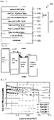
- Figure 1 illustrates a schematic sectional view of an organic electroluminescent device comprising the electron buffering material according to one embodiment of the present invention.
- injection and transport of electrons can be controlled due to the difference of affinities between the light-emitting layer and the electron transport zone in accordance with LUMO energy levels.
- Figure 2 illustrates an energy gap relationship among the layers of the organic electroluminescent device according to one embodiment of the present invention.
- FIG. 3 A comparison between when an electron buffer layer is comprised and when an electron buffer layer is not comprised is illustrated in Figure 3 .
- An organic electroluminescent device in which an electron buffer layer is inserted has higher current efficiency. The above will be described in detail hereinafter.
- a nitrogen-containing heteroaryl is a triazine derivative, a pyrimidine derivative, a quinazoline derivative, a quinoxaline derivative. Electron injection characteristics can be controlled by varying the nitrogen-containing heteroaryl.
- An electron buffering material compound comprising a triazine derivative can obtain suitable efficiency and lifespan characteristic through a specific level of restraint of electron injection by taking advantage of an appropriate barrier against the light-emitting layer.
- An electron buffering material compound comprising a pyrimidine derivative can contribute to efficiency increase of the device by minimizing the electron injection barrier from the light-emitting layer in accordance with low LUMO energy levels.
- An electron buffering material compound comprising a quinazoline or quinoxaline shows a big improvement of lifespan rather than the efficiency of the device by excessive electron injection block in accordance with high LUMO energy levels.
- the compound comprising a nitrogen-containing heteroaryl, being triazine, pyrimidine, quinazoline or quinoxaline, and comprised in the electron buffering material is selected from the compounds represented by the following formulae 1 to 3: H-(Cz-L 1 ) a -M (1) H-(Cz) b -L 1 -M (2) wherein
- the specific compounds of which the nitrogen-containing heteroaryl is triazine include the following compounds, but are not limited thereto:
- the specific compounds of which the nitrogen-containing heteroaryl is pyrimidine include the following compounds, but are not limited thereto:
- the specific compounds of which the nitrogen-containing heteroaryl is quinoline include the following compounds, but are not limited thereto:
- the specific compounds of which the nitrogen-containing heteroaryl is quinoxaline include the following compounds, but are not limited thereto:
- the thickness of the electron buffer layer (126) can be 1 nm or more, but is not limited specifically. In detail, the thickness of the electron buffer layer (126) can be from 2 to 100 nm.
- the electron buffer layer (126) can be formed on the light-emitting layer (125) in various methods that are known such as vacuum evaporation method, wet film-forming method, laser transfer method, etc.
- the light-emitting layer comprised in the organic electroluminescent device of the present invention can comprise a host and a dopant.
- the host compound can be a phosphorescent host compound or a fluorescent host compound.
- the dopant compound can be a phosphorescent dopant compound or a fluorescent dopant compound.
- the host compound and the dopant compound can be a fluorescent host compound and a fluorescent dopant compound, respectively.
- Anthracene derivatives aluminum complexes, rubrene derivatives, arylamine derivatives, etc., can be used as a host material, and preferably, anthracene derivatives.
- Examples of the host materials of the present invention include the following compounds, but are not limited thereto:
- Examples of the dopant materials of the present invention include the following compounds, but are not limited thereto:
- the dopant can be doped in an amount of less than about 25 wt%, preferably less than about 17 wt%, based on the total amount of the dopant and host of the light-emitting layer.
- the thickness of the light-emitting layer (125) can be from about 5 nm to 100 nm, preferably from about 10 nm to 60 nm.
- Light emission occurs at the light-emitting layer, and the light-emitting layer can be a mono- or multi-layer.
- each light-emitting layer can emit different colors of light.
- a white light-emitting device can be produced by forming three light-emitting layers (125) that emit blue, red, and green, respectively.
- the light-emitting layer (125) can be formed on the hole transport layer (123) in various methods that are known such as vacuum evaporation method, wet film-forming method, laser transfer method, etc.
- the organic electroluminescent device of the present invention may additionally comprises a hole injection layer or a hole transport layer between the first electrode and the light-emitting layer.
- the organic electroluminescent device (100) comprises a substrate (101), a first electrode (110) formed on the substrate (101), an organic layer (120) formed on the first electrode (110), and a second electrode (130) facing the first electrode (110) formed on the organic layer (120).
- the organic layer (120) comprises a hole injection layer (122), a hole transport layer (123) formed on the hole injection layer (122), a light-emitting layer (125) formed on the hole transport layer (123), an electron buffer layer (126) formed on the light-emitting layer (125), and an electron transport zone (129) formed on the electron buffer layer (126).
- the electron transport zone (129) comprises an electron transport layer (127) formed on the electron buffer layer (126), and an electron injection layer (128) formed on the electron transport layer (127).
- the substrate (101) can be a glass substrate, a plastic substrate, or a metal substrate used in a general organic electroluminescent device.
- the first electrode (110) can be an anode, and can be formed by a material which has high work function.
- Materials for the first electrode (110) can be indium tin oxide (ITO), tin oxide (TO), indium zinc oxide (IZO), indium tin zinc oxide (ITZO), or a mixture thereof.
- the first electrode (110) can be formed in various methods that are known such as evaporation method, sputtering method, etc.
- phthalocyanine compounds such as copper phthalocyanine, MTDATA (4,4',4"-tris[(3-methylphenyl)phenylamino]triphenylamine), 2-TNATA (4,4',4"-tris[2-naphthyl(phenyl)amino]triphenylamine), N 1 ,N 1' -([1,1'-biphenyl]-4,4'-diyl)bis(N 1 -(naphthalen-1-yl)-N 4 ,N 4 -diphenylbenzene-1,4-diamine), Pani/DBSA (polyaniline/dodecylbenzenesulfonic acid), PEDOT/PSS (poly(3,4-ethylenedioxythiophene)/poly(4-styrenesulfonate)), Pani/CSA (polyaniline/camphorsulfonic acid
- the hole injection layer (122) can be formed by using the following compound of formula 11: wherein R is selected from a group consisting of a cyano (-CN), a nitro (-NO 2 ), phenylsulfonyl (-SO 2 (C 6 H 5 )), a (C2-C5)alkenyl substituted with cyano or nitro, and a phenyl substituted with cyano or nitro.
- the compound of formula 11 has a characteristic of being crystallized. Accordingly, the hole injection layer (122) can obtain strength by using the compound.
- the hole injection layer (122) can be a mono- or multi-layer. When the hole injection layer (122) is a multi-layer of two or more layers, the compound of formula 11 can be used in one of them.
- the thickness of the hole injection layer (122) can be from about 1 nm to about 1,000 nm, preferably from about 5 nm to 100 nm.
- the hole injection layer (122) can be formed on the first electrode (110) in various methods that are known such as vacuum evaporation method, wet film-forming method, laser transfer method, etc.
- Examples of the hole injection material comprised in the hole injection layer include the following compounds, but are not limited thereto:
- Materials used in the hole transport layer (123) can be known hole transport materials.
- aromatic amine-based derivatives specifically biphenyl diamine-based derivatives such as TPD(N,N'-bis-(3-methylphenyl)-N,N'-diphenylbenzydine), N 4 ,N 4 ,N 4' ,N 4' -tetra([1,1'-biphenyl]-4-yl-[1,1'-biphenyl]-4,4'-diamine can be used, but are not limited thereto.
- Examples of the hole transport material comprised in the hole transport layer include the following compounds, but are not limited thereto:
- the hole transport layer (123) can be a mono- or multi-layer.
- the thickness of the hole transport layer (123) can be from about 1 nm to about 100 nm, preferably from about 5 nm to 80 nm.
- the hole transport layer (123) can be formed on the hole injection layer (122) in various methods that are known such as vacuum evaporation method, wet film-forming method, laser transfer method, etc.
- the lifespan of the device becomes longer due to stabilized hole transport layer even for organic electroluminescent devices comprising an electron buffer layer of which lifespan is relatively short, i.e. upon comparing using a material of which HOMO characteristics and anion stability are improved to using a material of which HOMO characteristics and anion stability are vulnerable for a hole transport material of the hole transport layer, lifespan characteristics can be prevented from being decreased by using a material of which HOMO characteristics and anion stability are improved, due to relatively low deviation of lifespan according to the material groups consisting of the electron buffer layer even for a device comprising an electron buffer layer of which lifespan is relatively short.
- Materials used in the electron transport layer (127) can be known electron transport materials.
- electron transport materials For example, oxazole-based compounds, isoxazole-based compounds, triazole-based compounds, isothiazole-based compounds, oxadiazole-based compounds, thiadiazole-based compounds, perylene-based compounds, anthracene-based compounds, aluminum complexes, gallium complexes, etc., can be used, but are not limited thereto.
- Examples of the electron transport material comprised in the electron transport layer include the following compounds, but are not limited thereto:
- the electron transport layer (127) can be a mixed layer comprising an electron transport compound and a reductive dopant.
- the electron transport compound When formed as a mixed layer, the electron transport compound reduces to an anion so that electrons can be easily injected and transported to a light-emitting medium.
- the electron transport compound is not specifically limited, and the known electron transport material can be used.
- the reductive dopant can be alkali metals, alkali metal compounds, alkaline-earth metals, rare earth metals, halides thereof, oxides thereof, and complexes thereof.
- Specific examples of the reductive dopant include lithium quinolate, sodium quinolate, cesium quinolate, potassium quinolate, LiF, NaCl, CsF, Li 2 O, BaO, and BaF 2 , but are not limited thereto.
- the thickness of the electron transport layer (127) can be from about 5 nm to about 100 nm, preferably from about 10 nm to about 60 nm.
- the electron transport layer (127) can be formed on the electron buffer layer (126) in various methods that are known such as vacuum evaporation method, wet film-forming method, laser transfer method, etc.
- Materials used in the electron injection layer (128) can be known electron injection materials.
- lithium quinolate, sodium quinolate, cesium quinolate, potassium quinolate, LiF, NaCl, CsF, Li 2 O, BaO, BaF 2 , etc. can be used, but are not limited thereto.
- the thickness of the electron injection layer (128) can be from about 0.1 to about 10 nm, and preferably from about 0.3 nm to about 9 nm.
- the electron injection layer (128) can be formed on the electron transport layer (127) in various methods that are known such as vacuum evaporation method, wet film-forming method, laser transfer method, etc.
- Lithium quinoline complex metal can be used as the electron injection material comprised in the electron injection layer. Specifically, it can be exemplified as the following compound, but is not limited thereto.
- the second electrode (130) can be a cathode, and can be formed by a material which has low work function.
- Materials for the second electrode (130) can be aluminum (Al), calcium (Ca), magnesium (Mg), silver (Ag), cesium (Cs), lithium (Li), or a combination thereof.
- the second electrode (130) can be formed in various methods that are known such as evaporation method, sputtering method, etc.
- the organic electroluminescent device of Figure 1 is only an embodiment to be explained clearly, and the present invention should not be limited to the embodiment but can be varied to another mode.
- an optional component of the organic electroluminescent device of Figure 1 besides a light-emitting layer and an electron buffer layer can be omitted such as the hole injection layer.
- an optional component can be further added. Examples of the further added optional component are impurity layers such as n-doping layer and p-doping layer.
- the organic electroluminescent device can emit light from both sides by placing a light-emitting layer each in both sides in between the impurity layers. The light-emitting layers of both sides can emit different colors.
- the first electrode can be a transparent electrode and the second electrode can be a reflective electrode so that the organic electroluminescent device can be a bottom emission type
- the first electrode can be a reflective electrode and the second electrode can be a transparent electrode so that the organic electroluminescent device can be a top emission type
- a cathode, an electron transport layer, a light-emitting layer, a hole transport layer, a hole injection layer, and an anode can be sequentially stacked on a substrate to be an inverted organic electroluminescent device.
- Figure 2 illustrates an energy gap relationship among the layers of the organic electroluminescent device according to one embodiment of the present invention.
- a hole transport layer (123), a light-emitting layer (125), an electron buffer layer (126), and an electron transport zone (129) are sequentially stacked, and electrons are injected from the cathode to the light-emitting layer (125) through the electron transport zone (129) and the electron buffer layer (126).
- the LUMO energy level of the electron buffer layer (126) is higher than that of the host compound and the dopant compound of the light-emitting layer (125), and that of the electron transport layer (127). Specifically, LUMO energy levels have the following equational relationship: electron buffer layer > electron transport zone > host compound. According to conventional techniques, the light-emitting area of the light-emitting layer (125) has been shifted to the hole transport layer (123) side due to hole trap and emitted light at the interface.
- the electron buffer layer (126) has a LUMO energy level as described above to allow an electron trap to occur so that the light-emitting area of the light-emitting layer shifts to the electron transport zone (129) side, thus the lifespan and efficiency of the organic electroluminescent device can be improved.
- the HOMO energy level of the electron buffer layer (126) is higher than that of the dopant compound of the light-emitting layer (125), but is lower than that of the host compound and the electron transport zone (129).
- the LUMO energy levels of the present invention can be easily measured by known various methods. Generally, LUMO energy levels are measured by cyclic voltammetry or ultraviolet photoelectron spectroscopy (UPS). Therefore, a person skilled in the art can easily comprehend the electron buffer layer, host material, and electron transport zone that satisfy the equational relationship of the LUMO energy levels of the present invention, and practice the present invention. HOMO energy levels can be easily measured by the same method of measuring LUMO energy levels.
- the LUMO energy level of the host (Ah) is higher than that of the dopant (Ad).
- the LUMO energy level of the electron buffer layer (Ab) is higher than that of the host (Ah).
- the LUMO energy level of the electron buffer layer and the LUMO energy level of the host (Ah) have the following equational relationship: Ab ⁇ Ah + 0.5 eV
- the LUMO energy level of the electron buffer layer (Ab) can be set to have the following equational relationship: Ab ⁇ Ah + 0.2 ⁇ 0.3 eV
- the LUMO energy level of the electron buffer layer (Ab) can be set to have the following equational relationship: Ab ⁇ Ah + 0.3 ⁇ 0.5 eV
- the LUMO energy level of the electron buffer layer (Ab) can be set to have the following equational relationship: Ab ⁇ Ah + 0.3 eV
- the electron buffer layer can be comprised in organic electroluminescent devices emitting every color including blue, red, and green. Preferably, it can be comprised in an organic electroluminescent device emitting blue light (i.e. the main peak wavelength is from 430 to 470 nm, preferably, in the 450's nm).
- Examples 1 to 3 Organic electroluminescent device comprising an electron buffering material comprising a triazine derivative
- An OLED device of the present invention was produced.
- a transparent electrode indium tin oxide (ITO) thin film (15 ⁇ /sq) on a glass substrate for an organic light-emitting diode (OLED) device (Samsung-Corning) was subjected to an ultrasonic washing with acetone, ethanol, and distilled water, sequentially, and then was stored in isopropanol.
- the ITO substrate was then mounted on a substrate holder of a vacuum vapor depositing apparatus.
- N 4 ,N 4' -diphenyl-N 4 ,N 4' -bis(9-phenyl-9H-carbazol-3-yl)-[1,1'-biphenyl]-4,4'-diamine was introduced into a cell of said vacuum vapor depositing apparatus, and then the pressure in the chamber of said apparatus was controlled to 10 -6 torr. Thereafter, an electric current was applied to the cell to evaporate the above introduced material, thereby forming a hole injection layer having a thickness of 40 nm on the ITO substrate.
- 1,4,5,8,9,11-hexaazatriphenylene-hexacarbonitrile was then introduced into another cell of said vacuum vapor depositing apparatus, and was evaporated by applying an electric current to the cell, thereby forming a hole injection layer having a thickness of 5 nm on the hole injection layer.
- N-([1,1'-biphenyl]-4-yl)-9,9-dimethyl-N-(4-(9-phenyl-9H-carbazol-3-yl)phenyl)-9H-fluorene-2-amine was introduced into another cell of said vacuum vapor depositing apparatus, and was evaporated by applying an electric current to the cell, thereby forming a hole transport layer having a thickness of 25 nm on the hole injection layer.
- compound H-1 was introduced into one cell of the vacuum vapor depositing apparatus, as a host material, and compound D-2 was introduced into another cell as a dopant.
- the two materials were evaporated at different rates and were deposited in a doping amount of 2 wt% based on the total amount of the host and dopant to form a light-emitting layer having a thickness of 20 nm on the hole transport layer.
- 2-(4-(9,10-di(naphthalen-2-yl)anthracen-2-yl)phenyl)-1-phenyl-1H-benzo[d]imidazole was then introduced into one cell and lithium quinolate was introduced into another cell.
- the two materials were evaporated at the same rate and deposited in a doping amount of 50 wt% each to form an electron transport layer having a thickness of 27 nm on the light-emitting layer. Thereafter, an electron buffer layer having a thickness of 9 nm was inserted between the light-emitting layer and the electron transport layer. After depositing lithium quinolate as an electron injection layer having a thickness of 2 nm on the electron transport layer, an Al cathode having a thickness of 80 nm was then deposited by another vacuum vapor deposition apparatus on the electron injection layer. Thus, an OLED device was produced. All the materials used for producing the OLED device were purified by vacuum sublimation at 10 -6 torr prior to use. The driving voltage based on a luminance of 1,000 nits, luminous efficiency, CIE color coordinate, and lifespan of 10 hours based on a luminance of 2,000 nits and constant-current were measured.
- Comparative Example 1 Organic electroluminescent device not comprising an electron buffering material
- An OLED device was produced in the same manner as in Examples 1 to 3, except for increasing the thickness of the electron transport layer to 36 nm instead of forming the electron transport layer of 27 nm and the electron buffer layer of 9 nm.
- the LUMO energy levels of the electron buffer layer are in the mid-1.9's eV or higher so that the electron injection barrier at the interface between the light-emitting layer and the electron buffer layer is minimized to show fast electron injection characteristics, while showing similar voltage characteristics compared to Comparative Example 1.
- the LUMO energy levels of Examples 1 and 2 maintain 1.8's eV and obtained appropriate electron injection characteristics to show high efficiency.
- the lifespans of Examples 1 to 3 were similar to Comparative Example 1.
- Examples 4 to 7 Organic electroluminescent device comprising an electron buffering material comprising a triazine derivative
- An OLED device was produced in the same manner as in Examples 1 to 3, except for using different electron buffering materials.
- the LUMO energy levels of the electron buffer layer are between the mid- and high 1.9's eV and 2.0 eV so that the electron injection barrier of the interface between the light-emitting layer and the electron buffer layer affects much, and thus showed slow electron injection characteristics compared to Comparative Example 1.
- higher voltage characteristics were shown compared to Comparative Example 1. Accordingly, the injected electrons are not relatively sufficient compared to holes, and the possibility of forming excitons is dropped to show lower efficiency compared to Comparative Example 1. However, longer lifespans were shown compared to Comparative Example 1.
- Examples 8 to 12 Organic electroluminescent device comprising an electron buffering material comprising a triazine derivative
- An OLED device was produced in the same manner as in Examples 1 to 3, except for using different electron buffering materials.
- the LUMO energy levels of the electron buffer layer are formed at the mid-1.9's eV, and a specific level of electron injection barrier is applied so that appropriate electron injection characteristics are shown which satisfy both efficiency and lifespan.
- higher efficiency and longer lifespan were shown compared to Comparative Example 1.
- excellent lifespan characteristics were shown, i.e. 1.5% or more compared to Comparative Example 1 while showing high efficiency.
- Examples 13 to 15 Organic electroluminescent device comprising an electron buffering material comprising a pyrimidine derivative
- An OLED device was produced in the same manner as in Examples 1 to 3, except for using different electron buffering materials.
- the LUMO energy levels of the electron buffer layer are formed in the mid-1.7's to 1.8's eV, and the electron injection barrier of the interface between the light-emitting layer and the electron buffer layer decreased compared to triazine derivatives to produce an organic electroluminescent device having fast voltage characteristics and fairly improved efficiency.
- lifespan was similar or worse compared to Comparative Example 1 and worse than triazine derivatives.
- Examples 16 to 18 Organic electroluminescent device comprising an electron buffering material comprising a quinazoline or quinoxaline derivative
- An OLED device was produced in the same manner as in Examples 1 to 3, except for using different electron buffering materials.
- the LUMO energy levels of the electron buffer layer are maintained in the mid-1.9's to 2.0's eV. Although the LUMO energy levels of some of the electron buffer layers were maintained in the mid-1.9's, the electron injection ability of the quinazoline and quinoxaline derivatives were dropped drastically compared to triazine or pyrimidine derivatives so that a device having slow voltage characteristics and decreased efficiency was produced. On the contrary, higher lifespan characteristics were shown compared to Comparative Example 1. This is due to interfacial light emission between the electron transport layer and the light-emitting layer being mitigated as a result of the decline of electron injection ability caused by the electron buffer layer.
- An OLED device was produced in the same manner as in Examples 1 to 3, except for using different electron buffering materials.
- Examples 19 and 20 characteristics of the device were compared according to existence of phenyl between the carbazole derivative and the triazine derivative.
- the electron injection was disrupted due to increase of the LUMO energy values of Example 19 compared to Example 20 by inserting a phenyl therebetween.
- high driving voltage and low efficiency were shown, but the lifespan improved.
- Examples 21 and 22 characteristics of the device were compared according to existence of phenyl between the carbazole derivative and the triazine derivative.
- the electron injection was disrupted due to increase of the LUMO energy values of Example 21 compared to Example 22 by inserting a phenyl therebetween.
- high driving voltage and low efficiency were shown, but the lifespan improved.
- similar tendency was shown regardless of meta or para substitution position of phenyl.
- higher LUMO energy level difference was shown in Example 22 in which substitution was made at the meta position.
- An OLED device was produced in the same manner as in Examples 1 to 3, except for using different electron buffering materials.
- triazine and quinazoline derivatives determining the LUMO energy level were compared by identically maintaining the derivative of the HOMO orbital zone for checking the device characteristics according to the derivatives determining the LUMO energy level.
- Example 24 of a triazine derivative the LUMO energy level increased in that the electron injection was highly disrupted in Example 23 of a quinazoline derivative, and thus showed improved lifespan in spite of high driving voltage and low efficiency.
- Example 26 of a quinoxaline derivative In contrast to Example 25 of a triazine derivative, the LUMO energy level increased in that the electron injection was highly disrupted in Example 26 of a quinoxaline derivative, and thus showed improved lifespan in spite of high driving voltage and low efficiency.
- quinazoline and quinoxaline derivatives showed higher x- and y-coordinates compared to triazine derivatives. This is due to the electron injection ability being dropped due to the electron buffer layer, and the HOMO energy level of the electron buffer layer being lower than that of the anthracene host while the light-emitting zone got further from the interface between the electron transport layer and the light-emitting layer so that the excitons were not bounded within the light-emitting layer, and the electron buffer layer contributed to light emission.
- Example 27 an OLED device comprising an electron buffer layer was produced having the same constitution as in Example 22, except for varying the electron transport layer.
- Comparative Example 6 and Examples 32 to 35 Organic electroluminescent device comprising a multi-layered hole transport layer and comprising or non-comprising an electron buffer layer
- Comparative Example 6 an OLED device was produced in the same manner as in Comparative Example 1, except for inserting two separate hole transport layers of 20 nm and 5 nm, respectively, rather than one hole transport layer of 25 nm, and changing the thickness of HI-1 to 60 nm.
- Examples 32 to 35 an OLED device comprising an electron buffer layer was produced having the same constitution as in Comparative Example 6, except for varying the electron buffer layer.
- Comparative Example 7 and Examples 36 to 39 Organic electroluminescent device comprising a multi-layered hole transport layer and comprising or non-comprising an electron buffer layer
- Comparative Example 7 an OLED device was produced in the same manner as in Comparative Example 6, except for changing hole transport layer 2 to another derivative.
- an OLED device comprising an electron buffer layer was produced having the same constitution as in Example 32, except for changing the hole transport layer and the electron buffer layer.
- Comparative Examples 8 to 11 and Examples 40 to 43 Organic electroluminescent device comprising various light-emitting materials and comprising or non-comprising an electron buffer layer
- Comparative Examples 8 to 10 an OLED device was produced in the same manner as in Comparative Example 1, except for varying the host to another derivative.
- Examples 40 to 42 an OLED device was produced in the same manner as in Comparative Example 8, except for shortening the thickness of the electron transport layer to 27 nm, and inserting an electron buffer layer of 9 nm between the light-emitting layer and the electron transport layer.
- Comparative Example 11 an OLED device was produced in the same manner as in Comparative Example 1, except for changing the blue dopant to compound D-1.
- Example 43 an OLED device was produced in the same manner as in Comparative Example 11, except for shortening the thickness of the electron transport layer to 27 nm, and inserting an electron buffer layer of 9 nm between the light-emitting layer and the electron transport layer.
- Examples 40 to 42 hosts other than H-1 were used since C-1 material was used for the electron buffer layer which can improve lifespan compared to Comparative Examples 8 to 10. As a result, similar tendency was shown compared to a device not having any electron buffer layer even for other hosts.
Landscapes
- Chemical & Material Sciences (AREA)
- Organic Chemistry (AREA)
- Engineering & Computer Science (AREA)
- Materials Engineering (AREA)
- Physics & Mathematics (AREA)
- Spectroscopy & Molecular Physics (AREA)
- Inorganic Chemistry (AREA)
- Optics & Photonics (AREA)
- Electroluminescent Light Sources (AREA)
- Nitrogen Condensed Heterocyclic Rings (AREA)
- Plural Heterocyclic Compounds (AREA)
- Heterocyclic Carbon Compounds Containing A Hetero Ring Having Oxygen Or Sulfur (AREA)
Applications Claiming Priority (3)
| Application Number | Priority Date | Filing Date | Title |
|---|---|---|---|
| KR20140031264 | 2014-03-17 | ||
| KR1020150036184A KR20150108330A (ko) | 2014-03-17 | 2015-03-16 | 전자 버퍼 재료 및 이를 포함하는 유기 전계 발광 소자 |
| PCT/KR2015/002580 WO2015142036A1 (en) | 2014-03-17 | 2015-03-17 | Electron buffering material and organic electroluminescent device comprising the same |
Publications (4)
| Publication Number | Publication Date |
|---|---|
| EP3119767A1 EP3119767A1 (en) | 2017-01-25 |
| EP3119767A4 EP3119767A4 (en) | 2017-11-08 |
| EP3119767B1 EP3119767B1 (en) | 2019-07-10 |
| EP3119767B2 true EP3119767B2 (en) | 2022-06-29 |
Family
ID=54246382
Family Applications (1)
| Application Number | Title | Priority Date | Filing Date |
|---|---|---|---|
| EP15764173.9A Active EP3119767B2 (en) | 2014-03-17 | 2015-03-17 | Organic electroluminescent device comprising electron buffering material |
Country Status (6)
| Country | Link |
|---|---|
| US (2) | US20170117485A1 (zh) |
| EP (1) | EP3119767B2 (zh) |
| JP (1) | JP2017510071A (zh) |
| KR (1) | KR20150108330A (zh) |
| CN (1) | CN106068267B (zh) |
| TW (1) | TW201600519A (zh) |
Families Citing this family (35)
| Publication number | Priority date | Publication date | Assignee | Title |
|---|---|---|---|---|
| WO2015090504A2 (de) * | 2013-12-19 | 2015-06-25 | Merck Patent Gmbh | Heterocyclische spiroverbindungen |
| KR101537499B1 (ko) * | 2014-04-04 | 2015-07-16 | 주식회사 엘지화학 | 유기 발광 소자 |
| KR102457008B1 (ko) * | 2014-05-23 | 2022-10-19 | 가부시키가이샤 한도오따이 에네루기 켄큐쇼 | 헤테로고리 화합물, 발광 소자, 발광 장치, 전자 기기, 및 조명 장치 |
| EP3174887A4 (en) * | 2014-07-29 | 2018-04-04 | Rohm And Haas Electronic Materials Korea Ltd. | Electron buffering material and organic electroluminescent device |
| KR102369595B1 (ko) * | 2014-12-08 | 2022-03-04 | 삼성디스플레이 주식회사 | 유기 발광 소자 및 이를 포함하는 표시 장치 |
| EP3269789B1 (en) | 2015-03-09 | 2023-08-30 | Hodogaya Chemical Co., Ltd. | Light emitting material and organic electroluminescent element |
| JP2018517289A (ja) * | 2015-05-29 | 2018-06-28 | ダウ グローバル テクノロジーズ エルエルシー | 有機組成物及び該組成物を含む有機層を備える電子デバイス |
| KR20170010715A (ko) | 2015-07-20 | 2017-02-01 | 롬엔드하스전자재료코리아유한회사 | 지연 형광용 발광 재료 및 이를 포함하는 유기 전계 발광 소자 |
| KR102494453B1 (ko) * | 2015-10-05 | 2023-02-02 | 삼성디스플레이 주식회사 | 유기 전계 발광 소자 및 이를 포함하는 표시 장치 |
| JP6788314B2 (ja) * | 2016-01-06 | 2020-11-25 | コニカミノルタ株式会社 | 有機エレクトロルミネッセンス素子、有機エレクトロルミネッセンス素子の製造方法、表示装置及び照明装置 |
| KR102549533B1 (ko) * | 2016-02-25 | 2023-06-30 | 삼성디스플레이 주식회사 | 유기 전계 발광 소자 |
| CN114805337A (zh) * | 2016-03-15 | 2022-07-29 | 陶氏环球技术有限责任公司 | 有机电致发光化合物和其有机电致发光器件 |
| KR102547468B1 (ko) | 2016-09-13 | 2023-06-27 | 롬엔드하스전자재료코리아유한회사 | 전자 버퍼층 및 전자 전달층을 포함하는 유기 전계 발광 소자 |
| KR102455656B1 (ko) | 2016-09-22 | 2022-10-19 | 롬엔드하스전자재료코리아유한회사 | 전자 버퍼층 및 전자 전달층을 포함하는 유기 전계 발광 소자 |
| KR20180035554A (ko) | 2016-09-29 | 2018-04-06 | 롬엔드하스전자재료코리아유한회사 | 전자 전달층 및 전자 버퍼층을 포함하는 유기 전계 발광 소자 |
| KR102582797B1 (ko) * | 2017-01-10 | 2023-09-27 | 롬엔드하스전자재료코리아유한회사 | 유기 전계 발광 소자 |
| KR102613183B1 (ko) * | 2017-02-28 | 2023-12-14 | 롬엔드하스전자재료코리아유한회사 | 유기 전계 발광 소자 |
| JP6740560B2 (ja) * | 2017-03-09 | 2020-08-19 | エルジー・ケム・リミテッド | 有機発光素子 |
| CN109890812B (zh) * | 2017-03-27 | 2021-11-23 | 株式会社Lg化学 | 杂环化合物和包含其的有机发光器件 |
| KR102171941B1 (ko) * | 2017-09-22 | 2020-10-30 | 주식회사 엘지화학 | 신규한 화합물 및 이를 포함하는 유기 발광 소자 |
| KR20190036458A (ko) * | 2017-09-26 | 2019-04-04 | 삼성디스플레이 주식회사 | 유기 발광 소자 |
| KR102160270B1 (ko) * | 2017-10-20 | 2020-09-25 | 삼성에스디아이 주식회사 | 유기 광전자 소자용 조성물, 유기 광전자 소자 및 표시 장치 |
| US10249832B1 (en) | 2017-12-06 | 2019-04-02 | Idemitsu Kosan Co., Ltd. | Organic electroluminescence device and novel compound |
| KR20190070586A (ko) | 2017-12-13 | 2019-06-21 | 엘지디스플레이 주식회사 | 전자수송 재료용 화합물 및 이를 포함하는 유기 발광 다이오드 |
| EP3503240A1 (en) * | 2017-12-21 | 2019-06-26 | Novaled GmbH | Organic semiconductor layer |
| EP3880672A1 (de) * | 2018-11-16 | 2021-09-22 | cynora GmbH | Carbazolderivate zur verwendung in optoelektronischen vorrichtungen |
| CN116621842A (zh) * | 2019-01-25 | 2023-08-22 | 株式会社Lg化学 | 化合物及包含其的有机发光器件 |
| WO2020153652A1 (ko) * | 2019-01-25 | 2020-07-30 | 주식회사 엘지화학 | 화합물 및 이를 포함하는 유기발광소자 |
| US20220029107A1 (en) * | 2019-02-28 | 2022-01-27 | Lg Chem, Ltd. | Compound and organic light emitting device comprising same |
| KR102654051B1 (ko) * | 2019-09-11 | 2024-04-03 | 주식회사 엘지화학 | 화합물 및 이를 포함하는 유기 발광 소자 |
| KR102222845B1 (ko) * | 2020-05-18 | 2021-03-03 | 엘지디스플레이 주식회사 | 전자수송 재료용 화합물 및 이를 포함하는 유기 발광 다이오드 |
| KR20220033737A (ko) * | 2020-09-10 | 2022-03-17 | 엘지디스플레이 주식회사 | 유기 화합물, 이를 포함하는 유기발광다이오드 및 유기발광장치 |
| CN112993199B (zh) * | 2021-02-25 | 2023-03-07 | 上海弗屈尔光电科技有限公司 | 一种三元组合物及含有该组合物的有机发光元件与应用 |
| KR20230170185A (ko) * | 2022-06-09 | 2023-12-19 | 삼성디스플레이 주식회사 | 발광 소자 및 이를 포함하는 표시 장치 |
| CN115181095B (zh) * | 2022-07-06 | 2024-03-22 | 天津大学 | 具有荧光-延迟荧光-室温磷光三重发射特性的嘧啶基发光体及其制备方法 |
Citations (3)
| Publication number | Priority date | Publication date | Assignee | Title |
|---|---|---|---|---|
| US20060029828A1 (en) † | 2004-03-25 | 2006-02-09 | Hiroshi Kanno | Organic electroluminescent device |
| US20110037062A1 (en) † | 2008-03-17 | 2011-02-17 | Nippon Steel Chemical Co., Ltd. | Organic electroluminescent device |
| JP2013197323A (ja) † | 2012-03-21 | 2013-09-30 | Konica Minolta Inc | 有機エレクトロルミネッセンス素子 |
Family Cites Families (50)
| Publication number | Priority date | Publication date | Assignee | Title |
|---|---|---|---|---|
| JP4848134B2 (ja) * | 2005-04-18 | 2011-12-28 | 出光興産株式会社 | 芳香族アミン誘導体及びそれを用いた有機エレクトロルミネッセンス素子 |
| US9666826B2 (en) * | 2005-11-30 | 2017-05-30 | Global Oled Technology Llc | Electroluminescent device including an anthracene derivative |
| WO2010022101A2 (en) * | 2008-08-19 | 2010-02-25 | Plextronics, Inc. | Organic light emitting diode lighting devices |
| DE102009012346B4 (de) * | 2009-03-09 | 2024-02-15 | Merck Patent Gmbh | Organische Elektrolumineszenzvorrichtung und Verfahren zu deren Herstellung |
| KR101477613B1 (ko) * | 2009-03-31 | 2014-12-30 | 롬엔드하스전자재료코리아유한회사 | 신규한 유기 전자재료용 화합물 및 이를 포함하는 유기 전자 소자 |
| DE102009031021A1 (de) * | 2009-06-30 | 2011-01-05 | Merck Patent Gmbh | Materialien für organische Elektrolumineszenzvorrichtungen |
| KR20110013220A (ko) * | 2009-07-31 | 2011-02-09 | 다우어드밴스드디스플레이머티리얼 유한회사 | 신규한 유기 발광 화합물 및 이를 포함하는 유기 전계 발광 소자 |
| WO2011014039A1 (en) * | 2009-07-31 | 2011-02-03 | Rohm And Haas Electronic Materials Korea Ltd. | Novel organic electroluminescent compounds and organic electroluminescent device using the same |
| KR101431644B1 (ko) * | 2009-08-10 | 2014-08-21 | 롬엔드하스전자재료코리아유한회사 | 신규한 유기 발광 화합물 및 이를 포함하는 유기 전계 발광 소자 |
| DE102009041289A1 (de) * | 2009-09-16 | 2011-03-17 | Merck Patent Gmbh | Organische Elektrolumineszenzvorrichtung |
| KR101506999B1 (ko) * | 2009-11-03 | 2015-03-31 | 제일모직 주식회사 | 유기광전소자용 화합물 및 이를 포함하는 유기광전소자 |
| DE102009052428A1 (de) * | 2009-11-10 | 2011-05-12 | Merck Patent Gmbh | Verbindung für elektronische Vorrichtungen |
| KR20110094271A (ko) * | 2009-12-16 | 2011-08-23 | 이데미쓰 고산 가부시키가이샤 | 유기 발광 매체 |
| KR20110122051A (ko) * | 2010-05-03 | 2011-11-09 | 제일모직주식회사 | 유기광전소자용 화합물 및 이를 포함하는 유기광전소자 |
| JPWO2011148909A1 (ja) * | 2010-05-24 | 2013-07-25 | 出光興産株式会社 | 有機エレクトロルミネッセンス素子 |
| KR101420318B1 (ko) * | 2010-06-17 | 2014-07-16 | 이-레이 옵토일렉트로닉스 테크놀로지 컴퍼니 리미티드 | 유기전계발광장치용 화합물 및 이를 포함하는 유기전계발광장치 |
| JP5821635B2 (ja) * | 2010-06-24 | 2015-11-24 | 東レ株式会社 | 発光素子材料および発光素子 |
| KR20120030941A (ko) * | 2010-09-20 | 2012-03-29 | 롬엔드하스전자재료코리아유한회사 | 신규한 유기 발광 화합물 및 이를 채용하고 있는 유기 전계 발광 소자 |
| WO2012039561A1 (en) * | 2010-09-20 | 2012-03-29 | Rohm And Haas Electronic Materials Korea Ltd. | Novel organic electroluminescent compounds and organic electroluminescent device using the same |
| KR20120038060A (ko) * | 2010-10-13 | 2012-04-23 | 롬엔드하스전자재료코리아유한회사 | 신규한 유기 전자재료용 화합물 및 이를 포함하는 유기 전계 발광 소자 |
| KR101531904B1 (ko) * | 2010-10-13 | 2015-06-29 | 롬엔드하스전자재료코리아유한회사 | 신규한 유기 전자재료용 화합물 및 이를 포함하는 유기 전계 발광 소자 |
| JP5673043B2 (ja) * | 2010-12-03 | 2015-02-18 | 東洋インキScホールディングス株式会社 | 有機エレクトロルミネッセンス素子 |
| WO2012099241A1 (ja) * | 2011-01-20 | 2012-07-26 | 出光興産株式会社 | 有機エレクトロルミネッセンス素子 |
| KR101427611B1 (ko) * | 2011-03-08 | 2014-08-11 | 롬엔드하스전자재료코리아유한회사 | 신규한 유기 전자재료용 화합물 및 이를 포함하는 유기 전계 발광 소자 |
| KR20120109744A (ko) * | 2011-03-25 | 2012-10-09 | 롬엔드하스전자재료코리아유한회사 | 신규한 유기 전자재료용 화합물 및 이를 포함하는 유기 전계 발광 소자 |
| JP6197265B2 (ja) * | 2011-03-28 | 2017-09-20 | 東レ株式会社 | 発光素子材料および発光素子 |
| KR20120116269A (ko) * | 2011-04-12 | 2012-10-22 | 롬엔드하스전자재료코리아유한회사 | 신규한 유기 전자재료용 화합물 및 이를 포함하는 유기 전계 발광 소자 |
| EP2694619A4 (en) * | 2011-05-03 | 2014-10-22 | Rohm & Haas Elect Mat | NOVEL ORGANIC ELECTROLUMINESCENT COMPOUNDS AND ORGANIC ELECTROLUMINESCENT DEVICE USING THE SAME |
| KR101799077B1 (ko) * | 2011-06-30 | 2017-11-20 | 삼성디스플레이 주식회사 | 유기 발광 소자 및 이의 제조 방법 |
| WO2013012298A1 (en) * | 2011-07-21 | 2013-01-24 | Rohm And Haas Electronic Materials Korea Ltd. | 9h-carbazole compounds and electroluminescent devices involving them |
| CN103732591A (zh) * | 2011-08-18 | 2014-04-16 | 出光兴产株式会社 | 双咔唑衍生物及使用其的有机电致发光元件 |
| US9515266B2 (en) * | 2011-10-20 | 2016-12-06 | Merck Patent Gmbh | Materials for organic electroluminescent devices |
| JP2013116975A (ja) * | 2011-12-02 | 2013-06-13 | Kyushu Univ | 遅延蛍光材料、有機発光素子および化合物 |
| EP2790239B1 (en) * | 2011-12-05 | 2020-02-05 | Idemitsu Kosan Co., Ltd | Material for organic electroluminescent element and organic electroluminescent element |
| JP6060095B2 (ja) * | 2012-02-03 | 2017-01-11 | 出光興産株式会社 | カルバゾール化合物、有機エレクトロルミネッセンス素子用材料および有機エレクトロルミネッセンス素子 |
| KR101358784B1 (ko) * | 2012-02-14 | 2014-02-10 | 삼성디스플레이 주식회사 | 개선된 효율 특성을 갖는 유기 발광 소자 및 이를 포함하는 유기 발광 표시 장치 |
| JP6504743B2 (ja) * | 2012-03-05 | 2019-04-24 | 東レ株式会社 | 発光素子 |
| KR102028940B1 (ko) * | 2012-03-26 | 2019-10-07 | 도레이 카부시키가이샤 | 발광 소자 재료 및 발광 소자 |
| GB201206772D0 (en) * | 2012-04-18 | 2012-05-30 | Geissler Michael P A | Computer generated imagery compositors |
| KR20140096182A (ko) * | 2012-05-02 | 2014-08-04 | 롬엔드하스전자재료코리아유한회사 | 신규한 유기 전계 발광 화합물 및 이를 채용하고 있는 유기 전계 발광 소자 |
| JP2015167150A (ja) * | 2012-05-28 | 2015-09-24 | 出光興産株式会社 | 有機エレクトロルミネッセンス素子 |
| KR102148539B1 (ko) * | 2012-06-18 | 2020-08-26 | 토소가부시키가이샤 | 환상 아진 화합물, 그 제조 방법, 및 그것을 함유하는 유기 전계발광소자 |
| KR101431645B1 (ko) * | 2012-06-26 | 2014-08-20 | 롬엔드하스전자재료코리아유한회사 | 발광층 및 이를 포함하는 유기 전계 발광 소자 |
| KR102102580B1 (ko) * | 2012-07-20 | 2020-04-22 | 롬엔드하스전자재료코리아유한회사 | 유기 전계 발광 소자 |
| WO2014021280A1 (ja) * | 2012-07-31 | 2014-02-06 | 出光興産株式会社 | 有機エレクトロルミネッセンス素子 |
| JP6196791B2 (ja) * | 2013-03-18 | 2017-09-13 | 出光興産株式会社 | 有機エレクトロルミネッセンス素子の製造方法 |
| US9673401B2 (en) * | 2013-06-28 | 2017-06-06 | Universal Display Corporation | Organic electroluminescent materials and devices |
| CN103467447B (zh) * | 2013-09-04 | 2015-10-28 | 吉林奥来德光电材料股份有限公司 | 一类有机电致发光材料及其在器件中应用 |
| KR102411748B1 (ko) * | 2014-03-17 | 2022-06-23 | 롬엔드하스전자재료코리아유한회사 | 전자 버퍼 재료 및 유기 전계 발광 소자 |
| KR20150128590A (ko) * | 2014-05-08 | 2015-11-18 | 롬엔드하스전자재료코리아유한회사 | 전자전달재료 및 이를 포함하는 유기 전계 발광 소자 |
-
2015
- 2015-03-16 KR KR1020150036184A patent/KR20150108330A/ko unknown
- 2015-03-17 EP EP15764173.9A patent/EP3119767B2/en active Active
- 2015-03-17 JP JP2016555464A patent/JP2017510071A/ja active Pending
- 2015-03-17 TW TW104108427A patent/TW201600519A/zh unknown
- 2015-03-17 CN CN201580012636.0A patent/CN106068267B/zh active Active
- 2015-03-17 US US15/125,606 patent/US20170117485A1/en not_active Abandoned
-
2021
- 2021-05-24 US US17/328,729 patent/US11751476B2/en active Active
Patent Citations (3)
| Publication number | Priority date | Publication date | Assignee | Title |
|---|---|---|---|---|
| US20060029828A1 (en) † | 2004-03-25 | 2006-02-09 | Hiroshi Kanno | Organic electroluminescent device |
| US20110037062A1 (en) † | 2008-03-17 | 2011-02-17 | Nippon Steel Chemical Co., Ltd. | Organic electroluminescent device |
| JP2013197323A (ja) † | 2012-03-21 | 2013-09-30 | Konica Minolta Inc | 有機エレクトロルミネッセンス素子 |
Also Published As
| Publication number | Publication date |
|---|---|
| CN106068267A (zh) | 2016-11-02 |
| EP3119767B1 (en) | 2019-07-10 |
| US20210328155A1 (en) | 2021-10-21 |
| EP3119767A1 (en) | 2017-01-25 |
| US11751476B2 (en) | 2023-09-05 |
| TW201600519A (zh) | 2016-01-01 |
| JP2017510071A (ja) | 2017-04-06 |
| KR20150108330A (ko) | 2015-09-25 |
| CN106068267B (zh) | 2019-09-03 |
| EP3119767A4 (en) | 2017-11-08 |
| US20170117485A1 (en) | 2017-04-27 |
Similar Documents
| Publication | Publication Date | Title |
|---|---|---|
| EP3119767B2 (en) | Organic electroluminescent device comprising electron buffering material | |
| US11527728B2 (en) | Organic electroluminescent compounds and organic electroluminescent device comprising the same | |
| US9960363B2 (en) | Organic electroluminescent element | |
| EP3415508B1 (en) | Electron buffering material and organic electroluminescent device | |
| WO2013112557A1 (en) | Phosphorescent organic light emitting devices having a hole transporting cohost material in the emissive region | |
| KR20200068712A (ko) | 유기 반도체층을 포함하는 유기 전자 소자 | |
| TWI814608B (zh) | 有機電致發光元件 | |
| JP6779973B2 (ja) | 複素環式化合物及びその精製方法、ならびに、電気光学デバイスまたは光電子デバイスにおける複素環式化合物の使用 | |
| TWI699025B (zh) | 有機電致發光元件 | |
| WO2022101439A1 (en) | Organic electronic device comprising a compound of formula (1), display device comprising the organic electronic device as well as compounds of formula (1) for use in organic electronic devices | |
| KR20200044818A (ko) | 호스트 재료, 막 및 유기 발광 소자 | |
| EP4036080A1 (en) | Organic compound of formula (i) for use in organic electronic devices, an organic electronic device comprising a compound of formula (i) and a display device comprising the organic electronic device | |
| EP4064379A1 (en) | Organic electronic device, display device comprising the organic electronic device as well as compounds for use in organic electronic devices | |
| WO2009107574A1 (ja) | 有機エレクトロルミネッセンス素子、その製造方法およびその用途 | |
| EP4106034A1 (en) | Organic electronic device comprising a metal compound comprising metal cation and at least one borate anion of formula (i), display device comprising the organic electronic device, use of the metal compound in an organic electronic device, and method for preparation of the organic electronic device | |
| EP3989303A1 (en) | Organic compound of formula (i) for use in organic electronic devices, an organic electronic device comprising a compound of formula (i) and a display device comprising the organic electronic device | |
| EP4169092B1 (en) | Organic electronic device and display device comprising the organic electronic device as well as a composition for use in organic electronic devices | |
| EP4155303A1 (en) | Organic compound of formula (i) for use in organic electronic devices, a composition comprising a compound of formula (iv) and at least one compound of formula (iva) to (ivd), an organic semiconductor layer comprising the compound or composition, an organic electronic device comprising the organic semiconductor layer, and a display device comprising the organic electronic device | |
| EP3989302A1 (en) | Organic compound of formula (i) for use in organic electronic devices, an organic electronic device comprising a compound of formula (i) and a display device comprising the organic electronic device | |
| EP3989304A1 (en) | Organic compound of formula (i) for use in organic electronic devices, an organic electronic device comprising a compound of formula (i) and a display device comprising the organic electronic device | |
| EP3930024A1 (en) | Organic electronic device and display device comprising the organic electronic device as well as a composition for use in organic electronic devices | |
| EP3989301A1 (en) | Organic electronic device comprising a compound of formula (1), display device comprising the organic electronic device as well as compounds of formula (1) for use in organic electronic devices | |
| EP3930022A1 (en) | Organic electronic device and display device comprising the organic electronic device as well as a composition for use in organic electronic devices |
Legal Events
| Date | Code | Title | Description |
|---|---|---|---|
| TPAC | Observations filed by third parties |
Free format text: ORIGINAL CODE: EPIDOSNTIPA |
|
| STAA | Information on the status of an ep patent application or granted ep patent |
Free format text: STATUS: THE INTERNATIONAL PUBLICATION HAS BEEN MADE |
|
| PUAI | Public reference made under article 153(3) epc to a published international application that has entered the european phase |
Free format text: ORIGINAL CODE: 0009012 |
|
| STAA | Information on the status of an ep patent application or granted ep patent |
Free format text: STATUS: REQUEST FOR EXAMINATION WAS MADE |
|
| 17P | Request for examination filed |
Effective date: 20161003 |
|
| AK | Designated contracting states |
Kind code of ref document: A1 Designated state(s): AL AT BE BG CH CY CZ DE DK EE ES FI FR GB GR HR HU IE IS IT LI LT LU LV MC MK MT NL NO PL PT RO RS SE SI SK SM TR |
|
| AX | Request for extension of the european patent |
Extension state: BA ME |
|
| DAV | Request for validation of the european patent (deleted) | ||
| DAX | Request for extension of the european patent (deleted) | ||
| A4 | Supplementary search report drawn up and despatched |
Effective date: 20171006 |
|
| RIC1 | Information provided on ipc code assigned before grant |
Ipc: C07D 403/10 20060101ALI20170929BHEP Ipc: C07D 403/04 20060101ALI20170929BHEP Ipc: C07D 495/02 20060101ALI20170929BHEP Ipc: H01L 27/32 20060101ALI20170929BHEP Ipc: C07D 403/14 20060101AFI20170929BHEP Ipc: H01L 51/54 20060101ALI20170929BHEP Ipc: C07D 409/14 20060101ALI20170929BHEP Ipc: C07D 487/02 20060101ALI20170929BHEP Ipc: C07D 491/02 20060101ALI20170929BHEP Ipc: C09K 11/06 20060101ALI20170929BHEP Ipc: C07D 405/14 20060101ALI20170929BHEP |
|
| STAA | Information on the status of an ep patent application or granted ep patent |
Free format text: STATUS: EXAMINATION IS IN PROGRESS |
|
| 17Q | First examination report despatched |
Effective date: 20180731 |
|
| GRAP | Despatch of communication of intention to grant a patent |
Free format text: ORIGINAL CODE: EPIDOSNIGR1 |
|
| STAA | Information on the status of an ep patent application or granted ep patent |
Free format text: STATUS: GRANT OF PATENT IS INTENDED |
|
| INTG | Intention to grant announced |
Effective date: 20190228 |
|
| GRAS | Grant fee paid |
Free format text: ORIGINAL CODE: EPIDOSNIGR3 |
|
| GRAA | (expected) grant |
Free format text: ORIGINAL CODE: 0009210 |
|
| STAA | Information on the status of an ep patent application or granted ep patent |
Free format text: STATUS: THE PATENT HAS BEEN GRANTED |
|
| AK | Designated contracting states |
Kind code of ref document: B1 Designated state(s): AL AT BE BG CH CY CZ DE DK EE ES FI FR GB GR HR HU IE IS IT LI LT LU LV MC MK MT NL NO PL PT RO RS SE SI SK SM TR |
|
| REG | Reference to a national code |
Ref country code: GB Ref legal event code: FG4D |
|
| REG | Reference to a national code |
Ref country code: CH Ref legal event code: EP Ref country code: AT Ref legal event code: REF Ref document number: 1153449 Country of ref document: AT Kind code of ref document: T Effective date: 20190715 |
|
| REG | Reference to a national code |
Ref country code: DE Ref legal event code: R096 Ref document number: 602015033557 Country of ref document: DE |
|
| REG | Reference to a national code |
Ref country code: IE Ref legal event code: FG4D |
|
| REG | Reference to a national code |
Ref country code: NL Ref legal event code: MP Effective date: 20190710 |
|
| REG | Reference to a national code |
Ref country code: LT Ref legal event code: MG4D |
|
| REG | Reference to a national code |
Ref country code: AT Ref legal event code: MK05 Ref document number: 1153449 Country of ref document: AT Kind code of ref document: T Effective date: 20190710 |
|
| PG25 | Lapsed in a contracting state [announced via postgrant information from national office to epo] |
Ref country code: FI Free format text: LAPSE BECAUSE OF FAILURE TO SUBMIT A TRANSLATION OF THE DESCRIPTION OR TO PAY THE FEE WITHIN THE PRESCRIBED TIME-LIMIT Effective date: 20190710 Ref country code: LT Free format text: LAPSE BECAUSE OF FAILURE TO SUBMIT A TRANSLATION OF THE DESCRIPTION OR TO PAY THE FEE WITHIN THE PRESCRIBED TIME-LIMIT Effective date: 20190710 Ref country code: PT Free format text: LAPSE BECAUSE OF FAILURE TO SUBMIT A TRANSLATION OF THE DESCRIPTION OR TO PAY THE FEE WITHIN THE PRESCRIBED TIME-LIMIT Effective date: 20191111 Ref country code: NL Free format text: LAPSE BECAUSE OF FAILURE TO SUBMIT A TRANSLATION OF THE DESCRIPTION OR TO PAY THE FEE WITHIN THE PRESCRIBED TIME-LIMIT Effective date: 20190710 Ref country code: AT Free format text: LAPSE BECAUSE OF FAILURE TO SUBMIT A TRANSLATION OF THE DESCRIPTION OR TO PAY THE FEE WITHIN THE PRESCRIBED TIME-LIMIT Effective date: 20190710 Ref country code: NO Free format text: LAPSE BECAUSE OF FAILURE TO SUBMIT A TRANSLATION OF THE DESCRIPTION OR TO PAY THE FEE WITHIN THE PRESCRIBED TIME-LIMIT Effective date: 20191010 Ref country code: BG Free format text: LAPSE BECAUSE OF FAILURE TO SUBMIT A TRANSLATION OF THE DESCRIPTION OR TO PAY THE FEE WITHIN THE PRESCRIBED TIME-LIMIT Effective date: 20191010 Ref country code: HR Free format text: LAPSE BECAUSE OF FAILURE TO SUBMIT A TRANSLATION OF THE DESCRIPTION OR TO PAY THE FEE WITHIN THE PRESCRIBED TIME-LIMIT Effective date: 20190710 Ref country code: SE Free format text: LAPSE BECAUSE OF FAILURE TO SUBMIT A TRANSLATION OF THE DESCRIPTION OR TO PAY THE FEE WITHIN THE PRESCRIBED TIME-LIMIT Effective date: 20190710 |
|
| PG25 | Lapsed in a contracting state [announced via postgrant information from national office to epo] |
Ref country code: RS Free format text: LAPSE BECAUSE OF FAILURE TO SUBMIT A TRANSLATION OF THE DESCRIPTION OR TO PAY THE FEE WITHIN THE PRESCRIBED TIME-LIMIT Effective date: 20190710 Ref country code: IS Free format text: LAPSE BECAUSE OF FAILURE TO SUBMIT A TRANSLATION OF THE DESCRIPTION OR TO PAY THE FEE WITHIN THE PRESCRIBED TIME-LIMIT Effective date: 20191110 Ref country code: GR Free format text: LAPSE BECAUSE OF FAILURE TO SUBMIT A TRANSLATION OF THE DESCRIPTION OR TO PAY THE FEE WITHIN THE PRESCRIBED TIME-LIMIT Effective date: 20191011 Ref country code: ES Free format text: LAPSE BECAUSE OF FAILURE TO SUBMIT A TRANSLATION OF THE DESCRIPTION OR TO PAY THE FEE WITHIN THE PRESCRIBED TIME-LIMIT Effective date: 20190710 Ref country code: LV Free format text: LAPSE BECAUSE OF FAILURE TO SUBMIT A TRANSLATION OF THE DESCRIPTION OR TO PAY THE FEE WITHIN THE PRESCRIBED TIME-LIMIT Effective date: 20190710 Ref country code: AL Free format text: LAPSE BECAUSE OF FAILURE TO SUBMIT A TRANSLATION OF THE DESCRIPTION OR TO PAY THE FEE WITHIN THE PRESCRIBED TIME-LIMIT Effective date: 20190710 |
|
| PG25 | Lapsed in a contracting state [announced via postgrant information from national office to epo] |
Ref country code: TR Free format text: LAPSE BECAUSE OF FAILURE TO SUBMIT A TRANSLATION OF THE DESCRIPTION OR TO PAY THE FEE WITHIN THE PRESCRIBED TIME-LIMIT Effective date: 20190710 |
|
| REG | Reference to a national code |
Ref country code: DE Ref legal event code: R026 Ref document number: 602015033557 Country of ref document: DE |
|
| PLBI | Opposition filed |
Free format text: ORIGINAL CODE: 0009260 |
|
| PG25 | Lapsed in a contracting state [announced via postgrant information from national office to epo] |
Ref country code: PL Free format text: LAPSE BECAUSE OF FAILURE TO SUBMIT A TRANSLATION OF THE DESCRIPTION OR TO PAY THE FEE WITHIN THE PRESCRIBED TIME-LIMIT Effective date: 20190710 Ref country code: EE Free format text: LAPSE BECAUSE OF FAILURE TO SUBMIT A TRANSLATION OF THE DESCRIPTION OR TO PAY THE FEE WITHIN THE PRESCRIBED TIME-LIMIT Effective date: 20190710 Ref country code: IT Free format text: LAPSE BECAUSE OF FAILURE TO SUBMIT A TRANSLATION OF THE DESCRIPTION OR TO PAY THE FEE WITHIN THE PRESCRIBED TIME-LIMIT Effective date: 20190710 Ref country code: DK Free format text: LAPSE BECAUSE OF FAILURE TO SUBMIT A TRANSLATION OF THE DESCRIPTION OR TO PAY THE FEE WITHIN THE PRESCRIBED TIME-LIMIT Effective date: 20190710 Ref country code: RO Free format text: LAPSE BECAUSE OF FAILURE TO SUBMIT A TRANSLATION OF THE DESCRIPTION OR TO PAY THE FEE WITHIN THE PRESCRIBED TIME-LIMIT Effective date: 20190710 |
|
| 26 | Opposition filed |
Opponent name: VOSSIUS & PARTNER PATENTANWAELTE RECHTSANWAELTE MBB Effective date: 20200408 |
|
| PG25 | Lapsed in a contracting state [announced via postgrant information from national office to epo] |
Ref country code: SK Free format text: LAPSE BECAUSE OF FAILURE TO SUBMIT A TRANSLATION OF THE DESCRIPTION OR TO PAY THE FEE WITHIN THE PRESCRIBED TIME-LIMIT Effective date: 20190710 Ref country code: CZ Free format text: LAPSE BECAUSE OF FAILURE TO SUBMIT A TRANSLATION OF THE DESCRIPTION OR TO PAY THE FEE WITHIN THE PRESCRIBED TIME-LIMIT Effective date: 20190710 Ref country code: IS Free format text: LAPSE BECAUSE OF FAILURE TO SUBMIT A TRANSLATION OF THE DESCRIPTION OR TO PAY THE FEE WITHIN THE PRESCRIBED TIME-LIMIT Effective date: 20200224 Ref country code: SM Free format text: LAPSE BECAUSE OF FAILURE TO SUBMIT A TRANSLATION OF THE DESCRIPTION OR TO PAY THE FEE WITHIN THE PRESCRIBED TIME-LIMIT Effective date: 20190710 |
|
| PLAX | Notice of opposition and request to file observation + time limit sent |
Free format text: ORIGINAL CODE: EPIDOSNOBS2 |
|
| PG2D | Information on lapse in contracting state deleted |
Ref country code: IS |
|
| PG25 | Lapsed in a contracting state [announced via postgrant information from national office to epo] |
Ref country code: SI Free format text: LAPSE BECAUSE OF FAILURE TO SUBMIT A TRANSLATION OF THE DESCRIPTION OR TO PAY THE FEE WITHIN THE PRESCRIBED TIME-LIMIT Effective date: 20190710 |
|
| PLBB | Reply of patent proprietor to notice(s) of opposition received |
Free format text: ORIGINAL CODE: EPIDOSNOBS3 |
|
| PG25 | Lapsed in a contracting state [announced via postgrant information from national office to epo] |
Ref country code: MC Free format text: LAPSE BECAUSE OF FAILURE TO SUBMIT A TRANSLATION OF THE DESCRIPTION OR TO PAY THE FEE WITHIN THE PRESCRIBED TIME-LIMIT Effective date: 20190710 |
|
| REG | Reference to a national code |
Ref country code: CH Ref legal event code: PL |
|
| REG | Reference to a national code |
Ref country code: BE Ref legal event code: MM Effective date: 20200331 |
|
| PG25 | Lapsed in a contracting state [announced via postgrant information from national office to epo] |
Ref country code: LU Free format text: LAPSE BECAUSE OF NON-PAYMENT OF DUE FEES Effective date: 20200317 |
|
| PG25 | Lapsed in a contracting state [announced via postgrant information from national office to epo] |
Ref country code: LI Free format text: LAPSE BECAUSE OF NON-PAYMENT OF DUE FEES Effective date: 20200331 Ref country code: IE Free format text: LAPSE BECAUSE OF NON-PAYMENT OF DUE FEES Effective date: 20200317 Ref country code: CH Free format text: LAPSE BECAUSE OF NON-PAYMENT OF DUE FEES Effective date: 20200331 |
|
| PG25 | Lapsed in a contracting state [announced via postgrant information from national office to epo] |
Ref country code: BE Free format text: LAPSE BECAUSE OF NON-PAYMENT OF DUE FEES Effective date: 20200331 |
|
| PLAB | Opposition data, opponent's data or that of the opponent's representative modified |
Free format text: ORIGINAL CODE: 0009299OPPO |
|
| R26 | Opposition filed (corrected) |
Opponent name: VOSSIUS & PARTNER PATENTANWAELTE RECHTSANWAELTE MBB Effective date: 20200408 |
|
| REG | Reference to a national code |
Ref country code: CH Ref legal event code: PK Free format text: TITEL Ref country code: CH Ref legal event code: PK Free format text: BERICHTIGUNGEN |
|
| RIC2 | Information provided on ipc code assigned after grant |
Ipc: H01L 51/54 20060101ALI20220221BHEP Ipc: H01L 27/32 20060101ALI20220221BHEP Ipc: C09K 11/06 20060101ALI20220221BHEP Ipc: C07D 495/04 20060101ALI20220221BHEP Ipc: C07D 491/048 20060101ALI20220221BHEP Ipc: C07D 471/06 20060101ALI20220221BHEP Ipc: C07D 409/14 20060101ALI20220221BHEP Ipc: C07D 409/04 20060101ALI20220221BHEP Ipc: C07D 405/14 20060101ALI20220221BHEP Ipc: C07D 405/04 20060101ALI20220221BHEP Ipc: C07D 403/14 20060101ALI20220221BHEP Ipc: C07D 403/10 20060101ALI20220221BHEP Ipc: C07D 403/04 20060101AFI20220221BHEP |
|
| PUAH | Patent maintained in amended form |
Free format text: ORIGINAL CODE: 0009272 |
|
| STAA | Information on the status of an ep patent application or granted ep patent |
Free format text: STATUS: PATENT MAINTAINED AS AMENDED |
|
| PG25 | Lapsed in a contracting state [announced via postgrant information from national office to epo] |
Ref country code: MT Free format text: LAPSE BECAUSE OF FAILURE TO SUBMIT A TRANSLATION OF THE DESCRIPTION OR TO PAY THE FEE WITHIN THE PRESCRIBED TIME-LIMIT Effective date: 20190710 Ref country code: CY Free format text: LAPSE BECAUSE OF FAILURE TO SUBMIT A TRANSLATION OF THE DESCRIPTION OR TO PAY THE FEE WITHIN THE PRESCRIBED TIME-LIMIT Effective date: 20190710 |
|
| 27A | Patent maintained in amended form |
Effective date: 20220629 |
|
| AK | Designated contracting states |
Kind code of ref document: B2 Designated state(s): AL AT BE BG CH CY CZ DE DK EE ES FI FR GB GR HR HU IE IS IT LI LT LU LV MC MK MT NL NO PL PT RO RS SE SI SK SM TR |
|
| REG | Reference to a national code |
Ref country code: DE Ref legal event code: R102 Ref document number: 602015033557 Country of ref document: DE |
|
| PG25 | Lapsed in a contracting state [announced via postgrant information from national office to epo] |
Ref country code: MK Free format text: LAPSE BECAUSE OF FAILURE TO SUBMIT A TRANSLATION OF THE DESCRIPTION OR TO PAY THE FEE WITHIN THE PRESCRIBED TIME-LIMIT Effective date: 20190710 |
|
| PGFP | Annual fee paid to national office [announced via postgrant information from national office to epo] |
Ref country code: FR Payment date: 20230208 Year of fee payment: 9 |
|
| PGFP | Annual fee paid to national office [announced via postgrant information from national office to epo] |
Ref country code: GB Payment date: 20230202 Year of fee payment: 9 Ref country code: DE Payment date: 20230131 Year of fee payment: 9 |
|
| P01 | Opt-out of the competence of the unified patent court (upc) registered |
Effective date: 20230530 |
|
| PGFP | Annual fee paid to national office [announced via postgrant information from national office to epo] |
Ref country code: DE Payment date: 20240130 Year of fee payment: 10 Ref country code: GB Payment date: 20240201 Year of fee payment: 10 |