EP3095832B1 - Color stable manganese-doped phosphors - Google Patents
Color stable manganese-doped phosphors Download PDFInfo
- Publication number
- EP3095832B1 EP3095832B1 EP16173586.5A EP16173586A EP3095832B1 EP 3095832 B1 EP3095832 B1 EP 3095832B1 EP 16173586 A EP16173586 A EP 16173586A EP 3095832 B1 EP3095832 B1 EP 3095832B1
- Authority
- EP
- European Patent Office
- Prior art keywords
- phosphor
- formula
- solution
- process according
- led
- Prior art date
- Legal status (The legal status is an assumption and is not a legal conclusion. Google has not performed a legal analysis and makes no representation as to the accuracy of the status listed.)
- Active
Links
- OAICVXFJPJFONN-UHFFFAOYSA-N Phosphorus Chemical compound [P] OAICVXFJPJFONN-UHFFFAOYSA-N 0.000 claims description 112
- 239000000243 solution Substances 0.000 claims description 32
- 239000000203 mixture Substances 0.000 claims description 30
- 238000000034 method Methods 0.000 claims description 24
- KRHYYFGTRYWZRS-UHFFFAOYSA-N Fluorane Chemical compound F KRHYYFGTRYWZRS-UHFFFAOYSA-N 0.000 claims description 22
- 150000001875 compounds Chemical class 0.000 claims description 12
- 229910020440 K2SiF6 Inorganic materials 0.000 claims description 9
- 150000002500 ions Chemical class 0.000 claims description 9
- 239000012047 saturated solution Substances 0.000 claims description 6
- 229910052727 yttrium Inorganic materials 0.000 claims description 6
- 229910000590 K2MnF6 Inorganic materials 0.000 claims description 5
- 229910052708 sodium Inorganic materials 0.000 claims description 5
- 239000002904 solvent Substances 0.000 claims description 5
- 229910019975 (NH4)2SiF6 Inorganic materials 0.000 claims description 3
- 229910052688 Gadolinium Inorganic materials 0.000 claims description 3
- 238000001704 evaporation Methods 0.000 claims description 3
- 229910052733 gallium Inorganic materials 0.000 claims description 3
- 229910052732 germanium Inorganic materials 0.000 claims description 3
- 238000004519 manufacturing process Methods 0.000 claims description 3
- 229910052700 potassium Inorganic materials 0.000 claims description 3
- 238000001816 cooling Methods 0.000 claims description 2
- 229910052738 indium Inorganic materials 0.000 claims description 2
- 229910052710 silicon Inorganic materials 0.000 claims 2
- 229910052718 tin Inorganic materials 0.000 claims 2
- 229910052726 zirconium Inorganic materials 0.000 claims 2
- 229910003202 NH4 Inorganic materials 0.000 claims 1
- 229910052782 aluminium Inorganic materials 0.000 claims 1
- 229910052792 caesium Inorganic materials 0.000 claims 1
- 229910052744 lithium Inorganic materials 0.000 claims 1
- 229910052701 rubidium Inorganic materials 0.000 claims 1
- 229910052706 scandium Inorganic materials 0.000 claims 1
- 229910052719 titanium Inorganic materials 0.000 claims 1
- 239000011572 manganese Substances 0.000 description 30
- 239000000463 material Substances 0.000 description 30
- 239000008393 encapsulating agent Substances 0.000 description 19
- 239000004065 semiconductor Substances 0.000 description 15
- 230000005855 radiation Effects 0.000 description 14
- 239000002245 particle Substances 0.000 description 12
- 229910052748 manganese Inorganic materials 0.000 description 11
- CSCPPACGZOOCGX-UHFFFAOYSA-N Acetone Chemical compound CC(C)=O CSCPPACGZOOCGX-UHFFFAOYSA-N 0.000 description 10
- 239000000843 powder Substances 0.000 description 10
- PWHULOQIROXLJO-UHFFFAOYSA-N Manganese Chemical compound [Mn] PWHULOQIROXLJO-UHFFFAOYSA-N 0.000 description 9
- GWEVSGVZZGPLCZ-UHFFFAOYSA-N Titan oxide Chemical compound O=[Ti]=O GWEVSGVZZGPLCZ-UHFFFAOYSA-N 0.000 description 8
- PNEYBMLMFCGWSK-UHFFFAOYSA-N aluminium oxide Inorganic materials [O-2].[O-2].[O-2].[Al+3].[Al+3] PNEYBMLMFCGWSK-UHFFFAOYSA-N 0.000 description 6
- 229920000642 polymer Polymers 0.000 description 6
- 229910004074 SiF6 Inorganic materials 0.000 description 5
- 239000004033 plastic Substances 0.000 description 5
- XLYOFNOQVPJJNP-UHFFFAOYSA-N water Substances O XLYOFNOQVPJJNP-UHFFFAOYSA-N 0.000 description 5
- 230000015572 biosynthetic process Effects 0.000 description 4
- 239000011521 glass Substances 0.000 description 4
- 229920001296 polysiloxane Polymers 0.000 description 4
- 239000002243 precursor Substances 0.000 description 4
- 238000002360 preparation method Methods 0.000 description 4
- 229910052725 zinc Inorganic materials 0.000 description 4
- 239000004593 Epoxy Substances 0.000 description 3
- 238000010521 absorption reaction Methods 0.000 description 3
- 230000000875 corresponding effect Effects 0.000 description 3
- 238000002425 crystallisation Methods 0.000 description 3
- 230000008025 crystallization Effects 0.000 description 3
- 239000002002 slurry Substances 0.000 description 3
- 238000001228 spectrum Methods 0.000 description 3
- 238000003756 stirring Methods 0.000 description 3
- IJGRMHOSHXDMSA-UHFFFAOYSA-N Atomic nitrogen Chemical compound N#N IJGRMHOSHXDMSA-UHFFFAOYSA-N 0.000 description 2
- XPIIDKFHGDPTIY-UHFFFAOYSA-N F.F.F.P Chemical compound F.F.F.P XPIIDKFHGDPTIY-UHFFFAOYSA-N 0.000 description 2
- JMASRVWKEDWRBT-UHFFFAOYSA-N Gallium nitride Chemical compound [Ga]#N JMASRVWKEDWRBT-UHFFFAOYSA-N 0.000 description 2
- 229910052771 Terbium Inorganic materials 0.000 description 2
- TZCXTZWJZNENPQ-UHFFFAOYSA-L barium sulfate Chemical compound [Ba+2].[O-]S([O-])(=O)=O TZCXTZWJZNENPQ-UHFFFAOYSA-L 0.000 description 2
- 230000015556 catabolic process Effects 0.000 description 2
- 239000011248 coating agent Substances 0.000 description 2
- 238000000576 coating method Methods 0.000 description 2
- 238000006731 degradation reaction Methods 0.000 description 2
- 238000010586 diagram Methods 0.000 description 2
- 230000005284 excitation Effects 0.000 description 2
- YBMRDBCBODYGJE-UHFFFAOYSA-N germanium dioxide Chemical compound O=[Ge]=O YBMRDBCBODYGJE-UHFFFAOYSA-N 0.000 description 2
- 229910052909 inorganic silicate Inorganic materials 0.000 description 2
- 239000004973 liquid crystal related substance Substances 0.000 description 2
- 238000011068 loading method Methods 0.000 description 2
- 239000002861 polymer material Substances 0.000 description 2
- 238000009877 rendering Methods 0.000 description 2
- 239000000725 suspension Substances 0.000 description 2
- 238000003786 synthesis reaction Methods 0.000 description 2
- 238000010998 test method Methods 0.000 description 2
- 229910052684 Cerium Inorganic materials 0.000 description 1
- 229910002601 GaN Inorganic materials 0.000 description 1
- 229910052765 Lutetium Inorganic materials 0.000 description 1
- 229910017623 MgSi2 Inorganic materials 0.000 description 1
- 229910003564 SiAlON Inorganic materials 0.000 description 1
- 229910000756 V alloy Inorganic materials 0.000 description 1
- 230000032683 aging Effects 0.000 description 1
- 150000001298 alcohols Chemical class 0.000 description 1
- FNCIDSNKNZQJTJ-UHFFFAOYSA-N alumane;terbium Chemical compound [AlH3].[Tb] FNCIDSNKNZQJTJ-UHFFFAOYSA-N 0.000 description 1
- 239000007864 aqueous solution Substances 0.000 description 1
- 239000012300 argon atmosphere Substances 0.000 description 1
- 239000006227 byproduct Substances 0.000 description 1
- GWXLDORMOJMVQZ-UHFFFAOYSA-N cerium Chemical compound [Ce] GWXLDORMOJMVQZ-UHFFFAOYSA-N 0.000 description 1
- 229910052681 coesite Inorganic materials 0.000 description 1
- 239000003086 colorant Substances 0.000 description 1
- 230000000295 complement effect Effects 0.000 description 1
- 239000002131 composite material Substances 0.000 description 1
- 238000002591 computed tomography Methods 0.000 description 1
- 230000002596 correlated effect Effects 0.000 description 1
- 229910052906 cristobalite Inorganic materials 0.000 description 1
- 230000003247 decreasing effect Effects 0.000 description 1
- 238000009826 distribution Methods 0.000 description 1
- 238000001035 drying Methods 0.000 description 1
- 230000000694 effects Effects 0.000 description 1
- AEDZKIACDBYJLQ-UHFFFAOYSA-N ethane-1,2-diol;hydrate Chemical compound O.OCCO AEDZKIACDBYJLQ-UHFFFAOYSA-N 0.000 description 1
- 230000008020 evaporation Effects 0.000 description 1
- 230000005251 gamma ray Effects 0.000 description 1
- 239000002223 garnet Substances 0.000 description 1
- 238000006460 hydrolysis reaction Methods 0.000 description 1
- XLYOFNOQVPJJNP-UHFFFAOYSA-M hydroxide Chemical compound [OH-] XLYOFNOQVPJJNP-UHFFFAOYSA-M 0.000 description 1
- 238000005286 illumination Methods 0.000 description 1
- 239000012535 impurity Substances 0.000 description 1
- 238000007373 indentation Methods 0.000 description 1
- 229910052746 lanthanum Inorganic materials 0.000 description 1
- AMWRITDGCCNYAT-UHFFFAOYSA-L manganese oxide Inorganic materials [Mn].O[Mn]=O.O[Mn]=O AMWRITDGCCNYAT-UHFFFAOYSA-L 0.000 description 1
- PPNAOCWZXJOHFK-UHFFFAOYSA-N manganese(2+);oxygen(2-) Chemical class [O-2].[Mn+2] PPNAOCWZXJOHFK-UHFFFAOYSA-N 0.000 description 1
- -1 nitride compound Chemical class 0.000 description 1
- 229910052757 nitrogen Inorganic materials 0.000 description 1
- NJPPVKZQTLUDBO-UHFFFAOYSA-N novaluron Chemical compound C1=C(Cl)C(OC(F)(F)C(OC(F)(F)F)F)=CC=C1NC(=O)NC(=O)C1=C(F)C=CC=C1F NJPPVKZQTLUDBO-UHFFFAOYSA-N 0.000 description 1
- 230000003647 oxidation Effects 0.000 description 1
- 238000007254 oxidation reaction Methods 0.000 description 1
- 239000002244 precipitate Substances 0.000 description 1
- 238000001556 precipitation Methods 0.000 description 1
- XTUSEBKMEQERQV-UHFFFAOYSA-N propan-2-ol;hydrate Chemical compound O.CC(C)O XTUSEBKMEQERQV-UHFFFAOYSA-N 0.000 description 1
- 239000011347 resin Substances 0.000 description 1
- 229920005989 resin Polymers 0.000 description 1
- 150000003839 salts Chemical class 0.000 description 1
- SBIBMFFZSBJNJF-UHFFFAOYSA-N selenium;zinc Chemical compound [Se]=[Zn] SBIBMFFZSBJNJF-UHFFFAOYSA-N 0.000 description 1
- HBMJWWWQQXIZIP-UHFFFAOYSA-N silicon carbide Chemical compound [Si+]#[C-] HBMJWWWQQXIZIP-UHFFFAOYSA-N 0.000 description 1
- 239000000377 silicon dioxide Substances 0.000 description 1
- VYPSYNLAJGMNEJ-UHFFFAOYSA-N silicon dioxide Inorganic materials O=[Si]=O VYPSYNLAJGMNEJ-UHFFFAOYSA-N 0.000 description 1
- 238000005476 soldering Methods 0.000 description 1
- 239000007787 solid Substances 0.000 description 1
- 230000003595 spectral effect Effects 0.000 description 1
- 239000007858 starting material Substances 0.000 description 1
- 229910052682 stishovite Inorganic materials 0.000 description 1
- 239000000758 substrate Substances 0.000 description 1
- 238000012360 testing method Methods 0.000 description 1
- 229920001169 thermoplastic Polymers 0.000 description 1
- 229920001187 thermosetting polymer Polymers 0.000 description 1
- 239000004416 thermosoftening plastic Substances 0.000 description 1
- 238000001721 transfer moulding Methods 0.000 description 1
- 229910052905 tridymite Inorganic materials 0.000 description 1
- 238000005406 washing Methods 0.000 description 1
Images


Classifications
-
- C—CHEMISTRY; METALLURGY
- C09—DYES; PAINTS; POLISHES; NATURAL RESINS; ADHESIVES; COMPOSITIONS NOT OTHERWISE PROVIDED FOR; APPLICATIONS OF MATERIALS NOT OTHERWISE PROVIDED FOR
- C09K—MATERIALS FOR MISCELLANEOUS APPLICATIONS, NOT PROVIDED FOR ELSEWHERE
- C09K11/00—Luminescent, e.g. electroluminescent, chemiluminescent materials
- C09K11/08—Luminescent, e.g. electroluminescent, chemiluminescent materials containing inorganic luminescent materials
- C09K11/61—Luminescent, e.g. electroluminescent, chemiluminescent materials containing inorganic luminescent materials containing fluorine, chlorine, bromine, iodine or unspecified halogen elements
- C09K11/617—Silicates
-
- C—CHEMISTRY; METALLURGY
- C09—DYES; PAINTS; POLISHES; NATURAL RESINS; ADHESIVES; COMPOSITIONS NOT OTHERWISE PROVIDED FOR; APPLICATIONS OF MATERIALS NOT OTHERWISE PROVIDED FOR
- C09K—MATERIALS FOR MISCELLANEOUS APPLICATIONS, NOT PROVIDED FOR ELSEWHERE
- C09K11/00—Luminescent, e.g. electroluminescent, chemiluminescent materials
- C09K11/02—Use of particular materials as binders, particle coatings or suspension media therefor
-
- H—ELECTRICITY
- H01—ELECTRIC ELEMENTS
- H01L—SEMICONDUCTOR DEVICES NOT COVERED BY CLASS H10
- H01L2224/00—Indexing scheme for arrangements for connecting or disconnecting semiconductor or solid-state bodies and methods related thereto as covered by H01L24/00
- H01L2224/01—Means for bonding being attached to, or being formed on, the surface to be connected, e.g. chip-to-package, die-attach, "first-level" interconnects; Manufacturing methods related thereto
- H01L2224/42—Wire connectors; Manufacturing methods related thereto
- H01L2224/47—Structure, shape, material or disposition of the wire connectors after the connecting process
- H01L2224/48—Structure, shape, material or disposition of the wire connectors after the connecting process of an individual wire connector
- H01L2224/4805—Shape
- H01L2224/4809—Loop shape
- H01L2224/48091—Arched
-
- H—ELECTRICITY
- H01—ELECTRIC ELEMENTS
- H01L—SEMICONDUCTOR DEVICES NOT COVERED BY CLASS H10
- H01L2224/00—Indexing scheme for arrangements for connecting or disconnecting semiconductor or solid-state bodies and methods related thereto as covered by H01L24/00
- H01L2224/01—Means for bonding being attached to, or being formed on, the surface to be connected, e.g. chip-to-package, die-attach, "first-level" interconnects; Manufacturing methods related thereto
- H01L2224/42—Wire connectors; Manufacturing methods related thereto
- H01L2224/47—Structure, shape, material or disposition of the wire connectors after the connecting process
- H01L2224/48—Structure, shape, material or disposition of the wire connectors after the connecting process of an individual wire connector
- H01L2224/481—Disposition
- H01L2224/48151—Connecting between a semiconductor or solid-state body and an item not being a semiconductor or solid-state body, e.g. chip-to-substrate, chip-to-passive
- H01L2224/48221—Connecting between a semiconductor or solid-state body and an item not being a semiconductor or solid-state body, e.g. chip-to-substrate, chip-to-passive the body and the item being stacked
- H01L2224/48245—Connecting between a semiconductor or solid-state body and an item not being a semiconductor or solid-state body, e.g. chip-to-substrate, chip-to-passive the body and the item being stacked the item being metallic
- H01L2224/48247—Connecting between a semiconductor or solid-state body and an item not being a semiconductor or solid-state body, e.g. chip-to-substrate, chip-to-passive the body and the item being stacked the item being metallic connecting the wire to a bond pad of the item
-
- H—ELECTRICITY
- H01—ELECTRIC ELEMENTS
- H01L—SEMICONDUCTOR DEVICES NOT COVERED BY CLASS H10
- H01L2924/00—Indexing scheme for arrangements or methods for connecting or disconnecting semiconductor or solid-state bodies as covered by H01L24/00
- H01L2924/15—Details of package parts other than the semiconductor or other solid state devices to be connected
- H01L2924/181—Encapsulation
-
- H—ELECTRICITY
- H01—ELECTRIC ELEMENTS
- H01L—SEMICONDUCTOR DEVICES NOT COVERED BY CLASS H10
- H01L33/00—Semiconductor devices having potential barriers specially adapted for light emission; Processes or apparatus specially adapted for the manufacture or treatment thereof or of parts thereof; Details thereof
- H01L33/48—Semiconductor devices having potential barriers specially adapted for light emission; Processes or apparatus specially adapted for the manufacture or treatment thereof or of parts thereof; Details thereof characterised by the semiconductor body packages
- H01L33/50—Wavelength conversion elements
- H01L33/501—Wavelength conversion elements characterised by the materials, e.g. binder
- H01L33/502—Wavelength conversion materials
-
- Y—GENERAL TAGGING OF NEW TECHNOLOGICAL DEVELOPMENTS; GENERAL TAGGING OF CROSS-SECTIONAL TECHNOLOGIES SPANNING OVER SEVERAL SECTIONS OF THE IPC; TECHNICAL SUBJECTS COVERED BY FORMER USPC CROSS-REFERENCE ART COLLECTIONS [XRACs] AND DIGESTS
- Y02—TECHNOLOGIES OR APPLICATIONS FOR MITIGATION OR ADAPTATION AGAINST CLIMATE CHANGE
- Y02B—CLIMATE CHANGE MITIGATION TECHNOLOGIES RELATED TO BUILDINGS, e.g. HOUSING, HOUSE APPLIANCES OR RELATED END-USER APPLICATIONS
- Y02B20/00—Energy efficient lighting technologies, e.g. halogen lamps or gas discharge lamps
Definitions
- Solid state lighting based on phosphor downconversion of InGaN LEDs have have begun to replace traditional fluorescent and incandescent lamps.
- These colored semiconductor light emitting devices including light emitting diodes and lasers (both are generally referred to herein as LEDs), have been also produced from Group III-V alloys such as gallium nitride (GaN).
- Group III-V alloys such as gallium nitride (GaN).
- Light emitted from InGaN-based LEDs is generally in the UV and/or blue range of the electromagnetic spectrum.
- Light emitted from the LED is converted to light that is useful for illumination purposes by coating or covering the LED with a phosphor layer. By interposing a phosphor excited by the radiation generated by the LED, light of a different wavelength, e.g., in the visible range of the spectrum, may be generated.
- Colored phosphors produce custom colors and higher luminosity, and, in combination with LED generated light, phosphor generated light may be used to produce white light.
- the most popular white LEDs are based on blue emitting InGaN chips.
- the blue emitting chips are coated with a phosphor or blend of phosphors that converts some of the blue radiation to a complementary color, e.g. a yellow-green emission.
- LEDs that emit in the near UV region (405 nm) are coated with a phosphor blend that includes a blue or blue green phosphor and a red emitter.
- the total of the light from the phosphor and the LED chip provides a color point with corresponding color coordinates (x and y) and correlated color temperature (CCT), and its spectral distribution provides a color rendering capability, measured by the color rendering index (CRI).
- CCT color rendering index
- WO2012015581A1 discloses a phosphor material contains encapsulated particles of manganese (Mn 4+ ) doped fluoride phosphor; a method of encapsulating such particles is also provided, wherein each particle is encapsulated with a layer of a manganese-free fluoride phosphor.
- US2010091215A1 discloses a semiconductor light-emitting device including a semiconductor light-emitting element emitting excitation light, a green phosphor and a red phosphor and including an Mn 4+ -activated phosphor as the red phosphor, as well as an image display and a liquid crystal display each employing the same.
- Red line emitting Mn +4 doped phosphors have been used in phosphor blends. However, many of these materials exhibit some instability in high temperature, high humidity environments. Therefore, it is desirable to develop new methods to improve the stability of the phosphors.
- the present invention relates to processes for preparing color stable Mn +4 doped phosphors as defined in claim 1.
- Oxidation of manganese in Mn +4 doped phosphors in the presence of water may result in formation of manganese oxides/hydroxide brown color bodies, reducing light emitting efficiency of the phosphor.
- the processes of the present invention remove at least some of the manganese from the surface of the phosphor particles, minimizing contact of the Mn +4 with water under operating conditions in a lighting apparatus.
- color stable phosphors of formula I include K 2 [SiF 6 ]:Mn 4+ , K 2 [TiF 6 ]:Mn 4+ , K 2 [SnF 6 ]:Mn 4+ , Cs 2 [TiF 6 ], Rb 2 [TiF 6 ], Cs 2 [SiF 6 ], Rb 2 [SiF 6 ], Na 2 [TiF 6 ]:Mn 4+ , Na 2 [ZrF 6 ]:Mn 4+ , K 3 [ZrF 7 ]:Mn 4+ , K 3 [BiF 6 ]:Mn 4+ , K 3 [YFe 6 ]:Mn 4+ , K 3 [LaF 6 ]:Mn 4+ , K 3 [GdF 6 ]:Mn 4+ , K 3 [NbF 7 ]:Mn 4+ , K 3 [TaF 7 ]:Mn 4+ .
- the nominal amount of manganese in the Mn +4 doped phosphors of formula I typically ranges from about 1 mol% to about 16 mol%, based on total moles of the phosphor, particularly from about 2 mol% to about 12 mol%, more particularly from about 8 mol% to about 12 mol%.
- "Nominal amount” means the amount of manganese used the preparation of the phosphor.
- the actual amount of manganese incorporated in the phosphor may be less than the nominal amount, typically ranging from about 1 mol% to about 6 mol%, particularly from about 2 mol% to about 6 mol%.
- a K 2 [SiF 6 ]:Mn 4+ (PFS) phosphor prepared with a nominal amount of 8 mol% manganese may actually contain only about 2 mol% manganese.
- the actual amount of manganese may be tuned by adjusting the nominal amount until desired properties of the phosphor are achieved.
- temperature at which the phosphor in particulate form is contacted with a saturated solution of a composition of formula II may range from about 20°C to about 50°C.
- the period of time required to produce the color stable phosphor ranges from about one minute to about five hours, particularly from about five minutes to about one hour.
- Concentration of hydrofluoric acid in the aqueous solutions used in the processes of the present invention typically ranges from about 20% w/w to about 70% w/w, particularly about 40% w/w to about 70% w/w. Less concentrated solutions may result in lower yields of the phosphor.
- the Mn +4 doped phosphor for treatment with the saturated solution of the composition of formula II may be prepared by any suitable process.
- US Patent Nos. 7,497, 973 and 7,648,649 describe synthesis of several phosphors of formula I.
- the phosphor is prepared by providing a solution of the phosphor of formula I in aqueous hydrofluoric acid at a temperature greater than about 60°C, and cooling the solution to a temperature less than about 30°C, causing the phosphor to precipitate.
- the phosphor is prepared by maintaining a solution of the phosphor in aqueous hydrofluoric acid at a temperature ranging from about 25°C to about 120°C while evaporating the solvent of the solution.
- Other solvents may be included in the solution if desired, such as alcohols or acetone.
- the evaporation is carried out at room temperature (about 20-25°C) in some embodiments.
- the phosphor is prepared by providing a first aqueous hydrofluoric acid solution that includes a compound of formula III and a compound of formula IV.
- a first aqueous hydrofluoric acid solution that includes a compound of formula III and a compound of formula IV.
- This solution is combined with a second aqueous hydrofluoric acid solution containing excess A + ions.
- the term "excess A + ions” means greater than the stoichiometric amount of A + ions, or, in other words, greater than the amount of A + ions necessary for a 100% yield of the phosphor. In some embodiments, a 500% excess may be used, although a greater or lesser amount may be used.
- the high concentration of the A + ions causes the formation of the host material of formula II and precipitation of the phosphor simultaneously. Both salts become supersaturated because the excess A + ion suppresses solubility by the "common ion effect".
- A is K, Na, or a combination thereof.
- the compound of formula III is (NH 4 ) 2 [MF 6 ] and the compound of formula IV is A 2 [MnF 6 ]. More particularly, A is K, the Mn +4 doped phosphor is K 2 SiF 6 :Mn +4 and the compound of formula III is (NH 4 ) 2 SiF 6 , and the compound of formula IV is K 2 MnF 6 .
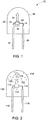
- Lighting apparatus 10 includes a semiconductor radiation source, shown as light emitting diode (LED) chip 12, and leads 14 electrically attached to the LED chip.
- the leads 14 may be thin wires supported by a thicker lead frame(s) 16 or the leads may be self supported electrodes and the lead frame may be omitted.
- the leads 14 provide current to LED chip 12 and thus cause it to emit radiation.
- the lamp may include any semiconductor blue or UV light source that is capable of producing white light when its emitted radiation is directed onto the phosphor.
- the semiconductor light source is a blue emitting LED doped with various impurities.
- the LED may comprise a semiconductor diode based on any suitable III-V, II-VI or IV-IV semiconductor layers and having an emission wavelength of about 250 to 550 nm.
- the LED may contain at least one semiconductor layer comprising GaN, ZnSe or SiC.
- the chip is a near-uv or blue emitting LED having a peak emission wavelength from about 400 to about 500 nm.
- LED semiconductors are known in the art.
- the radiation source is described herein as an LED for convenience. However, as used herein, the term is meant to encompass all semiconductor radiation sources including, e.g., semiconductor laser diodes.
- LED chip may be replaced by another radiation source unless otherwise noted and that any reference to semiconductor, semiconductor LED, or LED chip is merely representative of any appropriate radiation source, including, but not limited to, organic light emitting diodes.
- the LED chip 12 may be encapsulated within a shell 18, which encloses the LED chip and an encapsulant material 20.
- the shell 18 may be, for example, glass or plastic.
- the LED 12 is substantially centered in the encapsulant 20.
- the encapsulant 20 is preferably an epoxy, plastic, low temperature glass, polymer, thermoplastic, thermoset material, resin or other type of LED encapsulating material as is known in the art.
- the encapsulant 20 is a spin-on glass or some other high index of refraction material.
- the encapsulant material 20 is an epoxy or a polymer material, such as silicone.
- Both the shell 18 and the encapsulant 20 are preferably transparent or substantially optically transmissive with respect to the wavelength of light produced by the LED chip 12 and phosphor blend 22, which contains a Mn +4 doped phosphor according to the present invention.
- the lamp may 10 may only comprise an encapsulant material without an outer shell 18.
- the LED chip 12 may be supported, for example, by the lead frame 16, by the self supporting electrodes, the bottom of the shell 18, or by a pedestal (not shown) mounted to the shell or to the lead frame.
- the LED chip 12 is mounted in a reflective cup (not shown).
- the cup may be made from or coated with a reflective material, such as alumina, titania, or other dielectric powder known in the art, particularly alumina.
- Lighting apparatus 10 includes phosphor blend 22, radiationally coupled to the LED chip 12. Radiationally coupled means that the elements are associated with each other so radiation from one is transmitted to the other.
- Phosphor blend 22 is deposited on the LED 12 by any appropriate method. For example, a water based suspension of the phosphor(s) can be formed, and applied as a phosphor layer to the LED surface. In one such method, a silicone slurry in which the phosphor particles are randomly suspended is placed around the LED. This method is merely exemplary of possible positions of phosphor blend 22 and LED 12. Thus, phosphor blend 22 may be coated over or directly on the light emitting surface of the LED chip 12 by coating and drying the phosphor suspension over the LED chip 12.
- the median particle size of the phosphor composition ranges from about 1 to about 25 microns, particularly from about 15 to about 20 microns.
- phosphor blend 22 is interspersed within the encapsulant material 20, instead of being formed directly on the LED chip 12.
- the phosphor (in the form of a powder) may be interspersed within a single region of the encapsulant material 20 or, more preferably, throughout the entire volume of the encapsulant material. Blue light emitted by the LED chip 12 mixes with the light emitted by phosphor blend 22, and the mixed light appears as white light. If the phosphor is to be interspersed within the material of encapsulant 20, then a phosphor powder may be added to a polymer precursor, loaded around the LED chip 12, and then the polymer precursor may be cured to solidify the polymer material. Other known phosphor interspersion methods may also be used, such as transfer loading.
- phosphor blend 22 is coated onto a surface of the shell 18, instead of being formed over the LED chip 12.
- the phosphor composition is preferably coated on the inside surface of the shell 18, although the phosphor may be coated on the outside surface of the shell, if desired.
- Phosphor blend 22 may be coated on the entire surface of the shell or only a top portion of the surface of the shell.
- the UV/blue light emitted by the LED chip 12 mixes with the light emitted by phosphor blend 22, and the mixed light appears as white light.
- the phosphor may be located in any two or all three locations or in any other suitable location, such as separately from the shell or integrated into the LED.
- FIG. 2 illustrates a second structure of the system according to the present invention.
- Corresponding numbers from FIGS. 1-4 relate to corresponding structures in each of the figures, unless otherwise stated.
- the structure of the embodiment of FIG. 2 is similar to that of FIG. 1 , except that the phosphor material 122 is interspersed within the encapsulant material 120, instead of being formed directly on the LED chip 112.
- the phosphor in the form of a powder
- Radiation (indicated by arrow 126) emitted by the LED chip 112 mixes with the light emitted by the phosphor 122, and the mixed light appears as white light 124. If the phosphor is to be interspersed within the encapsulant material 120, then a phosphor powder may be added to a polymer precursor, and loaded around the LED chip 112. The polymer precursor may then be cured to solidify the polymer. Other known phosphor interspersion methods may also be used, such as transfer molding.
- FIG. 3 illustrates a third possible structure of the system according to the present invention.
- the structure of the embodiment shown in FIG. 3 is similar to that of FIG. 1 , except that the phosphor material 222 is coated onto a surface of the envelope 218, instead of being formed over the LED chip 212.
- the phosphor material 222 is preferably coated on the inside surface of the envelope 218, although the phosphor may be coated on the outside surface of the envelope, if desired.
- the phosphor 222 may be coated on the entire surface of the envelope, or only a top portion of the surface of the envelope.
- the radiation 226 emitted by the LED chip 212 mixes with the light emitted by the phosphor 222, and the mixed light appears as white light 224.
- the structures of FIGS. 1-3 may be combined, and the phosphor may be located in any two or all three locations, or in any other suitable location, such as separately from the envelope, or integrated into the LED.
- the lamp 10 ⁇ as exemplified in FIG. 1 may also include a plurality of scattering particles (not shown), which are embedded in the encapsulant material.
- the scattering particles may comprise, for example, alumina or titania. The scattering particles effectively scatter the directional light emitted from the LED chip, preferably with a negligible amount of absorption.
- the LED chip 412 may be mounted in a reflective cup 430.
- the cup 430 may be made from or coated with a reflective material, such as alumina, titania, or other dielectric powders known in the art, particularly alumina.
- the remainder of the structure of the embodiment of FIG. 4 is the same as those of any of the previous figures, and can include two leads 416, a conducting wire 432, and an encapsulant material 420.
- the reflective cup 430 is supported by the first lead 416 and the conducting wire 432 is used to electrically connect the LED chip 412 with the second lead 416.
- SMD surface mounted device
- This SMD is a "side-emitting type” and has a light-emitting window 552 on a protruding portion of a light guiding member 554.
- the SMD type light emitting diodes 550 can be made by disposing LEDs that have been formed beforehand by flow soldering or the like on a glass epoxy substrate, whereon an electrically conductive pattern has been formed and covering the LED with the window 552.
- An SMD package may comprise an LED chip as defined above, and a phosphor material that is excited by the light emitted from the LED chip.
- Lamp 10 When used with an LED emitting at from 350 to 550 nm and one or more other appropriate phosphors, the resulting lighting system will produce a light having a white color, the characteristics of which will be discussed in more detail below.
- Lamp 10 may also include scattering particles (not shown), which are embedded in the encapsulant material.
- the scattering particles may comprise, for example, alumina or titania. The scattering particles effectively scatter the directional light emitted from the LED chip, preferably with a negligible amount of absorption.
- phosphor blend 22 may include one or more other phosphors.
- the resultant light emitted by the assembly will be a white light.
- Other phosphors such as green, blue, orange, or other color phosphors may be used in the blend to customize the white color of the resulting light and produce higher CRI sources.
- the lighting apparatus When used in conjunction with a LED chip emitting at from, e.g., 250 to 550 nm, the lighting apparatus preferably includes a blue phosphor for converting some, and preferably all, of the LED radiation to blue light, which in turn can then be efficiently converted by the color stable Mn +4 phosphors and phosphor blends of the present invention.
- Suitable phosphors for use in phosphor blends according to the present invention include, but are not limited to, (Ba,Sr,Ca) 5 (PO 4 ) 3 (Cl,F,Br,OH):Eu 2+ ,Mn 2+ ; (Ba,Sr,Ca)BPO 5 :Eu 2+ ,Mn 2+ ; (Sr,Ca) 10 (PO 4 ) 6 *vB 2 O 3 :Eu 2+ (wherein 0 ⁇ v ⁇ 1); Sr 2 Si 3 O 8 *2SrCl 2 :Eu 2+ ; (Ca,Sr,Ba) 3 MgSi 2 O 8 :Eu 2+ ,Mn 2+ ; BaAl 8 O 13 :Eu 2+ ; 2SrO*0.84P 2 O 5 *0.16B 2 O 3 :Eu 2+ ; (Ba,Sr,Ca)MgAl 10 O 17 :Eu 2+ ,Mn 2+
- the ratio of each of the individual phosphors in the phosphor blend may vary depending on the characteristics of the desired light output.
- the relative proportions of the individual phosphors in the various embodiment phosphor blends may be adjusted such that when their emissions are blended and employed in an LED lighting device, there is produced visible light of predetermined x and y values on the CIE chromaticity diagram.
- a white light is preferably produced. This white light may, for instance, may possess an x value in the range of about 0.30 to about 0.55, and a y value in the range of about 0.30 to about 0.55.
- the exact identity and amounts of each phosphor in the phosphor composition can be varied according to the needs of the end user.
- a phosphor according to the present invention allows for a white LED device having a higher CRI value and lower CCT as compared to a cerium doped terbium aluminum garnet (TAG) based lighting device.
- LED devices having CCT values from about 2500 to about 10000, preferably from 2500 to 4500, and high CRI values from about 70 to 95 can be made. This allows for an increased ccx coordinate and a reduced ccy coordinate on the CIE color chromaticity diagram for the LED device, resulting in a "warmer" color LED.
- the color stable Mn +4 doped phosphors of the present invention may be used in applications other than those described above.
- the material may be used as a phosphor in a fluorescent lamp, in a cathode ray tube, in a plasma display device or in a liquid crystal display (LCD).
- the material may also be used as a scintillator in an electromagnetic calorimeter, in a gamma ray camera, in a computed tomography scanner or in a laser. These uses are merely exemplary and not limiting.
- Powders are incorporated into a two-part silicone (RTV615, Momentive) with 50-75 wt% phosphor loading. These silicone/powder composites are then poured into Al plaque holders with a small indentation and emission and reflectance (versus a BaSO 4 standard) under 450 nm excitation are measured for each sample. Some of the plaques are reserved and stored under dry nitrogen as control samples. The other plaques are aged at about 80°C at about 80% relative humidity, and after a fixed time, spectra of the exposed and control plaque intensities are re-measured. Comparison of the QE before and after aging is a measure of the degradation of the sample.
- Hydrofluoric acid 49 wt%, 79 ml was added to water (21 ml) to from a 40% HF solution in water, and then K 2 SiF 6 (10 g, 0.454 moles) was added to the HF solution.
- the solution was heated to about 70-80°C, and K 2 MnF 6 (1 g, 0.0040 moles) was added and stirred until dissolved.
- the solution was transferred to a cold bath composed of a half frozen 40 volume% isopropanol -water solution at -20°C or a half frozen 58 volume % ethylene glycol water solution for -48 C.
- the HF-phosphor slurry was filtered through a medium porosity filter paper in a plastic funnel over a plastic beaker, washed with acetone, and air dried.
- the PFS phosphor was stored under an argon atmosphere.
- a saturated solution of K 2 SiF 6 in 40% HF was prepared by adding K 2 SiF 6 to 100 mL 40% HF in until no more could be dissolved ( ⁇ 1.75 g at room temperature).
- the phosphor powder from Example 3 was then added to the saturated solution.
- the resulting slurry was held at room temperature with stirring for about 15 minutes.
- the treated phosphor was allowed to settle and the 40% HF was decanted. Residual HF was removed by washing with dry acetone. The treated phosphor was then vacuum filtered and dried.
- the phosphors of Examples 3 and 4 were subjected to the HHTH test procedure described. After about 48 hours, the untreated phosphor of Example 2 had degraded, while the treated phosphor of Example 4 showed no degradation. QE of the treated sample was initially about 15-20% higher than QE of the untreated sample. In addition, body color of the untreated PFS appeared more orange and had reduced absorption in the visible range. After the HHTH treatment, QE of the untreated phosphor was about 31-33% of the initial value, while for the treated material, QE after HHTH was about 95% of the initial value. Results are shown in Table 1. TABLE 1 Initial QE QE after 48 hrs, % Example 3 80-85 27 Example 4 100 95
Landscapes
- Chemical & Material Sciences (AREA)
- Engineering & Computer Science (AREA)
- Materials Engineering (AREA)
- Organic Chemistry (AREA)
- Inorganic Chemistry (AREA)
- Microelectronics & Electronic Packaging (AREA)
- Manufacturing & Machinery (AREA)
- Computer Hardware Design (AREA)
- Power Engineering (AREA)
- Luminescent Compositions (AREA)
- Led Device Packages (AREA)
Applications Claiming Priority (3)
| Application Number | Priority Date | Filing Date | Title |
|---|---|---|---|
| US13/069,756 US8252613B1 (en) | 2011-03-23 | 2011-03-23 | Color stable manganese-doped phosphors |
| EP12703644.0A EP2688978B1 (en) | 2011-03-23 | 2012-01-19 | Color stable manganese-doped phosphors |
| PCT/US2012/021828 WO2012128837A1 (en) | 2011-03-23 | 2012-01-19 | Color stable manganese-doped phosphors |
Related Parent Applications (2)
| Application Number | Title | Priority Date | Filing Date |
|---|---|---|---|
| EP12703644.0A Division EP2688978B1 (en) | 2011-03-23 | 2012-01-19 | Color stable manganese-doped phosphors |
| EP12703644.0A Division-Into EP2688978B1 (en) | 2011-03-23 | 2012-01-19 | Color stable manganese-doped phosphors |
Publications (2)
| Publication Number | Publication Date |
|---|---|
| EP3095832A1 EP3095832A1 (en) | 2016-11-23 |
| EP3095832B1 true EP3095832B1 (en) | 2019-08-07 |
Family
ID=45582039
Family Applications (2)
| Application Number | Title | Priority Date | Filing Date |
|---|---|---|---|
| EP12703644.0A Active EP2688978B1 (en) | 2011-03-23 | 2012-01-19 | Color stable manganese-doped phosphors |
| EP16173586.5A Active EP3095832B1 (en) | 2011-03-23 | 2012-01-19 | Color stable manganese-doped phosphors |
Family Applications Before (1)
| Application Number | Title | Priority Date | Filing Date |
|---|---|---|---|
| EP12703644.0A Active EP2688978B1 (en) | 2011-03-23 | 2012-01-19 | Color stable manganese-doped phosphors |
Country Status (6)
| Country | Link |
|---|---|
| US (2) | US8252613B1 (zh) |
| EP (2) | EP2688978B1 (zh) |
| JP (2) | JP5899304B2 (zh) |
| KR (2) | KR102024500B1 (zh) |
| CN (2) | CN103429701B (zh) |
| WO (1) | WO2012128837A1 (zh) |
Families Citing this family (116)
| Publication number | Priority date | Publication date | Assignee | Title |
|---|---|---|---|---|
| US8252613B1 (en) * | 2011-03-23 | 2012-08-28 | General Electric Company | Color stable manganese-doped phosphors |
| US9210775B2 (en) * | 2012-10-31 | 2015-12-08 | General Electric Company | Method and system for storage of perishable items |
| US9580648B2 (en) * | 2013-03-15 | 2017-02-28 | General Electric Company | Color stable red-emitting phosphors |
| US9698314B2 (en) * | 2013-03-15 | 2017-07-04 | General Electric Company | Color stable red-emitting phosphors |
| US9868898B2 (en) | 2013-03-15 | 2018-01-16 | General Electric Company | Processes for preparing color stable red-emitting phosphors |
| US20140327023A1 (en) * | 2013-05-02 | 2014-11-06 | General Electric Company | Phosphor assembly for light emitting devices |
| CN103275711B (zh) * | 2013-06-08 | 2015-06-17 | 温州大学 | 一种二基色白光led用氟钛盐红光材料及其制备方法 |
| JP5783302B2 (ja) | 2013-07-03 | 2015-09-24 | 日亜化学工業株式会社 | フッ化物蛍光体及びそれを用いた発光装置並びに蛍光体の製造方法 |
| JP5854166B2 (ja) * | 2013-07-03 | 2016-02-09 | 日亜化学工業株式会社 | フッ化物蛍光体の製造方法 |
| JP6187253B2 (ja) * | 2013-08-01 | 2017-08-30 | 日亜化学工業株式会社 | フッ化物蛍光体の製造方法 |
| US9399732B2 (en) | 2013-08-22 | 2016-07-26 | General Electric Company | Processes for preparing color stable manganese-doped phosphors |
| JP6149606B2 (ja) | 2013-08-26 | 2017-06-21 | 日亜化学工業株式会社 | フッ化物蛍光体の製造方法 |
| US11041118B2 (en) | 2013-08-29 | 2021-06-22 | Nichia Corporation | Fluoride fluorescent material and method for producing the same as well as light emitting device using the same |
| US10381527B2 (en) | 2014-02-10 | 2019-08-13 | Consumer Lighting, Llc | Enhanced color-preference LED light sources using yag, nitride, and PFS phosphors |
| CA2923187C (en) | 2013-09-09 | 2022-04-12 | GE Lighting Solutions, LLC | Enhanced color-preference light sources |
| CN103540314B (zh) * | 2013-10-10 | 2015-01-14 | 上海师范大学 | 一种低温合成的氟硅酸盐纳米棒红色荧光粉及其制备方法 |
| US20150123153A1 (en) * | 2013-11-06 | 2015-05-07 | General Electric Company | Led package with red-emitting phosphors |
| KR102122359B1 (ko) * | 2013-12-10 | 2020-06-12 | 삼성전자주식회사 | 발광장치 제조방법 |
| MY183192A (en) * | 2013-12-13 | 2021-02-18 | Gen Electric | Processes for preparing color stable manganese-doped complex fluoride phosphors |
| JPWO2015093430A1 (ja) * | 2013-12-17 | 2017-03-16 | デンカ株式会社 | 蛍光体の製造方法 |
| MY174459A (en) * | 2013-12-30 | 2020-04-20 | Gen Electric | Moisture-resistant phosphor compositions and associate methods |
| JP6119623B2 (ja) * | 2014-01-30 | 2017-04-26 | 信越化学工業株式会社 | 複フッ化物蛍光体の製造方法 |
| CN106062130A (zh) * | 2014-02-26 | 2016-10-26 | 电化株式会社 | 荧光体、发光元件及发光装置 |
| US10230022B2 (en) | 2014-03-13 | 2019-03-12 | General Electric Company | Lighting apparatus including color stable red emitting phosphors and quantum dots |
| JP6187509B2 (ja) * | 2014-03-14 | 2017-08-30 | 日亜化学工業株式会社 | 発光装置及びその製造方法 |
| JP6394742B2 (ja) * | 2014-03-14 | 2018-09-26 | 日亜化学工業株式会社 | 発光装置の製造方法 |
| US9755116B2 (en) | 2014-03-14 | 2017-09-05 | Nichia Corporation | Method of manufacturing light emitting device |
| US9590148B2 (en) | 2014-03-18 | 2017-03-07 | GE Lighting Solutions, LLC | Encapsulant modification in heavily phosphor loaded LED packages for improved stability |
| US9680067B2 (en) | 2014-03-18 | 2017-06-13 | GE Lighting Solutions, LLC | Heavily phosphor loaded LED packages having higher stability |
| JP6094522B2 (ja) * | 2014-04-10 | 2017-03-15 | 日亜化学工業株式会社 | フッ化物蛍光体の製造方法 |
| US9546318B2 (en) * | 2014-05-01 | 2017-01-17 | General Electric Company | Process for preparing red-emitting phosphors |
| US9512356B2 (en) * | 2014-05-01 | 2016-12-06 | General Electric Company | Process for preparing red-emitting phosphors |
| US9385282B2 (en) * | 2014-06-12 | 2016-07-05 | General Electric Company | Color stable red-emitting phosphors |
| US10563121B2 (en) * | 2014-06-12 | 2020-02-18 | Current Lighting Solutions, Llc | Red-emitting phosphors and associated devices |
| US9376615B2 (en) * | 2014-06-12 | 2016-06-28 | General Electric Company | Color stable red-emitting phosphors |
| US9567516B2 (en) * | 2014-06-12 | 2017-02-14 | General Electric Company | Red-emitting phosphors and associated devices |
| US9371481B2 (en) | 2014-06-12 | 2016-06-21 | General Electric Company | Color stable red-emitting phosphors |
| US9929319B2 (en) | 2014-06-13 | 2018-03-27 | General Electric Company | LED package with red-emitting phosphors |
| US9512357B2 (en) * | 2014-07-22 | 2016-12-06 | General Electric Company | Red-emitting phosphors, associated processes and devices |
| JP2017527114A (ja) * | 2014-08-11 | 2017-09-14 | ゲルト オー ミュラー | 白熱様減光発光ダイオード |
| EP3194529A1 (en) * | 2014-09-09 | 2017-07-26 | GE Lighting Solutions, LLC | Enhanced color-preference led light sources using lag, nitride and pfs phosphors |
| KR101809793B1 (ko) | 2014-09-30 | 2017-12-15 | 니치아 카가쿠 고교 가부시키가이샤 | 불화물 형광체 및 그 제조 방법 및 발광 장치 |
| US10047286B2 (en) * | 2014-10-27 | 2018-08-14 | General Electric Company | Color stable red-emitting phosphors |
| JP6303980B2 (ja) * | 2014-10-30 | 2018-04-04 | 信越化学工業株式会社 | Mn賦活複フッ化物蛍光体の処理方法 |
| KR102369932B1 (ko) | 2014-11-10 | 2022-03-04 | 삼성전자주식회사 | 불화물계 형광체, 발광장치, 불화물계 형광체 제조방법 및 발광장치 제조방법 |
| MX2017006661A (es) * | 2014-11-21 | 2017-10-04 | Gen Electric | Fosforos emisores de color rojo estable. |
| KR102337406B1 (ko) | 2014-12-09 | 2021-12-13 | 삼성전자주식회사 | 불화물 형광체, 불화물 형광체 제조방법, 백색 발광장치, 디스플레이 장치 및 조명장치 |
| US9890328B2 (en) | 2014-12-12 | 2018-02-13 | General Electric Company | Phosphor compositions and lighting apparatus thereof |
| JP6603458B2 (ja) * | 2015-02-12 | 2019-11-06 | 株式会社東芝 | 蛍光体、およびその製造方法、ならびにその蛍光体を用いた発光装置 |
| KR102408618B1 (ko) * | 2015-02-16 | 2022-06-14 | 쑤저우 레킨 세미컨덕터 컴퍼니 리미티드 | 발광 소자 패키지 및 이를 포함하는 조명 장치 |
| KR102615700B1 (ko) * | 2015-02-18 | 2023-12-19 | 덴카 주식회사 | 형광체의 제조 방법 |
| US9982190B2 (en) * | 2015-02-20 | 2018-05-29 | General Electric Company | Color stable red-emitting phosphors |
| TWI696726B (zh) | 2015-03-05 | 2020-06-21 | 美商通用電機股份有限公司 | 發紅光磷光體、彼之製法及含彼之裝置 |
| CN104861958B (zh) | 2015-05-14 | 2017-02-15 | 北京理工大学 | 一种钙钛矿/聚合物复合发光材料及其制备方法 |
| US10174248B2 (en) | 2015-05-18 | 2019-01-08 | General Electric Company | Process for improved halide materials |
| WO2016186636A1 (en) * | 2015-05-18 | 2016-11-24 | General Electric Company | Process for manufacturing mn-doped fluoride phosphors |
| CN106281320A (zh) | 2015-05-21 | 2017-01-04 | 隆达电子股份有限公司 | 荧光粉、其制备方法及包含其发光装置与背光模块 |
| WO2016195937A1 (en) | 2015-06-01 | 2016-12-08 | General Electric Company | Color stable red-emitting phosphors |
| CN106244143B (zh) | 2015-06-04 | 2019-08-27 | 隆达电子股份有限公司 | 具有优选方向的荧光粉、其制备方法及包含其的发光元件封装结构 |
| US9871173B2 (en) | 2015-06-18 | 2018-01-16 | Cree, Inc. | Light emitting devices having closely-spaced broad-spectrum and narrow-spectrum luminescent materials and related methods |
| KR102397910B1 (ko) | 2015-07-06 | 2022-05-16 | 삼성전자주식회사 | 불화물계 형광체, 불화물계 형광체 제조방법 및 발광장치 |
| KR102490444B1 (ko) * | 2015-08-07 | 2023-01-20 | 삼성디스플레이 주식회사 | 표면 개질된 형광체 및 이를 포함하는 발광 장치 |
| KR101722052B1 (ko) | 2015-08-13 | 2017-04-03 | 한국화학연구원 | 형광체의 제조방법 및 이에 따라 제조되는 형광체를 포함하는 발광소자 |
| JP6549070B2 (ja) * | 2015-09-10 | 2019-07-24 | 株式会社東芝 | 蛍光体及びその製造方法、並びに発光装置 |
| KR101854114B1 (ko) | 2015-09-23 | 2018-06-14 | 한국화학연구원 | 금속불화물 적색 형광체 및 이를 이용한 발광소자 |
| JP6545055B2 (ja) * | 2015-09-24 | 2019-07-17 | デンカ株式会社 | 蛍光体の製造方法 |
| FR3043687B1 (fr) * | 2015-11-13 | 2020-07-03 | Universite Blaise Pascal Clermont Ii | Procede sol-gel de synthese d'un materiau luminescent de formulation generale axbyfz:mn |
| TWI564367B (zh) | 2015-11-16 | 2017-01-01 | 隆達電子股份有限公司 | 氟化物螢光粉、其製備方法及包含其之發光裝置與背光模組 |
| KR101694256B1 (ko) | 2015-11-24 | 2017-01-23 | 한국화학연구원 | 금속불화물계 형광체의 연속 제조방법 |
| EP3380581B1 (en) | 2015-11-26 | 2020-07-15 | General Electric Company | Processes for synthesizing red-emitting phosphors and related red-emitting phosphors |
| TWI575058B (zh) | 2016-01-06 | 2017-03-21 | 隆達電子股份有限公司 | 螢光粉、其製備方法、調控其晶相的方法、及使其產生相轉變的方法 |
| KR102530756B1 (ko) | 2016-01-13 | 2023-05-10 | 삼성전자주식회사 | 불화물계 형광체, 불화물계 형광체 제조방법 및 발광장치 |
| JP6447557B2 (ja) * | 2016-03-24 | 2019-01-09 | 日亜化学工業株式会社 | 発光装置の製造方法 |
| US10851293B2 (en) * | 2016-04-14 | 2020-12-01 | Current Lighting Solutions, Llc | Phosphor materials for light sources and method for manufacturing the same |
| CN105950137A (zh) * | 2016-05-05 | 2016-09-21 | 中国人民大学 | 一种Mn4+掺杂的氟化物红色荧光粉及其制备方法与应用 |
| CA3022990C (en) | 2016-05-09 | 2024-02-20 | General Electric Company | Manganese-doped phosphor materials for high power density applications |
| WO2017210080A1 (en) | 2016-06-02 | 2017-12-07 | General Electric Company | Red-emitting phosphors and associated devices |
| JP2018002813A (ja) * | 2016-06-29 | 2018-01-11 | 株式会社東芝 | 蛍光体および発光装置 |
| US10072206B2 (en) | 2016-06-30 | 2018-09-11 | General Electric Company | Processes for preparing color stable red-emitting phosphors |
| US10193030B2 (en) | 2016-08-08 | 2019-01-29 | General Electric Company | Composite materials having red emitting phosphors |
| US11114591B2 (en) * | 2016-08-17 | 2021-09-07 | Current Lighting Solutions, Llc | Core-shell materials with red-emitting phosphors |
| US11702348B2 (en) | 2016-08-19 | 2023-07-18 | Current Lighting Solutions, Llc | Purified potassium hexafluoromanganate and methods for purifying potassium hexafluoromanganate |
| CN106433626B (zh) * | 2016-09-22 | 2019-02-12 | 陕西师范大学 | 一种Mn(IV)激活的氟化物红色荧光粉的制备方法 |
| CN109996856A (zh) * | 2016-10-12 | 2019-07-09 | 默克专利股份有限公司 | 用作LED固态光源转化发光体的Mn4+-活化发光材料 |
| TWI652329B (zh) | 2016-10-19 | 2019-03-01 | 隆達電子股份有限公司 | 含有片狀結晶體之氟化物螢光粉及其製造方法與應用 |
| TWI615458B (zh) | 2016-10-28 | 2018-02-21 | 隆達電子股份有限公司 | 波長轉換膜片及應用其之發光裝置與顯示器 |
| CN106566545B (zh) * | 2016-11-10 | 2018-10-30 | 云南民族大学 | 一种Mn4+激活的七氟铪酸盐红色发光材料及制备方法 |
| CN106566546B (zh) * | 2016-11-10 | 2019-08-06 | 云南民族大学 | 一种Mn4+激活的多氟化物红色发光材料及制备方法 |
| JP6799682B2 (ja) * | 2016-11-17 | 2020-12-16 | ゼネラル・エレクトリック・カンパニイ | 被覆赤色線放出蛍光体 |
| CN106634988B (zh) * | 2016-11-30 | 2019-01-08 | 中国计量大学 | 用于荧光温度探针的纳米晶材料 |
| US10731076B2 (en) * | 2016-12-01 | 2020-08-04 | Current Lighting Solutions, Llc | Processes for preparing stable red-emitting phosphors |
| JP6344460B2 (ja) * | 2016-12-12 | 2018-06-20 | 日亜化学工業株式会社 | フッ化物蛍光体の製造方法 |
| US11193059B2 (en) | 2016-12-13 | 2021-12-07 | Current Lighting Solutions, Llc | Processes for preparing color stable red-emitting phosphor particles having small particle size |
| US10793773B2 (en) | 2017-03-16 | 2020-10-06 | Current Lighting Solutions, Llc | Color stable red-emitting phosphors |
| WO2018185116A2 (de) | 2017-04-07 | 2018-10-11 | Merck Patent Gmbh | Uranyl-sensibilisierte europium-leuchtstoffe |
| CN107353899A (zh) * | 2017-06-15 | 2017-11-17 | 华南理工大学 | 一种Mn4+掺杂氟化物单晶红光材料及其制备方法与应用 |
| EP3418252B1 (en) | 2017-06-20 | 2022-11-16 | Vestel Elektronik Sanayi ve Ticaret A.S. | Quantum dot liquid lens, devices comprising the same, method of manufacturing a quantum dot liquid lens, and method of operating a light emitting electronic device |
| EP3418041A1 (en) | 2017-06-20 | 2018-12-26 | Vestel Elektronik Sanayi ve Ticaret A.S. | Quantum dot lens, devices comprising the same, and method of manufacturing a quantum dot lens |
| US20190048258A1 (en) * | 2017-08-10 | 2019-02-14 | General Electric Company | Coated manganese doped phosphors |
| CN109423276B (zh) * | 2017-09-05 | 2022-03-15 | 厦门稀土材料研究所 | 一种高效稳定的Mn4+掺杂氟化物发光材料及其制备方法 |
| WO2019054979A1 (en) | 2017-09-12 | 2019-03-21 | General Electric Company | METHODS FOR PREPARING COLOR-STABLE RED EMITTING LUMINOPHORES |
| WO2019054986A1 (en) | 2017-09-12 | 2019-03-21 | General Electric Company | METHODS FOR PREPARING PHOSPHORES EMITTING IN STABLE COLOR RED |
| TWI732041B (zh) * | 2017-09-14 | 2021-07-01 | 美商現代照明解決方案公司 | 具有發射紅光磷光體之複合材料 |
| TW201925419A (zh) | 2017-09-18 | 2019-07-01 | 德商馬克專利公司 | 作為固態光源之色彩轉換器的多組分發光團 |
| US10541353B2 (en) | 2017-11-10 | 2020-01-21 | Cree, Inc. | Light emitting devices including narrowband converters for outdoor lighting applications |
| JP2020019921A (ja) | 2018-02-06 | 2020-02-06 | 信越化学工業株式会社 | 蛍光体粒子 |
| JP7057918B2 (ja) | 2018-03-24 | 2022-04-21 | 国立大学法人 新潟大学 | 赤色フッ化物蛍光体の製造方法 |
| JP7026903B2 (ja) | 2018-03-24 | 2022-03-01 | 国立大学法人 新潟大学 | 赤色フッ化物蛍光体及びその母体結晶の製造方法 |
| US10608148B2 (en) | 2018-05-31 | 2020-03-31 | Cree, Inc. | Stabilized fluoride phosphor for light emitting diode (LED) applications |
| CN111057535A (zh) * | 2018-10-16 | 2020-04-24 | 云南民族大学 | 一种Mn4+掺杂的氟化物同质包裹的红色发光晶体制备方法 |
| CN111171815B (zh) * | 2018-11-13 | 2021-12-17 | 厦门稀土材料研究所 | 一种氟化物发光材料的表面改性方法及其制备得到的氟化物发光材料 |
| CN109777418A (zh) * | 2019-01-21 | 2019-05-21 | 温州大学 | 一种Mn4+掺杂双碱金属复合氟钛酸盐红光材料及其制备方法 |
| CN110294597B (zh) * | 2019-05-28 | 2021-01-19 | 华南农业大学 | 一种宽色域显示用铯铅溴钙钛矿量子点荧光玻璃及其制备方法和应用 |
| CN112094643B (zh) * | 2019-06-18 | 2022-03-22 | 中国科学院福建物质结构研究所 | 一种Mn4+掺杂氟化物窄带红色荧光粉及其制备方法和应用 |
| CN115698199A (zh) | 2020-04-14 | 2023-02-03 | 通用电气公司 | 具有窄带发射磷光体材料的油墨组合物和膜 |
| WO2023176559A1 (ja) * | 2022-03-15 | 2023-09-21 | デンカ株式会社 | 複フッ化物蛍光体の製造方法 |
Family Cites Families (17)
| Publication number | Priority date | Publication date | Assignee | Title |
|---|---|---|---|---|
| GB1360690A (en) | 1973-02-16 | 1974-07-17 | Gen Electric Co Ltd | Luminescent materials |
| US6346326B1 (en) * | 1998-10-15 | 2002-02-12 | Sarnoff Corporation | Coated moisture impervious red phosphors |
| JP4628643B2 (ja) * | 2002-08-30 | 2011-02-09 | パナソニック株式会社 | プラズマディスプレイパネルおよび蛍光体 |
| US7648649B2 (en) * | 2005-02-02 | 2010-01-19 | Lumination Llc | Red line emitting phosphors for use in led applications |
| US7497973B2 (en) | 2005-02-02 | 2009-03-03 | Lumination Llc | Red line emitting phosphor materials for use in LED applications |
| US7358542B2 (en) | 2005-02-02 | 2008-04-15 | Lumination Llc | Red emitting phosphor materials for use in LED and LCD applications |
| JP2007103052A (ja) * | 2005-09-30 | 2007-04-19 | Matsushita Electric Ind Co Ltd | プラズマディスプレイパネル |
| EP2148910B1 (en) * | 2007-04-20 | 2010-12-08 | Philips Intellectual Property & Standards GmbH | White emitting light source and luminescent material with improved colour stability |
| US7847309B2 (en) | 2007-07-16 | 2010-12-07 | GE Lighting Solutions, LLC | Red line emitting complex fluoride phosphors activated with Mn4+ |
| EP3045965B1 (en) | 2008-02-07 | 2020-05-27 | Mitsubishi Chemical Corporation | Red emitting fluoride phosphor activated by mn4+ |
| WO2009119486A1 (ja) * | 2008-03-25 | 2009-10-01 | 国立大学法人群馬大学 | 蛍光体及びその製造方法並びに該蛍光体を用いた白色発光ダイオード |
| JP2009280763A (ja) * | 2008-05-26 | 2009-12-03 | Sharp Corp | 蛍光体調製物およびそれを用いた発光装置 |
| JP5682104B2 (ja) | 2008-09-05 | 2015-03-11 | 三菱化学株式会社 | 蛍光体及びその製造方法と、その蛍光体を用いた蛍光体含有組成物及び発光装置、並びに、その発光装置を用いた画像表示装置及び照明装置 |
| JP2010093132A (ja) | 2008-10-09 | 2010-04-22 | Sharp Corp | 半導体発光装置およびそれを用いた画像表示装置、液晶表示装置 |
| JP5446511B2 (ja) | 2009-06-30 | 2014-03-19 | 三菱化学株式会社 | 蛍光体及びその製造方法と、その蛍光体を用いた蛍光体含有組成物及び発光装置、並びに、その発光装置を用いた画像表示装置及び照明装置 |
| US8057706B1 (en) * | 2010-07-27 | 2011-11-15 | General Electric Company | Moisture-resistant phosphor and associated method |
| US8252613B1 (en) * | 2011-03-23 | 2012-08-28 | General Electric Company | Color stable manganese-doped phosphors |
-
2011
- 2011-03-23 US US13/069,756 patent/US8252613B1/en active Active
-
2012
- 2012-01-19 CN CN201280014622.9A patent/CN103429701B/zh active Active
- 2012-01-19 CN CN201510183798.2A patent/CN104893718B/zh active Active
- 2012-01-19 JP JP2014501065A patent/JP5899304B2/ja active Active
- 2012-01-19 KR KR1020187031468A patent/KR102024500B1/ko active IP Right Grant
- 2012-01-19 WO PCT/US2012/021828 patent/WO2012128837A1/en active Application Filing
- 2012-01-19 EP EP12703644.0A patent/EP2688978B1/en active Active
- 2012-01-19 EP EP16173586.5A patent/EP3095832B1/en active Active
- 2012-01-19 KR KR1020137027761A patent/KR101915217B1/ko active Application Filing
- 2012-07-30 US US13/561,192 patent/US8710487B2/en active Active
-
2015
- 2015-11-10 JP JP2015219998A patent/JP6216761B2/ja active Active
Non-Patent Citations (1)
| Title |
|---|
| None * |
Also Published As
| Publication number | Publication date |
|---|---|
| CN104893718A (zh) | 2015-09-09 |
| EP3095832A1 (en) | 2016-11-23 |
| KR102024500B1 (ko) | 2019-09-23 |
| JP6216761B2 (ja) | 2017-10-18 |
| CN103429701B (zh) | 2016-04-27 |
| US8710487B2 (en) | 2014-04-29 |
| CN103429701A (zh) | 2013-12-04 |
| CN104893718B (zh) | 2018-04-10 |
| KR101915217B1 (ko) | 2018-11-08 |
| KR20180121687A (ko) | 2018-11-07 |
| JP2014514388A (ja) | 2014-06-19 |
| JP5899304B2 (ja) | 2016-04-06 |
| EP2688978A1 (en) | 2014-01-29 |
| US20120299466A1 (en) | 2012-11-29 |
| EP2688978B1 (en) | 2016-08-10 |
| JP2016053178A (ja) | 2016-04-14 |
| WO2012128837A1 (en) | 2012-09-27 |
| US8252613B1 (en) | 2012-08-28 |
| KR20140019400A (ko) | 2014-02-14 |
Similar Documents
| Publication | Publication Date | Title |
|---|---|---|
| EP3095832B1 (en) | Color stable manganese-doped phosphors | |
| KR101731741B1 (ko) | Led 용도에 사용되는 적색선 방출 인광체 | |
| US7497973B2 (en) | Red line emitting phosphor materials for use in LED applications | |
| JP2014514388A5 (zh) | ||
| TWI429731B (zh) | 由4價錳離子活化之發紅光錯合氟化磷光體 | |
| JP2005264160A (ja) | 蛍光体及びその製造方法並びにそれを用いた発光装置 | |
| WO2007120216A2 (en) | Charge compensated nitride phosphors for use in lighting applications | |
| WO2006113656A1 (en) | Red phosphor for led based lighting | |
| EP2128219A1 (en) | Fluorescent substance, method for production thereof, and wavelength converter, light-emitting device and lighting device | |
| US8308982B2 (en) | Alkaline and alkaline earth metal phosphate halides and phosphors | |
| WO2006094139A2 (en) | Oxynitride phosphors for use in lighting applications having improved color quality | |
| US8440104B2 (en) | Kimzeyite garnet phosphors | |
| US20110127905A1 (en) | Alkaline earth borate phosphors | |
| Lyons et al. | Color stable manganese-doped phosphors | |
| Lyons et al. | Color stable manganese-doped phosphors |
Legal Events
| Date | Code | Title | Description |
|---|---|---|---|
| PUAI | Public reference made under article 153(3) epc to a published international application that has entered the european phase |
Free format text: ORIGINAL CODE: 0009012 |
|
| AC | Divisional application: reference to earlier application |
Ref document number: 2688978 Country of ref document: EP Kind code of ref document: P |
|
| AK | Designated contracting states |
Kind code of ref document: A1 Designated state(s): AL AT BE BG CH CY CZ DE DK EE ES FI FR GB GR HR HU IE IS IT LI LT LU LV MC MK MT NL NO PL PT RO RS SE SI SK SM TR |
|
| STAA | Information on the status of an ep patent application or granted ep patent |
Free format text: STATUS: REQUEST FOR EXAMINATION WAS MADE |
|
| 17P | Request for examination filed |
Effective date: 20170523 |
|
| RBV | Designated contracting states (corrected) |
Designated state(s): AL AT BE BG CH CY CZ DE DK EE ES FI FR GB GR HR HU IE IS IT LI LT LU LV MC MK MT NL NO PL PT RO RS SE SI SK SM TR |
|
| STAA | Information on the status of an ep patent application or granted ep patent |
Free format text: STATUS: EXAMINATION IS IN PROGRESS |
|
| 17Q | First examination report despatched |
Effective date: 20170710 |
|
| GRAP | Despatch of communication of intention to grant a patent |
Free format text: ORIGINAL CODE: EPIDOSNIGR1 |
|
| STAA | Information on the status of an ep patent application or granted ep patent |
Free format text: STATUS: GRANT OF PATENT IS INTENDED |
|
| RIC1 | Information provided on ipc code assigned before grant |
Ipc: H01L 33/50 20100101ALN20190115BHEP Ipc: C09K 11/61 20060101AFI20190115BHEP |
|
| INTG | Intention to grant announced |
Effective date: 20190205 |
|
| GRAJ | Information related to disapproval of communication of intention to grant by the applicant or resumption of examination proceedings by the epo deleted |
Free format text: ORIGINAL CODE: EPIDOSDIGR1 |
|
| STAA | Information on the status of an ep patent application or granted ep patent |
Free format text: STATUS: EXAMINATION IS IN PROGRESS |
|
| GRAR | Information related to intention to grant a patent recorded |
Free format text: ORIGINAL CODE: EPIDOSNIGR71 |
|
| GRAS | Grant fee paid |
Free format text: ORIGINAL CODE: EPIDOSNIGR3 |
|
| STAA | Information on the status of an ep patent application or granted ep patent |
Free format text: STATUS: GRANT OF PATENT IS INTENDED |
|
| GRAA | (expected) grant |
Free format text: ORIGINAL CODE: 0009210 |
|
| STAA | Information on the status of an ep patent application or granted ep patent |
Free format text: STATUS: THE PATENT HAS BEEN GRANTED |
|
| INTC | Intention to grant announced (deleted) | ||
| RIC1 | Information provided on ipc code assigned before grant |
Ipc: C09K 11/61 20060101AFI20190618BHEP Ipc: H01L 33/50 20100101ALN20190618BHEP |
|
| AC | Divisional application: reference to earlier application |
Ref document number: 2688978 Country of ref document: EP Kind code of ref document: P |
|
| AK | Designated contracting states |
Kind code of ref document: B1 Designated state(s): AL AT BE BG CH CY CZ DE DK EE ES FI FR GB GR HR HU IE IS IT LI LT LU LV MC MK MT NL NO PL PT RO RS SE SI SK SM TR |
|
| INTG | Intention to grant announced |
Effective date: 20190701 |
|
| REG | Reference to a national code |
Ref country code: GB Ref legal event code: FG4D |
|
| REG | Reference to a national code |
Ref country code: CH Ref legal event code: EP Ref country code: AT Ref legal event code: REF Ref document number: 1163850 Country of ref document: AT Kind code of ref document: T Effective date: 20190815 |
|
| REG | Reference to a national code |
Ref country code: DE Ref legal event code: R096 Ref document number: 602012062858 Country of ref document: DE |
|
| REG | Reference to a national code |
Ref country code: IE Ref legal event code: FG4D |
|
| REG | Reference to a national code |
Ref country code: NL Ref legal event code: FP |
|
| REG | Reference to a national code |
Ref country code: LT Ref legal event code: MG4D |
|
| PG25 | Lapsed in a contracting state [announced via postgrant information from national office to epo] |
Ref country code: PT Free format text: LAPSE BECAUSE OF FAILURE TO SUBMIT A TRANSLATION OF THE DESCRIPTION OR TO PAY THE FEE WITHIN THE PRESCRIBED TIME-LIMIT Effective date: 20191209 Ref country code: BG Free format text: LAPSE BECAUSE OF FAILURE TO SUBMIT A TRANSLATION OF THE DESCRIPTION OR TO PAY THE FEE WITHIN THE PRESCRIBED TIME-LIMIT Effective date: 20191107 Ref country code: LT Free format text: LAPSE BECAUSE OF FAILURE TO SUBMIT A TRANSLATION OF THE DESCRIPTION OR TO PAY THE FEE WITHIN THE PRESCRIBED TIME-LIMIT Effective date: 20190807 Ref country code: SE Free format text: LAPSE BECAUSE OF FAILURE TO SUBMIT A TRANSLATION OF THE DESCRIPTION OR TO PAY THE FEE WITHIN THE PRESCRIBED TIME-LIMIT Effective date: 20190807 Ref country code: NO Free format text: LAPSE BECAUSE OF FAILURE TO SUBMIT A TRANSLATION OF THE DESCRIPTION OR TO PAY THE FEE WITHIN THE PRESCRIBED TIME-LIMIT Effective date: 20191107 Ref country code: HR Free format text: LAPSE BECAUSE OF FAILURE TO SUBMIT A TRANSLATION OF THE DESCRIPTION OR TO PAY THE FEE WITHIN THE PRESCRIBED TIME-LIMIT Effective date: 20190807 Ref country code: FI Free format text: LAPSE BECAUSE OF FAILURE TO SUBMIT A TRANSLATION OF THE DESCRIPTION OR TO PAY THE FEE WITHIN THE PRESCRIBED TIME-LIMIT Effective date: 20190807 |
|
| REG | Reference to a national code |
Ref country code: AT Ref legal event code: MK05 Ref document number: 1163850 Country of ref document: AT Kind code of ref document: T Effective date: 20190807 |
|
| PG25 | Lapsed in a contracting state [announced via postgrant information from national office to epo] |
Ref country code: LV Free format text: LAPSE BECAUSE OF FAILURE TO SUBMIT A TRANSLATION OF THE DESCRIPTION OR TO PAY THE FEE WITHIN THE PRESCRIBED TIME-LIMIT Effective date: 20190807 Ref country code: IS Free format text: LAPSE BECAUSE OF FAILURE TO SUBMIT A TRANSLATION OF THE DESCRIPTION OR TO PAY THE FEE WITHIN THE PRESCRIBED TIME-LIMIT Effective date: 20191207 Ref country code: GR Free format text: LAPSE BECAUSE OF FAILURE TO SUBMIT A TRANSLATION OF THE DESCRIPTION OR TO PAY THE FEE WITHIN THE PRESCRIBED TIME-LIMIT Effective date: 20191108 Ref country code: RS Free format text: LAPSE BECAUSE OF FAILURE TO SUBMIT A TRANSLATION OF THE DESCRIPTION OR TO PAY THE FEE WITHIN THE PRESCRIBED TIME-LIMIT Effective date: 20190807 Ref country code: ES Free format text: LAPSE BECAUSE OF FAILURE TO SUBMIT A TRANSLATION OF THE DESCRIPTION OR TO PAY THE FEE WITHIN THE PRESCRIBED TIME-LIMIT Effective date: 20190807 Ref country code: AL Free format text: LAPSE BECAUSE OF FAILURE TO SUBMIT A TRANSLATION OF THE DESCRIPTION OR TO PAY THE FEE WITHIN THE PRESCRIBED TIME-LIMIT Effective date: 20190807 |
|
| PG25 | Lapsed in a contracting state [announced via postgrant information from national office to epo] |
Ref country code: TR Free format text: LAPSE BECAUSE OF FAILURE TO SUBMIT A TRANSLATION OF THE DESCRIPTION OR TO PAY THE FEE WITHIN THE PRESCRIBED TIME-LIMIT Effective date: 20190807 |
|
| PG25 | Lapsed in a contracting state [announced via postgrant information from national office to epo] |
Ref country code: RO Free format text: LAPSE BECAUSE OF FAILURE TO SUBMIT A TRANSLATION OF THE DESCRIPTION OR TO PAY THE FEE WITHIN THE PRESCRIBED TIME-LIMIT Effective date: 20190807 Ref country code: EE Free format text: LAPSE BECAUSE OF FAILURE TO SUBMIT A TRANSLATION OF THE DESCRIPTION OR TO PAY THE FEE WITHIN THE PRESCRIBED TIME-LIMIT Effective date: 20190807 Ref country code: AT Free format text: LAPSE BECAUSE OF FAILURE TO SUBMIT A TRANSLATION OF THE DESCRIPTION OR TO PAY THE FEE WITHIN THE PRESCRIBED TIME-LIMIT Effective date: 20190807 Ref country code: DK Free format text: LAPSE BECAUSE OF FAILURE TO SUBMIT A TRANSLATION OF THE DESCRIPTION OR TO PAY THE FEE WITHIN THE PRESCRIBED TIME-LIMIT Effective date: 20190807 Ref country code: IT Free format text: LAPSE BECAUSE OF FAILURE TO SUBMIT A TRANSLATION OF THE DESCRIPTION OR TO PAY THE FEE WITHIN THE PRESCRIBED TIME-LIMIT Effective date: 20190807 Ref country code: PL Free format text: LAPSE BECAUSE OF FAILURE TO SUBMIT A TRANSLATION OF THE DESCRIPTION OR TO PAY THE FEE WITHIN THE PRESCRIBED TIME-LIMIT Effective date: 20190807 |
|
| PG25 | Lapsed in a contracting state [announced via postgrant information from national office to epo] |
Ref country code: CZ Free format text: LAPSE BECAUSE OF FAILURE TO SUBMIT A TRANSLATION OF THE DESCRIPTION OR TO PAY THE FEE WITHIN THE PRESCRIBED TIME-LIMIT Effective date: 20190807 Ref country code: SK Free format text: LAPSE BECAUSE OF FAILURE TO SUBMIT A TRANSLATION OF THE DESCRIPTION OR TO PAY THE FEE WITHIN THE PRESCRIBED TIME-LIMIT Effective date: 20190807 Ref country code: SM Free format text: LAPSE BECAUSE OF FAILURE TO SUBMIT A TRANSLATION OF THE DESCRIPTION OR TO PAY THE FEE WITHIN THE PRESCRIBED TIME-LIMIT Effective date: 20190807 Ref country code: IS Free format text: LAPSE BECAUSE OF FAILURE TO SUBMIT A TRANSLATION OF THE DESCRIPTION OR TO PAY THE FEE WITHIN THE PRESCRIBED TIME-LIMIT Effective date: 20200224 |
|
| REG | Reference to a national code |
Ref country code: DE Ref legal event code: R097 Ref document number: 602012062858 Country of ref document: DE |
|
| PLBE | No opposition filed within time limit |
Free format text: ORIGINAL CODE: 0009261 |
|
| STAA | Information on the status of an ep patent application or granted ep patent |
Free format text: STATUS: NO OPPOSITION FILED WITHIN TIME LIMIT |
|
| PG2D | Information on lapse in contracting state deleted |
Ref country code: IS |
|
| 26N | No opposition filed |
Effective date: 20200603 |
|
| PG25 | Lapsed in a contracting state [announced via postgrant information from national office to epo] |
Ref country code: MC Free format text: LAPSE BECAUSE OF FAILURE TO SUBMIT A TRANSLATION OF THE DESCRIPTION OR TO PAY THE FEE WITHIN THE PRESCRIBED TIME-LIMIT Effective date: 20190807 Ref country code: SI Free format text: LAPSE BECAUSE OF FAILURE TO SUBMIT A TRANSLATION OF THE DESCRIPTION OR TO PAY THE FEE WITHIN THE PRESCRIBED TIME-LIMIT Effective date: 20190807 |
|
| REG | Reference to a national code |
Ref country code: CH Ref legal event code: PL |
|
| GBPC | Gb: european patent ceased through non-payment of renewal fee |
Effective date: 20200119 |
|
| REG | Reference to a national code |
Ref country code: BE Ref legal event code: MM Effective date: 20200131 |
|
| PG25 | Lapsed in a contracting state [announced via postgrant information from national office to epo] |
Ref country code: FR Free format text: LAPSE BECAUSE OF NON-PAYMENT OF DUE FEES Effective date: 20200131 Ref country code: GB Free format text: LAPSE BECAUSE OF NON-PAYMENT OF DUE FEES Effective date: 20200119 Ref country code: LU Free format text: LAPSE BECAUSE OF NON-PAYMENT OF DUE FEES Effective date: 20200119 |
|
| PG25 | Lapsed in a contracting state [announced via postgrant information from national office to epo] |
Ref country code: LI Free format text: LAPSE BECAUSE OF NON-PAYMENT OF DUE FEES Effective date: 20200131 Ref country code: CH Free format text: LAPSE BECAUSE OF NON-PAYMENT OF DUE FEES Effective date: 20200131 Ref country code: BE Free format text: LAPSE BECAUSE OF NON-PAYMENT OF DUE FEES Effective date: 20200131 |
|
| PG25 | Lapsed in a contracting state [announced via postgrant information from national office to epo] |
Ref country code: IE Free format text: LAPSE BECAUSE OF NON-PAYMENT OF DUE FEES Effective date: 20200119 |
|
| PG25 | Lapsed in a contracting state [announced via postgrant information from national office to epo] |
Ref country code: MT Free format text: LAPSE BECAUSE OF FAILURE TO SUBMIT A TRANSLATION OF THE DESCRIPTION OR TO PAY THE FEE WITHIN THE PRESCRIBED TIME-LIMIT Effective date: 20190807 Ref country code: CY Free format text: LAPSE BECAUSE OF FAILURE TO SUBMIT A TRANSLATION OF THE DESCRIPTION OR TO PAY THE FEE WITHIN THE PRESCRIBED TIME-LIMIT Effective date: 20190807 |
|
| PG25 | Lapsed in a contracting state [announced via postgrant information from national office to epo] |
Ref country code: MK Free format text: LAPSE BECAUSE OF FAILURE TO SUBMIT A TRANSLATION OF THE DESCRIPTION OR TO PAY THE FEE WITHIN THE PRESCRIBED TIME-LIMIT Effective date: 20190807 |
|
| P01 | Opt-out of the competence of the unified patent court (upc) registered |
Effective date: 20230518 |
|
| PGFP | Annual fee paid to national office [announced via postgrant information from national office to epo] |
Ref country code: NL Payment date: 20231219 Year of fee payment: 13 |
|
| PGFP | Annual fee paid to national office [announced via postgrant information from national office to epo] |
Ref country code: DE Payment date: 20231219 Year of fee payment: 13 |