EP3063008B1 - Encapsulating a bonded wire with low profile encapsulation - Google Patents
Encapsulating a bonded wire with low profile encapsulation Download PDFInfo
- Publication number
- EP3063008B1 EP3063008B1 EP13896622.1A EP13896622A EP3063008B1 EP 3063008 B1 EP3063008 B1 EP 3063008B1 EP 13896622 A EP13896622 A EP 13896622A EP 3063008 B1 EP3063008 B1 EP 3063008B1
- Authority
- EP
- European Patent Office
- Prior art keywords
- encapsulation
- guide
- wire
- shape
- die
- Prior art date
- Legal status (The legal status is an assumption and is not a legal conclusion. Google has not performed a legal analysis and makes no representation as to the accuracy of the status listed.)
- Active
Links
- 238000005538 encapsulation Methods 0.000 title claims description 116
- 239000000463 material Substances 0.000 claims description 50
- 238000000034 method Methods 0.000 claims description 28
- 238000000151 deposition Methods 0.000 claims description 4
- 239000007788 liquid Substances 0.000 description 35
- 239000011347 resin Substances 0.000 description 35
- 229920005989 resin Polymers 0.000 description 35
- 230000007246 mechanism Effects 0.000 description 15
- 230000008569 process Effects 0.000 description 15
- 150000001875 compounds Chemical class 0.000 description 8
- 238000010586 diagram Methods 0.000 description 8
- RYGMFSIKBFXOCR-UHFFFAOYSA-N Copper Chemical compound [Cu] RYGMFSIKBFXOCR-UHFFFAOYSA-N 0.000 description 6
- 239000011248 coating agent Substances 0.000 description 6
- 238000000576 coating method Methods 0.000 description 6
- 238000000227 grinding Methods 0.000 description 6
- 238000001816 cooling Methods 0.000 description 4
- 239000008393 encapsulating agent Substances 0.000 description 4
- 239000004593 Epoxy Substances 0.000 description 3
- 239000000853 adhesive Substances 0.000 description 3
- 230000001070 adhesive effect Effects 0.000 description 3
- 230000008901 benefit Effects 0.000 description 3
- 238000007906 compression Methods 0.000 description 3
- PCHJSUWPFVWCPO-UHFFFAOYSA-N gold Chemical compound [Au] PCHJSUWPFVWCPO-UHFFFAOYSA-N 0.000 description 3
- 229910052737 gold Inorganic materials 0.000 description 3
- 239000010931 gold Substances 0.000 description 3
- 238000004519 manufacturing process Methods 0.000 description 3
- 239000004033 plastic Substances 0.000 description 3
- 229920003023 plastic Polymers 0.000 description 3
- 229920000642 polymer Polymers 0.000 description 3
- 239000004065 semiconductor Substances 0.000 description 3
- 229910052710 silicon Inorganic materials 0.000 description 3
- 239000010703 silicon Substances 0.000 description 3
- 125000006850 spacer group Chemical group 0.000 description 3
- 239000000758 substrate Substances 0.000 description 3
- PXHVJJICTQNCMI-UHFFFAOYSA-N Nickel Chemical compound [Ni] PXHVJJICTQNCMI-UHFFFAOYSA-N 0.000 description 2
- 230000009471 action Effects 0.000 description 2
- 229910052782 aluminium Inorganic materials 0.000 description 2
- XAGFODPZIPBFFR-UHFFFAOYSA-N aluminium Chemical compound [Al] XAGFODPZIPBFFR-UHFFFAOYSA-N 0.000 description 2
- 239000000919 ceramic Substances 0.000 description 2
- 230000006835 compression Effects 0.000 description 2
- 229910052802 copper Inorganic materials 0.000 description 2
- 239000010949 copper Substances 0.000 description 2
- 238000005260 corrosion Methods 0.000 description 2
- 230000007797 corrosion Effects 0.000 description 2
- 230000003993 interaction Effects 0.000 description 2
- -1 polyethylene terephthalate Polymers 0.000 description 2
- 238000000518 rheometry Methods 0.000 description 2
- 229910052709 silver Inorganic materials 0.000 description 2
- 239000004332 silver Substances 0.000 description 2
- BQCADISMDOOEFD-UHFFFAOYSA-N Silver Chemical compound [Ag] BQCADISMDOOEFD-UHFFFAOYSA-N 0.000 description 1
- 238000000137 annealing Methods 0.000 description 1
- 239000011324 bead Substances 0.000 description 1
- 229910052790 beryllium Inorganic materials 0.000 description 1
- ATBAMAFKBVZNFJ-UHFFFAOYSA-N beryllium atom Chemical compound [Be] ATBAMAFKBVZNFJ-UHFFFAOYSA-N 0.000 description 1
- 238000011109 contamination Methods 0.000 description 1
- 238000005336 cracking Methods 0.000 description 1
- 230000000593 degrading effect Effects 0.000 description 1
- 230000000994 depressogenic effect Effects 0.000 description 1
- 238000010304 firing Methods 0.000 description 1
- 239000012530 fluid Substances 0.000 description 1
- 238000005304 joining Methods 0.000 description 1
- 238000001459 lithography Methods 0.000 description 1
- 229910052751 metal Inorganic materials 0.000 description 1
- 239000002184 metal Substances 0.000 description 1
- 150000002739 metals Chemical class 0.000 description 1
- 238000004377 microelectronic Methods 0.000 description 1
- 229910052759 nickel Inorganic materials 0.000 description 1
- 230000003287 optical effect Effects 0.000 description 1
- 238000000206 photolithography Methods 0.000 description 1
- 229920000139 polyethylene terephthalate Polymers 0.000 description 1
- 239000005020 polyethylene terephthalate Substances 0.000 description 1
- 229920001296 polysiloxane Polymers 0.000 description 1
- 229920001343 polytetrafluoroethylene Polymers 0.000 description 1
- 239000004810 polytetrafluoroethylene Substances 0.000 description 1
- 229920002635 polyurethane Polymers 0.000 description 1
- 239000004814 polyurethane Substances 0.000 description 1
- 230000000717 retained effect Effects 0.000 description 1
- 239000000523 sample Substances 0.000 description 1
- 238000007493 shaping process Methods 0.000 description 1
- 239000007921 spray Substances 0.000 description 1
- 238000005507 spraying Methods 0.000 description 1
- 229920001187 thermosetting polymer Polymers 0.000 description 1
Images


Classifications
-
- B—PERFORMING OPERATIONS; TRANSPORTING
- B41—PRINTING; LINING MACHINES; TYPEWRITERS; STAMPS
- B41J—TYPEWRITERS; SELECTIVE PRINTING MECHANISMS, i.e. MECHANISMS PRINTING OTHERWISE THAN FROM A FORME; CORRECTION OF TYPOGRAPHICAL ERRORS
- B41J2/00—Typewriters or selective printing mechanisms characterised by the printing or marking process for which they are designed
- B41J2/005—Typewriters or selective printing mechanisms characterised by the printing or marking process for which they are designed characterised by bringing liquid or particles selectively into contact with a printing material
- B41J2/01—Ink jet
- B41J2/135—Nozzles
- B41J2/14—Structure thereof only for on-demand ink jet heads
- B41J2/1433—Structure of nozzle plates
-
- B—PERFORMING OPERATIONS; TRANSPORTING
- B41—PRINTING; LINING MACHINES; TYPEWRITERS; STAMPS
- B41J—TYPEWRITERS; SELECTIVE PRINTING MECHANISMS, i.e. MECHANISMS PRINTING OTHERWISE THAN FROM A FORME; CORRECTION OF TYPOGRAPHICAL ERRORS
- B41J2/00—Typewriters or selective printing mechanisms characterised by the printing or marking process for which they are designed
- B41J2/005—Typewriters or selective printing mechanisms characterised by the printing or marking process for which they are designed characterised by bringing liquid or particles selectively into contact with a printing material
- B41J2/01—Ink jet
- B41J2/135—Nozzles
- B41J2/14—Structure thereof only for on-demand ink jet heads
- B41J2/14016—Structure of bubble jet print heads
- B41J2/14024—Assembling head parts
-
- B—PERFORMING OPERATIONS; TRANSPORTING
- B41—PRINTING; LINING MACHINES; TYPEWRITERS; STAMPS
- B41J—TYPEWRITERS; SELECTIVE PRINTING MECHANISMS, i.e. MECHANISMS PRINTING OTHERWISE THAN FROM A FORME; CORRECTION OF TYPOGRAPHICAL ERRORS
- B41J2/00—Typewriters or selective printing mechanisms characterised by the printing or marking process for which they are designed
- B41J2/005—Typewriters or selective printing mechanisms characterised by the printing or marking process for which they are designed characterised by bringing liquid or particles selectively into contact with a printing material
- B41J2/01—Ink jet
- B41J2/135—Nozzles
- B41J2/14—Structure thereof only for on-demand ink jet heads
- B41J2/14016—Structure of bubble jet print heads
- B41J2/14072—Electrical connections, e.g. details on electrodes, connecting the chip to the outside...
-
- B—PERFORMING OPERATIONS; TRANSPORTING
- B41—PRINTING; LINING MACHINES; TYPEWRITERS; STAMPS
- B41J—TYPEWRITERS; SELECTIVE PRINTING MECHANISMS, i.e. MECHANISMS PRINTING OTHERWISE THAN FROM A FORME; CORRECTION OF TYPOGRAPHICAL ERRORS
- B41J2/00—Typewriters or selective printing mechanisms characterised by the printing or marking process for which they are designed
- B41J2/005—Typewriters or selective printing mechanisms characterised by the printing or marking process for which they are designed characterised by bringing liquid or particles selectively into contact with a printing material
- B41J2/01—Ink jet
- B41J2/135—Nozzles
- B41J2/16—Production of nozzles
- B41J2/1601—Production of bubble jet print heads
-
- B—PERFORMING OPERATIONS; TRANSPORTING
- B41—PRINTING; LINING MACHINES; TYPEWRITERS; STAMPS
- B41J—TYPEWRITERS; SELECTIVE PRINTING MECHANISMS, i.e. MECHANISMS PRINTING OTHERWISE THAN FROM A FORME; CORRECTION OF TYPOGRAPHICAL ERRORS
- B41J2/00—Typewriters or selective printing mechanisms characterised by the printing or marking process for which they are designed
- B41J2/005—Typewriters or selective printing mechanisms characterised by the printing or marking process for which they are designed characterised by bringing liquid or particles selectively into contact with a printing material
- B41J2/01—Ink jet
- B41J2/135—Nozzles
- B41J2/16—Production of nozzles
- B41J2/1621—Manufacturing processes
- B41J2/1623—Manufacturing processes bonding and adhesion
-
- H—ELECTRICITY
- H01—ELECTRIC ELEMENTS
- H01L—SEMICONDUCTOR DEVICES NOT COVERED BY CLASS H10
- H01L21/00—Processes or apparatus adapted for the manufacture or treatment of semiconductor or solid state devices or of parts thereof
- H01L21/02—Manufacture or treatment of semiconductor devices or of parts thereof
- H01L21/04—Manufacture or treatment of semiconductor devices or of parts thereof the devices having at least one potential-jump barrier or surface barrier, e.g. PN junction, depletion layer or carrier concentration layer
- H01L21/50—Assembly of semiconductor devices using processes or apparatus not provided for in a single one of the subgroups H01L21/06 - H01L21/326, e.g. sealing of a cap to a base of a container
- H01L21/56—Encapsulations, e.g. encapsulation layers, coatings
-
- H—ELECTRICITY
- H01—ELECTRIC ELEMENTS
- H01L—SEMICONDUCTOR DEVICES NOT COVERED BY CLASS H10
- H01L21/00—Processes or apparatus adapted for the manufacture or treatment of semiconductor or solid state devices or of parts thereof
- H01L21/67—Apparatus specially adapted for handling semiconductor or electric solid state devices during manufacture or treatment thereof; Apparatus specially adapted for handling wafers during manufacture or treatment of semiconductor or electric solid state devices or components ; Apparatus not specifically provided for elsewhere
- H01L21/67005—Apparatus not specifically provided for elsewhere
- H01L21/67011—Apparatus for manufacture or treatment
- H01L21/67126—Apparatus for sealing, encapsulating, glassing, decapsulating or the like
-
- H—ELECTRICITY
- H01—ELECTRIC ELEMENTS
- H01L—SEMICONDUCTOR DEVICES NOT COVERED BY CLASS H10
- H01L24/00—Arrangements for connecting or disconnecting semiconductor or solid-state bodies; Methods or apparatus related thereto
- H01L24/80—Methods for connecting semiconductor or other solid state bodies using means for bonding being attached to, or being formed on, the surface to be connected
- H01L24/85—Methods for connecting semiconductor or other solid state bodies using means for bonding being attached to, or being formed on, the surface to be connected using a wire connector
-
- H—ELECTRICITY
- H01—ELECTRIC ELEMENTS
- H01L—SEMICONDUCTOR DEVICES NOT COVERED BY CLASS H10
- H01L2224/00—Indexing scheme for arrangements for connecting or disconnecting semiconductor or solid-state bodies and methods related thereto as covered by H01L24/00
- H01L2224/01—Means for bonding being attached to, or being formed on, the surface to be connected, e.g. chip-to-package, die-attach, "first-level" interconnects; Manufacturing methods related thereto
- H01L2224/42—Wire connectors; Manufacturing methods related thereto
- H01L2224/43—Manufacturing methods
- H01L2224/438—Post-treatment of the connector
- H01L2224/4382—Applying permanent coating, e.g. in-situ coating
-
- H—ELECTRICITY
- H01—ELECTRIC ELEMENTS
- H01L—SEMICONDUCTOR DEVICES NOT COVERED BY CLASS H10
- H01L2224/00—Indexing scheme for arrangements for connecting or disconnecting semiconductor or solid-state bodies and methods related thereto as covered by H01L24/00
- H01L2224/01—Means for bonding being attached to, or being formed on, the surface to be connected, e.g. chip-to-package, die-attach, "first-level" interconnects; Manufacturing methods related thereto
- H01L2224/42—Wire connectors; Manufacturing methods related thereto
- H01L2224/44—Structure, shape, material or disposition of the wire connectors prior to the connecting process
- H01L2224/45—Structure, shape, material or disposition of the wire connectors prior to the connecting process of an individual wire connector
- H01L2224/45001—Core members of the connector
- H01L2224/45005—Structure
-
- H—ELECTRICITY
- H01—ELECTRIC ELEMENTS
- H01L—SEMICONDUCTOR DEVICES NOT COVERED BY CLASS H10
- H01L2224/00—Indexing scheme for arrangements for connecting or disconnecting semiconductor or solid-state bodies and methods related thereto as covered by H01L24/00
- H01L2224/01—Means for bonding being attached to, or being formed on, the surface to be connected, e.g. chip-to-package, die-attach, "first-level" interconnects; Manufacturing methods related thereto
- H01L2224/42—Wire connectors; Manufacturing methods related thereto
- H01L2224/44—Structure, shape, material or disposition of the wire connectors prior to the connecting process
- H01L2224/45—Structure, shape, material or disposition of the wire connectors prior to the connecting process of an individual wire connector
- H01L2224/45001—Core members of the connector
- H01L2224/45099—Material
- H01L2224/451—Material with a principal constituent of the material being a metal or a metalloid, e.g. boron (B), silicon (Si), germanium (Ge), arsenic (As), antimony (Sb), tellurium (Te) and polonium (Po), and alloys thereof
- H01L2224/45117—Material with a principal constituent of the material being a metal or a metalloid, e.g. boron (B), silicon (Si), germanium (Ge), arsenic (As), antimony (Sb), tellurium (Te) and polonium (Po), and alloys thereof the principal constituent melting at a temperature of greater than or equal to 400°C and less than 950°C
- H01L2224/45124—Aluminium (Al) as principal constituent
-
- H—ELECTRICITY
- H01—ELECTRIC ELEMENTS
- H01L—SEMICONDUCTOR DEVICES NOT COVERED BY CLASS H10
- H01L2224/00—Indexing scheme for arrangements for connecting or disconnecting semiconductor or solid-state bodies and methods related thereto as covered by H01L24/00
- H01L2224/01—Means for bonding being attached to, or being formed on, the surface to be connected, e.g. chip-to-package, die-attach, "first-level" interconnects; Manufacturing methods related thereto
- H01L2224/42—Wire connectors; Manufacturing methods related thereto
- H01L2224/44—Structure, shape, material or disposition of the wire connectors prior to the connecting process
- H01L2224/45—Structure, shape, material or disposition of the wire connectors prior to the connecting process of an individual wire connector
- H01L2224/45001—Core members of the connector
- H01L2224/45099—Material
- H01L2224/451—Material with a principal constituent of the material being a metal or a metalloid, e.g. boron (B), silicon (Si), germanium (Ge), arsenic (As), antimony (Sb), tellurium (Te) and polonium (Po), and alloys thereof
- H01L2224/45138—Material with a principal constituent of the material being a metal or a metalloid, e.g. boron (B), silicon (Si), germanium (Ge), arsenic (As), antimony (Sb), tellurium (Te) and polonium (Po), and alloys thereof the principal constituent melting at a temperature of greater than or equal to 950°C and less than 1550°C
- H01L2224/45139—Silver (Ag) as principal constituent
-
- H—ELECTRICITY
- H01—ELECTRIC ELEMENTS
- H01L—SEMICONDUCTOR DEVICES NOT COVERED BY CLASS H10
- H01L2224/00—Indexing scheme for arrangements for connecting or disconnecting semiconductor or solid-state bodies and methods related thereto as covered by H01L24/00
- H01L2224/01—Means for bonding being attached to, or being formed on, the surface to be connected, e.g. chip-to-package, die-attach, "first-level" interconnects; Manufacturing methods related thereto
- H01L2224/42—Wire connectors; Manufacturing methods related thereto
- H01L2224/44—Structure, shape, material or disposition of the wire connectors prior to the connecting process
- H01L2224/45—Structure, shape, material or disposition of the wire connectors prior to the connecting process of an individual wire connector
- H01L2224/45001—Core members of the connector
- H01L2224/45099—Material
- H01L2224/451—Material with a principal constituent of the material being a metal or a metalloid, e.g. boron (B), silicon (Si), germanium (Ge), arsenic (As), antimony (Sb), tellurium (Te) and polonium (Po), and alloys thereof
- H01L2224/45138—Material with a principal constituent of the material being a metal or a metalloid, e.g. boron (B), silicon (Si), germanium (Ge), arsenic (As), antimony (Sb), tellurium (Te) and polonium (Po), and alloys thereof the principal constituent melting at a temperature of greater than or equal to 950°C and less than 1550°C
- H01L2224/45144—Gold (Au) as principal constituent
-
- H—ELECTRICITY
- H01—ELECTRIC ELEMENTS
- H01L—SEMICONDUCTOR DEVICES NOT COVERED BY CLASS H10
- H01L2224/00—Indexing scheme for arrangements for connecting or disconnecting semiconductor or solid-state bodies and methods related thereto as covered by H01L24/00
- H01L2224/01—Means for bonding being attached to, or being formed on, the surface to be connected, e.g. chip-to-package, die-attach, "first-level" interconnects; Manufacturing methods related thereto
- H01L2224/42—Wire connectors; Manufacturing methods related thereto
- H01L2224/44—Structure, shape, material or disposition of the wire connectors prior to the connecting process
- H01L2224/45—Structure, shape, material or disposition of the wire connectors prior to the connecting process of an individual wire connector
- H01L2224/45001—Core members of the connector
- H01L2224/45099—Material
- H01L2224/451—Material with a principal constituent of the material being a metal or a metalloid, e.g. boron (B), silicon (Si), germanium (Ge), arsenic (As), antimony (Sb), tellurium (Te) and polonium (Po), and alloys thereof
- H01L2224/45138—Material with a principal constituent of the material being a metal or a metalloid, e.g. boron (B), silicon (Si), germanium (Ge), arsenic (As), antimony (Sb), tellurium (Te) and polonium (Po), and alloys thereof the principal constituent melting at a temperature of greater than or equal to 950°C and less than 1550°C
- H01L2224/45147—Copper (Cu) as principal constituent
-
- H—ELECTRICITY
- H01—ELECTRIC ELEMENTS
- H01L—SEMICONDUCTOR DEVICES NOT COVERED BY CLASS H10
- H01L2224/00—Indexing scheme for arrangements for connecting or disconnecting semiconductor or solid-state bodies and methods related thereto as covered by H01L24/00
- H01L2224/01—Means for bonding being attached to, or being formed on, the surface to be connected, e.g. chip-to-package, die-attach, "first-level" interconnects; Manufacturing methods related thereto
- H01L2224/42—Wire connectors; Manufacturing methods related thereto
- H01L2224/44—Structure, shape, material or disposition of the wire connectors prior to the connecting process
- H01L2224/45—Structure, shape, material or disposition of the wire connectors prior to the connecting process of an individual wire connector
- H01L2224/45001—Core members of the connector
- H01L2224/45099—Material
- H01L2224/451—Material with a principal constituent of the material being a metal or a metalloid, e.g. boron (B), silicon (Si), germanium (Ge), arsenic (As), antimony (Sb), tellurium (Te) and polonium (Po), and alloys thereof
- H01L2224/45138—Material with a principal constituent of the material being a metal or a metalloid, e.g. boron (B), silicon (Si), germanium (Ge), arsenic (As), antimony (Sb), tellurium (Te) and polonium (Po), and alloys thereof the principal constituent melting at a temperature of greater than or equal to 950°C and less than 1550°C
- H01L2224/45155—Nickel (Ni) as principal constituent
-
- H—ELECTRICITY
- H01—ELECTRIC ELEMENTS
- H01L—SEMICONDUCTOR DEVICES NOT COVERED BY CLASS H10
- H01L2224/00—Indexing scheme for arrangements for connecting or disconnecting semiconductor or solid-state bodies and methods related thereto as covered by H01L24/00
- H01L2224/01—Means for bonding being attached to, or being formed on, the surface to be connected, e.g. chip-to-package, die-attach, "first-level" interconnects; Manufacturing methods related thereto
- H01L2224/42—Wire connectors; Manufacturing methods related thereto
- H01L2224/47—Structure, shape, material or disposition of the wire connectors after the connecting process
- H01L2224/48—Structure, shape, material or disposition of the wire connectors after the connecting process of an individual wire connector
- H01L2224/481—Disposition
- H01L2224/48151—Connecting between a semiconductor or solid-state body and an item not being a semiconductor or solid-state body, e.g. chip-to-substrate, chip-to-passive
- H01L2224/48153—Connecting between a semiconductor or solid-state body and an item not being a semiconductor or solid-state body, e.g. chip-to-substrate, chip-to-passive the body and the item being arranged next to each other, e.g. on a common substrate
- H01L2224/48155—Connecting between a semiconductor or solid-state body and an item not being a semiconductor or solid-state body, e.g. chip-to-substrate, chip-to-passive the body and the item being arranged next to each other, e.g. on a common substrate the item being non-metallic, e.g. insulating substrate with or without metallisation
- H01L2224/48157—Connecting between a semiconductor or solid-state body and an item not being a semiconductor or solid-state body, e.g. chip-to-substrate, chip-to-passive the body and the item being arranged next to each other, e.g. on a common substrate the item being non-metallic, e.g. insulating substrate with or without metallisation connecting the wire to a bond pad of the item
-
- H—ELECTRICITY
- H01—ELECTRIC ELEMENTS
- H01L—SEMICONDUCTOR DEVICES NOT COVERED BY CLASS H10
- H01L2224/00—Indexing scheme for arrangements for connecting or disconnecting semiconductor or solid-state bodies and methods related thereto as covered by H01L24/00
- H01L2224/01—Means for bonding being attached to, or being formed on, the surface to be connected, e.g. chip-to-package, die-attach, "first-level" interconnects; Manufacturing methods related thereto
- H01L2224/42—Wire connectors; Manufacturing methods related thereto
- H01L2224/47—Structure, shape, material or disposition of the wire connectors after the connecting process
- H01L2224/48—Structure, shape, material or disposition of the wire connectors after the connecting process of an individual wire connector
- H01L2224/484—Connecting portions
- H01L2224/4845—Details of ball bonds
-
- H—ELECTRICITY
- H01—ELECTRIC ELEMENTS
- H01L—SEMICONDUCTOR DEVICES NOT COVERED BY CLASS H10
- H01L2224/00—Indexing scheme for arrangements for connecting or disconnecting semiconductor or solid-state bodies and methods related thereto as covered by H01L24/00
- H01L2224/01—Means for bonding being attached to, or being formed on, the surface to be connected, e.g. chip-to-package, die-attach, "first-level" interconnects; Manufacturing methods related thereto
- H01L2224/42—Wire connectors; Manufacturing methods related thereto
- H01L2224/47—Structure, shape, material or disposition of the wire connectors after the connecting process
- H01L2224/48—Structure, shape, material or disposition of the wire connectors after the connecting process of an individual wire connector
- H01L2224/484—Connecting portions
- H01L2224/48463—Connecting portions the connecting portion on the bonding area of the semiconductor or solid-state body being a ball bond
- H01L2224/48464—Connecting portions the connecting portion on the bonding area of the semiconductor or solid-state body being a ball bond the other connecting portion not on the bonding area also being a ball bond, i.e. ball-to-ball
-
- H—ELECTRICITY
- H01—ELECTRIC ELEMENTS
- H01L—SEMICONDUCTOR DEVICES NOT COVERED BY CLASS H10
- H01L2224/00—Indexing scheme for arrangements for connecting or disconnecting semiconductor or solid-state bodies and methods related thereto as covered by H01L24/00
- H01L2224/80—Methods for connecting semiconductor or other solid state bodies using means for bonding being attached to, or being formed on, the surface to be connected
- H01L2224/85—Methods for connecting semiconductor or other solid state bodies using means for bonding being attached to, or being formed on, the surface to be connected using a wire connector
- H01L2224/85909—Post-treatment of the connector or wire bonding area
- H01L2224/8592—Applying permanent coating, e.g. protective coating
-
- H—ELECTRICITY
- H01—ELECTRIC ELEMENTS
- H01L—SEMICONDUCTOR DEVICES NOT COVERED BY CLASS H10
- H01L24/00—Arrangements for connecting or disconnecting semiconductor or solid-state bodies; Methods or apparatus related thereto
- H01L24/01—Means for bonding being attached to, or being formed on, the surface to be connected, e.g. chip-to-package, die-attach, "first-level" interconnects; Manufacturing methods related thereto
- H01L24/42—Wire connectors; Manufacturing methods related thereto
- H01L24/47—Structure, shape, material or disposition of the wire connectors after the connecting process
- H01L24/48—Structure, shape, material or disposition of the wire connectors after the connecting process of an individual wire connector
-
- H—ELECTRICITY
- H01—ELECTRIC ELEMENTS
- H01L—SEMICONDUCTOR DEVICES NOT COVERED BY CLASS H10
- H01L2924/00—Indexing scheme for arrangements or methods for connecting or disconnecting semiconductor or solid-state bodies as covered by H01L24/00
- H01L2924/01—Chemical elements
- H01L2924/01004—Beryllium [Be]
-
- H—ELECTRICITY
- H01—ELECTRIC ELEMENTS
- H01L—SEMICONDUCTOR DEVICES NOT COVERED BY CLASS H10
- H01L2924/00—Indexing scheme for arrangements or methods for connecting or disconnecting semiconductor or solid-state bodies as covered by H01L24/00
- H01L2924/01—Chemical elements
- H01L2924/01047—Silver [Ag]
-
- H—ELECTRICITY
- H01—ELECTRIC ELEMENTS
- H01L—SEMICONDUCTOR DEVICES NOT COVERED BY CLASS H10
- H01L2924/00—Indexing scheme for arrangements or methods for connecting or disconnecting semiconductor or solid-state bodies as covered by H01L24/00
- H01L2924/10—Details of semiconductor or other solid state devices to be connected
- H01L2924/102—Material of the semiconductor or solid state bodies
- H01L2924/1025—Semiconducting materials
- H01L2924/10251—Elemental semiconductors, i.e. Group IV
- H01L2924/10253—Silicon [Si]
Definitions
- Wire bonding involves forming a bond at either end of a wire, often with one end attached to a substrate and another end attached to a circuit board.
- the bonds may be wedge bonds where the wire is bonded directly to the circuit board or substrate using force and/or ultrasonic energy.
- Ball bonding an alternative to wedge bonding, involves forming an electrically conductive ball and electrically joining the ball to both the wire's end and to the substrate or circuit board. After the electrical connections are made, the wire and its connections are encapsulated with ceramic, plastic, or epoxy to prevent physical damage or corrosion.
- US 2013/0084397 A1 describes to control a height of an encapsulant material on an inkjet printhead.
- the encapsulant material is dispensed on an outer portion of the inkjet printhead.
- the encapsulant material is then depressed to reduce its height on the outer portion of the inkjet printhead.
- EP 1 095 773 A1 describes that an encapsulant is molded to form a planar surface with an orifice layer.
- Thermal inkjet printers utilize bonded wires between the die that contains the inkjet nozzles and a printed circuit board.
- the die sizes of many versions of thermal inkjet products are large enough so that the encapsulation beads are easily placed far away from the first nozzle to avoid any significant interaction with serving the print head.
- a film encapsulation process has been used that dispenses adhesive encapsulation in such a manner that reduces the encapsulation height. While the such a film encapsulation process does reduce the overall encapsulation height, the process is complex, sensitive to the adhesive patterns, prone to peeling during print head servicing, and tends to harbor trapped air under the encapsulation film.
- the principles described herein include an apparatus that allows the encapsulation to be closer to the nozzles of a print head without the drawbacks that come with the film encapsulation procedures described above.
- Such an apparatus can include a bonded wire connected to a die on a first end of the wire and to a circuit component on a second end of the wire.
- An encapsulation material is disposed over the bonded wire where the encapsulation has a truncated shape. When the encapsulation material is initially deposited, the encapsulation material takes a shape that is determined by the encapsulation material's surface tension as well as other inherent characteristics.
- the overall height of the encapsulation material will be high enough to interfere with servicing the print heads. For example, when wiping the surface of the print heads, ink and debris can get caught on the encapsulation material. Keeping the encapsulation material's height low often avoids the above mentioned issues. To keep the overall height of the encapsulation material low, such as under a hundred microns in height, the shape formed by the encapsulation material's surface tension is truncated.
- Such truncating can occur by compressing the encapsulation material with a stamp, grinding away a top portion of the encapsulation material, allowing a portion of the encapsulation material to wick under a guide spaced at a predetermined gap away from the surface being encapsulated, other procedures, or combinations thereof.
- Fig. 1 is a diagram of an example of an apparatus (100) with low profile encapsulation (102) covering a bonded wire (104) according to the principles described herein.
- a compound (106) supports a die (108) that has ink fluid paths (110) formed therein.
- the die (108) is covered with a polymer layer (112).
- the bonded wire (104) is bonded to the die (108) at a first end (114) and to a printed circuit board (116) at a second end (118).
- the encapsulation (102) covers the bonded wire (104).
- the compound (106) may be made of any appropriate type of material.
- the compound (106) is an epoxy molded compound.
- the compound (106) may be selected for characteristics that are suitable for supporting the die (108) as well as the inkjet applications.
- the die (108) may be a block of semiconductor material. In some examples, a functional circuit is fabricated on the die (108). Often, integrated circuits are produced in large batches on a single wafer of electronic-grade silicon or other semiconductor material through lithography processes, such as photolithography. The wafer may be cut into multiple pieces, each containing one copy of the circuit. Each of these pieces may be referred to as a die. In the example of Fig. 1 , the die (108) also includes openings for inkjet nozzles. In some examples, the openings are shaped to form the nozzles. In other examples, the openings are shaped to receive nozzles.
- any appropriate type of semiconductor material may be used to construct the die (108).
- silicon may be used as the die material.
- metals like silver can also be incorporated into the die (108).
- the printed circuit board (116) may include circuit components that communicate with the portions of the integrated circuit in the die (108). Such circuit components and communications may instruct the inkjet print heads when to fire.
- the bonded wire (104) bridges the circuit components over the electrically insulating compound (106) thereby allowing firing signals to be communicated to the print heads from an off-site location.
- the bonded wire (104) may be bonded to the die (108) or to the printed circuit board (116) with any appropriate type of bonding technique.
- the bonds may be formed with wedge bonds, ball bonds, other types of bonds, or combinations thereof.
- the wire (104) may also include any appropriate type of shape, length, or geometry.
- the wire (104) may have a diameter of fifteen microns to hundreds of microns.
- the wire (104) may be made with any appropriate type of material.
- the wire (104) may be made of gold, aluminum, copper, nickel, silver, other types of materials, or combinations thereof.
- the wire (104) may be a single material or multiple materials, such as wires with at least one coating of a different type of material.
- Copper may be used for fine wire ball bonding in sizes up to seventy five micrometers. Copper wire has the ability of being used at smaller diameters while providing a similar performance as gold without the high material cost. Copper wire up to two hundred fifty micrometers can be successfully wedge bonded with the proper set up parameters. Large diameter copper wire can replace aluminum wire where high current carrying capacities are used or where there are issues with complex geometry. Annealing and process tasks used by manufacturers enhance the ability to use large diameter copper wire to wedge bond to silicon without damaging the die.
- Gold doped with controlled amounts of beryllium and/or other elements can be used for ball bonding. This process brings together the two materials that are to be bonded using heat, pressure, and ultrasonic energy. Junction size, bond strength, and conductivity parameters often determine the most suitable wire size for a specific gold wire bonding application.
- the encapsulation (102) may be made of a ceramic, plastic, epoxy, thermoset polymer, silicone, polyurethane, another type of material, or combinations thereof.
- the encapsulation (102) can be used to prevent physical damage, corrosion, moisture contamination, or other undesirable conditions from reaching the bonded wire, the printed circuit board (116), portions of the die (108), other electronic components, or combinations thereof.
- the encapsulation material may be applied to the desired areas of the printer by pouring a liquid resin over the desired area until the area is covered with the liquid resin such as with a needle dispense mechanism, a jet dispense mechanism, a spray coating mechanism, an adhesive stamping mechanism, another type of mechanism, or combinations thereof.
- a liquid resin such as with a needle dispense mechanism, a jet dispense mechanism, a spray coating mechanism, an adhesive stamping mechanism, another type of mechanism, or combinations thereof.
- the encapsulation material will form a shape that is determined by the encapsulation material's surface tension, rheology, viscosity, and other characteristics.
- the encapsulation material is actively shaped while the liquid resin is applied to the desired area.
- a guide may be spaced above a portion of the desired area at a predetermined gap while the liquid resin is applied.
- the guide may have a characteristic that causes the liquid resin to be drawn under an underside of the guide through a wicking action. As a result, the guide directs the liquid resin over the area to be encapsulated.
- the predetermined gap limits the height of the encapsulation's profile. In some examples, the height of the encapsulation is less than a hundred microns.
- the predetermined gap is also less than a hundred microns
- the underside of the guide can force the encapsulation material to have a top-hat profile,
- the geometry of the underside of the guide creates the geometry of the top of the encapsulation material's shape.
- the underside of the guide has a flat shape, the top surface of the encapsulation will also be flat.
- the liquid resin is allowed to form its shape based on the liquid resin's surface tension and other inherent characteristics.
- the liquid resin can be compressed with a stamp or another device.
- the encapsulation will form a profile that reflects the geometry of the underside of the stamp. In such examples, the encapsulation will result in a truncated shape.
- the guide and/or the stamp may be heated to lower the encapsulation's viscosity, allow the encapsulation to flow more freely, and speed up the curing of the encapsulation material.
- the encapsulation material is allowed to cool and its viscosity increases thereby forming a solidified shape.
- the encapsulation may have solidified before the stamp is applied.
- a heated stamp may provide enough energy to soften the encapsulation material enough to flow and/or compress under the pressure exerted with the stamp while the stamp is in contact with the encapsulation. Upon the stamp's removal, the encapsulation material cools and accordingly resolidifies.
- the truncated shape of the encapsulation may be formed through an appropriate mechanism.
- the truncated shape may be formed by removing a top portion of the encapsulation. Such a portion may be removed by grinding, slicing, cracking, or otherwise degrading the top portion for removal.
- any appropriate type of truncated shape may be used in accordance with the principles described herein. While the examples above specifically refer to a flat surface of the encapsulation material, the truncated shape may also include features resulting from the mechanism that forms the truncated shape.
- the truncated shape may include a flat surface that is slopped towards the die (108).
- wipers, tools, hands of individuals servicing the die (108), and so forth can access the die (108) without interference from the height of the encapsulation on the encapsulation's die-side.
- the printed circuit board-side of the encapsulation may be higher than the die-side as a result. Such an example still allows access to the die (108), but provides more encapsulation over the printed circuit board (116) which may benefit from additional encapsulation.
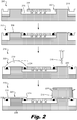
- Fig. 2 is a diagram of an example of stages of manufacturing an apparatus with low profile encapsulation according to the principles described herein.
- a first stage (200) of manufacturing involves forming gaps (202) in the polymer covering (204) that covers the die (206). Such gaps (202) are formed over the locations on the die (206) where electrical contact with the die (206) and the bonded wire (208) are desired.
- the location on the printed circuit board (210) is also prepared to receive its end of the bonded wire (208).
- the wire (208) is bonded to the die (206) and the printed circuit board (210).
- Any appropriate type of bond may be used to electrically connect the die (206) and the printed circuit board (210) to the wire (208).
- the bond may be a wedge bond, a ball bond, another type of bond, or combinations thereof.
- the bond between the bonded wire (208) and the die (206) is made in the gap (202) formed in the polymer covering (204).
- a liquid resin (216) is applied over the bonded wire (208). As the liquid resin (216) cures, the liquid resin (216) forms a solidified shape (218) as encapsulation (220).
- the solidified shape (218) is formed based on the liquid resin's surface tension, temperature, rheology characteristics, viscosity, other inherent characteristics, and combinations thereof.
- the height (224) of the encapsulation's solidified shape (218) is high enough that the encapsulation (220) may interfere with servicing the print heads. For example, the height (224) of the encapsulation (220) may interfere with wiping actions or allowing tools to access the die (206).
- the truncated shape (226) of the encapsulation is formed.
- a stamp (228) is pressed over the solidified shape (218) to form the truncated shape (226).
- the stamp (228) may include a coating (230) that prevents the encapsulation (220) from bonding with the stamp (228).
- the coating (230) may be any appropriate type of coating.
- the coating may be a plastic, a polyethylene terephthalate, polytetrafluoroethylene, another type of material, or combinations thereof.
- the stamp (228) may be heated to lower the encapsulation's viscosity while the stamp is (228) compressing the encapsulation (220). As a result, the encapsulation (220) will have a truncated shape (226).
- the truncated shape (226) may have a portion that retains the solidified shape (218) and a truncated portion (232).
- the solidified shape (218) is retained proximate the base (234) of the encapsulation (220) and the truncated portion (232) is the portion that is flat.
- the truncated shape (226) has a top-hat profile. While this example has been described with specific reference to a flat surface, in other examples, the truncated shape has a slopped, slanted, curved, or other type of surface that allows access to the die (206).
- the truncated height (235) of the encapsulation (220) from its base, such as where the encapsulation (220) contacts the compound (236), to the truncated portion (232) is less than a hundred microns. In some examples, the truncated height is between twenty five microns and a hundred microns. In such an example, the stamp (228) is brought within the appropriate distance from the compound (236).
- the stamp (228) may be brought to the truncated height (235) instantaneously or the stamp (228) may be brought to the truncated height (235) over a predetermined period of time to allow the heat from the stamp (228) to transfer to the encapsulation (220) or allow the encapsulation (220) to flow with an increasing amount of pressure exerted from the stamp (228).
- Fig. 3 is a diagram of an example of an apparatus (300) with low profile encapsulation (302) covering a bonded wire (304) according to the principles described herein.
- the liquid resin (306) is applied from an applicator (308) to the area where encapsulation (302) is desired.
- a guide (310) is positioned adjacent the region where the liquid resin (306) is applied. The guide (310) is close enough to the applied liquid resin (306) that the liquid resin (306) is attracted to the underside (312) of the guide (310) and is wicked along a length of the underside (312).
- the applicator (308) may be a needle applicator, a dropping applicator, a jetting applicator, a spray applicator, another type of applicator, or combinations thereof.
- the guide (310) is positioned to form a gap (314) between the apparatus (300) and the underside (312) of the guide (310) that is equal to the desired truncated height for the encapsulation's shape. Due to the wicking characteristics of the guide (310) and the liquid resin (306), the liquid resin (306) is drawn into and fills the gap (314).
- the gap (314) may be formed in any appropriate manner in accordance with the principles described herein.
- a spacer may be incorporated into the underside (312) of the guide (310) to ensure that the gap (314) is correct.
- Such a spacer may include a mechanism for causing the liquid resin (306) to pass around the spacer as the liquid resin (306) is applied to the desired area.
- a computer implemented mechanism may use distance sensors to determine the distance between the underside (312) of the guide (310) and the top surface of the apparatus (300).
- Such a distance sensor may use the travel of sound, the travel of optical waves, a mechanical probe, another mechanism, or combinations thereof, In some examples, the distance sensors are incorporated directly into the guide (310) or the stamp (228, Fig. 2 ).
- the guide (310) can be stationary or can be moved along the length of the bonded wire (304) along with the applicator (308) as the liquid resin fills the space underneath the guide (310). As a result, the gap (314) is progressively moved along the bonded wire's length and additional liquid resin (306) fills the new space. As a result, the liquid resin solidifies along the length of the bonded wire (304). The resulting shape is truncated as the guide (310) causes the shape to have a flat top that would not have otherwise formed without the active interaction with the guide (310).
- the guide (310 like the stamp (228, Fig. 2 ), may have a coating (316) to prevent the liquid resin (306) form attaching to the guide (310).
- the liquid resin (306) may cure in place while the guide (310) is still forming the gap (314). In some examples, the liquid resin (306) is partially cured before the guide (310) is removed. The curing process may occur as the liquid resin (306) is allowed to air cool. In other examples, the curing process is accelerated by actively cooling the liquid resin (306) into encapsulation by actively cooling the liquid resin (306).
- the encapsulation is cured in place with exposure to certain ultraviolet wavelengths.
- wavelengths of light may be guided to the encapsulation through the guide (310), the stamp (228, Fig. 2 ), another type of tool, or combinations thereof.
- the truncated shape may be formed by grinding, blading, slicing, or otherwise using another type of tool to shape the truncation.
- Fig. 4 is a diagram of an example of a method (400) for encapsulating a bonded wire with low profile encapsulation according to the principles described herein.
- the method (400) includes applying (402) encapsulation over a bonded wire that is connected to a die on a first end and to a circuit component on a second end and truncating (404) a shape of the encapsulation to form a truncated shape.
- the truncated shape is formed through a compressive mechanism.
- a stamp can be used to flatten the surface of the encapsulation or shorten the encapsulation's height.
- other devices can be used to flatten the top and reduce the encapsulation's height.
- the compressed encapsulation material may have a higher density than other encapsulation materials that are allowed to retain their shapes that are determined by the encapsulation materials surface tension and other properties.
- the compression may provide the example of removing air bubbles from the encapsulation. Further, the compression may aid in forming a stronger bond between the die, bonded wire, printed circuit board, or other surface areas of the apparatus and the encapsulation. As a result, the encapsulation may be less prone to delaminating.
- the shape is truncated by allowing the encapsulation to wick under a guide while simultaneously depositing the encapsulation and moving the guide along a length of the wire.
- the truncated shape is formed by grinding or otherwise removing a portion of the encapsulation.
- the temperature of the liquid resin used to form the encapsulation material may be controlled during the encapsulation process.
- a mechanism may be implemented to cause the liquid resin to have a high enough temperature to flow easily during application processes, compression processes, grinding processes, or other processes for forming the truncated shapes.
- the liquid resin when the liquid resin is formed in the desirable truncated shape, the liquid resin may be actively cooled to cause the encapsulation to retain the desired shape. Active cooling may occur by use of a fan, cooling the stamp or guide, or other mechanism that will cool the encapsulation.
- An advantage of the principles described herein is that the processes of stamping, guiding, blading, grinding, or otherwise forming a truncated shape is relatively inexpensive as compared to creating a low profile encapsulation through a film deposition technique. Further, the principles described herein may involve a single process for forming the truncated shape as the liquid resin is applied. In other examples, the principles described herein may involve multiple processes such as first depositing the encapsulation, allowing that encapsulation to form whatever shape is inherent to the encapsulation based on the encapsulation's inherent properties, and truncating that natural shape.
- the principles described herein allow for the encapsulation to be closer to the print heads and/or nozzles. Such an advantage allows for the electronics in printers (or the printers themselves) to be made smaller. As a result, the printers can be less expensive and more compact.
Landscapes
- Engineering & Computer Science (AREA)
- Manufacturing & Machinery (AREA)
- Computer Hardware Design (AREA)
- Microelectronics & Electronic Packaging (AREA)
- Power Engineering (AREA)
- Physics & Mathematics (AREA)
- Condensed Matter Physics & Semiconductors (AREA)
- General Physics & Mathematics (AREA)
- Encapsulation Of And Coatings For Semiconductor Or Solid State Devices (AREA)
- Particle Formation And Scattering Control In Inkjet Printers (AREA)
Applications Claiming Priority (1)
| Application Number | Priority Date | Filing Date | Title |
|---|---|---|---|
| PCT/US2013/067117 WO2015065320A1 (en) | 2013-10-28 | 2013-10-28 | Encapsulating a bonded wire with low profile encapsulation |
Publications (3)
| Publication Number | Publication Date |
|---|---|
| EP3063008A1 EP3063008A1 (en) | 2016-09-07 |
| EP3063008A4 EP3063008A4 (en) | 2017-08-16 |
| EP3063008B1 true EP3063008B1 (en) | 2020-10-07 |
Family
ID=53004742
Family Applications (1)
| Application Number | Title | Priority Date | Filing Date |
|---|---|---|---|
| EP13896622.1A Active EP3063008B1 (en) | 2013-10-28 | 2013-10-28 | Encapsulating a bonded wire with low profile encapsulation |
Country Status (5)
| Country | Link |
|---|---|
| US (2) | US20160257117A1 (zh) |
| EP (1) | EP3063008B1 (zh) |
| CN (2) | CN105705336B (zh) |
| TW (1) | TWI567835B (zh) |
| WO (1) | WO2015065320A1 (zh) |
Families Citing this family (3)
| Publication number | Priority date | Publication date | Assignee | Title |
|---|---|---|---|---|
| EP3362292B1 (en) | 2015-10-15 | 2022-03-09 | Hewlett-Packard Development Company, L.P. | Molded print head comprising an interposer and method for manufacturing a molded print head comprising an interposer |
| WO2019022735A1 (en) | 2017-07-26 | 2019-01-31 | Hewlett-Packard Development Company, L.P. | MATRIX CONTACT TRAINING |
| WO2020101659A1 (en) * | 2018-11-14 | 2020-05-22 | Hewlett-Packard Development Company, L.P. | Fluidic die assemblies with rigid bent substrates |
Citations (1)
| Publication number | Priority date | Publication date | Assignee | Title |
|---|---|---|---|---|
| EP1095773A1 (en) * | 1999-10-29 | 2001-05-02 | Hewlett-Packard Company, A Delaware Corporation | Inkjet printhead having improved reliability |
Family Cites Families (55)
| Publication number | Priority date | Publication date | Assignee | Title |
|---|---|---|---|---|
| US5018003A (en) * | 1988-10-20 | 1991-05-21 | Mitsubishi Denki Kabushiki Kaisha | Lead frame and semiconductor device |
| JPH03197147A (ja) * | 1989-12-27 | 1991-08-28 | Seiko Instr Inc | サーマルヘッドの実装構造 |
| US5367766A (en) * | 1990-08-01 | 1994-11-29 | Staktek Corporation | Ultra high density integrated circuit packages method |
| IT1247649B (it) * | 1990-10-31 | 1994-12-28 | Sgs Thomson Microelectronics | Procedimento di incapsulamento in resina di un dispositivo a semiconduttore di potenza montato su dissipatore allontanando i reofori dal dissipatore mediante l'azione del controstampo in fase di chiusura dello stampo |
| US5420752A (en) * | 1993-08-18 | 1995-05-30 | Lsi Logic Corporation | GPT system for encapsulating an integrated circuit package |
| US6359335B1 (en) * | 1994-05-19 | 2002-03-19 | Tessera, Inc. | Method of manufacturing a plurality of semiconductor packages and the resulting semiconductor package structures |
| US5682673A (en) * | 1995-04-17 | 1997-11-04 | Ipac, Inc. | Method for forming encapsulated IC packages |
| JPH09115936A (ja) * | 1995-10-23 | 1997-05-02 | Mitsubishi Electric Corp | 半導体装置の樹脂封止用金型 |
| US6071427A (en) * | 1998-06-03 | 2000-06-06 | Lexmark International, Inc. | Method for making a printhead |
| US6246111B1 (en) * | 2000-01-25 | 2001-06-12 | Siliconware Precision Industries Co., Ltd. | Universal lead frame type of quad flat non-lead package of semiconductor |
| JP4493174B2 (ja) * | 2000-07-27 | 2010-06-30 | 京セラ株式会社 | サーマルヘッド |
| US6577013B1 (en) * | 2000-09-05 | 2003-06-10 | Amkor Technology, Inc. | Chip size semiconductor packages with stacked dies |
| US6340846B1 (en) | 2000-12-06 | 2002-01-22 | Amkor Technology, Inc. | Making semiconductor packages with stacked dies and reinforced wire bonds |
| US6720207B2 (en) * | 2001-02-14 | 2004-04-13 | Matsushita Electric Industrial Co., Ltd. | Leadframe, resin-molded semiconductor device including the leadframe, method of making the leadframe and method for manufacturing the device |
| US6727115B2 (en) * | 2001-10-31 | 2004-04-27 | Hewlett-Packard Development Company, L.P. | Back-side through-hole interconnection of a die to a substrate |
| US6884663B2 (en) * | 2002-01-07 | 2005-04-26 | Delphon Industries, Llc | Method for reconstructing an integrated circuit package using lapping |
| US6743660B2 (en) * | 2002-01-12 | 2004-06-01 | Taiwan Semiconductor Manufacturing Co., Ltd | Method of making a wafer level chip scale package |
| US6653723B2 (en) | 2002-03-09 | 2003-11-25 | Fujitsu Limited | System for providing an open-cavity low profile encapsulated semiconductor package |
| US20060051948A1 (en) * | 2003-02-04 | 2006-03-09 | Microfabrica Inc. | Microprobe tips and methods for making |
| US7562428B2 (en) * | 2002-09-24 | 2009-07-21 | Brother Kogyo Kabushiki Kaisha | Manufacturing an ink jet head |
| US6987058B2 (en) * | 2003-03-18 | 2006-01-17 | Micron Technology, Inc. | Methods for underfilling and encapsulating semiconductor device assemblies with a single dielectric material |
| JP4340086B2 (ja) * | 2003-03-20 | 2009-10-07 | 株式会社日立製作所 | ナノプリント用スタンパ、及び微細構造転写方法 |
| US7527090B2 (en) * | 2003-06-30 | 2009-05-05 | Intel Corporation | Heat dissipating device with preselected designed interface for thermal interface materials |
| US7771917B2 (en) * | 2005-06-17 | 2010-08-10 | Micron Technology, Inc. | Methods of making templates for use in imprint lithography |
| KR100761387B1 (ko) * | 2005-07-13 | 2007-09-27 | 서울반도체 주식회사 | 몰딩부재를 형성하기 위한 몰드 및 그것을 사용한 몰딩부재형성방법 |
| CN2846128Y (zh) * | 2005-07-27 | 2006-12-13 | 山东华菱电子有限公司 | 热敏打印头 |
| US7691675B2 (en) * | 2005-10-24 | 2010-04-06 | Hewlett-Packard Development Company, L.P. | Encapsulating electrical connections |
| JP4939184B2 (ja) * | 2005-12-15 | 2012-05-23 | キヤノン株式会社 | 液体吐出ヘッドの製造方法 |
| US7819506B2 (en) * | 2006-03-29 | 2010-10-26 | Lexmark International, Inc. | Flexible encapsulant materials for micro-fluid ejection heads and methods relating thereto |
| US20080158298A1 (en) * | 2006-12-28 | 2008-07-03 | Serbicki Jeffrey P | Printhead wirebond encapsulation |
| CN101211897B (zh) * | 2006-12-28 | 2011-12-07 | 中芯国际集成电路制造(上海)有限公司 | 多芯片半导体封装结构及封装方法 |
| KR100843342B1 (ko) * | 2007-02-12 | 2008-07-03 | 삼성전자주식회사 | Uv 나노 임프린트 리소그래피 수행 공정 및 장치 |
| US7854877B2 (en) * | 2007-08-14 | 2010-12-21 | Asml Netherlands B.V. | Lithography meandering order |
| KR101289337B1 (ko) * | 2007-08-29 | 2013-07-29 | 시게이트 테크놀로지 엘엘씨 | 양면 임프린트 리소그래피 장치 |
| US7669751B2 (en) * | 2007-09-25 | 2010-03-02 | Silverbrook Research Pty Ltd | Method of forming low profile wire bonds between integrated circuits dies and printed circuit boards |
| WO2009039550A1 (en) * | 2007-09-25 | 2009-04-02 | Silverbrook Research Pty Ltd | Method of wire bond encapsulation profiling |
| US7741720B2 (en) * | 2007-09-25 | 2010-06-22 | Silverbrook Research Pty Ltd | Electronic device with wire bonds adhered between integrated circuits dies and printed circuit boards |
| JP2009184164A (ja) * | 2008-02-05 | 2009-08-20 | Toshiba Hokuto Electronics Corp | サーマルプリントヘッド |
| US8035211B2 (en) | 2008-03-26 | 2011-10-11 | Stats Chippac Ltd. | Integrated circuit package system with support structure under wire-in-film adhesive |
| JP5117318B2 (ja) * | 2008-08-07 | 2013-01-16 | 株式会社日立ハイテクノロジーズ | ナノインプリント用スタンパ及び該スタンパを使用する微細構造転写装置 |
| US8039938B2 (en) * | 2009-05-22 | 2011-10-18 | Palo Alto Research Center Incorporated | Airgap micro-spring interconnect with bonded underfill seal |
| CN201442383U (zh) * | 2009-07-01 | 2010-04-28 | 山东华菱电子有限公司 | 热敏打印头 |
| KR20120040536A (ko) * | 2010-10-19 | 2012-04-27 | 삼성전자주식회사 | 반도체 패키지 및 그 제조 방법 |
| CN102529416B (zh) * | 2010-11-30 | 2016-01-20 | 罗姆股份有限公司 | 热敏打印头 |
| JP5828682B2 (ja) * | 2011-06-06 | 2015-12-09 | キヤノン株式会社 | 液体吐出ヘッドの製造方法 |
| US8691341B2 (en) | 2011-09-30 | 2014-04-08 | Lexmark International, Inc. | Method of controlling the height of encapsulant on an inkjet printhead |
| US9209019B2 (en) * | 2013-09-05 | 2015-12-08 | Diftek Lasers, Inc. | Method and system for manufacturing a semi-conducting backplane |
| US8550599B2 (en) * | 2011-12-20 | 2013-10-08 | Canon Kabushiki Kaisha | Liquid ejection head and process for producing the same |
| JP6021365B2 (ja) * | 2012-03-12 | 2016-11-09 | キヤノン株式会社 | インプリント装置、それを用いた物品の製造方法 |
| JP5930832B2 (ja) * | 2012-04-27 | 2016-06-08 | キヤノン株式会社 | 光硬化物の製造方法 |
| US20140239529A1 (en) * | 2012-09-28 | 2014-08-28 | Nanonex Corporation | System and Methods For Nano-Scale Manufacturing |
| US8928134B2 (en) * | 2012-12-28 | 2015-01-06 | Taiwan Semiconductor Manufacturing Company, Ltd. | Package on package bonding structure and method for forming the same |
| WO2014115728A1 (ja) * | 2013-01-24 | 2014-07-31 | 綜研化学株式会社 | 光透過型インプリント用モールド、大面積モールドの製造方法 |
| US9859185B2 (en) * | 2016-01-28 | 2018-01-02 | Kyocera International, Inc. | Semiconductor packaging structure and package having stress release structure |
| JP7247574B2 (ja) * | 2018-12-19 | 2023-03-29 | 富士電機株式会社 | 半導体装置 |
-
2013
- 2013-10-28 CN CN201380080529.2A patent/CN105705336B/zh not_active Expired - Fee Related
- 2013-10-28 WO PCT/US2013/067117 patent/WO2015065320A1/en active Application Filing
- 2013-10-28 EP EP13896622.1A patent/EP3063008B1/en active Active
- 2013-10-28 CN CN201810244445.2A patent/CN108583018B/zh not_active Expired - Fee Related
- 2013-10-28 US US15/032,022 patent/US20160257117A1/en not_active Abandoned
-
2014
- 2014-09-11 TW TW103131388A patent/TWI567835B/zh not_active IP Right Cessation
-
2020
- 2020-01-08 US US16/737,279 patent/US10946658B2/en active Active
Patent Citations (1)
| Publication number | Priority date | Publication date | Assignee | Title |
|---|---|---|---|---|
| EP1095773A1 (en) * | 1999-10-29 | 2001-05-02 | Hewlett-Packard Company, A Delaware Corporation | Inkjet printhead having improved reliability |
Also Published As
| Publication number | Publication date |
|---|---|
| US20160257117A1 (en) | 2016-09-08 |
| TWI567835B (zh) | 2017-01-21 |
| CN108583018B (zh) | 2019-11-15 |
| EP3063008A4 (en) | 2017-08-16 |
| WO2015065320A1 (en) | 2015-05-07 |
| TW201523750A (zh) | 2015-06-16 |
| CN108583018A (zh) | 2018-09-28 |
| US10946658B2 (en) | 2021-03-16 |
| US20200139705A1 (en) | 2020-05-07 |
| CN105705336A (zh) | 2016-06-22 |
| CN105705336B (zh) | 2018-04-24 |
| EP3063008A1 (en) | 2016-09-07 |
Similar Documents
| Publication | Publication Date | Title |
|---|---|---|
| US10946658B2 (en) | Encapsulating a bonded wire with low profile encapsulation | |
| JP4695148B2 (ja) | 半導体装置及びその製造方法 | |
| JP5902102B2 (ja) | 半導体モジュールを製造するための方法およびシステム | |
| US20100224985A1 (en) | Chip-Scale Packaging with Protective Heat Spreader | |
| JP2004525357A (ja) | ウエハスケールで設けられるキャップによって保護される加速度計 | |
| JP2004523106A (ja) | 保護キャップのウエハスケール成形 | |
| US20140290059A1 (en) | Anisotropic conductive film and method of making conductive connection | |
| EP1940625B1 (en) | Encapsulating electrical connections | |
| WO2016049649A1 (en) | Packaged device with additive substrate surface modification | |
| JP2013153089A (ja) | 電子装置及びその製造方法 | |
| US20210351098A1 (en) | Packaged Semiconductor Device With Multilayer Stress Buffer | |
| US9899339B2 (en) | Discrete device mounted on substrate | |
| WO2019041366A1 (zh) | 一种线圈的制造方法、线圈、电子设备 | |
| US10836162B2 (en) | Print head interposers | |
| US20080169574A1 (en) | Direct Die Attachment | |
| JP2007281116A (ja) | 半導体装置の製造方法 | |
| CN103681455A (zh) | 管芯底部填充结构和方法 | |
| WO2016107298A1 (zh) | 一种微型模塑封装手机智能卡以及封装方法 | |
| US10504806B2 (en) | Semiconductor package with electrical test pads | |
| KR101366919B1 (ko) | Sr 포스트 형성방법 및 이를 이용한 전자소자 패키지 제조방법 | |
| KR100790461B1 (ko) | 전자 패키지 제조방법 | |
| TW200915524A (en) | Integrated circuit support for low profile wire bond | |
| CA2957999A1 (en) | Method to provide die attach stress relief using gold stud bumps |
Legal Events
| Date | Code | Title | Description |
|---|---|---|---|
| PUAI | Public reference made under article 153(3) epc to a published international application that has entered the european phase |
Free format text: ORIGINAL CODE: 0009012 |
|
| 17P | Request for examination filed |
Effective date: 20160329 |
|
| AK | Designated contracting states |
Kind code of ref document: A1 Designated state(s): AL AT BE BG CH CY CZ DE DK EE ES FI FR GB GR HR HU IE IS IT LI LT LU LV MC MK MT NL NO PL PT RO RS SE SI SK SM TR |
|
| AX | Request for extension of the european patent |
Extension state: BA ME |
|
| DAX | Request for extension of the european patent (deleted) | ||
| A4 | Supplementary search report drawn up and despatched |
Effective date: 20170718 |
|
| RIC1 | Information provided on ipc code assigned before grant |
Ipc: B41J 2/045 20060101AFI20170712BHEP Ipc: B41J 2/05 20060101ALI20170712BHEP |
|
| RAP1 | Party data changed (applicant data changed or rights of an application transferred) |
Owner name: HEWLETT-PACKARD DEVELOPMENT COMPANY, L.P. |
|
| STAA | Information on the status of an ep patent application or granted ep patent |
Free format text: STATUS: EXAMINATION IS IN PROGRESS |
|
| 17Q | First examination report despatched |
Effective date: 20191111 |
|
| GRAP | Despatch of communication of intention to grant a patent |
Free format text: ORIGINAL CODE: EPIDOSNIGR1 |
|
| STAA | Information on the status of an ep patent application or granted ep patent |
Free format text: STATUS: GRANT OF PATENT IS INTENDED |
|
| INTG | Intention to grant announced |
Effective date: 20200617 |
|
| GRAS | Grant fee paid |
Free format text: ORIGINAL CODE: EPIDOSNIGR3 |
|
| GRAA | (expected) grant |
Free format text: ORIGINAL CODE: 0009210 |
|
| STAA | Information on the status of an ep patent application or granted ep patent |
Free format text: STATUS: THE PATENT HAS BEEN GRANTED |
|
| AK | Designated contracting states |
Kind code of ref document: B1 Designated state(s): AL AT BE BG CH CY CZ DE DK EE ES FI FR GB GR HR HU IE IS IT LI LT LU LV MC MK MT NL NO PL PT RO RS SE SI SK SM TR |
|
| REG | Reference to a national code |
Ref country code: GB Ref legal event code: FG4D |
|
| REG | Reference to a national code |
Ref country code: CH Ref legal event code: EP Ref country code: AT Ref legal event code: REF Ref document number: 1320735 Country of ref document: AT Kind code of ref document: T Effective date: 20201015 |
|
| REG | Reference to a national code |
Ref country code: IE Ref legal event code: FG4D |
|
| REG | Reference to a national code |
Ref country code: DE Ref legal event code: R096 Ref document number: 602013073196 Country of ref document: DE |
|
| REG | Reference to a national code |
Ref country code: NL Ref legal event code: MP Effective date: 20201007 |
|
| REG | Reference to a national code |
Ref country code: AT Ref legal event code: MK05 Ref document number: 1320735 Country of ref document: AT Kind code of ref document: T Effective date: 20201007 |
|
| PG25 | Lapsed in a contracting state [announced via postgrant information from national office to epo] |
Ref country code: RS Free format text: LAPSE BECAUSE OF FAILURE TO SUBMIT A TRANSLATION OF THE DESCRIPTION OR TO PAY THE FEE WITHIN THE PRESCRIBED TIME-LIMIT Effective date: 20201007 Ref country code: FI Free format text: LAPSE BECAUSE OF FAILURE TO SUBMIT A TRANSLATION OF THE DESCRIPTION OR TO PAY THE FEE WITHIN THE PRESCRIBED TIME-LIMIT Effective date: 20201007 Ref country code: PT Free format text: LAPSE BECAUSE OF FAILURE TO SUBMIT A TRANSLATION OF THE DESCRIPTION OR TO PAY THE FEE WITHIN THE PRESCRIBED TIME-LIMIT Effective date: 20210208 Ref country code: NO Free format text: LAPSE BECAUSE OF FAILURE TO SUBMIT A TRANSLATION OF THE DESCRIPTION OR TO PAY THE FEE WITHIN THE PRESCRIBED TIME-LIMIT Effective date: 20210107 Ref country code: NL Free format text: LAPSE BECAUSE OF FAILURE TO SUBMIT A TRANSLATION OF THE DESCRIPTION OR TO PAY THE FEE WITHIN THE PRESCRIBED TIME-LIMIT Effective date: 20201007 Ref country code: GR Free format text: LAPSE BECAUSE OF FAILURE TO SUBMIT A TRANSLATION OF THE DESCRIPTION OR TO PAY THE FEE WITHIN THE PRESCRIBED TIME-LIMIT Effective date: 20210108 |
|
| REG | Reference to a national code |
Ref country code: LT Ref legal event code: MG4D |
|
| PG25 | Lapsed in a contracting state [announced via postgrant information from national office to epo] |
Ref country code: AT Free format text: LAPSE BECAUSE OF FAILURE TO SUBMIT A TRANSLATION OF THE DESCRIPTION OR TO PAY THE FEE WITHIN THE PRESCRIBED TIME-LIMIT Effective date: 20201007 Ref country code: ES Free format text: LAPSE BECAUSE OF FAILURE TO SUBMIT A TRANSLATION OF THE DESCRIPTION OR TO PAY THE FEE WITHIN THE PRESCRIBED TIME-LIMIT Effective date: 20201007 Ref country code: BG Free format text: LAPSE BECAUSE OF FAILURE TO SUBMIT A TRANSLATION OF THE DESCRIPTION OR TO PAY THE FEE WITHIN THE PRESCRIBED TIME-LIMIT Effective date: 20210107 Ref country code: SE Free format text: LAPSE BECAUSE OF FAILURE TO SUBMIT A TRANSLATION OF THE DESCRIPTION OR TO PAY THE FEE WITHIN THE PRESCRIBED TIME-LIMIT Effective date: 20201007 Ref country code: PL Free format text: LAPSE BECAUSE OF FAILURE TO SUBMIT A TRANSLATION OF THE DESCRIPTION OR TO PAY THE FEE WITHIN THE PRESCRIBED TIME-LIMIT Effective date: 20201007 Ref country code: IS Free format text: LAPSE BECAUSE OF FAILURE TO SUBMIT A TRANSLATION OF THE DESCRIPTION OR TO PAY THE FEE WITHIN THE PRESCRIBED TIME-LIMIT Effective date: 20210207 Ref country code: LV Free format text: LAPSE BECAUSE OF FAILURE TO SUBMIT A TRANSLATION OF THE DESCRIPTION OR TO PAY THE FEE WITHIN THE PRESCRIBED TIME-LIMIT Effective date: 20201007 |
|
| REG | Reference to a national code |
Ref country code: CH Ref legal event code: PL |
|
| PG25 | Lapsed in a contracting state [announced via postgrant information from national office to epo] |
Ref country code: LU Free format text: LAPSE BECAUSE OF NON-PAYMENT OF DUE FEES Effective date: 20201028 Ref country code: HR Free format text: LAPSE BECAUSE OF FAILURE TO SUBMIT A TRANSLATION OF THE DESCRIPTION OR TO PAY THE FEE WITHIN THE PRESCRIBED TIME-LIMIT Effective date: 20201007 |
|
| REG | Reference to a national code |
Ref country code: DE Ref legal event code: R097 Ref document number: 602013073196 Country of ref document: DE |
|
| REG | Reference to a national code |
Ref country code: BE Ref legal event code: MM Effective date: 20201031 |
|
| PG25 | Lapsed in a contracting state [announced via postgrant information from national office to epo] |
Ref country code: MC Free format text: LAPSE BECAUSE OF FAILURE TO SUBMIT A TRANSLATION OF THE DESCRIPTION OR TO PAY THE FEE WITHIN THE PRESCRIBED TIME-LIMIT Effective date: 20201007 Ref country code: LT Free format text: LAPSE BECAUSE OF FAILURE TO SUBMIT A TRANSLATION OF THE DESCRIPTION OR TO PAY THE FEE WITHIN THE PRESCRIBED TIME-LIMIT Effective date: 20201007 Ref country code: RO Free format text: LAPSE BECAUSE OF FAILURE TO SUBMIT A TRANSLATION OF THE DESCRIPTION OR TO PAY THE FEE WITHIN THE PRESCRIBED TIME-LIMIT Effective date: 20201007 Ref country code: SK Free format text: LAPSE BECAUSE OF FAILURE TO SUBMIT A TRANSLATION OF THE DESCRIPTION OR TO PAY THE FEE WITHIN THE PRESCRIBED TIME-LIMIT Effective date: 20201007 Ref country code: CZ Free format text: LAPSE BECAUSE OF FAILURE TO SUBMIT A TRANSLATION OF THE DESCRIPTION OR TO PAY THE FEE WITHIN THE PRESCRIBED TIME-LIMIT Effective date: 20201007 Ref country code: EE Free format text: LAPSE BECAUSE OF FAILURE TO SUBMIT A TRANSLATION OF THE DESCRIPTION OR TO PAY THE FEE WITHIN THE PRESCRIBED TIME-LIMIT Effective date: 20201007 Ref country code: SM Free format text: LAPSE BECAUSE OF FAILURE TO SUBMIT A TRANSLATION OF THE DESCRIPTION OR TO PAY THE FEE WITHIN THE PRESCRIBED TIME-LIMIT Effective date: 20201007 |
|
| PLBE | No opposition filed within time limit |
Free format text: ORIGINAL CODE: 0009261 |
|
| STAA | Information on the status of an ep patent application or granted ep patent |
Free format text: STATUS: NO OPPOSITION FILED WITHIN TIME LIMIT |
|
| PG25 | Lapsed in a contracting state [announced via postgrant information from national office to epo] |
Ref country code: DK Free format text: LAPSE BECAUSE OF FAILURE TO SUBMIT A TRANSLATION OF THE DESCRIPTION OR TO PAY THE FEE WITHIN THE PRESCRIBED TIME-LIMIT Effective date: 20201007 Ref country code: CH Free format text: LAPSE BECAUSE OF NON-PAYMENT OF DUE FEES Effective date: 20201031 Ref country code: BE Free format text: LAPSE BECAUSE OF NON-PAYMENT OF DUE FEES Effective date: 20201031 Ref country code: LI Free format text: LAPSE BECAUSE OF NON-PAYMENT OF DUE FEES Effective date: 20201031 |
|
| 26N | No opposition filed |
Effective date: 20210708 |
|
| PG25 | Lapsed in a contracting state [announced via postgrant information from national office to epo] |
Ref country code: AL Free format text: LAPSE BECAUSE OF FAILURE TO SUBMIT A TRANSLATION OF THE DESCRIPTION OR TO PAY THE FEE WITHIN THE PRESCRIBED TIME-LIMIT Effective date: 20201007 Ref country code: IT Free format text: LAPSE BECAUSE OF FAILURE TO SUBMIT A TRANSLATION OF THE DESCRIPTION OR TO PAY THE FEE WITHIN THE PRESCRIBED TIME-LIMIT Effective date: 20201007 Ref country code: IE Free format text: LAPSE BECAUSE OF NON-PAYMENT OF DUE FEES Effective date: 20201028 |
|
| PGFP | Annual fee paid to national office [announced via postgrant information from national office to epo] |
Ref country code: FR Payment date: 20210921 Year of fee payment: 9 |
|
| PG25 | Lapsed in a contracting state [announced via postgrant information from national office to epo] |
Ref country code: SI Free format text: LAPSE BECAUSE OF FAILURE TO SUBMIT A TRANSLATION OF THE DESCRIPTION OR TO PAY THE FEE WITHIN THE PRESCRIBED TIME-LIMIT Effective date: 20201007 |
|
| PGFP | Annual fee paid to national office [announced via postgrant information from national office to epo] |
Ref country code: GB Payment date: 20210922 Year of fee payment: 9 |
|
| PGFP | Annual fee paid to national office [announced via postgrant information from national office to epo] |
Ref country code: DE Payment date: 20210921 Year of fee payment: 9 |
|
| PG25 | Lapsed in a contracting state [announced via postgrant information from national office to epo] |
Ref country code: IS Free format text: LAPSE BECAUSE OF FAILURE TO SUBMIT A TRANSLATION OF THE DESCRIPTION OR TO PAY THE FEE WITHIN THE PRESCRIBED TIME-LIMIT Effective date: 20210207 Ref country code: TR Free format text: LAPSE BECAUSE OF FAILURE TO SUBMIT A TRANSLATION OF THE DESCRIPTION OR TO PAY THE FEE WITHIN THE PRESCRIBED TIME-LIMIT Effective date: 20201007 Ref country code: MT Free format text: LAPSE BECAUSE OF FAILURE TO SUBMIT A TRANSLATION OF THE DESCRIPTION OR TO PAY THE FEE WITHIN THE PRESCRIBED TIME-LIMIT Effective date: 20201007 Ref country code: CY Free format text: LAPSE BECAUSE OF FAILURE TO SUBMIT A TRANSLATION OF THE DESCRIPTION OR TO PAY THE FEE WITHIN THE PRESCRIBED TIME-LIMIT Effective date: 20201007 |
|
| PG25 | Lapsed in a contracting state [announced via postgrant information from national office to epo] |
Ref country code: MK Free format text: LAPSE BECAUSE OF FAILURE TO SUBMIT A TRANSLATION OF THE DESCRIPTION OR TO PAY THE FEE WITHIN THE PRESCRIBED TIME-LIMIT Effective date: 20201007 |
|
| REG | Reference to a national code |
Ref country code: DE Ref legal event code: R119 Ref document number: 602013073196 Country of ref document: DE |
|
| GBPC | Gb: european patent ceased through non-payment of renewal fee |
Effective date: 20221028 |
|
| PG25 | Lapsed in a contracting state [announced via postgrant information from national office to epo] |
Ref country code: FR Free format text: LAPSE BECAUSE OF NON-PAYMENT OF DUE FEES Effective date: 20221031 Ref country code: DE Free format text: LAPSE BECAUSE OF NON-PAYMENT OF DUE FEES Effective date: 20230503 |
|
| PG25 | Lapsed in a contracting state [announced via postgrant information from national office to epo] |
Ref country code: GB Free format text: LAPSE BECAUSE OF NON-PAYMENT OF DUE FEES Effective date: 20221028 |