EP3025378B1 - Method of separating light emitting devices formed on a substrate wafer - Google Patents
Method of separating light emitting devices formed on a substrate wafer Download PDFInfo
- Publication number
- EP3025378B1 EP3025378B1 EP14752405.2A EP14752405A EP3025378B1 EP 3025378 B1 EP3025378 B1 EP 3025378B1 EP 14752405 A EP14752405 A EP 14752405A EP 3025378 B1 EP3025378 B1 EP 3025378B1
- Authority
- EP
- European Patent Office
- Prior art keywords
- substrate
- leds
- sapphire substrate
- light emitting
- cracks
- Prior art date
- Legal status (The legal status is an assumption and is not a legal conclusion. Google has not performed a legal analysis and makes no representation as to the accuracy of the status listed.)
- Active
Links
Images

Classifications
-
- H—ELECTRICITY
- H10—SEMICONDUCTOR DEVICES; ELECTRIC SOLID-STATE DEVICES NOT OTHERWISE PROVIDED FOR
- H10H—INORGANIC LIGHT-EMITTING SEMICONDUCTOR DEVICES HAVING POTENTIAL BARRIERS
- H10H20/00—Individual inorganic light-emitting semiconductor devices having potential barriers, e.g. light-emitting diodes [LED]
- H10H20/01—Manufacture or treatment
- H10H20/011—Manufacture or treatment of bodies, e.g. forming semiconductor layers
- H10H20/013—Manufacture or treatment of bodies, e.g. forming semiconductor layers having light-emitting regions comprising only Group III-V materials
- H10H20/0133—Manufacture or treatment of bodies, e.g. forming semiconductor layers having light-emitting regions comprising only Group III-V materials with a substrate not being Group III-V materials
- H10H20/01335—Manufacture or treatment of bodies, e.g. forming semiconductor layers having light-emitting regions comprising only Group III-V materials with a substrate not being Group III-V materials the light-emitting regions comprising nitride materials
-
- H—ELECTRICITY
- H10—SEMICONDUCTOR DEVICES; ELECTRIC SOLID-STATE DEVICES NOT OTHERWISE PROVIDED FOR
- H10H—INORGANIC LIGHT-EMITTING SEMICONDUCTOR DEVICES HAVING POTENTIAL BARRIERS
- H10H20/00—Individual inorganic light-emitting semiconductor devices having potential barriers, e.g. light-emitting diodes [LED]
- H10H20/01—Manufacture or treatment
- H10H20/011—Manufacture or treatment of bodies, e.g. forming semiconductor layers
- H10H20/018—Bonding of wafers
-
- H—ELECTRICITY
- H10—SEMICONDUCTOR DEVICES; ELECTRIC SOLID-STATE DEVICES NOT OTHERWISE PROVIDED FOR
- H10H—INORGANIC LIGHT-EMITTING SEMICONDUCTOR DEVICES HAVING POTENTIAL BARRIERS
- H10H20/00—Individual inorganic light-emitting semiconductor devices having potential barriers, e.g. light-emitting diodes [LED]
- H10H20/80—Constructional details
- H10H20/81—Bodies
- H10H20/819—Bodies characterised by their shape, e.g. curved or truncated substrates
-
- H—ELECTRICITY
- H10—SEMICONDUCTOR DEVICES; ELECTRIC SOLID-STATE DEVICES NOT OTHERWISE PROVIDED FOR
- H10P—GENERIC PROCESSES OR APPARATUS FOR THE MANUFACTURE OR TREATMENT OF DEVICES COVERED BY CLASS H10
- H10P54/00—Cutting or separating of wafers, substrates or parts of devices
Definitions
- the present invention relates to methods for separating light emitting devices grown on a substrate wafer.
- LEDs light emitting diodes
- RCLEDs resonant cavity light emitting diodes
- VCSELs vertical cavity laser diodes
- edge emitting lasers are among the most efficient light sources currently available.
- Materials systems currently of interest in the manufacture of high-brightness light emitting devices capable of operation across the visible spectrum include Group III-V semiconductors, particularly binary, ternary, and quaternary alloys of gallium, aluminum, indium, and nitrogen, also referred to as III-nitride materials.
- III-nitride light emitting devices are fabricated by epitaxially growing a stack of semiconductor layers of different compositions and dopant concentrations on a sapphire, silicon carbide, III-nitride, or other suitable substrate by metal-organic chemical vapor deposition (MOCVD), molecular beam epitaxy (MBE), or other epitaxial techniques.
- MOCVD metal-organic chemical vapor deposition
- MBE molecular beam epitaxy
- the stack often includes one or more n-type layers doped with, for example, Si, formed over the substrate, one or more light emitting layers in an active region formed over the n-type layer or layers, and one or more p-type layers doped with, for example, Mg, formed over the active region. Electrical contacts are formed on the n- and p-type regions.
- the growth substrate remains part of the final device structure, for example to provide mechanical stability to the semiconductor structure.
- a significant amount of light may be emitted through the sides of the growth substrate. Side light emission from the substrate is undesirable in applications that require or prefer that most or all of the light be emitted from the top of the device.
- US 2010/0267219 describes a method of thinning the growth substrate. According to the abstract, the method includes "a sapphire substrate grinding step of grinding the back side of the sapphire substrate; a modified layer forming step of applying a laser beam to the sapphire substrate from the back side thereof to thereby form a modified layer in the sapphire substrate along each street; ... and a wafer dividing step of breaking the sapphire substrate along each street where the modified layer is formed".
- US 2013/029445 A1 discloses a method of manufacturing a semiconductor light emitting device including: preparing a substrate having a first and a second main surfaces opposing each other; forming a plurality of protruding parts in the first main surface of the substrate; forming a light emitting stack on the first main surface on which the plurality of protruding parts are formed; forming a plurality of light emitting structures by removing portions of the light emitting stack formed in regions corresponding to groove parts around the plurality of protruding parts; and separating the substrate along the groove parts.
- EP 1 376 687 A2 A discloses a method wherein a plurality of Group III nitride compound semiconductor layers are formed on a substrate for performing the formation of elements and the formation of electrodes.
- the Group III nitride compound semiconductor layers on parting lines are removed by etching or dicing due to a dicer so that only an electrode-forming layer on a side near the substrate remains or no Group III nitride compound semiconductor layer remains on the parting lines.
- a protective film is formed on the whole front surface. Separation grooves are formed in the front surface of the substrate by laser beam irradiation. The protective film is removed together with reaction products produced by the laser beam irradiation.
- the rear surface of the substrate is polished to reduce the thickness of the substrate. Then, rear grooves corresponding to the latticed frame-shaped parting lines are formed in the rear surface of the substrate.
- the substrate is divided into individual elements along the parting lines.
- WO 2005/122223 A1 discloses a method for producing a compound semiconductor device wafer, which method enables cleaving of a wafer.
- the wafer includes a substrate and a plurality of compound semiconductor devices provided on the substrate and arranged with separation zones being disposed between the compound semiconductor devices, comprises a step of forming separation grooves, through laser processing, on the top surface of the substrate at the separation zones under the condition that a compound semiconductor layer is present on the top surface of the substrate.
- US 2011/198665 A1 discloses a semiconductor device and a method to provide such semiconductor device.
- the method including wet etching of dicing streets.
- the method according to the invention includes growing on a first surface of a sapphire substrate a semiconductor structure including a light emitting layer disposed between an n-type region and a p-type region.
- the semiconductor structure is formed into a plurality of LEDs.
- the sapphire substrate is thinned from a second surface of the sapphire substrate in a first thinning process.
- the second surface of the sapphire substrate is opposite the first surface of the sapphire substrate.
- cracks are formed in the sapphire substrate. The cracks extend from the first surface of the sapphire substrate and do not penetrate an entire thickness of the sapphire substrate.
- the sapphire substrate is thinned from the second surface of the sapphire substrate in a second thinning process.
- a sapphire growth substrate remains part of the final device structure, but is thinned to reduce or eliminate light emission from the sides of the growth substrate.
- Other growth substrates may be used, which do not form part of the claimed invention.
- the wafer is first partially separated by forming separation zones, which are often notches or cracks in the substrate, through at least part of the thickness of the substrate. The wafer is then fully separated by thinning the substrate until the separation zones are reached.
- separation zones which are often notches or cracks in the substrate, through at least part of the thickness of the substrate.
- the wafer is then fully separated by thinning the substrate until the separation zones are reached.
- Embodiments of the invention are particularly suited to applications that require all or a significant portion of light to be emitted from the top surface of a device, such as some automotive applications.
- semiconductor light emitting devices are III-nitride LEDs that emit blue or UV light
- semiconductor light emitting devices besides LEDs such as laser diodes and semiconductor light emitting devices made from other materials systems such as other III-V materials, III-phosphide, III-arsenide, II-VI materials, ZnO, or Si-based materials may be used.
- Fig. 1 illustrates a single III-nitride LED 12 that may be used in embodiments of the present invention. Any suitable semiconductor light emitting device may be used and embodiments of the invention are not limited to the device illustrated in Fig. 1 .
- the device of Fig. 1 is formed by growing a III-nitride semiconductor structure on a portion of a growth substrate 10 as is known in the art.
- the growth substrate is sapphire but in embodiments not forming part of the claimed invention may be any suitable substrate such as, for example, SiC, Si, GaN, or a composite substrate.
- the semiconductor structure includes a light emitting or active region sandwiched between n- and p-type regions.
- An n-type region 14 may be grown first and may include multiple layers of different compositions and dopant concentration including, for example, preparation layers such as buffer layers or nucleation layers, and/or layers designed to facilitate removal of the growth substrate, which may be n-type or not intentionally doped, and n- or even p-type device layers designed for particular optical, material, or electrical properties desirable for the light emitting region to efficiently emit light.
- a light emitting or active region 16 is grown over the n-type region 14. Examples of suitable light emitting regions include a single thick or thin light emitting layer, or a multiple quantum well light emitting region including multiple thin or thick light emitting layers separated by barrier layers.
- a p-type region 18 may then be grown over the light emitting region 16. Like the n-type region 14, the p-type region 18 may include multiple layers of different composition, thickness, and dopant concentration, including layers that are not intentionally doped, or n-type layers.
- a p-contact 20 is formed on the surface of the p-type region.
- the p-contact 20 often includes multiple conductive layers such as a reflective metal and a guard metal which may prevent or reduce electromigration of the reflective metal.
- the reflective metal is often silver but any suitable material or materials may be used.
- a portion of the p-contact 20, the p-type region 18, and the active region 16 is removed to expose a portion of the n-type region 14 on which an n-contact 22 is formed.
- the n- and p-contacts 22 and 20 are electrically isolated from each other by a gap 25, shown hatched, which may be filled with a dielectric such as an oxide of silicon or any other suitable material.
- n-contact vias may be formed; the n- and p-contacts 22 and 20 are not limited to the arrangement illustrated in Fig. 1 .
- the n- and p-contacts may be redistributed to form bond pads with a dielectric/metal stack, as is known in the art.
- one or more interconnects 26 and 28 are formed on or electrically connected to the n- and p-contacts 22 and 20.
- Interconnect 26 is electrically connected to n-contact 22 in Fig. 1 .
- Interconnect 28 is electrically connected to p-contact 20.
- Interconnects 26 and 28 are electrically isolated from the n- and p-contacts 22 and 20 and from each other by dielectric layer 24, shown hatched, and gap 27.
- Interconnects 26 and 28 may be, for example, solder, stud bumps, gold layers, or any other suitable structure.
- Many individual LEDs 12 may be formed on a single wafer then diced from a wafer of devices, as described below.
- the techniques described may be used to separate a wafer into groups of LEDs.
- the embodiments below refer to a sapphire growth substrate, the techniques described may be applied to any suitable substrate, which falls outside the scope of the claimed invention.
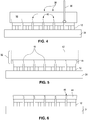
- FIG. 2-6 One embodiment of the invention is illustrated in Figs. 2, 3 , 4, 5, and 6 .
- the substrate 10 is thinned, then scribed, then thinned again.
- LEDs 12 may be the devices illustrated in Fig. 1 or any other suitable device. Although six LEDs 12 are shown, there is no expressed limit to the number of LEDs that may be created on a single substrate, nor are these LEDS required to be in a group. The LEDs in the figure are simply examples of a "some" LEDs on a portion of a substrate 10 or a complete substrate 10.
- wafer handling tape 34 is attached to LEDs 12.
- a portion 30 of the thickness of the growth substrate 10 is removed by any suitable technique such as, for example, mechanical techniques such as grinding leaving a remaining portion 32.
- the substrate 10 is thinned to a thickness which accommodates the scribing described in Fig. 4 .
- the thickness of the substrate 10 in Fig. 2 before thinning may be, for example, at least 300 ⁇ m thick in some embodiments and no more than 1500 ⁇ m thick in some embodiments, though the substrate may be thicker than 1500 ⁇ m in some embodiments.
- the remaining portion 32 of substrate 10 may be, for example, no more than 300 ⁇ m thick in some embodiments, no more than 275 ⁇ m thick in some embodiments, and no more than 250 ⁇ m thick in some embodiments.
- Fig. 4 the regions 38 between individual LEDs 12 or groups of LEDs 12 are scribed to form cracks or notches 40 in the remaining portion of substrate 32.
- the cracks 40 are localized in a portion of the thickness of the substrate 32 that is closest to LEDs 12.
- the cracks 40 do not fully penetrate the remaining portion of substrate 32.
- Cracks 40 may be formed by, for example, laser scribing, where a laser 36 is shined through the substrate 32 in regions 38, or stealth dicing, where a modified layer in the substrate is formed by focusing a laser inside the substrate.
- a femto-second laser with wavelengths between 266 and 355 nm may be used for laser scribing and a laser with wavelengths between 800 and 1100 nm may be used for stealth dicing.
- the remaining portion 32 of the sapphire substrate 10 is then thinned to expose the tops of cracks 40 formed in Fig. 4 .
- the substrate may be thinned by any suitable technique including mechanical techniques such as grinding.
- the thickness of the removed portion 42 of remaining portion 32 may be at least 100 ⁇ m thick in some embodiments and no more than 200 ⁇ m thick in some embodiments.
- the cracked portion 44 remaining after thinning may be, for example, no more than 60 ⁇ m thick in some embodiments, no more than 50 ⁇ m thick in some embodiments, and no more than 40 ⁇ m thick in some embodiments.
- the cracked portion 44 remaining after thinning is sufficiently thick in some embodiments to mechanically support the semiconductor structure.
- some or all of the cracks 40 extend through the entire remaining thickness of cracked portion 44.
- Preferably all of the cracks 40 extend through the entire remaining thickness of cracked portion 44.
- tape 34 may be stretched to separate individual LEDs 12 or groups of LEDs 12 in the gaps 46 where cracks 40 were formed.
- Each LED 12 or group of LEDs 12 has a small piece of substrate 10 (cracked portion 44) attached to the top of the semiconductor structure.
- the cracked portion 44 may be thick enough to mechanically support the semiconductor structure.
- the cracked portions 44 may have smooth or rough edges.
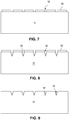
- FIG. 7-11 A reference embodiment, not being part of the invention, is illustrated in Figs. 7, 8, 9 , 10, and 11 .
- the substrate is etched, then thinned.
- a mask 50 is formed over a sapphire substrate 10 and patterned to form openings 52 aligned with areas where the substrate is later separated.
- the openings 52 may correspond to the edges of a single LED or multiple LEDs in a group.
- the semiconductor structure may be grown on substrate 10 before or after forming openings 52.
- the semiconductor structure may be patterned such that the semiconductor structure is removed from regions between LEDs.
- the sapphire substrate 10 is etched to form notches 54 in substrate 10 in the openings 52 in mask 50.
- notches 54 are at least one micron deep.
- notches 54 are at least one micron wide.
- the substrate 10 is etched by any suitable technique such as, for example, dry etching or wet etching.
- Fig. 9 the mask 50 is stripped, leaving substrate 10 with notches 54 formed in regions 52.
- notches are formed in the substrate 10 by a technique other than etching.
- notches 54 may be formed by laser scribing or stealth dicing, as described above, by laser dicing with a UV laser with a wavelength between 266 and 355 nm, or by mechanical dicing, for example using a blade. Such techniques may not require first masking the substrate, though a patterned mask may be used.
- LEDs 12 are formed in the regions between notches 54.
- the semiconductor structures grown on substrate 10 may be formed into LEDs by etching and forming metal layers to form contacts and interconnects, as described above in reference to Fig. 1 .
- the LEDs 12 are connected to wafer handling tape 34.
- Substrate 10 is thinned by any suitable technique, as described above.
- the portion 56 of the substrate 10 that is removed is sufficiently thick that some or all of notches 54 are exposed, separating individual LEDs 12 or groups of LEDs. Preferably all notches 54 are exposed.
- a portion 50 of substrate 10 remains attached to each LED 12 or group of LEDs. Portion 50 is sufficiently thick in some embodiments to mechanically support the semiconductor structure of LEDs 12.
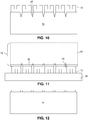
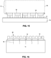
- FIG. 12 A reference embodiment, not being part of the invention, is illustrated in Figs. 12 , 13 , 14 , and 15 .
- the LEDs are partially formed, the substrate is notched, the LEDs are completed, then the substrate is thinned.
- LEDs are partially formed on substrate 10.
- the semiconductor structure of the LEDs may be grown on substrate 10.
- notches 54 are formed in the substrate 10 in the regions 52 between individual LEDs or between groups of LEDs. Notches 54 may be formed by any suitable technique, including, for example, etching, sawing, or laser scribing.
- the LEDs 12 are completed for example by etching and forming metal layers to form contacts and interconnects, as described above in reference to Fig. 1 .
- the LEDs 12 are connected to wafer handling tape 34.
- Substrate 10 is thinned by any suitable technique, as described above.
- the portion 56 of the substrate 10 that is removed is sufficiently thick that some or all of notches 54 are exposed, separating individual LEDs 12 or groups of LEDs. Preferably all notches 54 are exposed.
- a portion 50 of substrate 10 remains attached to each LED 12 or group of LEDs. Portion 50 is sufficiently thick in some embodiments to mechanically support the semiconductor structure of LEDs 12.
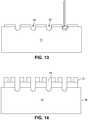
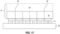
- LEDs 12 are grown on a substrate 10.
- LEDs 12 may be the devices illustrated in Fig. 1 or any other suitable device.
- Regions 38 between individual LEDs 12 or groups of LEDs 12 are laser scribed from the side of the substrate 10 on which LEDs 12 are formed.
- the scribing forms cracks or notches 40 in a portion of the thickness of substrate 10.
- the cracks 40 are localized in a portion of the thickness of the substrate that is closest to LEDs 12. Cracks 40 may be, for example, at least 30 ⁇ m deep in some embodiments, and no more than 100 ⁇ m in some embodiments.
- LEDs 12 is then mounted on a structure 34 such as a frame, support wafer, or handling tape, as shown in Fig. 17 .
- a portion 30 of the thickness of the growth substrate 10 is removed by any suitable technique such as, for example, mechanical techniques such as grinding.
- the thickness of the substrate 10 before thinning may be, for example, between 300 and 2000 ⁇ m.
- the substrate is thinned beyond a thickness where some or all of the tops of cracks 40 (in the orientation illustrated in Fig. 17 ) are reached. Preferably all of the tops of cracks 40 are reached.
- the remaining portion 32 of substrate 10 is sufficiently thick to mechanically support the semiconductor structure of LEDs 12 in some embodiments.
- Light emitting devices formed by the techniques described above may have several advantages. Because some of the substrate remains attached to the final device, the fragile semiconductor structure is supported by the substrate, which may reduce the occurrence of failure due to cracking, may eliminate the need for expensive and complex thick metal interconnects that support the semiconductor structure, and may eliminate the need for underfill or other structures to support the semiconductor structure.
- the device can be solder mounted.
- the substrate is thinned, the amount of light that escapes through the sides of the substrate may be reduced as compared to a device where the entire thickness of the substrate remains attached to the semiconductor structure. Accordingly, devices formed by the techniques described above may avoid or reduce an efficiency penalty typically associated with devices where the substrate remains attached to the semiconductor structure.
Landscapes
- Led Devices (AREA)
- Laser Beam Processing (AREA)
- Dicing (AREA)
- Drying Of Semiconductors (AREA)
Applications Claiming Priority (2)
| Application Number | Priority Date | Filing Date | Title |
|---|---|---|---|
| US201361856857P | 2013-07-22 | 2013-07-22 | |
| PCT/IB2014/062784 WO2015011583A1 (en) | 2013-07-22 | 2014-07-02 | Method of separating light emitting devices formed on a substrate wafer |
Publications (2)
| Publication Number | Publication Date |
|---|---|
| EP3025378A1 EP3025378A1 (en) | 2016-06-01 |
| EP3025378B1 true EP3025378B1 (en) | 2020-05-06 |
Family
ID=51355579
Family Applications (1)
| Application Number | Title | Priority Date | Filing Date |
|---|---|---|---|
| EP14752405.2A Active EP3025378B1 (en) | 2013-07-22 | 2014-07-02 | Method of separating light emitting devices formed on a substrate wafer |
Country Status (7)
| Country | Link |
|---|---|
| US (3) | US10079327B2 (enExample) |
| EP (1) | EP3025378B1 (enExample) |
| JP (2) | JP6429872B2 (enExample) |
| KR (1) | KR102231083B1 (enExample) |
| CN (1) | CN105556684B (enExample) |
| TW (2) | TWI726494B (enExample) |
| WO (1) | WO2015011583A1 (enExample) |
Families Citing this family (23)
| Publication number | Priority date | Publication date | Assignee | Title |
|---|---|---|---|---|
| US11792898B2 (en) | 2012-07-01 | 2023-10-17 | Ideal Industries Lighting Llc | Enhanced fixtures for area lighting |
| US11160148B2 (en) | 2017-06-13 | 2021-10-26 | Ideal Industries Lighting Llc | Adaptive area lamp |
| DE102015109413A1 (de) * | 2015-06-12 | 2016-12-15 | Osram Opto Semiconductors Gmbh | Verfahren zur Herstellung von optoelektronischen Konversions-Halbleiterchips und Verbund von Konversions-Halbleiterchips |
| US10529696B2 (en) | 2016-04-12 | 2020-01-07 | Cree, Inc. | High density pixelated LED and devices and methods thereof |
| US10818550B2 (en) * | 2016-04-29 | 2020-10-27 | Flir Systems, Inc. | Methods for singulation and packaging |
| DE102016109720B4 (de) | 2016-05-25 | 2023-06-22 | Infineon Technologies Ag | Verfahren zum Bilden eines Halbleiterbauelements und Halbleiterbauelement |
| JP6981800B2 (ja) | 2017-07-28 | 2021-12-17 | 浜松ホトニクス株式会社 | 積層型素子の製造方法 |
| US10734363B2 (en) | 2017-08-03 | 2020-08-04 | Cree, Inc. | High density pixelated-LED chips and chip array devices |
| WO2019028314A1 (en) | 2017-08-03 | 2019-02-07 | Cree, Inc. | HIGH DENSITY PIXELIZED LED CHIPS AND NETWORK DEVICES AND METHODS OF MANUFACTURE |
| US10529773B2 (en) | 2018-02-14 | 2020-01-07 | Cree, Inc. | Solid state lighting devices with opposing emission directions |
| DE102018111227A1 (de) * | 2018-05-09 | 2019-11-14 | Osram Opto Semiconductors Gmbh | Verfahren zum Durchtrennen eines epitaktisch gewachsenen Halbleiterkörpers und Halbleiterchip |
| US10903265B2 (en) | 2018-12-21 | 2021-01-26 | Cree, Inc. | Pixelated-LED chips and chip array devices, and fabrication methods |
| KR20220034894A (ko) | 2019-07-19 | 2022-03-18 | 에바텍 아크티엔게젤샤프트 | 압전 코팅 및 증착 공정 |
| KR102868185B1 (ko) * | 2019-08-16 | 2025-10-01 | 삼성전자주식회사 | 반도체 기판 및 이의 절단 방법 |
| WO2021087109A1 (en) | 2019-10-29 | 2021-05-06 | Cree, Inc. | Texturing for high density pixelated-led chips |
| US11646392B2 (en) | 2020-06-09 | 2023-05-09 | Nichia Corporation | Method of manufacturing light-emitting device |
| US11437548B2 (en) | 2020-10-23 | 2022-09-06 | Creeled, Inc. | Pixelated-LED chips with inter-pixel underfill materials, and fabrication methods |
| CN112967990B (zh) * | 2020-11-23 | 2023-02-24 | 重庆康佳光电技术研究院有限公司 | 芯片处理方法、led芯片及显示装置 |
| US11329208B1 (en) * | 2020-12-01 | 2022-05-10 | J C Chen | Pixel assembly process |
| CN112701051B (zh) * | 2020-12-25 | 2024-06-28 | 江苏中科智芯集成科技有限公司 | 一种高效散热的扇出型封装结构及其方法 |
| CN113228310A (zh) * | 2020-12-30 | 2021-08-06 | 泉州三安半导体科技有限公司 | 一种半导体发光元件及其制备方法 |
| CN114141914B (zh) * | 2021-12-01 | 2023-05-23 | 东莞市中麒光电技术有限公司 | 衬底剥离方法 |
| FR3144532A1 (fr) * | 2022-12-28 | 2024-07-05 | Aledia | Procede de fabrication d'un dispositif electronique |
Citations (4)
| Publication number | Priority date | Publication date | Assignee | Title |
|---|---|---|---|---|
| EP1220336A2 (en) * | 2000-12-20 | 2002-07-03 | LumiLeds Lighting U.S., LLC | Separation method for Gallium Nitride devices on lattice-mismatch substrates |
| US20050272223A1 (en) * | 2002-03-12 | 2005-12-08 | Yoshimaro Fujii | Method for dicing substrate |
| US20110198665A1 (en) * | 2010-02-16 | 2011-08-18 | Kabushiki Kaisha Toshiba | Light emitting element, method for manufacturing same, and light emitting device |
| WO2012089074A1 (en) * | 2010-12-30 | 2012-07-05 | Byd Company Limited | Method for manufacturing light emitting diode chip |
Family Cites Families (34)
| Publication number | Priority date | Publication date | Assignee | Title |
|---|---|---|---|---|
| US6576488B2 (en) * | 2001-06-11 | 2003-06-10 | Lumileds Lighting U.S., Llc | Using electrophoresis to produce a conformally coated phosphor-converted light emitting semiconductor |
| JP4529319B2 (ja) | 2001-06-27 | 2010-08-25 | 日亜化学工業株式会社 | 半導体チップとその製造方法 |
| US6818532B2 (en) * | 2002-04-09 | 2004-11-16 | Oriol, Inc. | Method of etching substrates |
| US8294172B2 (en) * | 2002-04-09 | 2012-10-23 | Lg Electronics Inc. | Method of fabricating vertical devices using a metal support film |
| US6580054B1 (en) * | 2002-06-10 | 2003-06-17 | New Wave Research | Scribing sapphire substrates with a solid state UV laser |
| CN1241253C (zh) * | 2002-06-24 | 2006-02-08 | 丰田合成株式会社 | 半导体元件的制造方法 |
| JP2004165227A (ja) * | 2002-11-08 | 2004-06-10 | Toyoda Gosei Co Ltd | Iii族窒化物系化合物半導体素子の製造方法 |
| JP3978514B2 (ja) | 2002-12-24 | 2007-09-19 | 株式会社ナノテム | 発光素子の製造方法および発光素子 |
| JP4805831B2 (ja) * | 2004-03-18 | 2011-11-02 | パナソニック株式会社 | 半導体発光装置、照明モジュール、照明装置、表面実装部品、および表示装置 |
| JP4753628B2 (ja) * | 2004-06-11 | 2011-08-24 | 昭和電工株式会社 | 化合物半導体素子ウェハーの製造方法 |
| JP2006173179A (ja) * | 2004-12-13 | 2006-06-29 | Toshiba Corp | 半導体装置の製造方法 |
| CN100433261C (zh) * | 2005-03-18 | 2008-11-12 | 夏普株式会社 | 氮化物半导体器件制造方法 |
| JP4818732B2 (ja) | 2005-03-18 | 2011-11-16 | シャープ株式会社 | 窒化物半導体素子の製造方法 |
| JP5016808B2 (ja) | 2005-11-08 | 2012-09-05 | ローム株式会社 | 窒化物半導体発光素子及び窒化物半導体発光素子製造方法 |
| JP2007173465A (ja) * | 2005-12-21 | 2007-07-05 | Rohm Co Ltd | 窒化物半導体発光素子の製造方法 |
| KR101262386B1 (ko) | 2006-09-25 | 2013-05-08 | 엘지이노텍 주식회사 | 질화물 반도체 발광소자의 제조 방법 |
| US9159888B2 (en) * | 2007-01-22 | 2015-10-13 | Cree, Inc. | Wafer level phosphor coating method and devices fabricated utilizing method |
| US8232564B2 (en) | 2007-01-22 | 2012-07-31 | Cree, Inc. | Wafer level phosphor coating technique for warm light emitting diodes |
| CN100580905C (zh) | 2007-04-20 | 2010-01-13 | 晶能光电(江西)有限公司 | 获得在分割衬底上制造的半导体器件的高质量边界的方法 |
| KR20100020936A (ko) * | 2007-07-12 | 2010-02-23 | 라티스 파워(지앙시) 코포레이션 | 파티션화된 기판 상에 제작되는 반도체 소자용 고품질 경계부 형성 방법 |
| JP2009032795A (ja) * | 2007-07-25 | 2009-02-12 | Rohm Co Ltd | 窒化物半導体発光素子の製造方法 |
| US8222064B2 (en) | 2007-08-10 | 2012-07-17 | Hong Kong Applied Science and Technology Research Institute Company Limited | Vertical light emitting diode device structure and method of fabricating the same |
| CN101610870B (zh) | 2007-10-16 | 2013-09-11 | 三星钻石工业股份有限公司 | 脆性材料基板的u形槽加工方法以及使用该方法的去除加工方法、打孔加工方法和倒角方法 |
| US8324083B2 (en) | 2008-09-30 | 2012-12-04 | Toyoda Gosei Co., Ltd. | Method for producing group III nitride compound semiconductor element |
| JP2010171371A (ja) * | 2008-12-26 | 2010-08-05 | Toyoda Gosei Co Ltd | Iii族窒化物系化合物半導体素子の製造方法 |
| JP4386142B2 (ja) * | 2009-01-23 | 2009-12-16 | 三菱化学株式会社 | 窒化物系半導体素子の製造方法 |
| JP5307612B2 (ja) | 2009-04-20 | 2013-10-02 | 株式会社ディスコ | 光デバイスウエーハの加工方法 |
| CN101930942A (zh) | 2009-06-24 | 2010-12-29 | 宇威光电股份有限公司 | 半导体晶圆的切割方法 |
| JP2011040564A (ja) | 2009-08-11 | 2011-02-24 | Toshiba Corp | 半導体素子の製造方法および製造装置 |
| JP2011071272A (ja) * | 2009-09-25 | 2011-04-07 | Toshiba Corp | 半導体発光装置及びその製造方法 |
| JP2012184144A (ja) | 2011-03-07 | 2012-09-27 | Tokuyama Corp | 窒化ガリウム結晶積層基板及びその製造方法 |
| KR20130012376A (ko) * | 2011-07-25 | 2013-02-04 | 삼성전자주식회사 | 반도체 발광소자 제조방법 |
| US20130140592A1 (en) * | 2011-12-01 | 2013-06-06 | Taiwan Semiconductor Manufacturing Company, Ltd. | Light emitting diode with improved light extraction efficiency and methods of manufacturing same |
| WO2013094078A1 (ja) * | 2011-12-21 | 2013-06-27 | ウェーブスクエア,インコーポレイテッド | 半導体素子およびその製造方法ならびに半導体素子結合体 |
-
2014
- 2014-07-02 CN CN201480052062.5A patent/CN105556684B/zh active Active
- 2014-07-02 WO PCT/IB2014/062784 patent/WO2015011583A1/en not_active Ceased
- 2014-07-02 JP JP2016528617A patent/JP6429872B2/ja active Active
- 2014-07-02 EP EP14752405.2A patent/EP3025378B1/en active Active
- 2014-07-02 KR KR1020167004378A patent/KR102231083B1/ko active Active
- 2014-07-02 US US14/906,539 patent/US10079327B2/en active Active
- 2014-07-22 TW TW108142484A patent/TWI726494B/zh active
- 2014-07-22 TW TW103125179A patent/TWI680588B/zh active
-
2018
- 2018-09-18 US US16/134,441 patent/US11038081B2/en active Active
- 2018-10-30 JP JP2018203388A patent/JP2019033280A/ja active Pending
-
2020
- 2020-04-06 US US16/841,144 patent/US11038082B2/en active Active
Patent Citations (4)
| Publication number | Priority date | Publication date | Assignee | Title |
|---|---|---|---|---|
| EP1220336A2 (en) * | 2000-12-20 | 2002-07-03 | LumiLeds Lighting U.S., LLC | Separation method for Gallium Nitride devices on lattice-mismatch substrates |
| US20050272223A1 (en) * | 2002-03-12 | 2005-12-08 | Yoshimaro Fujii | Method for dicing substrate |
| US20110198665A1 (en) * | 2010-02-16 | 2011-08-18 | Kabushiki Kaisha Toshiba | Light emitting element, method for manufacturing same, and light emitting device |
| WO2012089074A1 (en) * | 2010-12-30 | 2012-07-05 | Byd Company Limited | Method for manufacturing light emitting diode chip |
Also Published As
| Publication number | Publication date |
|---|---|
| WO2015011583A1 (en) | 2015-01-29 |
| TWI726494B (zh) | 2021-05-01 |
| US20160163916A1 (en) | 2016-06-09 |
| CN105556684B (zh) | 2019-10-18 |
| US11038082B2 (en) | 2021-06-15 |
| TW202006969A (zh) | 2020-02-01 |
| US20200235259A1 (en) | 2020-07-23 |
| EP3025378A1 (en) | 2016-06-01 |
| US10079327B2 (en) | 2018-09-18 |
| CN105556684A (zh) | 2016-05-04 |
| TWI680588B (zh) | 2019-12-21 |
| US20190103508A1 (en) | 2019-04-04 |
| JP2016533029A (ja) | 2016-10-20 |
| KR102231083B1 (ko) | 2021-03-23 |
| JP6429872B2 (ja) | 2018-11-28 |
| KR20160034987A (ko) | 2016-03-30 |
| US11038081B2 (en) | 2021-06-15 |
| TW201511330A (zh) | 2015-03-16 |
| JP2019033280A (ja) | 2019-02-28 |
Similar Documents
| Publication | Publication Date | Title |
|---|---|---|
| US11038082B2 (en) | Method of separating light emitting devices formed on a substrate wafer | |
| JP6933691B2 (ja) | トップエミッション型半導体発光デバイス | |
| CN106575693B (zh) | 具有小源尺寸的波长转换发光设备 | |
| US9608016B2 (en) | Method of separating a wafer of semiconductor devices | |
| EP3063786B1 (en) | Scribing a wafer of semiconductor devices |
Legal Events
| Date | Code | Title | Description |
|---|---|---|---|
| PUAI | Public reference made under article 153(3) epc to a published international application that has entered the european phase |
Free format text: ORIGINAL CODE: 0009012 |
|
| 17P | Request for examination filed |
Effective date: 20160222 |
|
| AK | Designated contracting states |
Kind code of ref document: A1 Designated state(s): AL AT BE BG CH CY CZ DE DK EE ES FI FR GB GR HR HU IE IS IT LI LT LU LV MC MK MT NL NO PL PT RO RS SE SI SK SM TR |
|
| AX | Request for extension of the european patent |
Extension state: BA ME |
|
| DAX | Request for extension of the european patent (deleted) | ||
| RAP1 | Party data changed (applicant data changed or rights of an application transferred) |
Owner name: LUMILEDS HOLDING B.V. |
|
| RAP1 | Party data changed (applicant data changed or rights of an application transferred) |
Owner name: LUMILEDS HOLDING B.V. |
|
| STAA | Information on the status of an ep patent application or granted ep patent |
Free format text: STATUS: EXAMINATION IS IN PROGRESS |
|
| 17Q | First examination report despatched |
Effective date: 20190816 |
|
| GRAP | Despatch of communication of intention to grant a patent |
Free format text: ORIGINAL CODE: EPIDOSNIGR1 |
|
| STAA | Information on the status of an ep patent application or granted ep patent |
Free format text: STATUS: GRANT OF PATENT IS INTENDED |
|
| RIC1 | Information provided on ipc code assigned before grant |
Ipc: H01L 33/00 20100101AFI20191230BHEP Ipc: H01L 33/20 20100101ALN20191230BHEP Ipc: H01L 21/78 20060101ALN20191230BHEP |
|
| INTG | Intention to grant announced |
Effective date: 20200120 |
|
| GRAS | Grant fee paid |
Free format text: ORIGINAL CODE: EPIDOSNIGR3 |
|
| GRAA | (expected) grant |
Free format text: ORIGINAL CODE: 0009210 |
|
| STAA | Information on the status of an ep patent application or granted ep patent |
Free format text: STATUS: THE PATENT HAS BEEN GRANTED |
|
| AK | Designated contracting states |
Kind code of ref document: B1 Designated state(s): AL AT BE BG CH CY CZ DE DK EE ES FI FR GB GR HR HU IE IS IT LI LT LU LV MC MK MT NL NO PL PT RO RS SE SI SK SM TR |
|
| REG | Reference to a national code |
Ref country code: GB Ref legal event code: FG4D |
|
| REG | Reference to a national code |
Ref country code: CH Ref legal event code: EP Ref country code: AT Ref legal event code: REF Ref document number: 1268241 Country of ref document: AT Kind code of ref document: T Effective date: 20200515 |
|
| REG | Reference to a national code |
Ref country code: DE Ref legal event code: R096 Ref document number: 602014064987 Country of ref document: DE |
|
| REG | Reference to a national code |
Ref country code: IE Ref legal event code: FG4D |
|
| REG | Reference to a national code |
Ref country code: LT Ref legal event code: MG4D |
|
| REG | Reference to a national code |
Ref country code: NL Ref legal event code: MP Effective date: 20200506 |
|
| PG25 | Lapsed in a contracting state [announced via postgrant information from national office to epo] |
Ref country code: FI Free format text: LAPSE BECAUSE OF FAILURE TO SUBMIT A TRANSLATION OF THE DESCRIPTION OR TO PAY THE FEE WITHIN THE PRESCRIBED TIME-LIMIT Effective date: 20200506 Ref country code: IS Free format text: LAPSE BECAUSE OF FAILURE TO SUBMIT A TRANSLATION OF THE DESCRIPTION OR TO PAY THE FEE WITHIN THE PRESCRIBED TIME-LIMIT Effective date: 20200906 Ref country code: GR Free format text: LAPSE BECAUSE OF FAILURE TO SUBMIT A TRANSLATION OF THE DESCRIPTION OR TO PAY THE FEE WITHIN THE PRESCRIBED TIME-LIMIT Effective date: 20200807 Ref country code: NO Free format text: LAPSE BECAUSE OF FAILURE TO SUBMIT A TRANSLATION OF THE DESCRIPTION OR TO PAY THE FEE WITHIN THE PRESCRIBED TIME-LIMIT Effective date: 20200806 Ref country code: LT Free format text: LAPSE BECAUSE OF FAILURE TO SUBMIT A TRANSLATION OF THE DESCRIPTION OR TO PAY THE FEE WITHIN THE PRESCRIBED TIME-LIMIT Effective date: 20200506 Ref country code: SE Free format text: LAPSE BECAUSE OF FAILURE TO SUBMIT A TRANSLATION OF THE DESCRIPTION OR TO PAY THE FEE WITHIN THE PRESCRIBED TIME-LIMIT Effective date: 20200506 Ref country code: PT Free format text: LAPSE BECAUSE OF FAILURE TO SUBMIT A TRANSLATION OF THE DESCRIPTION OR TO PAY THE FEE WITHIN THE PRESCRIBED TIME-LIMIT Effective date: 20200907 |
|
| PG25 | Lapsed in a contracting state [announced via postgrant information from national office to epo] |
Ref country code: HR Free format text: LAPSE BECAUSE OF FAILURE TO SUBMIT A TRANSLATION OF THE DESCRIPTION OR TO PAY THE FEE WITHIN THE PRESCRIBED TIME-LIMIT Effective date: 20200506 Ref country code: LV Free format text: LAPSE BECAUSE OF FAILURE TO SUBMIT A TRANSLATION OF THE DESCRIPTION OR TO PAY THE FEE WITHIN THE PRESCRIBED TIME-LIMIT Effective date: 20200506 Ref country code: RS Free format text: LAPSE BECAUSE OF FAILURE TO SUBMIT A TRANSLATION OF THE DESCRIPTION OR TO PAY THE FEE WITHIN THE PRESCRIBED TIME-LIMIT Effective date: 20200506 Ref country code: BG Free format text: LAPSE BECAUSE OF FAILURE TO SUBMIT A TRANSLATION OF THE DESCRIPTION OR TO PAY THE FEE WITHIN THE PRESCRIBED TIME-LIMIT Effective date: 20200806 |
|
| REG | Reference to a national code |
Ref country code: AT Ref legal event code: MK05 Ref document number: 1268241 Country of ref document: AT Kind code of ref document: T Effective date: 20200506 |
|
| PG25 | Lapsed in a contracting state [announced via postgrant information from national office to epo] |
Ref country code: AL Free format text: LAPSE BECAUSE OF FAILURE TO SUBMIT A TRANSLATION OF THE DESCRIPTION OR TO PAY THE FEE WITHIN THE PRESCRIBED TIME-LIMIT Effective date: 20200506 Ref country code: NL Free format text: LAPSE BECAUSE OF FAILURE TO SUBMIT A TRANSLATION OF THE DESCRIPTION OR TO PAY THE FEE WITHIN THE PRESCRIBED TIME-LIMIT Effective date: 20200506 |
|
| PG25 | Lapsed in a contracting state [announced via postgrant information from national office to epo] |
Ref country code: ES Free format text: LAPSE BECAUSE OF FAILURE TO SUBMIT A TRANSLATION OF THE DESCRIPTION OR TO PAY THE FEE WITHIN THE PRESCRIBED TIME-LIMIT Effective date: 20200506 Ref country code: CZ Free format text: LAPSE BECAUSE OF FAILURE TO SUBMIT A TRANSLATION OF THE DESCRIPTION OR TO PAY THE FEE WITHIN THE PRESCRIBED TIME-LIMIT Effective date: 20200506 Ref country code: RO Free format text: LAPSE BECAUSE OF FAILURE TO SUBMIT A TRANSLATION OF THE DESCRIPTION OR TO PAY THE FEE WITHIN THE PRESCRIBED TIME-LIMIT Effective date: 20200506 Ref country code: EE Free format text: LAPSE BECAUSE OF FAILURE TO SUBMIT A TRANSLATION OF THE DESCRIPTION OR TO PAY THE FEE WITHIN THE PRESCRIBED TIME-LIMIT Effective date: 20200506 Ref country code: AT Free format text: LAPSE BECAUSE OF FAILURE TO SUBMIT A TRANSLATION OF THE DESCRIPTION OR TO PAY THE FEE WITHIN THE PRESCRIBED TIME-LIMIT Effective date: 20200506 Ref country code: DK Free format text: LAPSE BECAUSE OF FAILURE TO SUBMIT A TRANSLATION OF THE DESCRIPTION OR TO PAY THE FEE WITHIN THE PRESCRIBED TIME-LIMIT Effective date: 20200506 Ref country code: SM Free format text: LAPSE BECAUSE OF FAILURE TO SUBMIT A TRANSLATION OF THE DESCRIPTION OR TO PAY THE FEE WITHIN THE PRESCRIBED TIME-LIMIT Effective date: 20200506 Ref country code: IT Free format text: LAPSE BECAUSE OF FAILURE TO SUBMIT A TRANSLATION OF THE DESCRIPTION OR TO PAY THE FEE WITHIN THE PRESCRIBED TIME-LIMIT Effective date: 20200506 |
|
| REG | Reference to a national code |
Ref country code: DE Ref legal event code: R097 Ref document number: 602014064987 Country of ref document: DE |
|
| PG25 | Lapsed in a contracting state [announced via postgrant information from national office to epo] |
Ref country code: MC Free format text: LAPSE BECAUSE OF FAILURE TO SUBMIT A TRANSLATION OF THE DESCRIPTION OR TO PAY THE FEE WITHIN THE PRESCRIBED TIME-LIMIT Effective date: 20200506 Ref country code: SK Free format text: LAPSE BECAUSE OF FAILURE TO SUBMIT A TRANSLATION OF THE DESCRIPTION OR TO PAY THE FEE WITHIN THE PRESCRIBED TIME-LIMIT Effective date: 20200506 Ref country code: PL Free format text: LAPSE BECAUSE OF FAILURE TO SUBMIT A TRANSLATION OF THE DESCRIPTION OR TO PAY THE FEE WITHIN THE PRESCRIBED TIME-LIMIT Effective date: 20200506 |
|
| REG | Reference to a national code |
Ref country code: CH Ref legal event code: PL |
|
| PLBE | No opposition filed within time limit |
Free format text: ORIGINAL CODE: 0009261 |
|
| STAA | Information on the status of an ep patent application or granted ep patent |
Free format text: STATUS: NO OPPOSITION FILED WITHIN TIME LIMIT |
|
| 26N | No opposition filed |
Effective date: 20210209 |
|
| REG | Reference to a national code |
Ref country code: BE Ref legal event code: MM Effective date: 20200731 |
|
| PG25 | Lapsed in a contracting state [announced via postgrant information from national office to epo] |
Ref country code: CH Free format text: LAPSE BECAUSE OF NON-PAYMENT OF DUE FEES Effective date: 20200731 Ref country code: IE Free format text: LAPSE BECAUSE OF NON-PAYMENT OF DUE FEES Effective date: 20200702 Ref country code: LI Free format text: LAPSE BECAUSE OF NON-PAYMENT OF DUE FEES Effective date: 20200731 Ref country code: LU Free format text: LAPSE BECAUSE OF NON-PAYMENT OF DUE FEES Effective date: 20200702 |
|
| PG25 | Lapsed in a contracting state [announced via postgrant information from national office to epo] |
Ref country code: BE Free format text: LAPSE BECAUSE OF NON-PAYMENT OF DUE FEES Effective date: 20200731 Ref country code: SI Free format text: LAPSE BECAUSE OF FAILURE TO SUBMIT A TRANSLATION OF THE DESCRIPTION OR TO PAY THE FEE WITHIN THE PRESCRIBED TIME-LIMIT Effective date: 20200506 |
|
| PG25 | Lapsed in a contracting state [announced via postgrant information from national office to epo] |
Ref country code: TR Free format text: LAPSE BECAUSE OF FAILURE TO SUBMIT A TRANSLATION OF THE DESCRIPTION OR TO PAY THE FEE WITHIN THE PRESCRIBED TIME-LIMIT Effective date: 20200506 Ref country code: MT Free format text: LAPSE BECAUSE OF FAILURE TO SUBMIT A TRANSLATION OF THE DESCRIPTION OR TO PAY THE FEE WITHIN THE PRESCRIBED TIME-LIMIT Effective date: 20200506 Ref country code: CY Free format text: LAPSE BECAUSE OF FAILURE TO SUBMIT A TRANSLATION OF THE DESCRIPTION OR TO PAY THE FEE WITHIN THE PRESCRIBED TIME-LIMIT Effective date: 20200506 |
|
| PG25 | Lapsed in a contracting state [announced via postgrant information from national office to epo] |
Ref country code: MK Free format text: LAPSE BECAUSE OF FAILURE TO SUBMIT A TRANSLATION OF THE DESCRIPTION OR TO PAY THE FEE WITHIN THE PRESCRIBED TIME-LIMIT Effective date: 20200506 |
|
| P01 | Opt-out of the competence of the unified patent court (upc) registered |
Effective date: 20230530 |
|
| REG | Reference to a national code |
Ref country code: DE Ref legal event code: R079 Ref document number: 602014064987 Country of ref document: DE Free format text: PREVIOUS MAIN CLASS: H01L0033000000 Ipc: H10H0020000000 |
|
| PGFP | Annual fee paid to national office [announced via postgrant information from national office to epo] |
Ref country code: DE Payment date: 20250728 Year of fee payment: 12 |
|
| PGFP | Annual fee paid to national office [announced via postgrant information from national office to epo] |
Ref country code: GB Payment date: 20250722 Year of fee payment: 12 |
|
| PGFP | Annual fee paid to national office [announced via postgrant information from national office to epo] |
Ref country code: FR Payment date: 20250725 Year of fee payment: 12 |