EP2963917A1 - Bildgebungselement und elektronische vorrichtung damit - Google Patents
Bildgebungselement und elektronische vorrichtung damit Download PDFInfo
- Publication number
- EP2963917A1 EP2963917A1 EP14756999.0A EP14756999A EP2963917A1 EP 2963917 A1 EP2963917 A1 EP 2963917A1 EP 14756999 A EP14756999 A EP 14756999A EP 2963917 A1 EP2963917 A1 EP 2963917A1
- Authority
- EP
- European Patent Office
- Prior art keywords
- imaging
- image
- region
- regions
- unit
- Prior art date
- Legal status (The legal status is an assumption and is not a legal conclusion. Google has not performed a legal analysis and makes no representation as to the accuracy of the status listed.)
- Granted
Links
- 238000003384 imaging method Methods 0.000 title claims abstract description 169
- 238000001514 detection method Methods 0.000 claims abstract description 40
- 230000003287 optical effect Effects 0.000 claims abstract description 30
- 238000004458 analytical method Methods 0.000 claims description 17
- 238000003860 storage Methods 0.000 claims description 11
- 238000009826 distribution Methods 0.000 claims description 4
- 238000012545 processing Methods 0.000 description 91
- 238000010586 diagram Methods 0.000 description 18
- 238000009825 accumulation Methods 0.000 description 14
- 230000000875 corresponding effect Effects 0.000 description 12
- 238000012546 transfer Methods 0.000 description 12
- 239000004973 liquid crystal related substance Substances 0.000 description 7
- 230000003936 working memory Effects 0.000 description 7
- 238000009792 diffusion process Methods 0.000 description 6
- 230000015654 memory Effects 0.000 description 4
- 238000006243 chemical reaction Methods 0.000 description 3
- 230000000694 effects Effects 0.000 description 3
- 230000002093 peripheral effect Effects 0.000 description 3
- 239000012071 phase Substances 0.000 description 3
- 230000004043 responsiveness Effects 0.000 description 3
- 241001465754 Metazoa Species 0.000 description 2
- 230000006835 compression Effects 0.000 description 2
- 238000007906 compression Methods 0.000 description 2
- 238000000034 method Methods 0.000 description 2
- 238000012544 monitoring process Methods 0.000 description 2
- 238000002360 preparation method Methods 0.000 description 2
- 238000003825 pressing Methods 0.000 description 2
- 230000008569 process Effects 0.000 description 2
- 230000008859 change Effects 0.000 description 1
- 230000001276 controlling effect Effects 0.000 description 1
- 238000012937 correction Methods 0.000 description 1
- 230000002596 correlated effect Effects 0.000 description 1
- 230000003247 decreasing effect Effects 0.000 description 1
- 230000006866 deterioration Effects 0.000 description 1
- 238000003708 edge detection Methods 0.000 description 1
- 230000004907 flux Effects 0.000 description 1
- 230000006870 function Effects 0.000 description 1
- 230000004927 fusion Effects 0.000 description 1
- 239000011159 matrix material Substances 0.000 description 1
- 229910044991 metal oxide Inorganic materials 0.000 description 1
- 150000004706 metal oxides Chemical class 0.000 description 1
- 238000002161 passivation Methods 0.000 description 1
- 238000002203 pretreatment Methods 0.000 description 1
- 230000004044 response Effects 0.000 description 1
- 238000005070 sampling Methods 0.000 description 1
- 229920006395 saturated elastomer Polymers 0.000 description 1
- 239000004065 semiconductor Substances 0.000 description 1
- 229910052710 silicon Inorganic materials 0.000 description 1
- 239000010703 silicon Substances 0.000 description 1
- 229910000679 solder Inorganic materials 0.000 description 1
- 239000007790 solid phase Substances 0.000 description 1
Images


Classifications
-
- H—ELECTRICITY
- H01—ELECTRIC ELEMENTS
- H01L—SEMICONDUCTOR DEVICES NOT COVERED BY CLASS H10
- H01L27/00—Devices consisting of a plurality of semiconductor or other solid-state components formed in or on a common substrate
- H01L27/14—Devices consisting of a plurality of semiconductor or other solid-state components formed in or on a common substrate including semiconductor components sensitive to infrared radiation, light, electromagnetic radiation of shorter wavelength or corpuscular radiation and specially adapted either for the conversion of the energy of such radiation into electrical energy or for the control of electrical energy by such radiation
- H01L27/144—Devices controlled by radiation
- H01L27/146—Imager structures
- H01L27/14601—Structural or functional details thereof
- H01L27/1464—Back illuminated imager structures
-
- H—ELECTRICITY
- H04—ELECTRIC COMMUNICATION TECHNIQUE
- H04N—PICTORIAL COMMUNICATION, e.g. TELEVISION
- H04N25/00—Circuitry of solid-state image sensors [SSIS]; Control thereof
- H04N25/70—SSIS architectures; Circuits associated therewith
- H04N25/703—SSIS architectures incorporating pixels for producing signals other than image signals
- H04N25/704—Pixels specially adapted for focusing, e.g. phase difference pixel sets
-
- H—ELECTRICITY
- H01—ELECTRIC ELEMENTS
- H01L—SEMICONDUCTOR DEVICES NOT COVERED BY CLASS H10
- H01L27/00—Devices consisting of a plurality of semiconductor or other solid-state components formed in or on a common substrate
- H01L27/14—Devices consisting of a plurality of semiconductor or other solid-state components formed in or on a common substrate including semiconductor components sensitive to infrared radiation, light, electromagnetic radiation of shorter wavelength or corpuscular radiation and specially adapted either for the conversion of the energy of such radiation into electrical energy or for the control of electrical energy by such radiation
- H01L27/144—Devices controlled by radiation
- H01L27/146—Imager structures
- H01L27/14601—Structural or functional details thereof
- H01L27/1462—Coatings
- H01L27/14621—Colour filter arrangements
-
- H—ELECTRICITY
- H01—ELECTRIC ELEMENTS
- H01L—SEMICONDUCTOR DEVICES NOT COVERED BY CLASS H10
- H01L27/00—Devices consisting of a plurality of semiconductor or other solid-state components formed in or on a common substrate
- H01L27/14—Devices consisting of a plurality of semiconductor or other solid-state components formed in or on a common substrate including semiconductor components sensitive to infrared radiation, light, electromagnetic radiation of shorter wavelength or corpuscular radiation and specially adapted either for the conversion of the energy of such radiation into electrical energy or for the control of electrical energy by such radiation
- H01L27/144—Devices controlled by radiation
- H01L27/146—Imager structures
- H01L27/14601—Structural or functional details thereof
- H01L27/14641—Electronic components shared by two or more pixel-elements, e.g. one amplifier shared by two pixel elements
-
- H—ELECTRICITY
- H04—ELECTRIC COMMUNICATION TECHNIQUE
- H04N—PICTORIAL COMMUNICATION, e.g. TELEVISION
- H04N23/00—Cameras or camera modules comprising electronic image sensors; Control thereof
- H04N23/60—Control of cameras or camera modules
- H04N23/63—Control of cameras or camera modules by using electronic viewfinders
-
- H—ELECTRICITY
- H04—ELECTRIC COMMUNICATION TECHNIQUE
- H04N—PICTORIAL COMMUNICATION, e.g. TELEVISION
- H04N23/00—Cameras or camera modules comprising electronic image sensors; Control thereof
- H04N23/60—Control of cameras or camera modules
- H04N23/67—Focus control based on electronic image sensor signals
- H04N23/672—Focus control based on electronic image sensor signals based on the phase difference signals
-
- H—ELECTRICITY
- H04—ELECTRIC COMMUNICATION TECHNIQUE
- H04N—PICTORIAL COMMUNICATION, e.g. TELEVISION
- H04N23/00—Cameras or camera modules comprising electronic image sensors; Control thereof
- H04N23/70—Circuitry for compensating brightness variation in the scene
- H04N23/72—Combination of two or more compensation controls
-
- H—ELECTRICITY
- H04—ELECTRIC COMMUNICATION TECHNIQUE
- H04N—PICTORIAL COMMUNICATION, e.g. TELEVISION
- H04N25/00—Circuitry of solid-state image sensors [SSIS]; Control thereof
- H04N25/10—Circuitry of solid-state image sensors [SSIS]; Control thereof for transforming different wavelengths into image signals
- H04N25/11—Arrangement of colour filter arrays [CFA]; Filter mosaics
- H04N25/13—Arrangement of colour filter arrays [CFA]; Filter mosaics characterised by the spectral characteristics of the filter elements
- H04N25/134—Arrangement of colour filter arrays [CFA]; Filter mosaics characterised by the spectral characteristics of the filter elements based on three different wavelength filter elements
-
- H—ELECTRICITY
- H04—ELECTRIC COMMUNICATION TECHNIQUE
- H04N—PICTORIAL COMMUNICATION, e.g. TELEVISION
- H04N25/00—Circuitry of solid-state image sensors [SSIS]; Control thereof
- H04N25/40—Extracting pixel data from image sensors by controlling scanning circuits, e.g. by modifying the number of pixels sampled or to be sampled
- H04N25/44—Extracting pixel data from image sensors by controlling scanning circuits, e.g. by modifying the number of pixels sampled or to be sampled by partially reading an SSIS array
- H04N25/441—Extracting pixel data from image sensors by controlling scanning circuits, e.g. by modifying the number of pixels sampled or to be sampled by partially reading an SSIS array by reading contiguous pixels from selected rows or columns of the array, e.g. interlaced scanning
-
- H—ELECTRICITY
- H04—ELECTRIC COMMUNICATION TECHNIQUE
- H04N—PICTORIAL COMMUNICATION, e.g. TELEVISION
- H04N25/00—Circuitry of solid-state image sensors [SSIS]; Control thereof
- H04N25/70—SSIS architectures; Circuits associated therewith
- H04N25/702—SSIS architectures characterised by non-identical, non-equidistant or non-planar pixel layout
-
- H—ELECTRICITY
- H04—ELECTRIC COMMUNICATION TECHNIQUE
- H04N—PICTORIAL COMMUNICATION, e.g. TELEVISION
- H04N25/00—Circuitry of solid-state image sensors [SSIS]; Control thereof
- H04N25/70—SSIS architectures; Circuits associated therewith
- H04N25/79—Arrangements of circuitry being divided between different or multiple substrates, chips or circuit boards, e.g. stacked image sensors
Definitions
- the present invention relates to an image sensor and to an electronic device.
- a stacked image sensor is constituted by a backside illuminated imaging chip and a signal processing chip stacked one on another so as to be connected to each other through a bump in each predetermined region.
- an image sensor comprises: a first imaging region that captures an image of light entering through an optical system under a first imaging condition and generates a detection signal to perform focus detection of the optical system; and a second imaging region that captures an image of the light entering through the optical system under a second imaging condition other than the first imaging condition and generates an image signal.
- an image sensor comprises: a first imaging region that captures an image of light entering through an optical system under a first imaging condition and generates a detection signal to perform focus detection of the optical system; and a second imaging region that captures an image of the light entering through the optical system under a second imaging condition other than the first imaging condition and generates a signal for use in exposure calculation.
- an image sensor comprises: a first imaging region that captures an image of light entering through an optical system under a first imaging condition and generates a detection signal to perform focus detection of the optical system; and a second imaging region that captures an image of the light entering through the optical system under a second imaging condition other than the first imaging condition and generates a signal for use in white balance adjustment.
- the frame rate set under the first imaging condition is higher than the frame rate set under the second imaging condition.
- the send imaging region has an area that is larger than an area of the first imaging region.
- an electronic apparatus comprises: the image sensor according to any one of the 1st to 5th aspects; and a setting unit that sets a position at which the first imaging region is arranged and a position at which the second imaging region is arranged.
- the electronic apparatus further comprises: an analysis unit that analyzes distribution of brightness of a subject, and the setting unit sets the position at which the first imaging region is arranged and the position at which the second imaging region is arranged based on the distribution of brightness analyzed by the analysis unit.
- the setting unit sets the first imaging region and the second imaging region in a region that is determined to contain a main subject based on a result of analysis by the analysis unit.
- the setting unit sets the second imaging region in a region other than the region that is determined to contain a main subject based on the result of analysis by the analysis unit.
- the setting unit sets the first imaging region and the second imaging region in a region that is determined to have brightness exceeding a predetermined brightness value based on the result of the analysis by the analysis unit.
- the electronic apparatus further comprises: a storage unit that stores an image signal; and an instruction unit that instructs the storage unit to store an image signal, and the setting unit, if instructed by the instruction unit to store the image signal, cancels setting of the first image condition and setting of the second image condition.
- the present invention enables providing an electronic device that is capable of performing a plurality of pretreatments prior to actual imaging with high precision and that has high usability.
- FIG. 1 is a cross-section illustrating a stacked image sensor 100.
- the image sensor 100 includes a backside illuminated imaging chip 113 that outputs an image signal corresponding to incident light, a signal processing chip 111 that processes image signals, and a memory chip 112 that stores image signals.
- the imaging chip 113, the signal processing chip 111, and the memory chip 112 are stacked one on another and electrically connected to each other through a bump 109, which has electroconductivity and is made of, for instance, Cu.
- incident light mostly enters in a positive orientation of a Z axis as indicated by a non-filled arrow.
- a surface of the imaging chip 113 where incident light enters is referred to as a backside.
- a leftward orientation of a line on plane of paper that orthogonally crosses the Z axis is a positive orientation of X axis
- a frontward orientation of a line on plane of paper that orthogonally crosses the Z axis and the X axis is a positive orientation of Y axis.
- coordinate axes are indicated to enable the reader to understand the orientations of the respective figures based on the coordinate axes in FIG. 1 as a standard.
- An example of the imaging chip 113 is a backside illuminated metal oxide semiconductor (MOS) image sensor.
- a photodiode (PD) layer 106 is arranged on the backside of an interconnection layer 108.
- the PD layer 106 which is arranged two-dimensionally, includes a plurality of photodiodes (PDs) 104 that accumulate charges according to the incident light and transistors 105 provided in correspondence to the PDs 104.
- the color filters 102 include a plurality of types of color filters 102 that transmit lights with different wavelength regions having specified arrangements in correspondence to the respective PDs 104. The arrangement of the color filters 102 is described later.
- a set of the color filter 102, the PD 104, and the transistor 105 constitutes a pixel.
- micro lenses 101 On the incoming side of the incident light at the color filter 102 are provided micro lenses 101 in correspondence to respective pixels.
- the micro lens 101 collect the incident light and passes the collected light toward the corresponding PDs 104.
- the interconnection layer 108 has an interconnection 107 that transfers a pixel signal from the PD layer 106 to the signal processing chip 111.
- the interconnection 107 may be constituted by multiple layers or may be provided with a passive element and an active element.
- the interconnection layer 108 On a surface of the interconnection layer 108 are provided with a plurality of bumps 109.
- the bumps 109 of the interconnection layer 108 are aligned with a plurality of bumps 109 provided at a surface of the signal processing chip 111 facing the interconnection layer 108.
- the aligned bumps 109 of the interconnection layer 108 and the bumps 109 of the signal processing chip 111 are joined, for instance, by pressing the imaging chip 113 with the signal processing chip 111, to establish electrical connection.
- each of the facing surfaces of the signal processing chip 111 and memory chip 112 is provided a plurality of bumps 109. Aligning the bumps 109 on the facing surfaces with each other and, for instance, pressing the signal processing chip 111 with the memory chip 112 causes the aligned bumps 109 on the facing surfaces to be joined and electrically connected.
- each bump 109 may be provided at intervals of, for instance, about one for each unit region, which is described later. Accordingly, the size of each bump 109 may be larger than a pitch at which the PDs 104 are arranged. In a peripheral region other than a pixel region where pixels are arranged, a bump larger than the bump 109 that corresponds to the pixel region may be provided in addition.
- the signal processing chip 111 has a through silicon via (TSV) 110 that connects circuits provided on front and back sides, respectively, with each other.
- TSV through silicon via
- the TSV 110 is provided in the peripheral region.
- the TSV 110 may be provided at the peripheral region of the imaging chip 113 and also at the memory chip 112.
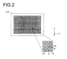
- FIG. 2 is a diagram illustrating the arrangement of pixels and unit regions 131 at the imaging chip 113. Particularly, FIG. 2 shows an appearance of the imaging chip 113 as seen from the backside.
- the pixel region for instance, 20,000,000 or more pixels are arranged in a matrix.
- adjacent 4 pixels x 4 pixels i.e., 16 pixels form one unit region 131.
- Grid lines in FIG. 2 illustrate a concept that adjacent pixels are grouped to form one unit region 131.
- the number of pixels forming each the unit region 131 is not limited to 16, but may be about 1,000, for instance, 32 pixels x 64 pixels, or more or smaller than this (for instance 1 pixel).
- each unit region 131 includes four so-called Bayer arrangements arranged up, down, left and right, each consisting of four pixels, i.e., green pixels Gb, Gr, blue pixel B, and red pixel R.
- the green pixels are pixels having a green filter as the color filter 102, receiving light in green light wavelength range out of the incident light.
- the blue pixel is a pixel having a blue filter as the color filter 102, receiving light in a blue wavelength range
- the red pixel is a pixel that has a red filter as the color filter 102, receiving light in a red wavelength range.
- a plurality of blocks is defined such that each block contains at least one unit region 131.
- the pixels contained in respective blocks are controlled by control parameters different from each other. That is, image signals under different imaging conditions may be obtained from the pixel group in one block and the pixel group in another block.
- the control parameter includes frame rate, gain, subsampling or culling rate, number of addition rows or number of addition columns in which pixel signal is to be added, time length or number of times in which charge is accumulated, and bit number in digitization and so on.
- the control parameters may be parameters that are used in image processing after the image signal is acquired from the pixel.
- FIG. 3 is a circuit diagram corresponding to the unit region 131 of the imaging chip 113.
- a rectangle which is circled in dotted line as a representative, indicates a circuit corresponding to one pixel.
- At least a portion of the transistors described below corresponds to the transistor 105 shown in FIG. 1 .
- one unit region 131 is formed by 16 pixels.
- Sixteen PDs 104 corresponding to the respective pixels are each connected to a transfer transistor 302.
- the gate of each transfer transistor 302 is connected to a TX interconnection 307, to which transfer pulses are supplied.
- one TX interconnection 307 is connected to the 16 transfer transistors 302 in common.
- each transfer transistor 302 is connected to the source of each corresponding reset transistor 303.
- a so-called floating diffusion FD between the drain of the transfer transistor 302 and the source of the reset transistor 303 is connected to the gate of an amplifying transistor 304.
- the drain of the reset transistor 303 is connected to a Vdd interconnection 310, which supplied with power-supply voltage, and the gate of the reset transistor 303 is connected to the reset interconnection 306, to which is supplied a reset pulse.
- one reset interconnection 306 is connected to the 16 reset transistors 303 in common.
- each amplifying transistor 304 is connected to a Vdd interconnection 310, to which is supplied power-supply voltage.
- the source of each amplifying transistor 304 is connected to the drain of each corresponding transistor 305.
- Each gate of the selection transistors is connected to a decoder interconnection 308, to which a selection pulse is supplied.
- the decoder interconnection 308 is provided to each of the 16 selection transistors 305 independently.
- the source of each selection transistor 305 is connected to a common output interconnection 309.
- a load current source 311 supplies current to the output interconnection 309. That is, the output interconnection 309 for the selection transistor 305 is formed by a source follower.
- the load current source 311 may be provided at the imaging chip 113 or at the signal processing chip 111.
- the PD 104 converts the received incident light into charge and accumulates the resultant charge. Then, a transfer pulse is applied again in a state where no reset pulse is applied, the accumulated charge is transferred to the floating diffusion FD. This changes the electric potential of the flowing diffusion FD from the reset potential to a signal potential after the accumulation of charge.
- a selection pulse is applied to the selection transistor 305 via the decoder interconnection 308, a variation in the signal potential of the floating diffusion FD is transferred to the output interconnection 309 via the amplifying transistor 304 and the selection transistor 305. This causes respective pixel signals corresponding to the reset potential and the signal potential to be output from the unit pixels to the output interconnection 309.
- one reset interconnection 306 and one TX interconnection 307 are provided in common. That is, the reset pulse and the transfer pulse are each applied to all the 16 pixels at the same time. Therefore, all the pixels that form one unit region 131 start the accumulation of charges at the same timing and complete the accumulation of charges at the same timing.
- the pixel signals corresponding to the accumulated charges are selectively output from the output interconnection 309 by sequentially applying selection pulses to the selection transistors 305, respectively.
- the reset interconnection 306, the TX interconnection 307, and the output interconnection 309 are provided at each unit region 131 separately.
- Arranging circuits on the basis of the unit region 131 enables control of time of charge accumulation for each unit region 131. In other words, it is possible to cause the pixel signals to be output at different frame rates from different unit regions 131. Furthermore, while the accumulation of charge in one unit region 131 is being performed once, the accumulation of charge in another unit region 131 may be performed in a plurality of times repeatedly to output a pixel signal for each time. This enables these unit regions 131 to output frames for a movie at different frame rates.
- FIG. 4 is a block diagram illustrating the functional configuration of the image sensor 100.
- An analog multiplexer 411 sequentially selects sixteen PDs 104 that form a specified unit region 131 and outputs respective pixel signals to the output interconnection 309 provided in correspondence to the specified unit region 131.
- the multiplexer 411 together with the PD 104 is formed at the imaging chip 113.
- the image signal output via the multiplexer 411 is processed by a signal processing circuit 412, which is provided at the signal processing chip 111 and performs correlated double sampling (CDS) analog/digital (A/D) conversion, to perform CDS and A/D conversion.
- CDS correlated double sampling
- A/D analog/digital
- the pixel signals subjected to the A/D conversion are passed over to a demultiplexer 413 and stored at pixel memories 414 that correspond to the respective pixels.
- the demultiplexer 413 and the pixel memories 414 are formed at the memory chip 112.
- the operation circuit 415 processes the pixel signal stored at the pixel memory 414 and passes the processed signal to a subsequent image processing unit.
- the operation circuit 415 may be provided at the signal processing chip 111 or at the memory chip 112.
- FIG. 4 shows connections for a single unit region 131. Actually, such connections are provided for each unit region 131 to enable parallel operations.
- the operation circuits 41 need not be provided for each unit region 131. For instance, one operation circuit 415 may perform sequential operation by referring to values stored at the pixel memories 414 corresponding to the respective unit regions 131.
- output interconnections 309 are provided in correspondence to the unit regions 131, respectively.
- the image sensor 100 includes the imaging chip 113, the signal processing chip 111, and the memory chip 112 stacked one on another. Consequently, use of electrical connection between the chips with bump 109 as the output interconnection 309 allows arranging the interconnections without an increase in size of each chip in the planar direction.
- FIG. 5 is a block diagram showing the arrangement of the imaging device 1 having the above-mentioned image sensor 100 taken as an example.
- the imaging device 1 includes an imaging optical system 10, an imaging unit 20, an image processing unit 30, a working memory 40, a display unit 50, a storage unit 60, and a control unit 70.
- the imaging optical system 10 includes a plurality of lenses and conducts light flux from the field to the imaging unit 20.
- the imaging optical system 10 may be arranged integrally with the imaging device 1 or interchangeable with the imaging device 1.
- the imaging optical system 10 may include a built-in focus lens or a built-in zoom lens.
- the imaging unit 20 includes the above-mentioned image sensor 100 and a drive unit 21 that drives the image sensor 100.
- the image sensor 100 is controlled for its drive with a control signal output from the drive unit 21 to enable independent control of accumulation of charge on the basis of block as mentioned above.
- the control unit 70 sends instructions with respect to the position, shape, and range of the above-mentioned blocks to the drive unit 21.
- the image processing unit 30 in cooperation with the working memory 40 performs image processing on the image data acquired by the imaging unit 20.
- the image processing unit 30 performs ordinary image processing (including color signal processing, gamma correction, etc.) and in addition detection processing for detecting a main subject contained in the image.
- the detection of the main subject by the image processing unit 30 can be performed using a known face detection function.
- the image processing unit 30 may be configured to detect, in addition to a face, a human body contained in the image as a main subject as disclosed in JP 2010-16621 A ( US 2010/0002940 ).
- the working memory 40 temporarily stores, for instance, image data before and after JPEG compression or image data before and after MPEG compression.
- the display unit 50 which includes, for instance, a liquid crystal display panel 51, displays images (still images or movie images) captured by the imaging unit 20 and various types of information or displays an input operation screen.
- the display 50 has an arrangement that includes a liquid crystal display panel 51 and a touch panel 52 stacked on a display surface of the liquid crystal display panel 51.
- the touch panel 52 outputs a signal that indicates the position of the liquid crystal display panel 51 at which the user touches.
- the storage unit 60 stores various types of data such as image data at a storage medium such as a memory card.
- the control unit 70 which has a CPU, controls operations in whole of the imaging device 1.
- the control unit 70 divides the imaging area of the image sensor 100 (imaging chip 113) into a plurality of blocks and causes different blocks to capture images at different frame rates and gains.
- the control unit 70 sends instructions with respect to the position, shape, and range of the blocks and respective control parameters for the blocks to the drive unit 21.
- the control unit 70 causes the AF operation unit 71 to calculate a focus adjustment state achieved by the imaging optical system 10.
- the control unit 70 further causes the AE, AWB operation unit 72 to perform exposure calculation to enable proper exposure to be obtained.
- FIG. 6 is a diagram showing an example of the arrangement of AF regions and AE regions at the image sensor 100 (imaging chip 113).
- shaded portions indicate AE regions and non-shaded portions indicate AF regions.
- it is set in advance so that the AF regions and the AE regions are arranged in a checkerboard pattern.
- the control unit 70 for instance, upon capturing a live view image, performs focus detection processing at the AF operation unit 71 using signals output from the AF regions of the image sensor 100.
- the live view image which is called also a preview image before main imaging is performed, refers to an image for monitoring acquired by the image sensor 100 at a predetermined frame rate (for instance, 30 fps).
- the focus detection processing is performed by, for instance, a contrast detection method. Specifically, while the position of the focus lens is being moved, the position of the focus lens of the imaging optical system 10 is adjusted so as to increase the contrast of the image constituted by signals output from the AF regions.
- the focus detection processing may be performed by a phase difference detection method.
- pixels for focus detection are arranged in the AF regions of the image sensor 100 (imaging chip 113).
- phase difference detection calculation is performed using the signals output from the pixels for focus detection to detect a focus adjustment state (specifically, a defocus amount) by the imaging optical system 10.
- the focus detection pixels and the phase difference detection calculation are known as disclosed in JP 2009-94881 A , and their detailed explanations are omitted.
- the control unit 70 performs exposure operation processing at the AE, AWB operation unit 72 using the signals output from the AE regions upon capturing the live view image.
- the AE, AWB operation unit 72 determines exposure (frame rate, gain, etc.) so that an average level of signals output from, for instance, the AE regions can become closer to a predetermined level.
- the control unit 70 also determines a white balance adjustment value based on the signals output from the AE regions.
- the control unit 70 creates an image for monitoring based on the signals output from the AE regions and causes the created image to be brought up on display as the live view image at the display unit 50.
- the control unit 70 upon capturing a live view image, sends an instruction to the drive unit 21, causing the image sensor 100 (imaging chip 113) to be divided into the AF regions and the AE regions for controlling charge accumulation.
- the control of charge accumulation for the AF regions and the AE regions dividedly is performed before main imaging (still image storage and movie storage) is instructed via a release switch (not shown).
- the frame rate is set, for instance, 120 fps and the gain is set higher than the gain for the AE regions.
- the frame rate is set at, for instance, 30 fps, which is lower than the frame rate for the AF regions and the gain is set lower than the gain for the AF regions.
- the arrangement of the AF regions and the AE regions at the image sensor 100 is not limited to the one shown in FIG. 6 as an example and the individual sizes of the AF regions and the AE regions may be changed as appropriate.
- the individual sizes of the AF regions and the AE regions may be smaller as shown in FIG.7 than those shown in FIG.6 or larger than those shown in FIG. 6 .
- FIG. 8 is a diagram illustrating an example of the case in which the area of the AF regions is made larger than the area of the AE regions and the area ratio of the AF regions to the AE regions is changed to some extent.
- the live view image mentioned above is created by subsampling or culling a portion of the pixels of the image sensor 100 and consequently, for instance, setting the AF regions in correspondence to the subsampled or culled pixels and setting the AE regions in correspondence to the pixels for live view image avoids deterioration of the image quality of the live view image.
- the AF regions may be set at predetermined size and arranged only at predetermined position of the screen.
- FIG. 9 is a flowchart illustrating the flow of imaging operation that the control unit 70 of the imaging device 1 executes in the first embodiment.
- the control unit 70 starts up the processing illustrated in FIG. 9 repeatedly if an ON-OFF switch (not shown) is turned on and current is applied to each unit of the imaging device 1.
- the control unit 70 determines control parameters for the AF regions and the AE regions, such as frame rate and gain and causes the operation to proceed to step S102. For instance, values applied in steps S102, S104, and S105 described later are provided by reading out them from the program data.
- step S102 the control unit 70 sends an instruction to the drive unit 21 to cause the imaging unit 20 to start imaging.
- the acquisition of image started in step S102 is performed by selecting, for instance, substantially the whole imaging area as the AE regions and setting control parameter for the AE regions.
- the control unit 70 causes the live view image data based on the signals output from the imaging unit 20 to be subjected to image processing by the image processing unit 30 and then causes the processed image data to be brought up on display at the display unit 50.
- step S103 the control unit 70 determines whether a release half-push operation is done.
- the release half-push operation is used as an instruction to the imaging device 1 to start pretreatment before main imaging (preparation for photographing). If the release button (not shown) is half-pushed, the control unit 70 makes a positive decision in step S103 and causes the operation to proceed to step S104. If no half-push operation is done, the control unit 70 makes a negative decision in step S103 and causes the decision operation to be repeated. To repeat the decision processing, it is awaited that a release half-push operation is done.
- the processing in step S103 may be omitted.
- the control unit 70 causes power to turn on to start up the processing illustrated in FIG. 9 and then the processing from the start up of the imaging in step S102 to the processing in steps S104 and S105 described later to be performed to apply different control parameters (frame rate and gain) to the AF regions and the AE regions that are determined in advance as shown in FIG. 6 .
- control unit 70 may be configured to cause processing similar to the tap operation to release icon to be performed or may cause pretreatment before main imaging (preparation of imaging) to be performed within several seconds after the movie switch is turned on.
- step S104 the control unit 70 sends an instruction to the drive unit 21 to cause it to apply control parameters such as frame rate and gain for the AF regions to the AF regions of the image sensor 100.
- step S105 the control unit 70 sends an instruction to the drive unit 21 to cause it to apply control parameters such as frame rate and gain for the AE regions to the AE regions of the image sensor 100.
- the control unit 70 causes, based on signals output from the AE regions at the above-mentioned frame rate, minute adjustment of the control parameters, determination of white balance adjustment value, and bringing up on display of the live view image to be performed.
- step S106 the control unit 70 starts up the AF processing. Specifically, the control unit 70 causes the AF operation unit 71 to start focus detection processing based on the signals output from the AF regions and causes the operation to proceed to step S107. This enables focus adjustment of the imaging optical system 10 based on the signals output from the AF regions at the above-mentioned frame rate.
- step S107 the control unit 70 makes a decision whether the AF processing is completed.
- the control unit 70 makes a positive decision in step S107 if, for instance, the contrast of the image obtained from the AF regions is equal to or higher than a predetermined value whereas it makes a negative decision in step S107 if the contrast of the image obtained from the AF regions is below the predetermined value. In case it makes a negative decision, it causes the decision making processing to be repeated while it causes the focus detection processing to be continued.
- step S108 the control unit 70, based on signals output from the AE regions after the focus adjustment, causes the AE, AWB operation unit 72 to calculate exposure conditions and white balance adjustment value to be applied at the time of imaging and causes the operation to proceed to step S109.
- step S109 the control unit 70 makes a decision whether a release complete-push operation is performed.
- the release complete-push operation is used as an instruction for main imaging to the imaging device 1.
- the control unit 70 makes a positive decision in step S109 if the release button (not shown) is subjected to a complete-push operation and causes the operation to proceed to step S110 and makes a negative decision in S109 if the release button is not subjected to a complete-push operation and causes the operation to return to step S108. If the operation returns to step S108, the above-mentioned processing is repeated.
- the control unit 70 cancels the imaging by the imaging unit 20 using the control parameters for the AF regions and the control parameters for the AE regions if the release button (not shown) is subjected to a complete-push operation.
- a positive decision in step S109 is made when a tap operation is made to the release icon that is brought up on display.
- step S110 the control unit 70 sends an instruction to the drive unit 21 to cause control parameters (exposure time, gain, etc.) necessary for exposure conditions for imaging calculated in step S108 to be set and causes the operation to proceed to step S111.
- control parameters exposure time, gain, etc.
- step S111 the control unit 70 executes imaging processing and causes the storage unit 60 to store data of the acquired image at, for instance, a memory card and causes the processing illustrated in FIG. 9 to end.
- the imaging processing one frame of still image is acquired (main imaging) by applying control parameters for imaging that are set common (same) for all the regions at the image sensor 100 and the acquired image is stored.
- a plurality of frames of image is acquired.
- the control unit 70 may be configured to change, if a portion of the field contains a high brightness subject, imaging conditions of pixels corresponding to the high brightness subject.
- slow motion reproduction movie data is created and stored.
- the slow motion reproduction movie data means movie data reproduced at a frame rate (for instance, 15 fps), which is slower than the frame rate at which the image is acquired (for instance, 30 fps) by the image sensor 100.
- the control unit 70 creates slow motion reproduction movie data as follows. That is, slow motion reproduction movie data is created based on a plurality of frame images based on the AE regions temporarily stored at the working memory for displaying the live view image from a time by a first predetermined time (for instance, 0.6 seconds) earlier than time of release complete-push operation (say, t1) to time t1 (the frame rate being the frame rate set for the AE regions, with frames acquired at 30 fps for 0.6 seconds giving 18 frames) and a plurality of frame images stored at the working memory 40 from time t1 to a time by a second predetermined time (for instance, 0.4 seconds) later than time t1 (with the frame rate being the same as the frame rate set for the AE regions prior to the instruction for main imaging, with frames acquired at 30 fps for 0.4 seconds giving 12 frames).
- a first predetermined time for instance, 0.6 seconds
- time of release complete-push operation say, t1
- time t1 the frame rate being the frame
- slow motion reproduction movie data reproduction of which takes about 2 seconds
- a plurality of frame images total 30 frames stored at the working memory 40 for 1 second sandwiching the time t1 (i.e., from a time 0.6 seconds before time t1 to a time 0.4 seconds after time t1).
- the slow motion movie data is obtained based on the respective frame images acquired before and after the release complete-push operation.
- the slow motion movie data is created by the image processing unit 30 as MPEG data or JPEG data.
- FIG. 10 is a diagram illustrating the relationship between the AF regions and AE regions and the live view image according to the second embodiment.
- a person is contained short of the center of the live view image
- trees are contained in the left upper part of the live view image
- in the right upper part of the live view image is contained the sun.
- the control unit 70 sends an instruction to the image processing unit 30 to cause the image processing unit 30 to perform known scene recognition processing to the live view image data.
- the image processing unit 30 performs scene recognition processing to extract a high brightness region A, a main subject region B, and a background region C from the live view image.
- the image processing unit 30 determines, for instance, a range of the live view image data in which the signal level exceeds a predetermined high brightness threshold value to be a high brightness region A.
- the image processing unit 30 determines a range in which a human body detected as described above is contained to be a main subject region B.
- the image processing unit 30 may be configured to detect not only a person but also an animal such as a pet and determine a range in which the animal is contained to be the main subject region B.
- the image processing unit 30 is further configured to perform edge detection at a position excluding the high brightness region A and the main subject region B and determine a range in which the density of the detected edge exceeds a predetermined value to be a background region C. If no live view image data has a value that exceeds the high brightness threshold value, the image processing unit 30 determines that no high brightness region A is present.
- the control unit 70 causes the AF regions and the AE regions in the main subject region B to be arranged in a checkerboard pattern.
- the shaded part in the main subject region B represents the AE regions and non-shaded part represents the AF regions.
- the arrangement of the AF regions and the AE regions in the main subject region B is not limited to the one shown in FIG. 10 as an example.
- the sizes of the AF regions and the AE regions may be individually changed as appropriate. Not only may the sizes of the AF regions and the AE regions but also the area ratio be changed such that the area of the AE regions is larger than the area of the AF regions.
- the AF regions with a predetermined size may be arranged only at the predetermined position.
- the control unit 70 may be configured to cause the AF regions and the AE regions to be arranged such that portions of the AF regions and the AE regions protrude outside the main subject region B.
- the control unit 70 determines the background region C to be an AE region.
- the shaded part in the background region C represents an AE region.
- the control unit 70 determines neither AF regions nor AE regions for portions having a threshold value that exceeds the high brightness threshold value (high brightness region A in the example shown in FIG. 10 ).
- the portion with vertical lines in the high brightness region represents neither AF region nor AE region.
- the control unit 70 is configured to determine region other than the regions A, B and C of the live view image screen (blank portion in FIG. 10 ) to be AE regions.
- FIG. 11 is a diagram illustrating the three settings.
- Setting 1 is to set control parameters (frame rate, gain, etc.) suitable for high brightness for high brightness region A (that is, neither AF area nor AE region) so as to avoid saturation of output signal by, for instance, increasing frame rate and decreasing gain.
- Setting 2 is to control parameters (frame rate, gain, etc.) suitable for focus detection processing for the AF regions at the main subject region B in the same manner as that in the first embodiment and to set control parameters (frame rate, gain, etc.) suitable for exposure calculation processing for the AE regions at the main subject region B in the same manner as that in the first embodiment.
- Setting 3 is to set control parameters (frame rate, gain, etc.) suitable for exposure calculation processing for the background region C and the region that belongs neither to the high brightness region A nor the main subject region B (blank portion in FIG. 10 ) in the same manner as that in the AE regions in the main subject region B.
- the control unit 70 sends an instruction to the drive unit 21 to cause the above three settings to be made on the image sensor 100 (imaging chip 113).
- This allows the image sensor 100 (imaging chip 113) to be controlled for charge accumulation with different control parameters (frame rate, gain, etc.) for the AF regions, AE regions and the region other than the AF regions and the AE regions upon capturing the live view image.
- Control of charge accumulation is performed, for instance, from a time after the scene recognition by the image processing unit 30 to a time in which main imaging is instructed.
- the control parameters for the AF regions include, for instance, a frame rate of 120 fps and gain that is higher in the AE regions than the AF regions.
- the control parameters for the AE regions include, for instance, a frame rate of 30 fps, which is lower than the frame rate for the AF regions, and a gain of the AE regions being lower than the gain of the AF regions.
- Applying to the AF regions a frame rate higher than the frame rate applied to the AE regions to acquire images for focus detection processing is intended to improve the responsiveness of the focus detection processing.
- a gain lower than that applied to the AF regions is intended to perform high precision calculation avoiding the influence of noises.
- control parameters for the region other than the AF regions and the AE regions include, for instance, a frame rate of 60 fps and a gain lower than that applied to the AE regions. This enables image of high brightness subject that would cause clipped whites to be captured without causing any clipped whites.
- FIG. 12 is a flowchart illustrating the flow of imaging processing executed by the control unit 70 of the imaging device 1 according to the second embodiment.
- the flowchart relating to the second embodiment differs from the flowchart relating to the first embodiment illustrated in FIG. 9 in the processing in steps S104B and S105B. Explanation is focused on these differences.
- Capturing of image started in step S102 in FIG. 12 is performed by determining substantially the whole area of the imaging plane to be AE regions and setting control parameters for the AE regions in the same manner as that in the case shown in FIG. 9 .
- the control unit 70 determines the live view image data based on signals output from the imaging unit 20 by the above-mentioned settings to be a subject of scene recognition.
- the control unit 70 sends an instruction to the image processing unit 30 to cause it to perform known scene recognition processing on the live view image data.
- the image processing unit 30 performs the scene recognition processing to divide the screen into the high brightness region A, the main subject region B, and the background region C as described above.
- step S105B the control unit 70 sends an instruction to the drive unit 21 to cause the above-mentioned three settings to be performed for each divided region.
- This allows applying different control parameters to the AF regions, the AE regions, the region other than the AF regions and the AE regions to obtain different images.
- the control unit 70 is capable of performing minute adjustment of control parameters and determining a white balance adjustment value based on the images acquired from the AE regions.
- the live view image may be displayed based on the images acquired at the AE regions and the region other than the AF regions and the AE regions.
- the imaging device 1 according to the first embodiment or the second embodiment may be constituted by a high functionality mobile phone or a tablet terminal.
- the camera unit installed at the high functionality mobile phone (or tablet terminal) is constituted with the stacked image sensor 100 mentioned above.
- an AWB region may be provided separately from the AF regions and the AE regions. Then, upon acquiring the live view image the image sensor 100 (imaging chip 113) is controlled for its accumulation of charge with different control parameters (frame rate, gain, etc.) for the AF regions, the AE regions, and the AWB region separately.
- control unit 70 causes focus detection processing to be performed based on the images acquired from the AF regions.
- the control unit 70 causes determination of white balance adjustment value based on the image acquired from the AWB region. Minute adjustment of the control parameters is performed based the images acquired from the AE regions. Display of the live view image is performed based on the image acquired from the AE regions and the image acquired from the region other than the AF regions and the AE regions.
Landscapes
- Engineering & Computer Science (AREA)
- Signal Processing (AREA)
- Multimedia (AREA)
- Physics & Mathematics (AREA)
- Power Engineering (AREA)
- Condensed Matter Physics & Semiconductors (AREA)
- Computer Hardware Design (AREA)
- Microelectronics & Electronic Packaging (AREA)
- General Physics & Mathematics (AREA)
- Electromagnetism (AREA)
- Spectroscopy & Molecular Physics (AREA)
- Studio Devices (AREA)
- Transforming Light Signals Into Electric Signals (AREA)
- Solid State Image Pick-Up Elements (AREA)
- Automatic Focus Adjustment (AREA)
Applications Claiming Priority (2)
| Application Number | Priority Date | Filing Date | Title |
|---|---|---|---|
| JP2013037617 | 2013-02-27 | ||
| PCT/JP2014/054865 WO2014133076A1 (ja) | 2013-02-27 | 2014-02-27 | 撮像素子および電子機器 |
Publications (3)
| Publication Number | Publication Date |
|---|---|
| EP2963917A1 true EP2963917A1 (de) | 2016-01-06 |
| EP2963917A4 EP2963917A4 (de) | 2016-10-19 |
| EP2963917B1 EP2963917B1 (de) | 2021-04-14 |
Family
ID=51428335
Family Applications (1)
| Application Number | Title | Priority Date | Filing Date |
|---|---|---|---|
| EP14756999.0A Active EP2963917B1 (de) | 2013-02-27 | 2014-02-27 | Elektronische vorrichtung mit einem bildsensor |
Country Status (5)
| Country | Link |
|---|---|
| US (3) | US10924697B2 (de) |
| EP (1) | EP2963917B1 (de) |
| JP (5) | JP6090425B2 (de) |
| CN (2) | CN105103537B (de) |
| WO (1) | WO2014133076A1 (de) |
Cited By (1)
| Publication number | Priority date | Publication date | Assignee | Title |
|---|---|---|---|---|
| US10244159B2 (en) | 2013-12-05 | 2019-03-26 | Canon Kabushiki Kaisha | Image capturing apparatus and control method thereof |
Families Citing this family (23)
| Publication number | Priority date | Publication date | Assignee | Title |
|---|---|---|---|---|
| CN105103537B (zh) * | 2013-02-27 | 2018-11-06 | 株式会社尼康 | 成像元件及电子设备 |
| JP6234058B2 (ja) * | 2013-05-09 | 2017-11-22 | キヤノン株式会社 | 焦点調節装置およびその制御方法 |
| EP3076662A4 (de) | 2013-11-26 | 2017-08-09 | Nikon Corporation | Elektronische vorrichtung, bildgebungsvorrichtung und bildgebungselement |
| JP6198600B2 (ja) * | 2013-12-16 | 2017-09-20 | キヤノン株式会社 | 画像処理装置、撮像装置、その制御方法及びプログラム |
| JP6146293B2 (ja) * | 2013-12-25 | 2017-06-14 | ソニー株式会社 | 制御装置、制御方法および制御システム |
| JP2015195235A (ja) * | 2014-03-31 | 2015-11-05 | ソニー株式会社 | 固体撮像素子、電子機器、および撮像方法 |
| JP2016072864A (ja) * | 2014-09-30 | 2016-05-09 | 株式会社ニコン | 電子機器、再生装置、記録媒体、記録プログラム、再生プログラム、記録方法および再生方法 |
| JP6613554B2 (ja) * | 2014-09-30 | 2019-12-04 | 株式会社ニコン | 画像処理装置およびプログラム |
| JP2016072863A (ja) * | 2014-09-30 | 2016-05-09 | 株式会社ニコン | 電子機器、再生装置、記録媒体、記録プログラム、再生プログラム、記録方法および再生方法 |
| JP2016072866A (ja) * | 2014-09-30 | 2016-05-09 | 株式会社ニコン | 電子機器、再生装置、記録媒体、記録プログラム、再生プログラム、記録方法および再生方法 |
| JP6520036B2 (ja) * | 2014-09-30 | 2019-05-29 | 株式会社ニコン | 電子機器 |
| JP6642440B2 (ja) * | 2014-09-30 | 2020-02-05 | 株式会社ニコン | 電子機器 |
| US10485486B2 (en) * | 2014-11-18 | 2019-11-26 | Baylor College Of Medicine | Clinical metric for predicting onset of cardiorespiratory deterioration in patients |
| CN112653821A (zh) * | 2014-12-03 | 2021-04-13 | 株式会社尼康 | 电子设备 |
| CN105446056B (zh) * | 2014-12-25 | 2018-08-10 | 北京展讯高科通信技术有限公司 | 自动对焦装置及方法 |
| KR102328098B1 (ko) * | 2015-02-13 | 2021-11-17 | 삼성전자주식회사 | 전자장치의 초점 검출 장치 및 방법 |
| KR20160102814A (ko) * | 2015-02-23 | 2016-08-31 | 삼성전자주식회사 | 이미지 센서 이를 포함하는 이미지 처리 시스템, 및 상기 이미지 센서를 포함하는 모바일 컴퓨팅 장치 |
| JP6608185B2 (ja) * | 2015-06-18 | 2019-11-20 | キヤノン株式会社 | 積層型イメージセンサおよび撮像装置 |
| KR20180117597A (ko) * | 2016-03-03 | 2018-10-29 | 소니 주식회사 | 화상 처리 장치, 화상 처리 방법, 컴퓨터 프로그램 및 전자 기기 |
| CN105827994A (zh) * | 2016-04-12 | 2016-08-03 | 乐视控股(北京)有限公司 | 一种解决对焦区曝光过度的系统及方法 |
| JP6808993B2 (ja) * | 2016-06-17 | 2021-01-06 | 株式会社ニコン | 撮像素子、電子機器、撮像方法、およびプログラム |
| US10491832B2 (en) * | 2017-08-16 | 2019-11-26 | Qualcomm Incorporated | Image capture device with stabilized exposure or white balance |
| JP6686122B1 (ja) * | 2018-12-21 | 2020-04-22 | 株式会社モルフォ | 画像処理装置、画像処理方法およびプログラム |
Family Cites Families (48)
| Publication number | Priority date | Publication date | Assignee | Title |
|---|---|---|---|---|
| JPH03243071A (ja) * | 1990-02-21 | 1991-10-30 | Sony Corp | オートフォーカス回路 |
| JPH06303379A (ja) | 1993-04-14 | 1994-10-28 | Fuji Xerox Co Ltd | 画像読取素子 |
| JP3270252B2 (ja) * | 1994-09-12 | 2002-04-02 | オリンパス光学工業株式会社 | カメラ |
| JPH0918773A (ja) * | 1995-06-27 | 1997-01-17 | Canon Inc | 撮像装置 |
| JP4100736B2 (ja) | 1996-09-27 | 2008-06-11 | シャープ株式会社 | 非水系二次電池用正極活物質ニッケル酸リチウムの製造方法 |
| JP2002116369A (ja) * | 2000-10-05 | 2002-04-19 | Ricoh Co Ltd | 自動焦点制御装置 |
| JP2003289469A (ja) * | 2002-03-28 | 2003-10-10 | Minolta Co Ltd | 撮像装置 |
| JP2003333506A (ja) * | 2002-05-10 | 2003-11-21 | Canon Inc | 画像処理装置、画像処理システム、画像処理方法、プログラム、及び記憶媒体 |
| US6747808B2 (en) * | 2002-10-04 | 2004-06-08 | Hewlett-Packard Development Company, L.P. | Electronic imaging device focusing |
| JP4665422B2 (ja) | 2004-04-02 | 2011-04-06 | ソニー株式会社 | 撮像装置 |
| JP4612814B2 (ja) * | 2004-07-26 | 2011-01-12 | キヤノン株式会社 | 自動焦点調節装置及びその制御方法並びに撮像装置 |
| JP4349232B2 (ja) | 2004-07-30 | 2009-10-21 | ソニー株式会社 | 半導体モジュール及びmos型固体撮像装置 |
| JP2006109103A (ja) | 2004-10-05 | 2006-04-20 | Victor Co Of Japan Ltd | 撮像装置のフォーカス処理回路 |
| JP2006303755A (ja) * | 2005-04-19 | 2006-11-02 | Konica Minolta Photo Imaging Inc | 撮像装置及び撮像方法 |
| TW201101476A (en) | 2005-06-02 | 2011-01-01 | Sony Corp | Semiconductor image sensor module and method of manufacturing the same |
| JP4218670B2 (ja) * | 2005-09-27 | 2009-02-04 | オムロン株式会社 | 前方撮影装置 |
| JP4816336B2 (ja) * | 2006-02-07 | 2011-11-16 | 日本ビクター株式会社 | 撮像方法及び撮像装置 |
| JP2007228019A (ja) * | 2006-02-21 | 2007-09-06 | Olympus Corp | 撮像装置 |
| JP2007248782A (ja) * | 2006-03-15 | 2007-09-27 | Olympus Imaging Corp | 焦点調節装置およびカメラ |
| US8049801B2 (en) * | 2006-09-14 | 2011-11-01 | Nikon Corporation | Image sensor and imaging apparatus |
| US8031258B2 (en) * | 2006-10-04 | 2011-10-04 | Omnivision Technologies, Inc. | Providing multiple video signals from single sensor |
| JP2009049858A (ja) * | 2007-08-22 | 2009-03-05 | Canon Inc | 撮像装置 |
| JP5009091B2 (ja) * | 2007-08-23 | 2012-08-22 | 富士フイルム株式会社 | 焦点調節装置及び焦点調節方法 |
| JP5056297B2 (ja) * | 2007-09-14 | 2012-10-24 | カシオ計算機株式会社 | 撮像装置、撮像装置制御プログラム及び撮像装置制御方法 |
| JP5194688B2 (ja) | 2007-10-01 | 2013-05-08 | 株式会社ニコン | 固体撮像装置 |
| JP5029274B2 (ja) | 2007-10-10 | 2012-09-19 | 株式会社ニコン | 撮像装置 |
| JP2009141631A (ja) * | 2007-12-05 | 2009-06-25 | Canon Inc | 光電変換装置及び撮像装置 |
| US8441535B2 (en) * | 2008-03-05 | 2013-05-14 | Omnivision Technologies, Inc. | System and method for independent image sensor parameter control in regions of interest |
| JP4530067B2 (ja) * | 2008-03-27 | 2010-08-25 | ソニー株式会社 | 撮像装置、撮像方法及びプログラム |
| US7667169B2 (en) | 2008-05-22 | 2010-02-23 | Omnivision Technologies, Inc. | Image sensor with simultaneous auto-focus and image preview |
| JP2010016621A (ja) | 2008-07-03 | 2010-01-21 | Sony Corp | 画像データ処理装置と画像データ処理方法およびプログラムと記録媒体 |
| JP5266916B2 (ja) * | 2008-07-09 | 2013-08-21 | ソニー株式会社 | 撮像素子、カメラ、撮像素子の制御方法、並びにプログラム |
| JP2010020015A (ja) * | 2008-07-09 | 2010-01-28 | Canon Inc | 撮像装置 |
| US8179466B2 (en) * | 2009-03-11 | 2012-05-15 | Eastman Kodak Company | Capture of video with motion-speed determination and variable capture rate |
| JP5238673B2 (ja) * | 2009-11-09 | 2013-07-17 | 株式会社東芝 | 固体撮像装置 |
| KR101624654B1 (ko) * | 2010-03-15 | 2016-05-26 | 삼성전자주식회사 | 초점 조절 장치 및 초점 조절 방법 |
| JP5541016B2 (ja) | 2010-09-08 | 2014-07-09 | リコーイメージング株式会社 | 撮像システムおよび画素信号読出し方法 |
| JP5633323B2 (ja) | 2010-11-11 | 2014-12-03 | ソニー株式会社 | 固体撮像装置及び電子機器 |
| JP2012129425A (ja) * | 2010-12-16 | 2012-07-05 | Canon Inc | マトリクス基板、検出装置、検出システム、及び、検出装置の駆動方法 |
| JP5653207B2 (ja) | 2010-12-27 | 2015-01-14 | アルパイン株式会社 | 消費電力制御システム |
| JP2012175234A (ja) | 2011-02-18 | 2012-09-10 | Sony Corp | 撮像装置、撮像素子、および撮像制御方法、並びにプログラム |
| US20130002936A1 (en) * | 2011-06-30 | 2013-01-03 | Nikon Corporation | Image pickup apparatus, image processing apparatus, and storage medium storing image processing program |
| JP2013145779A (ja) * | 2012-01-13 | 2013-07-25 | Sony Corp | 固体撮像装置及び電子機器 |
| JP2013172210A (ja) * | 2012-02-17 | 2013-09-02 | Canon Inc | 撮像装置 |
| JP6023437B2 (ja) * | 2012-02-29 | 2016-11-09 | キヤノン株式会社 | 固体撮像装置及びカメラ |
| EP2846538B1 (de) | 2012-05-02 | 2021-06-23 | Nikon Corporation | Bildgebungsvorrichtung |
| CN105103537B (zh) * | 2013-02-27 | 2018-11-06 | 株式会社尼康 | 成像元件及电子设备 |
| US9661243B2 (en) * | 2013-03-15 | 2017-05-23 | Forza Silicon Corporation | CMOS image sensor with column-wise selective charge-domain binning |
-
2014
- 2014-02-27 CN CN201480010575.XA patent/CN105103537B/zh active Active
- 2014-02-27 EP EP14756999.0A patent/EP2963917B1/de active Active
- 2014-02-27 CN CN201811159203.XA patent/CN109348148B/zh active Active
- 2014-02-27 JP JP2015503018A patent/JP6090425B2/ja active Active
- 2014-02-27 US US14/771,123 patent/US10924697B2/en active Active
- 2014-02-27 WO PCT/JP2014/054865 patent/WO2014133076A1/ja active Application Filing
-
2017
- 2017-02-09 JP JP2017022351A patent/JP2017118579A/ja active Pending
-
2019
- 2019-10-09 JP JP2019185900A patent/JP2020036330A/ja active Pending
-
2021
- 2021-01-12 US US17/146,870 patent/US11595604B2/en active Active
- 2021-07-20 JP JP2021119878A patent/JP7264189B2/ja active Active
-
2023
- 2023-02-02 US US18/104,936 patent/US20230199343A1/en active Pending
- 2023-04-12 JP JP2023064809A patent/JP2023089131A/ja active Pending
Cited By (1)
| Publication number | Priority date | Publication date | Assignee | Title |
|---|---|---|---|---|
| US10244159B2 (en) | 2013-12-05 | 2019-03-26 | Canon Kabushiki Kaisha | Image capturing apparatus and control method thereof |
Also Published As
| Publication number | Publication date |
|---|---|
| EP2963917A4 (de) | 2016-10-19 |
| EP2963917B1 (de) | 2021-04-14 |
| JP2021168512A (ja) | 2021-10-21 |
| CN109348148A (zh) | 2019-02-15 |
| CN105103537A (zh) | 2015-11-25 |
| US10924697B2 (en) | 2021-02-16 |
| JP2023089131A (ja) | 2023-06-27 |
| CN109348148B (zh) | 2022-03-15 |
| JPWO2014133076A1 (ja) | 2017-02-02 |
| US11595604B2 (en) | 2023-02-28 |
| US20210136302A1 (en) | 2021-05-06 |
| JP6090425B2 (ja) | 2017-03-08 |
| US20160014359A1 (en) | 2016-01-14 |
| JP2017118579A (ja) | 2017-06-29 |
| CN105103537B (zh) | 2018-11-06 |
| JP2020036330A (ja) | 2020-03-05 |
| WO2014133076A1 (ja) | 2014-09-04 |
| US20230199343A1 (en) | 2023-06-22 |
| JP7264189B2 (ja) | 2023-04-25 |
Similar Documents
| Publication | Publication Date | Title |
|---|---|---|
| US11595604B2 (en) | Image sensor and imaging device including a plurality of semiconductor substrates | |
| JP6780745B2 (ja) | 電子機器 | |
| CN110086980B (zh) | 电子设备 | |
| CN110365909B (zh) | 电子设备 | |
| JP2014178603A (ja) | 撮像装置 | |
| JP6561428B2 (ja) | 電子機器、制御方法、及び制御プログラム | |
| JP2014179892A (ja) | 撮像装置 | |
| US20180213140A1 (en) | Electronic device, imaging device, and imaging element | |
| EP2975839B1 (de) | Bilderfassungseinheit, bilderfassungsvorrichtung und bilderfassungssteuerungsprogramm | |
| JP2014179778A (ja) | 信号処理装置、撮像素子、撮像装置および電子機器 | |
| US10686987B2 (en) | Electronic apparatus with image capturing unit having first and second imaging regions that capture an image of a subject under differing imaging conditions | |
| JP6781140B2 (ja) | 撮像装置 | |
| US20170324911A1 (en) | Electronic apparatus, reproduction device, reproduction method, recording medium, and recording method | |
| JP6852712B2 (ja) | 撮像素子および撮像装置 | |
| JP7176591B2 (ja) | 電子機器 | |
| JP6349659B2 (ja) | 電子機器、電子機器の制御方法、及び制御プログラム | |
| JP2021193811A (ja) | 撮像素子、及び撮像装置 |
Legal Events
| Date | Code | Title | Description |
|---|---|---|---|
| PUAI | Public reference made under article 153(3) epc to a published international application that has entered the european phase |
Free format text: ORIGINAL CODE: 0009012 |
|
| 17P | Request for examination filed |
Effective date: 20150826 |
|
| AK | Designated contracting states |
Kind code of ref document: A1 Designated state(s): AL AT BE BG CH CY CZ DE DK EE ES FI FR GB GR HR HU IE IS IT LI LT LU LV MC MK MT NL NO PL PT RO RS SE SI SK SM TR |
|
| AX | Request for extension of the european patent |
Extension state: BA ME |
|
| DAX | Request for extension of the european patent (deleted) | ||
| A4 | Supplementary search report drawn up and despatched |
Effective date: 20160921 |
|
| RIC1 | Information provided on ipc code assigned before grant |
Ipc: H04N 5/235 20060101ALI20160915BHEP Ipc: H04N 5/353 20110101ALI20160915BHEP Ipc: H01L 27/146 20060101ALI20160915BHEP Ipc: H04N 5/335 20060101ALI20160915BHEP Ipc: H04N 5/345 20110101AFI20160915BHEP Ipc: H04N 5/232 20060101ALI20160915BHEP |
|
| STAA | Information on the status of an ep patent application or granted ep patent |
Free format text: STATUS: EXAMINATION IS IN PROGRESS |
|
| 17Q | First examination report despatched |
Effective date: 20190417 |
|
| REG | Reference to a national code |
Ref country code: DE Ref legal event code: R079 Ref document number: 602014076583 Country of ref document: DE Free format text: PREVIOUS MAIN CLASS: H04N0005345000 Ipc: H04N0005369000 |
|
| RIC1 | Information provided on ipc code assigned before grant |
Ipc: H04N 5/232 20060101ALI20201002BHEP Ipc: H04N 5/345 20110101ALI20201002BHEP Ipc: H04N 5/369 20110101AFI20201002BHEP Ipc: H01L 27/146 20060101ALI20201002BHEP Ipc: H04N 5/235 20060101ALI20201002BHEP |
|
| GRAP | Despatch of communication of intention to grant a patent |
Free format text: ORIGINAL CODE: EPIDOSNIGR1 |
|
| STAA | Information on the status of an ep patent application or granted ep patent |
Free format text: STATUS: GRANT OF PATENT IS INTENDED |
|
| INTG | Intention to grant announced |
Effective date: 20201117 |
|
| GRAS | Grant fee paid |
Free format text: ORIGINAL CODE: EPIDOSNIGR3 |
|
| GRAA | (expected) grant |
Free format text: ORIGINAL CODE: 0009210 |
|
| STAA | Information on the status of an ep patent application or granted ep patent |
Free format text: STATUS: THE PATENT HAS BEEN GRANTED |
|
| AK | Designated contracting states |
Kind code of ref document: B1 Designated state(s): AL AT BE BG CH CY CZ DE DK EE ES FI FR GB GR HR HU IE IS IT LI LT LU LV MC MK MT NL NO PL PT RO RS SE SI SK SM TR |
|
| REG | Reference to a national code |
Ref country code: GB Ref legal event code: FG4D |
|
| REG | Reference to a national code |
Ref country code: CH Ref legal event code: EP |
|
| REG | Reference to a national code |
Ref country code: DE Ref legal event code: R096 Ref document number: 602014076583 Country of ref document: DE |
|
| REG | Reference to a national code |
Ref country code: IE Ref legal event code: FG4D |
|
| REG | Reference to a national code |
Ref country code: AT Ref legal event code: REF Ref document number: 1383502 Country of ref document: AT Kind code of ref document: T Effective date: 20210515 |
|
| REG | Reference to a national code |
Ref country code: LT Ref legal event code: MG9D |
|
| REG | Reference to a national code |
Ref country code: AT Ref legal event code: MK05 Ref document number: 1383502 Country of ref document: AT Kind code of ref document: T Effective date: 20210414 |
|
| REG | Reference to a national code |
Ref country code: NL Ref legal event code: MP Effective date: 20210414 |
|
| PG25 | Lapsed in a contracting state [announced via postgrant information from national office to epo] |
Ref country code: NL Free format text: LAPSE BECAUSE OF FAILURE TO SUBMIT A TRANSLATION OF THE DESCRIPTION OR TO PAY THE FEE WITHIN THE PRESCRIBED TIME-LIMIT Effective date: 20210414 Ref country code: LT Free format text: LAPSE BECAUSE OF FAILURE TO SUBMIT A TRANSLATION OF THE DESCRIPTION OR TO PAY THE FEE WITHIN THE PRESCRIBED TIME-LIMIT Effective date: 20210414 Ref country code: FI Free format text: LAPSE BECAUSE OF FAILURE TO SUBMIT A TRANSLATION OF THE DESCRIPTION OR TO PAY THE FEE WITHIN THE PRESCRIBED TIME-LIMIT Effective date: 20210414 Ref country code: AT Free format text: LAPSE BECAUSE OF FAILURE TO SUBMIT A TRANSLATION OF THE DESCRIPTION OR TO PAY THE FEE WITHIN THE PRESCRIBED TIME-LIMIT Effective date: 20210414 Ref country code: BG Free format text: LAPSE BECAUSE OF FAILURE TO SUBMIT A TRANSLATION OF THE DESCRIPTION OR TO PAY THE FEE WITHIN THE PRESCRIBED TIME-LIMIT Effective date: 20210714 Ref country code: HR Free format text: LAPSE BECAUSE OF FAILURE TO SUBMIT A TRANSLATION OF THE DESCRIPTION OR TO PAY THE FEE WITHIN THE PRESCRIBED TIME-LIMIT Effective date: 20210414 |
|
| PG25 | Lapsed in a contracting state [announced via postgrant information from national office to epo] |
Ref country code: IS Free format text: LAPSE BECAUSE OF FAILURE TO SUBMIT A TRANSLATION OF THE DESCRIPTION OR TO PAY THE FEE WITHIN THE PRESCRIBED TIME-LIMIT Effective date: 20210814 Ref country code: LV Free format text: LAPSE BECAUSE OF FAILURE TO SUBMIT A TRANSLATION OF THE DESCRIPTION OR TO PAY THE FEE WITHIN THE PRESCRIBED TIME-LIMIT Effective date: 20210414 Ref country code: GR Free format text: LAPSE BECAUSE OF FAILURE TO SUBMIT A TRANSLATION OF THE DESCRIPTION OR TO PAY THE FEE WITHIN THE PRESCRIBED TIME-LIMIT Effective date: 20210715 Ref country code: ES Free format text: LAPSE BECAUSE OF FAILURE TO SUBMIT A TRANSLATION OF THE DESCRIPTION OR TO PAY THE FEE WITHIN THE PRESCRIBED TIME-LIMIT Effective date: 20210414 Ref country code: NO Free format text: LAPSE BECAUSE OF FAILURE TO SUBMIT A TRANSLATION OF THE DESCRIPTION OR TO PAY THE FEE WITHIN THE PRESCRIBED TIME-LIMIT Effective date: 20210714 Ref country code: PL Free format text: LAPSE BECAUSE OF FAILURE TO SUBMIT A TRANSLATION OF THE DESCRIPTION OR TO PAY THE FEE WITHIN THE PRESCRIBED TIME-LIMIT Effective date: 20210414 Ref country code: PT Free format text: LAPSE BECAUSE OF FAILURE TO SUBMIT A TRANSLATION OF THE DESCRIPTION OR TO PAY THE FEE WITHIN THE PRESCRIBED TIME-LIMIT Effective date: 20210816 Ref country code: RS Free format text: LAPSE BECAUSE OF FAILURE TO SUBMIT A TRANSLATION OF THE DESCRIPTION OR TO PAY THE FEE WITHIN THE PRESCRIBED TIME-LIMIT Effective date: 20210414 Ref country code: SE Free format text: LAPSE BECAUSE OF FAILURE TO SUBMIT A TRANSLATION OF THE DESCRIPTION OR TO PAY THE FEE WITHIN THE PRESCRIBED TIME-LIMIT Effective date: 20210414 |
|
| REG | Reference to a national code |
Ref country code: DE Ref legal event code: R097 Ref document number: 602014076583 Country of ref document: DE |
|
| PG25 | Lapsed in a contracting state [announced via postgrant information from national office to epo] |
Ref country code: RO Free format text: LAPSE BECAUSE OF FAILURE TO SUBMIT A TRANSLATION OF THE DESCRIPTION OR TO PAY THE FEE WITHIN THE PRESCRIBED TIME-LIMIT Effective date: 20210414 Ref country code: SK Free format text: LAPSE BECAUSE OF FAILURE TO SUBMIT A TRANSLATION OF THE DESCRIPTION OR TO PAY THE FEE WITHIN THE PRESCRIBED TIME-LIMIT Effective date: 20210414 Ref country code: SM Free format text: LAPSE BECAUSE OF FAILURE TO SUBMIT A TRANSLATION OF THE DESCRIPTION OR TO PAY THE FEE WITHIN THE PRESCRIBED TIME-LIMIT Effective date: 20210414 Ref country code: EE Free format text: LAPSE BECAUSE OF FAILURE TO SUBMIT A TRANSLATION OF THE DESCRIPTION OR TO PAY THE FEE WITHIN THE PRESCRIBED TIME-LIMIT Effective date: 20210414 Ref country code: DK Free format text: LAPSE BECAUSE OF FAILURE TO SUBMIT A TRANSLATION OF THE DESCRIPTION OR TO PAY THE FEE WITHIN THE PRESCRIBED TIME-LIMIT Effective date: 20210414 Ref country code: CZ Free format text: LAPSE BECAUSE OF FAILURE TO SUBMIT A TRANSLATION OF THE DESCRIPTION OR TO PAY THE FEE WITHIN THE PRESCRIBED TIME-LIMIT Effective date: 20210414 |
|
| PLBE | No opposition filed within time limit |
Free format text: ORIGINAL CODE: 0009261 |
|
| STAA | Information on the status of an ep patent application or granted ep patent |
Free format text: STATUS: NO OPPOSITION FILED WITHIN TIME LIMIT |
|
| 26N | No opposition filed |
Effective date: 20220117 |
|
| PG25 | Lapsed in a contracting state [announced via postgrant information from national office to epo] |
Ref country code: IS Free format text: LAPSE BECAUSE OF FAILURE TO SUBMIT A TRANSLATION OF THE DESCRIPTION OR TO PAY THE FEE WITHIN THE PRESCRIBED TIME-LIMIT Effective date: 20210814 Ref country code: AL Free format text: LAPSE BECAUSE OF FAILURE TO SUBMIT A TRANSLATION OF THE DESCRIPTION OR TO PAY THE FEE WITHIN THE PRESCRIBED TIME-LIMIT Effective date: 20210414 |
|
| PG25 | Lapsed in a contracting state [announced via postgrant information from national office to epo] |
Ref country code: IT Free format text: LAPSE BECAUSE OF FAILURE TO SUBMIT A TRANSLATION OF THE DESCRIPTION OR TO PAY THE FEE WITHIN THE PRESCRIBED TIME-LIMIT Effective date: 20210414 |
|
| PG25 | Lapsed in a contracting state [announced via postgrant information from national office to epo] |
Ref country code: MC Free format text: LAPSE BECAUSE OF FAILURE TO SUBMIT A TRANSLATION OF THE DESCRIPTION OR TO PAY THE FEE WITHIN THE PRESCRIBED TIME-LIMIT Effective date: 20210414 |
|
| REG | Reference to a national code |
Ref country code: CH Ref legal event code: PL |
|
| REG | Reference to a national code |
Ref country code: BE Ref legal event code: MM Effective date: 20220228 |
|
| PG25 | Lapsed in a contracting state [announced via postgrant information from national office to epo] |
Ref country code: LU Free format text: LAPSE BECAUSE OF NON-PAYMENT OF DUE FEES Effective date: 20220227 |
|
| REG | Reference to a national code |
Ref country code: DE Ref legal event code: R079 Ref document number: 602014076583 Country of ref document: DE Free format text: PREVIOUS MAIN CLASS: H04N0005369000 Ipc: H04N0025700000 |
|
| PG25 | Lapsed in a contracting state [announced via postgrant information from national office to epo] |
Ref country code: LI Free format text: LAPSE BECAUSE OF NON-PAYMENT OF DUE FEES Effective date: 20220228 Ref country code: IE Free format text: LAPSE BECAUSE OF NON-PAYMENT OF DUE FEES Effective date: 20220227 Ref country code: CH Free format text: LAPSE BECAUSE OF NON-PAYMENT OF DUE FEES Effective date: 20220228 |
|
| PG25 | Lapsed in a contracting state [announced via postgrant information from national office to epo] |
Ref country code: BE Free format text: LAPSE BECAUSE OF NON-PAYMENT OF DUE FEES Effective date: 20220228 |
|
| PGFP | Annual fee paid to national office [announced via postgrant information from national office to epo] |
Ref country code: FR Payment date: 20230110 Year of fee payment: 10 |
|
| PGFP | Annual fee paid to national office [announced via postgrant information from national office to epo] |
Ref country code: GB Payment date: 20230105 Year of fee payment: 10 Ref country code: DE Payment date: 20221230 Year of fee payment: 10 |
|
| P01 | Opt-out of the competence of the unified patent court (upc) registered |
Effective date: 20230517 |
|
| PG25 | Lapsed in a contracting state [announced via postgrant information from national office to epo] |
Ref country code: HU Free format text: LAPSE BECAUSE OF FAILURE TO SUBMIT A TRANSLATION OF THE DESCRIPTION OR TO PAY THE FEE WITHIN THE PRESCRIBED TIME-LIMIT; INVALID AB INITIO Effective date: 20140227 |
|
| PG25 | Lapsed in a contracting state [announced via postgrant information from national office to epo] |
Ref country code: MK Free format text: LAPSE BECAUSE OF FAILURE TO SUBMIT A TRANSLATION OF THE DESCRIPTION OR TO PAY THE FEE WITHIN THE PRESCRIBED TIME-LIMIT Effective date: 20210414 Ref country code: CY Free format text: LAPSE BECAUSE OF FAILURE TO SUBMIT A TRANSLATION OF THE DESCRIPTION OR TO PAY THE FEE WITHIN THE PRESCRIBED TIME-LIMIT Effective date: 20210414 |
|
| PGFP | Annual fee paid to national office [announced via postgrant information from national office to epo] |
Ref country code: DE Payment date: 20231229 Year of fee payment: 11 Ref country code: GB Payment date: 20240108 Year of fee payment: 11 |