EP2927748B1 - Kompensation von bildabweichungen in einem partikelstrahlschreiber unter verwendung eines faltungskerns - Google Patents
Kompensation von bildabweichungen in einem partikelstrahlschreiber unter verwendung eines faltungskerns Download PDFInfo
- Publication number
- EP2927748B1 EP2927748B1 EP15175372.0A EP15175372A EP2927748B1 EP 2927748 B1 EP2927748 B1 EP 2927748B1 EP 15175372 A EP15175372 A EP 15175372A EP 2927748 B1 EP2927748 B1 EP 2927748B1
- Authority
- EP
- European Patent Office
- Prior art keywords
- target
- exposure
- kernel
- aperture
- pattern
- Prior art date
- Legal status (The legal status is an assumption and is not a legal conclusion. Google has not performed a legal analysis and makes no representation as to the accuracy of the status listed.)
- Active
Links
- 238000003384 imaging method Methods 0.000 title claims description 11
- 238000000034 method Methods 0.000 claims description 66
- 239000002245 particle Substances 0.000 claims description 37
- 230000008569 process Effects 0.000 claims description 27
- 238000004364 calculation method Methods 0.000 claims description 15
- 238000012545 processing Methods 0.000 claims description 14
- 239000011159 matrix material Substances 0.000 claims description 11
- 238000009826 distribution Methods 0.000 claims description 10
- 230000036962 time dependent Effects 0.000 claims description 8
- 230000001965 increasing effect Effects 0.000 claims description 6
- 238000003491 array Methods 0.000 claims description 3
- 230000007480 spreading Effects 0.000 claims description 3
- 238000003892 spreading Methods 0.000 claims description 3
- 238000005192 partition Methods 0.000 claims description 2
- 238000013507 mapping Methods 0.000 claims 1
- 239000000758 substrate Substances 0.000 description 35
- 238000012937 correction Methods 0.000 description 12
- 239000010410 layer Substances 0.000 description 11
- 238000001459 lithography Methods 0.000 description 11
- 230000008859 change Effects 0.000 description 10
- 230000000694 effects Effects 0.000 description 9
- 235000012431 wafers Nutrition 0.000 description 9
- XUIMIQQOPSSXEZ-UHFFFAOYSA-N Silicon Chemical compound [Si] XUIMIQQOPSSXEZ-UHFFFAOYSA-N 0.000 description 8
- 230000009467 reduction Effects 0.000 description 8
- 229910052710 silicon Inorganic materials 0.000 description 8
- 239000010703 silicon Substances 0.000 description 8
- 238000013459 approach Methods 0.000 description 7
- 238000005457 optimization Methods 0.000 description 7
- 238000004088 simulation Methods 0.000 description 7
- 238000011161 development Methods 0.000 description 5
- 230000018109 developmental process Effects 0.000 description 5
- 230000033001 locomotion Effects 0.000 description 5
- 230000003247 decreasing effect Effects 0.000 description 4
- 238000000265 homogenisation Methods 0.000 description 4
- 238000010606 normalization Methods 0.000 description 4
- 238000010586 diagram Methods 0.000 description 3
- 238000000605 extraction Methods 0.000 description 3
- -1 hydrogen ions Chemical class 0.000 description 3
- 238000005286 illumination Methods 0.000 description 3
- 150000002500 ions Chemical class 0.000 description 3
- 239000000463 material Substances 0.000 description 3
- 230000003287 optical effect Effects 0.000 description 3
- 230000002829 reductive effect Effects 0.000 description 3
- XKRFYHLGVUSROY-UHFFFAOYSA-N Argon Chemical compound [Ar] XKRFYHLGVUSROY-UHFFFAOYSA-N 0.000 description 2
- 238000012935 Averaging Methods 0.000 description 2
- 230000032683 aging Effects 0.000 description 2
- 230000002950 deficient Effects 0.000 description 2
- 238000013461 design Methods 0.000 description 2
- 230000005684 electric field Effects 0.000 description 2
- 238000010894 electron beam technology Methods 0.000 description 2
- 238000005421 electrostatic potential Methods 0.000 description 2
- 230000002708 enhancing effect Effects 0.000 description 2
- 238000001914 filtration Methods 0.000 description 2
- 239000001257 hydrogen Substances 0.000 description 2
- 229910052739 hydrogen Inorganic materials 0.000 description 2
- 238000011065 in-situ storage Methods 0.000 description 2
- 238000004519 manufacturing process Methods 0.000 description 2
- 238000012986 modification Methods 0.000 description 2
- 230000004048 modification Effects 0.000 description 2
- 230000005405 multipole Effects 0.000 description 2
- 230000035945 sensitivity Effects 0.000 description 2
- 238000004904 shortening Methods 0.000 description 2
- 238000012360 testing method Methods 0.000 description 2
- KWPACVJPAFGBEQ-IKGGRYGDSA-N (2s)-1-[(2r)-2-amino-3-phenylpropanoyl]-n-[(3s)-1-chloro-6-(diaminomethylideneamino)-2-oxohexan-3-yl]pyrrolidine-2-carboxamide Chemical compound C([C@@H](N)C(=O)N1[C@@H](CCC1)C(=O)N[C@@H](CCCNC(N)=N)C(=O)CCl)C1=CC=CC=C1 KWPACVJPAFGBEQ-IKGGRYGDSA-N 0.000 description 1
- UFHFLCQGNIYNRP-UHFFFAOYSA-N Hydrogen Chemical compound [H][H] UFHFLCQGNIYNRP-UHFFFAOYSA-N 0.000 description 1
- 230000004075 alteration Effects 0.000 description 1
- 238000004458 analytical method Methods 0.000 description 1
- 229910052786 argon Inorganic materials 0.000 description 1
- 230000008901 benefit Effects 0.000 description 1
- 230000003139 buffering effect Effects 0.000 description 1
- 230000015556 catabolic process Effects 0.000 description 1
- 238000006243 chemical reaction Methods 0.000 description 1
- 238000005056 compaction Methods 0.000 description 1
- 238000013500 data storage Methods 0.000 description 1
- 238000006731 degradation reaction Methods 0.000 description 1
- 230000001419 dependent effect Effects 0.000 description 1
- 230000004069 differentiation Effects 0.000 description 1
- 238000009792 diffusion process Methods 0.000 description 1
- 238000011156 evaluation Methods 0.000 description 1
- 238000001900 extreme ultraviolet lithography Methods 0.000 description 1
- 239000001307 helium Substances 0.000 description 1
- 229910052734 helium Inorganic materials 0.000 description 1
- 238000007654 immersion Methods 0.000 description 1
- 230000010365 information processing Effects 0.000 description 1
- 238000002955 isolation Methods 0.000 description 1
- 238000012804 iterative process Methods 0.000 description 1
- 230000000670 limiting effect Effects 0.000 description 1
- 238000004806 packaging method and process Methods 0.000 description 1
- 238000001020 plasma etching Methods 0.000 description 1
- 238000012805 post-processing Methods 0.000 description 1
- 239000011241 protective layer Substances 0.000 description 1
- 238000009877 rendering Methods 0.000 description 1
- 238000003860 storage Methods 0.000 description 1
- 230000002123 temporal effect Effects 0.000 description 1
- 238000011144 upstream manufacturing Methods 0.000 description 1
- 230000000007 visual effect Effects 0.000 description 1
- 229910052724 xenon Inorganic materials 0.000 description 1
- FHNFHKCVQCLJFQ-UHFFFAOYSA-N xenon atom Chemical compound [Xe] FHNFHKCVQCLJFQ-UHFFFAOYSA-N 0.000 description 1
Images


Classifications
-
- H—ELECTRICITY
- H01—ELECTRIC ELEMENTS
- H01J—ELECTRIC DISCHARGE TUBES OR DISCHARGE LAMPS
- H01J37/00—Discharge tubes with provision for introducing objects or material to be exposed to the discharge, e.g. for the purpose of examination or processing thereof
- H01J37/30—Electron-beam or ion-beam tubes for localised treatment of objects
- H01J37/317—Electron-beam or ion-beam tubes for localised treatment of objects for changing properties of the objects or for applying thin layers thereon, e.g. for ion implantation
- H01J37/3174—Particle-beam lithography, e.g. electron beam lithography
- H01J37/3177—Multi-beam, e.g. fly's eye, comb probe
-
- G—PHYSICS
- G06—COMPUTING; CALCULATING OR COUNTING
- G06F—ELECTRIC DIGITAL DATA PROCESSING
- G06F30/00—Computer-aided design [CAD]
- G06F30/30—Circuit design
- G06F30/39—Circuit design at the physical level
- G06F30/392—Floor-planning or layout, e.g. partitioning or placement
-
- G—PHYSICS
- G06—COMPUTING; CALCULATING OR COUNTING
- G06F—ELECTRIC DIGITAL DATA PROCESSING
- G06F30/00—Computer-aided design [CAD]
- G06F30/30—Circuit design
- G06F30/39—Circuit design at the physical level
- G06F30/398—Design verification or optimisation, e.g. using design rule check [DRC], layout versus schematics [LVS] or finite element methods [FEM]
-
- H—ELECTRICITY
- H01—ELECTRIC ELEMENTS
- H01J—ELECTRIC DISCHARGE TUBES OR DISCHARGE LAMPS
- H01J37/00—Discharge tubes with provision for introducing objects or material to be exposed to the discharge, e.g. for the purpose of examination or processing thereof
- H01J37/02—Details
- H01J37/04—Arrangements of electrodes and associated parts for generating or controlling the discharge, e.g. electron-optical arrangement or ion-optical arrangement
- H01J37/045—Beam blanking or chopping, i.e. arrangements for momentarily interrupting exposure to the discharge
-
- H—ELECTRICITY
- H01—ELECTRIC ELEMENTS
- H01J—ELECTRIC DISCHARGE TUBES OR DISCHARGE LAMPS
- H01J37/00—Discharge tubes with provision for introducing objects or material to be exposed to the discharge, e.g. for the purpose of examination or processing thereof
- H01J37/02—Details
- H01J37/04—Arrangements of electrodes and associated parts for generating or controlling the discharge, e.g. electron-optical arrangement or ion-optical arrangement
- H01J37/09—Diaphragms; Shields associated with electron or ion-optical arrangements; Compensation of disturbing fields
-
- H—ELECTRICITY
- H01—ELECTRIC ELEMENTS
- H01J—ELECTRIC DISCHARGE TUBES OR DISCHARGE LAMPS
- H01J37/00—Discharge tubes with provision for introducing objects or material to be exposed to the discharge, e.g. for the purpose of examination or processing thereof
- H01J37/30—Electron-beam or ion-beam tubes for localised treatment of objects
- H01J37/302—Controlling tubes by external information, e.g. programme control
- H01J37/3023—Programme control
- H01J37/3026—Patterning strategy
-
- H—ELECTRICITY
- H01—ELECTRIC ELEMENTS
- H01J—ELECTRIC DISCHARGE TUBES OR DISCHARGE LAMPS
- H01J37/00—Discharge tubes with provision for introducing objects or material to be exposed to the discharge, e.g. for the purpose of examination or processing thereof
- H01J37/30—Electron-beam or ion-beam tubes for localised treatment of objects
- H01J37/317—Electron-beam or ion-beam tubes for localised treatment of objects for changing properties of the objects or for applying thin layers thereon, e.g. for ion implantation
- H01J37/3174—Particle-beam lithography, e.g. electron beam lithography
- H01J37/3175—Projection methods, i.e. transfer substantially complete pattern to substrate
-
- H—ELECTRICITY
- H01—ELECTRIC ELEMENTS
- H01J—ELECTRIC DISCHARGE TUBES OR DISCHARGE LAMPS
- H01J2237/00—Discharge tubes exposing object to beam, e.g. for analysis treatment, etching, imaging
- H01J2237/04—Means for controlling the discharge
- H01J2237/043—Beam blanking
-
- H—ELECTRICITY
- H01—ELECTRIC ELEMENTS
- H01J—ELECTRIC DISCHARGE TUBES OR DISCHARGE LAMPS
- H01J2237/00—Discharge tubes exposing object to beam, e.g. for analysis treatment, etching, imaging
- H01J2237/30—Electron or ion beam tubes for processing objects
- H01J2237/317—Processing objects on a microscale
- H01J2237/3175—Lithography
- H01J2237/31761—Patterning strategy
- H01J2237/31764—Dividing into sub-patterns
Definitions
- the invention relates to a charged-particle multi-beam processing apparatus for forming a pattern on a surface of a substrate or target by means of a beam of energetic electrically charged particles and for calculating patterns to be generated on a target with such processing apparatus. More in detail, the invention relates to a method for computing an exposure pattern for exposing a desired pattern on a target in a charged-particle multi-beam processing apparatus, in which a particle beam is directed to and illuminates a pattern definition device comprising an aperture array composed of a plurality of blanking apertures through which said particle beam penetrates for writing said desired pattern by exposing a multitude of pixels within an image area on the target, wherein in the pattern definition device said plurality of blanking apertures is arranged in a predetermined arrangement defining mutual positions of the blanking apertures, each blanking aperture being selectively adjustable with regard to a dose value to be exposed through the respective blanking aperture onto a corresponding aperture image generated on the target during a respective exposure interval, said dose value taking a respective value selected from a
- Charged-particle multi-beam processing apparatuses of the above-described type are well-known in prior art.
- the applicant has realized charged-particle multi-beam devices as described in several patents in the name of the applicant with respect to the charged-particle optics, pattern definition (PD) device, and multi-beam writing methods employed therein.
- a 50 keV electron multi-beam writer which allows to realize leading-edge complex photomasks for 193nm immersion lithograph, of masks for EUV lithography and of templates (1x masks) for imprint lithography, has been implemented, called eMET (electron Mask Exposure Tool) or MBMW (multi-beam mask writer), for exposing 6" mask blank substrates.
- eMET electron Mask Exposure Tool
- MBMW multi-beam mask writer
- Multi-beam processing apparatuses of the said kind are hereinafter referred to as multi-beam writer, or short MBW.
- the current density of a typical MBW is no higher than 1 A/cm 2 when using 20nm beam size.
- the maximum current is 1.05 ⁇ A.
- the 1 sigma blur of the MBW column is approx. 5 nm, as verified experimentally.
- the beam size e.g., from 20 nm to 10 nm.
- AAP aperture array plate
- 2 ⁇ m ⁇ 2 ⁇ m opening size of the apertures instead of 4 ⁇ m ⁇ 4 ⁇ m opening size.
- a change of the beam size may also be realized in-situ by spatial adjustment of the AAP having multiple aperture arrays of different geometric parameters, such a total size, aperture spacing, aperture shapes etc.
- the first generation MBW production machines are targeted to use 20nm and 10nm beams providing up to approx. 1 ⁇ A current for all 262,144 programmable beams "on".
- For following generations of MBW production machines there is the plan to use even smaller beam size, for instance of 8 nm, and concurrently to provide e.g. 640 ⁇ 640 409,600 beamlets within the 81.92 ⁇ m ⁇ 81.92 ⁇ m beam array field at the substrate.
- the maximum current density at 4 A/cm 2 will ensure that the maximum current (with all beamlets "on") is 1.05 ⁇ A.
- MBW performance requirements are imposed with respect to achieving a small Critical Dimension (CD) and, in particular, to achieving 3sigma or 6sigma variations at a nanometer level of the Local CD Uniformity (LCDU) within small fields (e.g. the area of the MBW beam array field) as well as nanometer level 3sigma or 6sigma variations of the Global CD Uniformity (GCDU) over the whole MBW writing field on a substrate (e.g. a 6" mask blank or a 300mm Silicon wafer).
- CD Critical Dimension
- GCDU Global CD Uniformity
- the terms “local” and “global” refer again to small fields (e.g. the area of the MBW beam array field) and the whole MBW writing field on a substrate, respectively.
- a method according to independent claim 1 is proposed for computing an exposure pattern.
- Document US 2003/0160980 A1 discusses certain methods for rendering high-precision images with sub-pixel resolution, among them a method for adjusting widths of geometric features in a gray scale image, wherein detecting an edge of a feature and estimating an orientation of the edge is done by applying a convolution kernel to pixels of the image, and wherein a displacing step for the feature edge includes displacing a row or column of central pixels in the convolution kernel in a vertical or horizontal direction, respectively, and displacing a center pixel of the convolution kernel in a horizontal or vertical direction, respectively.
- the nominal exposure pattern thus generated may suitably include for each pixel a respective nominal dose value P O . It is remarked that steps i and ii may be performed in any relative temporal order.
- the convolution kernel is used as a "Matching Convolution Kernel" (MCK) for correcting deviations in the imaging from the pattern definition device to the target which concern a desired value of critical dimension along at least one direction in the image area on the target.
- MCK Manufacturing Convolution Kernel
- a variant aspect not forming part of the present invention includes an approach for adapting a multi-beam writer device of known type with respect to its data path, enabling to use a reference tool data file as data input while employing a multi-beam writer device, such as one of the eMET / MBMW / PML2 apparatuses described above, to realize the pattern in the desired quality of CD (critical dimension), CDU (CD uniformity), pattern fidelity while also meeting the registration (placement) specifications.
- This variant enables processing of a substrate (such as a 6" mask or Silicon wafer) with the multi-beam writer device within reduced time compared to the processing time needed with the reference tool, e.g. VSB mask writer.
- the invention can be used to improve the result of the multi-beam writer device by using metrology feedback, for example, to calibrate out a different line width and/or scale in X and Y directions of patterns written with the multi-beam writer device.
- the kernel of the invention can be used to enhance specific pattern types, e.g. contact holes (typically square or round patterns) by using a specific convolution kernel that relates to the size of the to-be-modified feature.
- the writing process generates aperture images which are mutually overlapping, and the aperture images have a nominal width which is a multiple of the distance (by a factor o greater than one, in a typical case an integer factor) between pixel positions of neighboring aperture images generated on the target, the method having the additional step of: iv) generating, from the nominal exposure pattern, an exposure pattern suitable to expose the desired pattern by said writing process through exposure of aperture images.
- the graphical representation in step i is a raster graphics on a reference raster having a raster width, said raster width being used as width of resolution.
- the graphical representation may be a vector graphics which is then converted to a raster graphics on a reference raster having a raster width which is preferably larger than a nominal distance between neighboring positions of the pixels within said image area.
- step iii, and (where present) subsequent calculations are performed during a writing process in real time, performing associated calculations transiently without permanently storing the calculated data.
- convolution kernel is in the form of a discrete matrix of pixel values.
- the convolution in step iii may be performed as discrete convolution, i.e., over the discrete elements of the matrix.
- Another aspect of the invention realizes a convolution kernel which is anisotropic with regard to two main directions on the image area. This enables suitable handling of elliptical point spread function or other anisotropies, which, when in order to emulate and/or compensate such anisotropic behavior of a reference tool, do however not form part of the present invention.
- the convolution kernel may be anisotropic with regard to critical dimensions along the two main directions on the image area as generated during imaging the blanking apertures onto the target.
- the anisotropy of the kernel may be used for compensating an anisotropy of imaging the blanking apertures onto the target, with respect to the multi-beam writer and/or, when not part of the present invention, the reference tool to be emulated.
- the convolution kernel may also include time-dependent values.
- the function and/or numbers characterizing the convolution kernel are not constant but change in time.
- a typical application, yet not part of the present invention, of such a time-dependency is, e.g., the emulation of a time-dependent writing behavior of a specific reference writing apparatus.
- the time-dependent values may comprise a time dependence corresponding to an ageing function of the sensitivity of the target, such as a charged-particle beam sensitive resist layer present on the target.
- the time-dependency may comprise a function corresponding to a fluctuation function of the total current emitted from the source.
- a time-dependent MCK is the emulation of a charged particle beam, which in the time between recalibration cycles of the writing apparatus, typically loses its precision over time.
- each kernel may be used on a respective sub-area among a plurality of sub-areas within the image area, which may be useful in order to consider differences in the point spreading function across the image field (e.g. the blur may vary across the image field).
- a plurality of aperture array is present in the pattern definition device, which are used at different stages of the writing process, and then for each aperture array an associated kernel is used.
- the calculation may be done at a higher data precision than the data used in the actual writing process, such as the gray scale data.
- the convolution in step iii may be performed using arithmetic values which have an arithmetic precision higher than the resolution of the discrete gray scale.
- the width of resolution of the graphical representation may be larger than a nominal width of the aperture images generated by the charged-particle multi-beam processing apparatus.
- the position of aperture images is kept fixed relative to the target at the position of a pixel during an exposure interval, but between exposure intervals the position of aperture images is shifted over the target, thus exposing the multitude of pixels within said image area on the target.
- the embodiment of the invention discussed below implements a "Matching Convolution Kernel", short MCK or simply "kernel”, which is used in the on-line data path of a multi-beam exposure tool of the applicant of basically known type, but with suitable modifications so as to accommodate the invention as described below. It should be appreciated that the invention is not restricted to the embodiments discussed in the following, which merely represent suitable implementations of the invention. Also other situations are discussed in which such a kernel is not used according to the invention.
- Fig. 1 An overview of a lithographic apparatus suitable to employ the preferred embodiment of the invention is shown in Fig. 1 .
- the main components of the lithography apparatus 1 are - corresponding to the direction of the lithography beam lb, pb which in this example runs vertically downward in Fig. 1 - an illumination system 3, a pattern definition (PD) system 4, a projecting system 5, and a target station 6 with the substrate 16.
- the whole apparatus 1 is contained in a vacuum housing 2 held at high vacuum to ensure an unimpeded propagation of the beam lb, pb of charged particles along the optical axis cw of the apparatus.
- the charged-particle optical systems 3, 5 are realized using electrostatic and/or magnetic lenses.
- the illumination system 3 comprises, for instance, an electron gun 7, an extraction system 8 as well as a condenser lens system 9. It should, however, be noted that in place of electrons, in general, other electrically charged particles can be used as well. Apart from electrons these can be, for instance, hydrogen ions or heavier ions, charged atom clusters, or charged molecules.
- the extraction system 8 accelerates the particles to a defined energy of typically several keV, e.g. 5 keV.
- a condenser lens system 9 the particles emitted from the source 7 are formed into a broad, substantially telecentric particle beam 50 serving as lithography beam lb.
- the lithography beam lb then irradiates a PD system 4 which comprises a number of plates with a plurality of openings (also referred to as apertures).
- the PD system 4 is held at a specific position in the path of the lithography beam lb, which thus irradiates the plurality of apertures and/or openings and is split into a number of beamlets.
- the apertures/openings are "switched on” or “open” so as to be transparent to the incident beam in the sense that they allow the portion of the beam that is transmitted through it, i.e. the beamlets 51, to reach the target; the other apertures/openings are "switched off” or “closed”, i.e. the corresponding beamlets 52 cannot reach the target, and thus effectively these apertures/openings are non-transparent (opaque) to the beam.
- the lithography beam lb is structured into a patterned beam pb, emerging from the PD system 4.
- the pattern of switched on apertures - the only portions of the PD system 4 which are transparent to the lithography beam lb - is chosen according to the pattern to be exposed on the substrate 16 covered with charged-particle sensitive resist 17. It has to be noted that the "switching on/off" of the apertures/openings is usually realized by a suitable type of deflection means provided in one of the plates of the PD system 4: “Switched off” beamlets 52 are deflected off their path (by sufficient albeit very small angles) so they cannot reach the target but are merely absorbed somewhere in the lithography apparatus, e.g. at an absorbing plate 11.
- the pattern as represented by the patterned beam pb is then projected by means of an electro-magneto-optical projection system 5 onto the substrate 16 where the beam forms an image of the "switched-on" apertures and/or openings.
- the projection system 5 implements a demagnification of, for instance, 200:1 with two crossovers c1 and c2.
- the substrate 16 is, for instance, a 6" mask blank or a silicon wafer covered with a particle sensitive resist layer 17.
- the substrate is held by a chuck 15 and positioned by a substrate stage 14 of the target station 6.
- the information regarding the pattern to be exposed is supplied to the PD system 4 by the data path realized by means of an electronic pattern information processing system 18.
- the data path is explained further below in section "Datapath”.
- the projection system 5 is composed of a number of consecutive electro-magneto-optical projector stages 10a, 10b, 10c, which preferably include electrostatic and/or magnetic lenses, and possibly other deflection means. These lenses and means are shown in symbolic form only, since their application is well known in the prior art.
- the projection system 5 employs a demagnifying imaging through crossovers c1, c2.
- the demagnification factor for both stages is chosen such that an overall demagnification of several hundred results, e.g. 200:1 reduction.
- a demagnification of this order is in particular suitable with a lithography setup, in order to alleviate problems of miniaturization in the PD device.
- deflection means 12a, 12b and 12c are provided in the condenser 3 and projection system 5.
- the deflection means may be realized as, for instance, a multipole electrode system which is either positioned near the source extraction system 12a or one of the crossovers, as shown in Fig. 1 with the deflection means 12b, or after the final lens 10c of the respective projector, as in the case with the stage deflection means 12c in Fig. 1 .
- a multipole electrode arrangement is used as deflection means both for shifting the image in relation to the stage motion and for correction of the imaging system in conjunction with the charge-particle optics alignment system.
- deflection means 10a, 10b, 10c are not to be confused with the deflection array means of the PD system 4 in conjunction with the stopping plate 11, as the latter are used to switch selected beamlets of the patterned beam pd "on” or "off", whereas the former only deal with the particle beam as a whole.
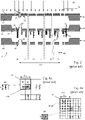
- FIG. 2 illustrates one suitable embodiment of a PD system 4, which comprises three plates stacked in a consecutive configuration: An "Aperture Array Plate” (AAP) 20, a “Deflection Array Plate” (DAP) 30 and a “Field-boundary Array Plate” (FAP) 40.
- AAP ture Array Plate
- DAP Deflect Array Plate
- FAP Field-boundary Array Plate
- 'plate' refers to an overall shape of the respective device, but does not necessarily indicate that a plate is realized as a single plate component even though the latter is usually the preferred way of implementation; still, in certain embodiments, a 'plate', such as the aperture array plate, may be composed of a number of sub-plates.
- the plates are preferably arranged parallel to each other, at mutual distances along the Z direction (vertical axis in Fig. 2 ).
- the flat upper surface of AAP 20 forms a defined potential interface to the charged-particle condenser optics/illumination system 3.
- the AAP may, e.g. be made from a square or rectangular piece of a silicon wafer (approx. 1mm thickness) 21 with a thinned center part 22.
- the plate may be covered by an electrically conductive protective layer 23 which will be particularly advantageous when using hydrogen or helium ions (line in US 6,858,118 ).
- the layer 23 may also be of silicon provided by the surface section of 21 and 22, respectively, so that there is no interface between layer 23 and the bulk parts 21, 22.
- the AAP 20 is provided with a plurality of apertures 24 formed by openings traversing the thinned part 22.
- the apertures 24 are arranged in a predetermined arrangement within an aperture area provided in the thinned part 22, thus forming an aperture array 26.
- the arrangement of the apertures in the aperture array 26 may be, for instance, a staggered arrangement or a regular rectangular or square array (cf. Fig. 4 ).
- the apertures 24 are realized having a straight profile fabricated into the layer 23 and a "retrograde" profile in the bulk layer of the AAP 20 such that the downward outlets 25 of the openings are wider than in the main part of the apertures 24.
- Both the straight and retrograde profiles can be fabricated with state-of-the-art structuring techniques such as reactive ion etching. The retrograde profile strongly reduces mirror charging effects of the beam passing through the opening.
- the DAP 30 is a plate provided with a plurality of openings 33, whose positions correspond to those of the apertures 24 in the AAP 20, and which are provided with electrodes 35, 38 configured for deflecting the individual beamlets passing through the openings 33 selectively from their respective paths.
- the DAP 30 can, for instance, be fabricated by post-processing a CMOS wafer with an ASIC circuitry.
- the DAP 30 is, for instance, made from a piece of a CMOS wafer having a square or rectangular shape and comprises a thicker part 31 forming a frame holding a center part 32 which has been thinned (but may be suitably thicker as compared to the thickness of 22).
- the aperture openings 33 in the center part 32 are wider compared to 24 (by approx.
- CMOS electronics 34 is provided to control the electrodes 35, 38, which are provided by means of MEMS techniques. Adjacent to each opening 33, a "ground" electrode 35 and a deflection electrode 38 are provided.
- the ground electrodes 35 are electrically interconnected, connected to a common ground potential, and comprise a retrograde part 36 to prevent charging and an isolation section 37 in order to prevent unwanted shortcuts to the CMOS circuitry.
- the ground electrodes 35 may also be connected to those parts of the CMOS circuitry 34 which are at the same potential as the silicon bulk portions 31 and 32.
- the deflection electrodes 38 are configured to be selectively applied an electrostatic potential; when such electrostatic potential is applied to an electrode 38, this will generate an electric field causing a deflection upon the corresponding beamlet, deflecting it off its nominal path.
- the electrodes 38 as well may have a retrograde section 39 in order to avoid charging.
- Each of the electrodes 38 is connected at its lower part to a respective contact site within the CMOS circuitry 34.
- the height of the ground electrodes 35 is higher than the height of the deflection electrodes 38 in order to suppress cross-talk effects between the beamlets.
- a PD system 4 with a DAP 30 shown in Fig. 2 is only one of several possibilities.
- the ground and deflection electrodes 35, 38 of the DAP may be oriented upstream (facing upward), rather than downstream.
- Further DAP configurations, e.g. with embedded ground and deflection electrodes, can be devised by the skilled person (see other patents in the name of the applicant, such as US 8,198,601 B2 ).
- the third plate 40 serving as FAP has a flat surface facing to the first lens part of the downstream demagnifying charged-particle projection optics 5 and thus provides a defined potential interface to the first lens 10a of the projection optics.
- the thicker part 41 of FAP 40 is a square or rectangular frame made from a part of a silicon wafer, with a thinned center section 42.
- the FAP 40 is provided with a plurality of openings 43 which correspond to the openings 24, 33 of the AAP 20 and DAP 30 but are wider as compared to the latter .
- the PD system 4, and in particular the first plate of it, the AAP 20, is illuminated by a broad charged particle beam 50 (herein, "broad" beam means that the beam is sufficiently wide to cover the entire area of the aperture array formed in the AAP), which is thus divided into many thousands of micrometer-sized beamlets 51 when transmitted through the apertures 24.
- the beamlets 51 will traverse the DAP and FAP unhindered.
- a deflection electrode 38 is powered through the CMOS electronics, an electric field will be generated between the deflection electrode and the corresponding ground electrode, leading to a small but sufficient deflection of the respective beamlet 52 passing through ( Fig. 2 ).
- the deflected beamlet can traverse the DAP and FAP unhindered as the openings 33 and 43, respectively, are made sufficiently wide. However, the deflected beamlet 52 is filtered out at the stopping plate 11 of the sub-column ( Fig. 1 ). Thus, only those beamlets which are unaffected by the DAP will reach the substrate.
- the reduction factor of the demagnifying charged-particle optics 5 is chosen suitably in view of the dimensions of the beamlets and their mutual distance in the PD device 4 and the desired dimensions of the structures at the target. This will allow for micrometer-sized beamlets at the PD system whereas nanometer-sized beamlets are projected onto the substrate.
- the ensemble of (unaffected) beamlets 51 as formed by AAP is projected to the substrate with a predefined reduction factor R of the projection charged-particle optics.
- a "beam array field” BAF
- BAF beam array field
- AX and AY denote the sizes of the aperture array field along the X and Y directions, respectively.
- the nominal width of a beamlet at the substrate i.e. aperture image
- the individual beamlets 51, 52 depicted in Fig. 2 represent a much larger number of beamlets, typically many thousands, arranged in a two-dimensional X-Y array.
- the applicant has realized such columns with a BAF of approx. 82 ⁇ m ⁇ 82 ⁇ m at the substrate.
- a pattern image pm as defined by the PD system 4 is produced on the target 16.
- the target surface covered with the charged-particle sensitive resist layer 17 will comprise one or more areas r1 to be exposed.
- the pattern image pm exposed on the target has a finite size y0 which is usually well smaller than the width of the area r1 which is to be patterned. Therefore, a scanning stripe exposure strategy is utilized, where the target is moved under the incident beam, so as to change the position of the beam on the target perpetually: the beam is effectively scanned over the target surface. It is emphasized that for the purpose of the invention only the relative motion of the pattern image pm on the target is relevant.
- the pattern image pm is moved over the area r1 so as to form a sequence of stripes s1, s2, s3, ... sn (exposure stripes), of width y0.
- the complete set of stripes covers the total area of the substrate surface.
- the scanning direction sd may be uniform or may alternate from one stripe to the next.
- the number of pixels of the standard image would be much higher.
- the number of pixels is only 180 for the better clarity.
- much more gray levels will be used within the scale from 0% to 100%.
- the pattern image pm ( Fig. 3 ) is composed of a plurality of pattern pixels px, which are exposed with dose values according to the desired pattern to be exposed. It should be appreciated, however, that only a subset of the pixels px can be exposed simultaneously since only a finite number of apertures is present in the aperture field of the PD system.
- the pattern of switched-on apertures is chosen according to the pattern to be exposed on the substrate.
- the exposure dose can vary from one pixel exposure cycle to the next whether the pixel is “switched on” or “switched off", depending on the pattern to be exposed or structured on the target.
- the same image element corresponding to a pattern pixel px on the target may be covered many times by the images of a sequence of apertures. Simultaneously, the pattern in the PD system is shifted, step by step, through the apertures of the PD system.
- a "white" shade corresponding to 100%.
- a gray shade may, for instance, be realized by switching on only a subset of apertures that may be involved in writing one pixel; for example, 4 out of 16 apertures would give a gray level of 25%.
- Another approach is reducing the duration of unblanked exposure for the apertures involved.
- the exposure duration of one aperture image is controlled by a gray scale code, for example an integer number.
- the exposed aperture image is the manifestation of one of a given numbers of gray shades that correspond to zero and the maximum exposure duration and dose level.
- the gray scale usually defines a set of gray values, for instance 0, 1/(n y -1) ..., i/(n y -1), ..., 1 with n y being the number of gray values and i an integer ("gray index", 0 ⁇ i ⁇ n y ). Generally, however, the gray values need not be equidistant and form a non-decreasing sequence between 0 and 1.
- Fig. 5 shows the arrangement of apertures in the aperture field of the PD device, according to a basic layout and also illustrates several quantities and abbreviations used in the following. Shown is the arrangement of the aperture images b1 as projected onto the target, shown in dark shades.
- the main axes X and Y correspond to the direction of advance of the target motion (scanning direction sd) and the perpendicular direction, respectively.
- Each aperture image has widths bX and bY along the directions X and Y respectively.
- the apertures are arranged along lines and rows having MX and MY apertures, respectively, with the offset between neighboring apertures in a line and row being NX and NY respectively.
- each aperture image belongs a conceptual cell C1 having an area of NX ⁇ bX ⁇ NY ⁇ bY, and the aperture arrangement contains MX.MY cells arranged in a rectangular way.
- these cells C1 are referred to as "exposure cells”.
- e The distance between two neighboring exposure positions.
- the distance e can be different from the nominal width b of an aperture image.
- e may be a fraction b/o of the width b of the aperture image, with o>1 being preferably (but not necessarily) an integer which we also refer to as the oversampling factor.
- the aperture images in the course of the various exposures, will spatially overlap, allowing a higher resolution of the placement of the pattern to be developed. It follows that each image of an aperture will, at one time, cover multiple pixels, namely o 2 pixels. The entire area of the aperture field as imaged to the target will comprise (NM o ) 2 pixels. From the point of view of placement of aperture image, this oversampling corresponds to a so-called placement grid which is different (since it is finer in spacing) than what would be necessary to simply cover the target area.
- a nominal location small square fields in Fig. 6B
- the offset to the previous nominal location (offset of the placement grid) is also of size b/2.
- the dose and/or the gray shade of each pixel may be adapted (reduced), by choosing suitable gray value for the aperture image that cover the respective pixel.
- an area of size a is printed but with an enhanced placement accuracy due to the finer placement grid.
- Direct comparison of Fig. 6B with Fig. 6A shows that locations of aperture images are just arranged on a placement grid twice (generally, o times) as fine as before, while the aperture images themselves overlap.
- the exposure cell C4 now contains (N o ) 2 locations (i.e., "pixels”) to be addressed during the write process and thus, by a factor of o 2 , more pixels than before.
- Fig. 7 shows an exposure scheme of the pixels, which is suitable for the invention. Shown is a sequence of frames, with increasing time from top (earlier) to bottom (later).
- the target moves continuously to the left, whereas the beam deflection is controlled with a seesaw function as shown on the left side of the figure.
- T1 the beam image stays fixed on a position on the target (corresponding to a position of a "placement grid").
- the beam image is shown to go through a placement grid sequence p11, p21, p31.
- the beamlets are moved over the distance of L G during the exposure of one set of image elements together with the target. In other words, all beamlets maintain a fixed position with regard to the surface of the substrate during the time interval T1.
- the beamlets are relocated instantaneously (within a very short time) to start the exposure of the image elements of the next placement grid.
- the exposure method may not produce a contiguous covering, so there may be a margin of length L that is not completely filled.
- the size of a single aperture image formed on the target is aX/R, where aX is the opening width of the apertures in the aperture array plate (AAP) and R is the reduction factor of the charged-particle projection optics.
- each exposure spot 60 corresponding to an aperture image bi0, bi1 ( Fig. 6A,B ) is exposed with discrete dose levels as will be discussed in more detail below.
- Figs. 8A-C illustrate various overlap configurations of special interest.
- Fig. 8A depicts the "Double Grid" multi-beam exposure as discussed above with Fig. 6B , where the overlap between the exposure spots is half of the beam spot size in X as well as in Y direction as shown in Fig. 8A .
- the physical grid size 61 is half of the linear size of the spots 60.
- the overlap between the spots is 1/4 of the beam spot size in X as well as in Y direction.
- the physical grid size 62 is a quarter of the spot size width.
- Fig. 8c depicts another grid layout, where in addition to Double Grid overlapping beam exposures, beam exposures are done in the centers in between. Therefore, the physical grid size 63 is 1/2 3/2 (i.e., ⁇ 2/4) of the linear spot size. This multi-beam exposure mode is called "Double-Centered Grid".
- Fig. 9 illustrates the exposure of one exposure spot with a maximum dose level.
- the maximum dose level is the sum of 15 dose level increments 64.
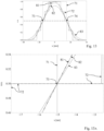
- Fig. 10 shows the ideal intensity profile 71 for a line of a width 30 nm, in the idealized case of zero blur.
- the overlap is a quarter of the beam size.
- the physical grid size is 5 nm.
- a discrete dose level can be assigned to each area of the physical grid, which is 5 nm ⁇ 5 nm for the example chosen; the line 72 in Fig.
- the blur 10 indicates the superposition of the intensity (or total dose) as it is composed by the overlapping exposure spots with discrete dose levels assigned to the pixel positions for generating the 30 nm line, whereas for better visibility the blur has been set to zero (so that the dose distribution of a single exposure spot becomes a rectangle).
- the blur has a realistic value such as shown in Fig. 13
- the step function at the edge of the rectangle is convoluted with a Gaussian function, which eventually transforms to a Gaussian shape. In that sense the line 72 can be seen as superposition of Gaussian functions at blur zero.
- the dose level histogram will not be symmetrical in order to position the left and right edge at predefined positions.
- Fig. 11 shows a simulation for a line of 30.0 nm width, with the left edge to be positioned at 0.0 nm and the right edge at 30.0 nm.
- the intensity profile 76 is formed by overlapping the profiles of the exposure spots 73, 74, and 75.
- the dose level of the leftmost exposure spot 74 is adjusted such that the 30 nm line starts at the desired start position 77, i.e. at 0 nm.
- the dose level of the rightmost exposure spot 75 is adjusted such that exposed line ends at position 78 at 30.0 nm.
- the overlap of the exposure spots 73, 74, 75 is a quarter of the beam size, i.e. 5 nm.
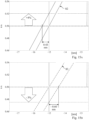
- Figs. 12A and 12B illustrate how the invention enables the MBW device to write lines with precise edge definitions; in each figure, the top frame shows the edge position error vs. line width, the middle frame the intensity profile, and the bottom frame shows the edge position deviation when enhancing the exposure dose by 10% vs. line width.
- Fig. 12A shows the intensity profile obtained for a 31.4 nm line width, and Fig. 12B for a 40.0 nm line width.
- the line width of the structure generated by the exposure can be changed in steps of 0.1 nm. Because of the integer dose levels there are slight deviations from the 0.1 nm address grid.
- edge position error top frames
- the change of edge position with 10% change of dose is only approx. 1 nm, varying only slightly with change of line width as shown in the bottom frames.
- the change of edge position with 1% change of dose is within approx. one atomic layer.
- Fig. 13 illustrates a most important advantage of the MBW, namely, that the line width is virtually independent of blur at the 50% dose threshold. Shown in Fig. 13 are the intensity profile 71 for zero blur, the dose level histogram 72, and resulting intensity profiles 81, 82, 83 calculated with 3.5 nm, 5.0 nm, and 7.5 nm 1sigma blur, respectively.
- the edge positions 73 and 74 of the generated structure are where the zero blur intensity profile 71 crosses the "0.5" intensity level.
- the enlarged detail of Fig. 13A shows the region around the position 73 at the left-side flank.
- the dose level assignments 72 are for using 20 nm beam size with 1sigma blur of 5 nm and Quad Grid multi-beam exposure, providing a 5 nm physical grid size.
- Figs. 14A, 14B, and 14c show intensity profile diagrams illustrating how the multi-beam exposure methods illustrated here can achieve a fine positioning of structure feature with resolution smaller than the grid size.
- the discrete dose levels are visualized as rectangles 64 of uniform height, piled up in a "brick-layer” arrangement; of course, this "brick-layer" depiction is only symbolical and intended to facilitate interpretation of the drawings.
- Fig. 14A shows a dose level histogram, for the example of a line of 30nm width exposed by means of a 4bit (i.e., 15 dose levels per spot) exposure in a Quad Grid with a beam spot size of 20nm width.
- the grid size 62 is 1/4 of the linear size of the exposure spots, which are symbolized as rectangles piled up in a "brick-layer" arrangement, and the resulting dose level distribution 65 is outlined as a bold line.
- the line width can be made smaller or larger in very fine steps, which are smaller than the grid size, in this case the Quad Grid size 62. Reducing the line width can be achieved by lowering the dose level of the outermost exposure spots and/or omitting exposure spots (the latter when the reduction is at least about one half of a exposure spot size). Increasing the line width can be achieved by enhancing the dose level of the outermost exposure spots and/or, in particular when the maximum dose level has been reached, to add an additional, preferably overlapping, exposure spot. The latter aspect is illustrated in Fig. 14A : an exposure spot 66 having a defined dose level is added, resulting in a dose level histogram 67 for the line with larger width compared to 65.
- Fig. 14B illustrates a shift of the line without changing the width, which is achieved by removing dose levels from spot 68 and adding dose levels from spot 69, resulting in the dose level histogram 70 which corresponds to a line shifted to the right as compared to the line of Fig. 14A .
- Figs. 14A-C The intensity profiles of Figs. 14A-C are shown along the X direction of the target plane. It is straightforward to extend the multi-beam exposure methods illustrated here to lines along other directions as well, and fine positioning can be achieved for lines at any angle to the on the target plane.
- a dose error causing a dose level decrement of -5% will shift the edge position by -0.60 nm, so instead of a CD of 30.0 nm, a line with 28.8 nm width would be printed.
- a correction of CD is proposed which can be done by a convolution of the graphical representation of the desired pattern, such as rasterized bitmap data, with a matching convolution kernel (MCK), short "kernel”.
- MCM convolution kernel
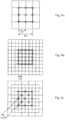
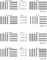
- Figs. 16A-H Simple examples of kernels according to the invention are shown in Figs. 16A-H .
- the left-hand portion represents an original pattern
- a 3 ⁇ 3 kernel is shown
- the right-hand portion shows the resulting pattern when the respective kernel is applied.
- kernel M3A a widening of vertical and horizontal lines is accomplished, as illustrated in Fig. 16A.
- Fig. 16B illustrates the opposite case where kernel M3B effectuates a reduction of the width of the vertical and horizontal lines.
- This is achieved by unnormalized kernels M3A, M3B, i.e. kernels where the normalization K o ⁇ K kl (i.e., the sum over all elements) is different from 1.
- the normalization is greater than one, K o > 1; whereas for kernel M3B the normalization is smaller than one, K o ⁇ 1.
- FIG. 16F-H Further examples relating to the invention are illustrated in Figs. 16F-H.
- Fig.16F shows a variant which leads to a broadening of lines in all direction using a simple kernel M3F with only one central entry larger than one (unnormalized kernel). This corresponds to an increment of the overall dose via a convolution.
- the opposite case is illustrated in Fig.16c using a simple kernel M3G which only has one central entry, but smaller than one.
- Fig.16H where a single non-zero entry (normalized) located off the center of the kernel M3H leads to a shift of the whole pattern.
- the various examples given here may be combined or modified as deemed suitable for a specific application.
- FIG. 17 shows the widening of the 30 nm line with the dose level histogram 65 ( Fig. 14A ) by adding overlapping exposure spots 84 and 85 to result in the dose level histogram 86.
- a further aspect of the invention envisages the application of different kernels in different areas of a beam array field (BAF).
- BAF beam array field
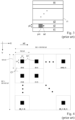
- a suitable way to determine the various kernels M11...Mmn is by printing a particular test pattern (typically lines and spaces in different directions, e.g. in horizontal, vertical, 45° and 135° orientation, having specific nominal CDs) within a beam array field, i.e. local, and carefully measuring the ⁇ CD values in in the respective directions (X, Y, 45° and 135°) in the m ⁇ n subfields, e.g. using a suitable scanning electron microscope (so called CD-SEM).
- CD-SEM scanning electron microscope
- a corresponding subfield-kernel ( Fig. 18B ) is generated for compensating the ⁇ CD values.
- a further MBW exposure is done which is evaluated to result in improved ⁇ CDX* and ⁇ CDY* values ( Fig. 18c ).
- an improved set of kernels to replace the kernels MCK-BAF_11 ... MCK_BAFMn, may be determined; this may be iterated as often as suitable.
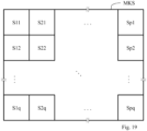
- Fig. 19 illustrates another approach using multiple kernels, namely, with regard to the substrate exposure field (SEF, denoted MKS in Fig. 19 ), i.e., the image area on the target which is to be exposed, that is, the global field.
- SEF substrate exposure field
- MKS substrate exposure field
- this approach envisages to divide the SEF into a discrete number of subfields, e.g. p ⁇ q subfields S11, S21, ... Sp1, S12 ... Spq and to assign a MCK to each of these subfield.
- FIG. 20A to 20c which are depictions analogous to Figs.18A-C , after MBW exposure and having measured the ⁇ CDX, ⁇ CDY, ⁇ CD_45° and/or ⁇ CD_135° in each of these subfields SEF_11...SEF_pq, e.g. using a CD-SEM ( Fig. 20A ), the kernels MCK-SEF_11 ... MCK_SEFpq for each of the subfields ( Fig. 20B ) are applied to expose a second substrate exposure field, so that the improved values ⁇ CD* and ⁇ CD* can be obtained ( Fig. 20c ).
- an improved set of kernels to replace the kernels MCK-SEF_11 ... MCK_SEFpq, may be constructed for a further optional exposure of the test patterns distributed on the SEF, with respect to subfields, which should then yield a further adapted/improved GCDU. This can be iterated as often as suitable.
- the method is exemplified to a case of strongly degraded intensity blur.
- a situation might be the case when using a chemically amplified resist (CAR) materials with very low (5-10 ⁇ C/cm 2 ) exposure dose.
- CAR chemically amplified resist
- Such low dose CAR materials exhibit strong side diffusion and therefore cause a significant degradation of intensity blur.
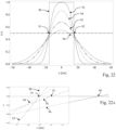
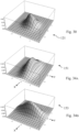
- Fig. 21 shows an example where the point spread function (PSF) 87 with 5 nm 1sigma blur of a MBW electron-optical column is degraded to a PSF 88 with 20 nm 1sigma blur.
- PSF point spread function
- the intensity profile 90 is shown for a line with 30 nm line width.
- the "0.5" level of the intensity profile corresponds to the "dose to clear” separating regions with and without resist development from each other. Since the "0.5" level defines the edge of the line to be written, the effect of the blur may cause different dose latitudes and thus deviations of the edge position as written from the nominal desired positions.
- the desired positions 91 and 92 of the left-hand edge and right-hand edge, respectively, are met for the zero-blur intensity profile 90.
- the intensity profile 93 can still fulfill this condition to a large extent; but the intensity profiles 94, 95, and 92, which correspond to 10 nm, 15 nm, and 20 nm 1sigma blur, respectively, are increasingly deviating.
- the positions of the intensity-profile i.e., "0.5"-level intersections
- desired edge positions 91 and 92 left-hand and right-hand edge, respectively
- degraded edge positions 97 and 98 respectively
- a homogenization of the beam blur with the MBW BAF is accomplished according to the invention by a convolution of the graphical representation of the desired pattern, such as rasterized bitmap data, with a MCK kernel.
- This kernel according to the invention enables to eventually generate virtually the same intensity distribution over the BAF.
- Fig. 23 shows an example of a kernel 89 according to the invention, in this case for having a MBW with 20 nm beam size and Quad grid exposure (5nm physical grid size) emulate a "deteriorated"region within the beam array field having a 1sigma blur of 20 nm.
- the kernel is shown in a histogram representation 89', equivalent to a representation as a one-dimensional array of rounded real values. The methods how to determine the kernel are explained below.
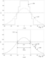
- the kernel may also have a simple shape, such as a rectangle shape (i.e., taking a constant value within finite interval, but zero elsewhere; that is, a rectangular function, see Fig.
- the kernel functions of Figs. 24A-D are characterized by a spatial range parameter (width of rectangle or triangle, distance of first zero from the maximum, or FWHM parameter of the Gaussian) which is typically chosen corresponding to the blur value of the reference tool. For example in Fig.
- the full range of the blur would be in the order of twice the full-width-half-maximum value of the blur when this kernel is used to match the blurring behavior of the reference tool.
- the spatial distance between the first-order zeros is a measure of the dose slope that is generated by filtering, or in special cases causes a selectivity for features that correlate with this length.
- the kernel in Fig. 24c allows to pronounce features with size 30 nm, which is the approximate distance of the first-order zeros.
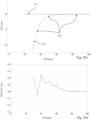
- Fig. 27 shows the dose level convolution 106 which is obtained by convoluting the kernel 89 ( Fig. 23 ) with the MBW dose level assignment 65 ( Fig. 14A ) for a line width of 30 nm.
- an intensity profile as indicated by symbols 104 is obtained as shown in Fig. 26 .
- the dotted line 105 represents the intensity profile 96 with 20 nm 1sigma blur ( Fig. 21 ). It is important to note that the two intensity profiles 104 and 105 coincide with only minimal deviation, barely visible in Fig. 26. Fig. 26 also illustrates the zero blur intensity profile 71 of the 30 nm line.
- the MBW tool exposure was "degraded" with the convolution kernel in a manner which exactly matches the behavior when having a PSF intensity blur 88 with 20 nm 1sigma blur.
- the same kernel 89 was used to generate a dose level convolution 107, leading to an intensity profile 108, which is virtually coinciding with the intensity profile 109 when having a PSF intensity blur 88 with 20 nm 1sigma blur.
- the line 110 indicates the target line of 40 nm.
- the curve 111 illustrates the relationship for the MBW, in this case for a Quad Grid exposure with 20 nm beam spots with 1sigma blur of 5 nm: there is virtually no deviation, i.e. we have a flat relationship 111.
- the deviations of the curve 111 from an ideal horizontal line are ⁇ ⁇ 0.1 nm, corresponding to twice the maximum edge position errors of ⁇ 0.05 nm as shown in the upper part of Fig. 12B .
- Fig. 29A the MBW convoluted with the kernel 89 results in a performance 113 which is virtually the same as 112.
- Fig. 29B shows in detail the difference between the values of curves 113 and 112 of ⁇ CD as function of CD.
- the deviations are smaller than 0.25 nm for CD values equal or above 30 nm.
- the method according to the invention can emulate MBW tool exposures with large blur to a very good degree with only very small deviations from the significant parameters such as CD.
- the deviations could be further reduced by (i) further suitable optimizing the kernel, (ii) using smaller beam size with the MBW, or (iii) using a smaller physical grid on the target in the MBW.
- an isotropic kernel 121 as illustrated in Fig. 30 may be used.
- the kernel 121 was generated by rotating the kernel 89 ( Fig. 23 ).
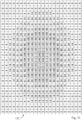
- the kernel 121 may be represented also in the form of a matrix of (e.g., integer or real) values.
- the kernel 121 has size of 22 ⁇ 22, but it is expected that for most implementations smaller kernels, such as of sizes 5 ⁇ 5, 7 ⁇ 7 or 11 ⁇ 11, will be sufficient to meet processing requirements; but of course larger kernels may be suitable as well.
- the kernel is determined prior to any pattern calculation, and is then applied to the pixel data.
- the calculation is performed by a convolution so as to obtain the pixel data for the MBW matched to the reference tool.
- Figs. 32A-C illustrate a simplified example for a kernel of size 5 ⁇ 5 ( Fig. 32B ).
- the kernel is applied to the pixel data; only those pixels in Fig. 32A are specified by symbols P i + k,j + l which are used in the convolution calculation according to formula (1) above (in this case the offset indices k and j in the sum independently run through values -2, ... +2).
- Fig. 33A-C show three 2D simulations for a line having 30 nm width; half of the line is shown only, as the other half is the symmetrical image. Shown are contour plots for 45%, 50%, and 55% dose level with regard to the maximum dose; the dotted rectangle indicates the target shape of the 30 nm line.
- Fig. 33A illustrates the result of simulations for a line 300 nm long when using the MBW with beam size of 20 nm with a 1sigma blur of 5 nm and Quad Grid exposure (i.e., 5 nm physical grid size). The 50% dose level is the resist contour obtained with development (assuming high resist contrast).
- Fig. 33B shows the result of corresponding simulations for the reference tool, e.g.
- Fig. 33c illustrates the result for (simulated) exposure with the MBW convoluted with the kernel 121 of Fig. 30 with the target to match the 30nm line as exposed with reference tool line. The excellent match with the profile of Fig. 33B is evident.
- a kernel as described in the present disclosure need not be isotropic within the XY plane.
- a MBW machine has written a mask and careful metrology analysis reveals that on the mask the width of lines in X direction are different from the width of comparable lines in Y direction to a certain extent; in order to emulate such a situation, not forming part of the present invention, in another MBW device, one suitable approach is to employ an anisotropic kernel. Examples of anisotropic kernels are shown in Figs. 34A and Fig. 34B . In particular, Fig.
- FIG. 34A illustrates an anisotropic kernel 151 with a large line width along the X direction, about doubled of the line width along the Y direction; in contrast, the kernel 153 depicted in Fig. 34B has an anisotropy with the larger line width along the Y direction.
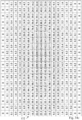
- Fig. 34C illustrates a matrix representation 152 of the kernel 151 of Fig. 34A , where, for instance, the individual values (not normalized) are given as real values rounded to one decimal digit.
- kernels are not restricted to lines in X or Y directions but may be applied also to anisotropies oriented at an arbitrary angle to X / Y direction.
- an anisotropic kernel also offers a way to compensate a known anisotropy
- reference tool of other type for instance an anisotropy towards the X direction could be compensated using a kernel anisotropic towards the Y direction, or vice versa (or with regard to arbitrary perpendicular axes).
- kernels are of illustrative purpose only; further implementations of kernels and application to other tasks of considerable importance will be obvious for the skilled person.
- One of the many possible variants of a kernel includes time-dependent values.
- the time-dependency may comprise a function corresponding to a fluctuation function of the total current emitted from the source, which has been experimentally determined prior to the calculation process.
- multiple kernels may be used within one writing process. For instance, different kernels may be used for different areas of the target. This is advantageous in cases, not covered by the present invention, where, for instance, the reference tool exhibits varying imaging behavior over the areas on the target to be exposed, such as a non-uniform anisotropy.
- the beam size might be changed during the writing process, e.g., from 20 nm to 10 nm, for instance by switching between different aperture arrays within the PD device (see US 8,546,767 ). In this case, a first kernel is used for the exposure with 20 nm beam size, and a second kernel is used with the 10 nm beam size.
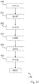
- Fig. 35 shows a flowchart of the datapath 170 in the context of the invention.
- the data path is preferably performed in the processing system 18 of the writer tool ( Fig. 1 ) in real time; in a variant, part or all of the calculations of the data path may be performed in advance, for instance in a suitable computer.
- the complete pattern image comprises a vast amount of image data, which is why for efficient computation of those data a high-speed datapath that generates the pixel data to be exposed, preferably in real-time, will be suitable.
- the pattern to be exposed is typically described in a vector format, e.g. as a collection of geometries like rectangles, trapezoids or general polygons, which typically offers better data compaction and therefore reduces the requirements on data storage.
- the datapath therefore consists of three major parts:
- the datapath starts upon being supplied a pattern PDATA to be exposed at step 160.
- the pattern data may have already been modified in a previous step (not shown) in order to correct for a specific writing behavior, as for example the line end shortening as shown in Fig. 33B .
- the pattern PDATA to be exposed is split into a large number of small data chunks, possibly with geometric overlaps. Corrections that can be applied in the vector domain (e.g. proximity effect correction) may be carried out to all chunks independently, possibly in parallel, and the resulting data is sorted and coded in a way to improve computation speed of the following steps.
- the output is a collection of chunks where all chunks contain a collection of geometries.
- Stage 161 Rasterization RAST.
- the geometries of every chunk are converted into a raster graphics array, where the pixel gray level represents the physical dose of the corresponding aperture image. Every pixel that is completely inside a geometry is assigned the color of the polygon, whereas the color of pixels that cross an edge of a geometry is weighed by the fraction of the area of the pixel that is covered by the geometry. This method implies a linear relation between the area of the geometry and the total dose after the rasterization.
- the doses are first calculated as floating point numbers; only later they are converted to the discrete set of dose values as supported by the PD device. As a result of rasterization the pixel data will be in the format of floating point numbers representing nominal dose values P for the respective pixels.
- Stage 162 Kernel matching KERM.
- a pre-determined MCK kernel is applied to the pixel data. This is done by a convoluting the pixel data with the kernels described above. Preferably, in order to achieve real-time processing speed, a sufficient number of parallel CPUs and GPUs are used. Since the convolution kernel typically acts on the range of the blur, which is a few tens on nanometers, it is possible to parallelize the calculation processes in an effective way where the pixel data of the beam array are distributed over different CPUs and/or GPUs.
- Stage 163 Other pixel based corrections CORR, such as compensation of deviations from a uniform current density of the beam 50 over the aperture field, and/or correction for individual defective beam deflectors in the DAP 30. Correction methods of this kind do not form part of the invention and are not discussed here.
- Stage 164 Dithering DITH.
- the dithering process converts the convoluted, and possibly corrected, dose value data P° into gray value data, based on a predetermined gray value scale. This is a position-dependent rounding process that ensures that rounding errors are averaged over nearby pixels which, combined with oversampling, allows for a much finer dose variation than with the discrete set of dose values available for a single aperture; it can be realized by means of known algorithms for the conversion of visual image data into pixel graphics. It is possible to apply additional corrections (which are not part of the present invention) at this stage, provided they can be applied in the pixel domain, immediately before or after dithering depending on the actual correction (e.g. defective apertures correction).
- Stage 165 Pixel packaging, PPACK.
- the pixel image obtained from stage 164 is sorted according to the placement grid sequence and sent to a pixel buffer PBUF which is provided in the processing system 18 of the writer tool ( Fig. 1 ).
- the pixel data is buffered until a sufficient amount of data, typically at least the length of a stripe, is present which triggers the exposure of the stripe (see Fig. 7 ).
- the data is taken out of the buffer during the writing process. After the stripe has been written, the process described above starts anew for the pattern data of the next region, such as the next stripe.
- the intensity profile of the reference tool for instance the intensity profile 87, 88 of a VSB writer ( Fig. 21 ), is known; for instance it has been determined experimentally.
- linearity plots Fig. 29A
- an experimental set of data for example, a set of line widths as function of varying dose or varying design width, printed by the reference tool may be taken as initial data to determine the intensity profile.
- the intensity profiles are known (mathematically, the point spreading function, which is the dose distribution that an indefinitely small pattern element, like for example a delta function, generates on the substrate during the exposure, including blurring and other imaging artifacts).
- the determination and optimization of the MCK is typically an iterative process, where a certain number of points representing the MCK kernel is varied systematically and/or stochastically so as to be optimized with respect to a target function (figure of merit).
- the target function can, for example, be the integral of the difference in linearity function (cf. Fig 29B ) or, in case of optimizing directional line width variation as discussed with reference to Figs. 34A and 34B , the difference between the line widths for the line directions of interest.
- a target function can, for example, be the integral of the difference in linearity function (cf. Fig 29B ) or, in case of optimizing directional line width variation as discussed with reference to Figs. 34A and 34B , the difference between the line widths for the line directions of interest.
- a gradient method or a linear regress method.
- the intensity profile of the reference tool shown as an example in Fig. 24D in form of a single Gaussian function, is used.
- the intensity profile already presents a suitably good approximation for the final kernel, and further optimization is only needed in order to comply with higher demands in accuracy of the matching.
- Figs. 24A-D show examples of kernel functions that are suitable as starting functions for the linear regress calculation to find the optimum kernel. Alternatively, they may be sufficient for a number of tasks directly (without subsequent optimization).
- a rectangle function as depicted in Fig. 24A can also be used to achieve certain purposes as for example "moving averaging”
- the triangle function of Fig. 24B is suitable for performing a weighted averaging
- a sinc function as depicted in Fig. 24c may be used to obtain an "edge enhancement" or "patterns selective" filtering, where the kernel has the effect of a differentiation
- Fig. 24D illustrates a Gaussian shape.
- the negative values of the sinc-shaped kernel may result in nominal negative doses, to be replaced by a non-negative cut-off value such as zero, in order to avoid negative dose values on the substrate.
- the MBW will itself have a blur (due to width of a spot and the point spread function).
- the MBW blur is usually very small as compared to the line width to be written on the target (by a factor of at least 1.5, typically 3 or even more), and even more so as compared the blur of the reference tool; therefore the MBW blur can be neglected for determining the kernel without significant detriment at least at the first stage. In the iterative approach, this is a safe procedure since the iteration will implicitly take into account effects of the MBW blur. In fact, it was found that usually the deviations introduced by neglecting the MBW blur in the kernel are marginal only already at the first stage.
Landscapes
- Engineering & Computer Science (AREA)
- Chemical & Material Sciences (AREA)
- Analytical Chemistry (AREA)
- Computer Hardware Design (AREA)
- Physics & Mathematics (AREA)
- Theoretical Computer Science (AREA)
- Evolutionary Computation (AREA)
- Geometry (AREA)
- General Engineering & Computer Science (AREA)
- General Physics & Mathematics (AREA)
- Architecture (AREA)
- Electron Beam Exposure (AREA)
Claims (13)
- Verfahren zum Berechnen eines Belichtungsmusters für die Belichtung eines gewünschten Musters auf einem Target (16) in einer Einrichtung zur Multistrahl-Bearbeitung (1) mit geladenen Teilchen, in der ein Teilchenstrahl (lb, 50) auf eine Musterdefinitionsvorrichtung (4) gerichtet wird und diese beleuchtet, welche Musterdefinitionsvorrichtung eine Aperturenarray (26) aufweist, das aus einer Vielzahl von Blanking-Aperturen (24, 33, 43) besteht, durch die der Teilchenstrahl (pb) zum Schreiben des gewünschten Musters durch Belichten einer Vielheit von Pixels (px) innerhalb eines Bildbereichs auf dem Target hindurchtritt,wobei in der Musterdefinitionsvorrichtung die Vielzahl von Blanking-Aperturen (24, 33, 43) sich in einer vorbestimmten Anordnung befinden, die die Positionen der Blanking-Aperturen zueinander festlegt, wobei jede Blanking-Apertur selektiv hinsichtlich eines Dosiswerts einstellbar ist, der durch die jeweilige Blanking-Apertur auf ein entsprechendes, auf dem Target während einer jeweiligen Belichtungsdauer erzeugtes Aperturenbild eingestrahlt werden soll, wobei der Dosiswert jeweils einen aus einer diskreten Grauskala ausgewählten Wert annimmt,wobei während eines Schreibprozesses für das gewünschte Muster eine Abfolge von Belichtungsdauern (T1) stattfindet, wobei in jeder Belichtungsdauer die Blanking-Aperturen auf das Target (16) abgebildet werden und so eine entsprechende Vielzahl von Aperturenbildern (b1, bi0, bi1) erzeugen, um Pixel in Übereinstimmung mit dem gewünschten Muster zu belichten,wobei das Verfahren umfasst:wobei der Faltungs-Kernel dazu eingerichtet ist, eine kritische Dimension entlang zumindest einer Richtung im Bildbereich auf dem Target einzustellen, zum Kompensieren einer Abweichung der Abbildung von der Musterdefinitionsvorrichtung (4) zum Target (16), wobei der Faltungs-Kernel dazu eingerichtet ist, eine Punktverbreiterungsfunktion der Abbildung verschlechtert, um eine Intensitätsverteilung in einem spezifischen Gebiet innerhalb des Strahl-Arraybereichs mit einer vergrößerten Unschärfe zu emulieren.i) Bereitstellen des gewünschten Musters als grafische Darstellung (72, 106) auf dem Bildbereich auf dem Target, wobei die grafische Darstellung (72, 106) eine vorbestimmte Auflösungsbreite hat, die größer ist als ein nomineller Abstand zwischen benachbarten Positionen der Pixel in dem Bildbereich,ii) Bereitstellen eines Faltungs-Kernels (89', 121), welcher eine Abbildung von einem Element der graphischen Darstellung auf eine Gruppe von Pixels beschreibt, wobei die Gruppe von Pixels um eine nominelle Position des Elements zentriert ist, undiii) Berechnen eines nominellen Belichtungsmusters als eine auf der Vielheit von Pixels definierte Pixel-Rastergrafik (ps), durch Faltung der grafischen Darstellung (72, 106) mit dem Faltungs-Kernel (89', 121), wobei sich durch das nominelle Belichtungsmuster eine nominelle Dosisverteilung auf dem Target erzeugen lässt,
- Verfahren nach Anspruch 1, wobei der Schreibprozess Aperturenbilder erzeugt, die sich gegenseitig überlappen, und die Aperturenbilder eine nominelle Breite (b) aufweisen, die ein Vielfaches des Abstands (e) zwischen Pixelpositionen benachbarter Aperturenbilder ist, die auf dem Target erzeugt werden, wobei das Verfahren den zusätzlichen Schritt aufweist:
iv) Erzeugen eines Belichtungsmusters, das zum Belichten des gewünschten Musters durch den Schreibprozess durch Belichtung von Aperturenbildern geeignet ist, aus dem nominellen Belichtungsmuster. - Verfahren nach Anspruch 1 oder 2, wobei in Schritt i die grafische Darstellung (72, 106) eine Rastergrafik auf einem Referenzraster mit einer Rasterbreite ist, wobei die Rasterbreite als Auflösungsbreite verwendet wird.
- Verfahren nach Anspruch 1 oder 2, wobei in Schritt i die grafische Darstellung (160) eine Vektorgrafik ist, die in eine Rastergrafik auf einem Referenzraster umgewandelt wird mit einer Rasterbreite, die vorzugsweise größer ist als ein nomineller Abstand zwischen benachbarten Positionen der Pixel innerhalb des Bildbereichs.
- Verfahren nach einem der vorhergehenden Ansprüche, wobei die Berechnungen von Schritt iii und, falls vorhanden, nachfolgender Berechnungen während eines Schreibprozesses in Echtzeit durchgeführt werden, wobei zugehörende Berechnungen transient ohne dauerhafte Speicherung der berechneten Daten durchgeführt werden.
- Verfahren nach einem der vorhergehenden Ansprüche, wobei der Faltungs-Kernel (121, 151, 153) als eine diskrete Matrix (122, 152) von Pixelwerten dargestellt ist und die Faltung in Schritt iii als diskrete Faltung durchgeführt wird.
- Verfahren nach einem der vorhergehenden Ansprüche, wobei der Faltungs-Kernel zeitabhängige Werte enthält, die eine Zeitabhängigkeit (f(t)) entsprechend einem zeitabhängigen Schreibverhalten einer zu emulierenden Referenz-Schreibeinrichtung haben.
- Verfahren nach einem der vorhergehenden Ansprüche, wobei der Faltungs-Kernel (151, 153) anisotrop in Bezug auf kritische Dimensionen entlang der beiden Hauptrichtungen auf dem Bildbereich ist, wie sie bei der Abbildung der Blanking-Aperturen auf das Target (16) erzeugt werden.
- Verfahren nach einem der vorhergehenden Ansprüche, wobei auf der Grundlage einer vordefinierten Aufteilung der Fläche des Aperturfeldes in eine Vielzahl von Teilbereichen zwei oder mehr unterschiedliche Faltungs-Kernels (M11, ..., Mmn) verwendet werden, wobei jeder Teilbereich aus der Vielzahl von Teilbereichen einem der Kernels zugeordnet ist, der in dem jeweiligen Teilbereich verwendet wird.
- Verfahren nach einem der vorhergehenden Ansprüche, wobei die Faltung in Schritt iii unter Verwendung arithmetischer Werten durchgeführt wird, die eine höhere arithmetische Genauigkeit als die Auflösung der diskreten Grauskala haben.
- Verfahren nach einem der vorhergehenden Ansprüche, wobei zwei oder mehr Faltungs-Kernels verwendet werden, wobei jeder Kernel auf einen jeweiligen Teilbereich aus einer Vielzahl von Teilbereichen (S11, ..., Spq) innerhalb des Bildbereichs und/oder mit einem jeweiligen Aperturenarray aus einer Vielzahl von Aperturenarrays, die der Musterdefinitionsvorrichtung zugeordnet sind, verwendet wird.
- Verfahren nach einem der vorhergehenden Ansprüche, wobei während des Schreibprozesses die Position der Aperturenbilder während einer Belichtungsdauer relativ zum Target an der Position eines Pixels (px) fixiert bleibt, aber zwischen den Belichtungsdauern die Position der Aperturenbilder über das Target verschoben wird, und so die Vielzahl der Pixel innerhalb des Bildbereichs auf dem Target belichtet wird.
- Verfahren nach einem der vorhergehenden Ansprüche, wobei die Auflösungsbreite der grafischen Darstellung (72, 106) größer ist als eine nominelle Breite der Aperturenbilder, die von der Einrichtung zur Multistrahl-Bearbeitung (1) mit geladenen Teilchen erzeugt werden.
Priority Applications (1)
| Application Number | Priority Date | Filing Date | Title |
|---|---|---|---|
| EP15175372.0A EP2927748B1 (de) | 2014-07-10 | 2015-07-06 | Kompensation von bildabweichungen in einem partikelstrahlschreiber unter verwendung eines faltungskerns |
Applications Claiming Priority (3)
| Application Number | Priority Date | Filing Date | Title |
|---|---|---|---|
| EP14176563 | 2014-07-10 | ||
| EP14199183 | 2014-12-19 | ||
| EP15175372.0A EP2927748B1 (de) | 2014-07-10 | 2015-07-06 | Kompensation von bildabweichungen in einem partikelstrahlschreiber unter verwendung eines faltungskerns |
Publications (3)
| Publication Number | Publication Date |
|---|---|
| EP2927748A2 EP2927748A2 (de) | 2015-10-07 |
| EP2927748A3 EP2927748A3 (de) | 2015-12-30 |
| EP2927748B1 true EP2927748B1 (de) | 2023-03-01 |
Family
ID=53491459
Family Applications (2)
| Application Number | Title | Priority Date | Filing Date |
|---|---|---|---|
| EP15175373.8A Active EP2966504B1 (de) | 2014-07-10 | 2015-07-06 | Anpassung eines partikelstrahlschreibers mithilfe eines faltungskerns |
| EP15175372.0A Active EP2927748B1 (de) | 2014-07-10 | 2015-07-06 | Kompensation von bildabweichungen in einem partikelstrahlschreiber unter verwendung eines faltungskerns |
Family Applications Before (1)
| Application Number | Title | Priority Date | Filing Date |
|---|---|---|---|
| EP15175373.8A Active EP2966504B1 (de) | 2014-07-10 | 2015-07-06 | Anpassung eines partikelstrahlschreibers mithilfe eines faltungskerns |
Country Status (4)
| Country | Link |
|---|---|
| US (2) | US9373482B2 (de) |
| EP (2) | EP2966504B1 (de) |
| JP (2) | JP6892214B2 (de) |
| KR (2) | KR102357185B1 (de) |
Families Citing this family (33)
| Publication number | Priority date | Publication date | Assignee | Title |
|---|---|---|---|---|
| EP2937889B1 (de) | 2014-04-25 | 2017-02-15 | IMS Nanofabrication AG | Mehrstrahliges werkzeug zum schneiden von mustern |
| EP3358599B1 (de) | 2014-05-30 | 2021-01-27 | IMS Nanofabrication GmbH | Kompensation von dosisinhomogenität mittels zeilenkalibrierung |
| JP6892214B2 (ja) | 2014-07-10 | 2021-06-23 | アイエムエス ナノファブリケーション ゲーエムベーハー | 畳み込みカーネルを使用する粒子ビーム描画機のカスタマイズ化 |
| US9568907B2 (en) | 2014-09-05 | 2017-02-14 | Ims Nanofabrication Ag | Correction of short-range dislocations in a multi-beam writer |
| JP5816739B1 (ja) * | 2014-12-02 | 2015-11-18 | 株式会社ニューフレアテクノロジー | マルチビームのブランキングアパーチャアレイ装置、及びマルチビームのブランキングアパーチャアレイ装置の製造方法 |
| US9658538B2 (en) * | 2014-12-19 | 2017-05-23 | Taiwan Semiconductor Manufacturing Company, Ltd. | System and technique for rasterizing circuit layout data |
| US9653263B2 (en) | 2015-03-17 | 2017-05-16 | Ims Nanofabrication Ag | Multi-beam writing of pattern areas of relaxed critical dimension |
| EP3096342B1 (de) | 2015-03-18 | 2017-09-20 | IMS Nanofabrication AG | Bidirektionales mehrstrahliges schreiben mit doppeldurchgang |
| US10410831B2 (en) | 2015-05-12 | 2019-09-10 | Ims Nanofabrication Gmbh | Multi-beam writing using inclined exposure stripes |
| JP6590542B2 (ja) * | 2015-06-15 | 2019-10-16 | 株式会社ニューフレアテクノロジー | 荷電粒子ビーム描画方法及び荷電粒子ビーム描画装置 |
| JP6727021B2 (ja) * | 2016-04-26 | 2020-07-22 | 株式会社ニューフレアテクノロジー | マルチ荷電粒子ビーム照射装置、マルチ荷電粒子ビームの照射方法及びマルチ荷電粒子ビームの調整方法 |
| EP3258479B1 (de) * | 2016-06-13 | 2019-05-15 | IMS Nanofabrication GmbH | Verfahren zur kompensation von durch variation von musterbelichtungsdichte verursachten musterplatzierungsfehlern in einem mehrstrahlenschreiber |
| US10325756B2 (en) | 2016-06-13 | 2019-06-18 | Ims Nanofabrication Gmbh | Method for compensating pattern placement errors caused by variation of pattern exposure density in a multi-beam writer |
| JP6858243B2 (ja) * | 2016-07-25 | 2021-04-14 | シーメンス・ヘルスケア・ダイアグノスティックス・インコーポレーテッドSiemens Healthcare Diagnostics Inc. | 試料容器の容器キャップを識別するためのシステム、方法及び装置 |
| JP6881168B2 (ja) * | 2016-09-29 | 2021-06-02 | 大日本印刷株式会社 | マルチビーム電子線描画装置における露光強度分布を求める方法および装置 |
| WO2018061960A1 (ja) * | 2016-09-29 | 2018-04-05 | 大日本印刷株式会社 | マルチビーム電子線描画装置における露光強度分布を求める方法および装置 |
| WO2018121967A1 (en) * | 2016-12-28 | 2018-07-05 | Asml Netherlands B.V. | Methods of determining scattering of radiation by structures of finite thicknesses on a patterning device |
| EP3355337B8 (de) * | 2017-01-27 | 2024-04-10 | IMS Nanofabrication GmbH | Erweiterte quantisierung auf dosisebene für mehrstrahlschreiber |
| US10325757B2 (en) | 2017-01-27 | 2019-06-18 | Ims Nanofabrication Gmbh | Advanced dose-level quantization of multibeam-writers |
| US10613413B1 (en) | 2017-05-31 | 2020-04-07 | Facebook Technologies, Llc | Ultra-wide field-of-view scanning devices for depth sensing |
| US10181200B1 (en) | 2017-06-28 | 2019-01-15 | Facebook Technologies, Llc | Circularly polarized illumination and detection for depth sensing |
| US10522329B2 (en) | 2017-08-25 | 2019-12-31 | Ims Nanofabrication Gmbh | Dose-related feature reshaping in an exposure pattern to be exposed in a multi beam writing apparatus |
| US10574973B2 (en) | 2017-09-06 | 2020-02-25 | Facebook Technologies, Llc | Non-mechanical beam steering for depth sensing |
| US11569064B2 (en) | 2017-09-18 | 2023-01-31 | Ims Nanofabrication Gmbh | Method for irradiating a target using restricted placement grids |
| US10651010B2 (en) | 2018-01-09 | 2020-05-12 | Ims Nanofabrication Gmbh | Non-linear dose- and blur-dependent edge placement correction |
| US10840054B2 (en) | 2018-01-30 | 2020-11-17 | Ims Nanofabrication Gmbh | Charged-particle source and method for cleaning a charged-particle source using back-sputtering |
| KR20200030806A (ko) | 2018-09-13 | 2020-03-23 | 삼성전자주식회사 | 반도체 제조 공정을 모니터링하기 위해 인공 신경망에 기초하는 이미지 변환 모델을 포함하는 비일시적 컴퓨터 판독가능 매체 그리고 반도체 웨이퍼의 이미지를 변환하는 방법 |
| US11099482B2 (en) | 2019-05-03 | 2021-08-24 | Ims Nanofabrication Gmbh | Adapting the duration of exposure slots in multi-beam writers |
| KR20210099516A (ko) * | 2020-02-03 | 2021-08-12 | 아이엠에스 나노패브릭케이션 게엠베하 | 멀티―빔 라이터의 블러 변화 보정 |
| KR20210132599A (ko) | 2020-04-24 | 2021-11-04 | 아이엠에스 나노패브릭케이션 게엠베하 | 대전 입자 소스 |
| US11657207B2 (en) * | 2020-07-28 | 2023-05-23 | Synopsys, Inc. | Wafer sensitivity determination and communication |
| EP4095882A1 (de) | 2021-05-25 | 2022-11-30 | IMS Nanofabrication GmbH | Musterdatenverarbeitung für programmierbare direktschreibgeräte |
| JP2023138912A (ja) | 2022-03-21 | 2023-10-03 | アイエムエス ナノファブリケーション ゲーエムベーハー | リソグラフィ描画法における熱膨張の補正 |
Citations (1)
| Publication number | Priority date | Publication date | Assignee | Title |
|---|---|---|---|---|
| US20030160980A1 (en) * | 2001-09-12 | 2003-08-28 | Martin Olsson | Graphics engine for high precision lithography |
Family Cites Families (133)
| Publication number | Priority date | Publication date | Assignee | Title |
|---|---|---|---|---|
| US1033741A (en) | 1911-02-08 | 1912-07-23 | Bona Sims | Armored tread for pneumatic tires. |
| US1420104A (en) | 1921-05-10 | 1922-06-20 | Edward W Howe | Brush-block-boring machine |
| US1903005A (en) | 1930-11-20 | 1933-03-28 | Gen Motors Corp | Oil pump screen |
| US2187427A (en) | 1937-09-11 | 1940-01-16 | Leslie H Middleton | Dashboard fuse mounting |
| US2820109A (en) | 1952-03-22 | 1958-01-14 | Cgs Lab Inc | Magnetic amplifier |
| US2920104A (en) | 1958-07-01 | 1960-01-05 | Vanderbilt Co R T | Stabilized solutions of a dithiocarbamate |
| DE2302938C3 (de) | 1973-01-22 | 1979-07-12 | Polymer-Physik Gmbh & Co Kg, 2844 Lemfoerde | Mehrstufiger Beschleuniger für geladene Teilchen mit Hochvakuumisolation |
| US4467211A (en) | 1981-04-16 | 1984-08-21 | Control Data Corporation | Method and apparatus for exposing multi-level registered patterns interchangeably between stations of a multi-station electron-beam array lithography (EBAL) system |
| JPH0628231B2 (ja) | 1985-07-09 | 1994-04-13 | 富士通株式会社 | 電子ビ−ム露光方法 |
| US5103101A (en) | 1991-03-04 | 1992-04-07 | Etec Systems, Inc. | Multiphase printing for E-beam lithography |
| US5260579A (en) | 1991-03-13 | 1993-11-09 | Fujitsu Limited | Charged particle beam exposure system and charged particle beam exposure method |
| GB9107207D0 (en) | 1991-04-05 | 1991-05-22 | Tycho Technology Ltd | Mechanical manipulator |
| US5369282A (en) | 1992-08-03 | 1994-11-29 | Fujitsu Limited | Electron beam exposure method and system for exposing a pattern on a substrate with an improved accuracy and throughput |
| JP3206143B2 (ja) | 1992-10-20 | 2001-09-04 | 富士通株式会社 | 荷電粒子ビーム露光方法 |
| JP3437306B2 (ja) | 1995-02-01 | 2003-08-18 | 富士通株式会社 | 荷電粒子ビーム露光方法及び装置 |
| US5841145A (en) | 1995-03-03 | 1998-11-24 | Fujitsu Limited | Method of and system for exposing pattern on object by charged particle beam |
| US6229595B1 (en) | 1995-05-12 | 2001-05-08 | The B. F. Goodrich Company | Lithography system and method with mask image enlargement |
| JP3565652B2 (ja) | 1996-04-25 | 2004-09-15 | 富士通株式会社 | 荷電粒子ビーム露光装置用透過マスク及びそれを利用した露光装置 |
| JP3335845B2 (ja) | 1996-08-26 | 2002-10-21 | 株式会社東芝 | 荷電ビーム描画装置及び描画方法 |
| US6225637B1 (en) | 1996-10-25 | 2001-05-01 | Canon Kabushiki Kaisha | Electron beam exposure apparatus |
| US5847959A (en) * | 1997-01-28 | 1998-12-08 | Etec Systems, Inc. | Method and apparatus for run-time correction of proximity effects in pattern generation |
| US5876902A (en) | 1997-01-28 | 1999-03-02 | Etec Systems, Inc. | Raster shaped beam writing strategy system and method for pattern generation |
| JP3085454B2 (ja) | 1997-03-13 | 2000-09-11 | 日本電気株式会社 | 荷電粒子線露光方法 |
| JP3787417B2 (ja) | 1997-06-11 | 2006-06-21 | キヤノン株式会社 | 電子ビーム露光方法及び電子ビーム露光装置 |
| CN1207107C (zh) | 1997-12-17 | 2005-06-22 | 国际涂料有限公司 | 粉末涂装方法 |
| US6552353B1 (en) | 1998-01-05 | 2003-04-22 | Canon Kabushiki Kaisha | Multi-electron beam exposure method and apparatus and device manufacturing method |
| US6014200A (en) | 1998-02-24 | 2000-01-11 | Nikon Corporation | High throughput electron beam lithography system |
| SE9800665D0 (sv) | 1998-03-02 | 1998-03-02 | Micronic Laser Systems Ab | Improved method for projection printing using a micromirror SLM |
| US6043496A (en) | 1998-03-14 | 2000-03-28 | Lucent Technologies Inc. | Method of linewidth monitoring for nanolithography |
| JP2000056960A (ja) | 1998-08-13 | 2000-02-25 | Ricoh Co Ltd | ユーザインターフェイス装置 |
| US6252339B1 (en) | 1998-09-17 | 2001-06-26 | Nikon Corporation | Removable bombardment filament-module for electron beam projection systems |
| US6111932A (en) | 1998-12-14 | 2000-08-29 | Photoelectron Corporation | Electron beam multistage accelerator |
| US9188874B1 (en) | 2011-05-09 | 2015-11-17 | Kenneth C. Johnson | Spot-array imaging system for maskless lithography and parallel confocal microscopy |
| JP2000252198A (ja) | 1999-03-02 | 2000-09-14 | Advantest Corp | 荷電ビーム露光装置 |
| JP2000260686A (ja) | 1999-03-08 | 2000-09-22 | Toshiba Corp | 露光方法及び露光装置 |
| KR100339140B1 (ko) | 1999-04-28 | 2002-05-31 | 히로시 오우라 | 전자빔 노출 장치 |
| US6720565B2 (en) | 1999-06-30 | 2004-04-13 | Applied Materials, Inc. | Real-time prediction of and correction of proximity resist heating in raster scan particle beam lithography |
| US6472673B1 (en) | 1999-07-29 | 2002-10-29 | Ims Ionen-Mikrofabrikations Systeme Gmbh | Lithographic method for producing an exposure pattern on a substrate |
| WO2001039243A1 (en) | 1999-11-23 | 2001-05-31 | Ion Diagnostics, Inc. | Electron optics for multi-beam electron beam lithography tool |
| JP2001168018A (ja) | 1999-12-13 | 2001-06-22 | Canon Inc | 荷電粒子線露光装置、荷電粒子線露光方法及び露光補正データの決定方法、該方法を適用したデバイスの製造方法。 |
| JP4585661B2 (ja) | 2000-03-31 | 2010-11-24 | キヤノン株式会社 | 電子光学系アレイ、荷電粒子線露光装置およびデバイス製造方法 |
| KR20020084288A (ko) | 2000-04-04 | 2002-11-04 | 주식회사 아도반테스토 | 다축전자렌즈를 이용한 멀티빔 노광장치, 반도체소자제조방법 |
| US6509955B2 (en) | 2000-05-25 | 2003-01-21 | Ball Semiconductor, Inc. | Lens system for maskless photolithography |
| US6473237B2 (en) | 2000-11-14 | 2002-10-29 | Ball Semiconductor, Inc. | Point array maskless lithography |
| DE10127836A1 (de) | 2001-06-08 | 2003-01-30 | Giesecke & Devrient Gmbh | Vorrichtung zur Untersuchung von Dokumenten |
| JP3730153B2 (ja) | 2001-10-18 | 2005-12-21 | セイコーインスツル株式会社 | プリンタのカッター装置 |
| US6671975B2 (en) | 2001-12-10 | 2004-01-06 | C. William Hennessey | Parallel kinematic micromanipulator |
| DE10161152B4 (de) | 2001-12-12 | 2014-02-13 | Medical Intelligence Medizintechnik Gmbh | Positionierung des Behandlungsstrahls eines Strahlentherapiesystems mittels eines Hexapoden |
| US6768125B2 (en) | 2002-01-17 | 2004-07-27 | Ims Nanofabrication, Gmbh | Maskless particle-beam system for exposing a pattern on a substrate |
| TW546595B (en) | 2002-07-23 | 2003-08-11 | Internet Motion Navigator Corp | Six-axis translation-type dynamic simulation device |
| KR100480609B1 (ko) | 2002-08-09 | 2005-04-06 | 삼성전자주식회사 | 전자 빔 리소그래피 방법 |
| US6896037B2 (en) | 2002-10-29 | 2005-05-24 | Duramax Marine, Llc | Keel cooler with fluid flow diverter |
| US6767125B2 (en) | 2003-01-21 | 2004-07-27 | Red Devil Equipment Company | Keyed paint container holder for a paint mixer |
| US6962835B2 (en) | 2003-02-07 | 2005-11-08 | Ziptronix, Inc. | Method for room temperature metal direct bonding |
| JP2004282038A (ja) | 2003-02-28 | 2004-10-07 | Canon Inc | 偏向器、偏向器を製造する方法、偏向器を適用した荷電粒子線露光装置 |
| GB2399676B (en) | 2003-03-21 | 2006-02-22 | Ims Ionen Mikrofab Syst | Apparatus for enhancing the lifetime of stencil masks |
| US7138629B2 (en) | 2003-04-22 | 2006-11-21 | Ebara Corporation | Testing apparatus using charged particles and device manufacturing method using the testing apparatus |
| WO2004109357A1 (ja) | 2003-06-06 | 2004-12-16 | Nikon Corporation | 光学素子保持装置、鏡筒、露光装置、及びデバイスの製造方法 |
| GB2406704B (en) | 2003-09-30 | 2007-02-07 | Ims Nanofabrication Gmbh | Particle-optic electrostatic lens |
| DE102004025832A1 (de) | 2004-05-24 | 2005-12-22 | Carl Zeiss Smt Ag | Optikmodul für ein Objektiv |
| JP4313145B2 (ja) | 2003-10-07 | 2009-08-12 | 株式会社日立ハイテクノロジーズ | 荷電粒子ビーム描画方法及び荷電粒子ビーム描画装置 |
| GB2408143B (en) | 2003-10-20 | 2006-11-15 | Ims Nanofabrication Gmbh | Charged-particle multi-beam exposure apparatus |
| GB2408383B (en) | 2003-10-28 | 2006-05-10 | Ims Nanofabrication Gmbh | Pattern-definition device for maskless particle-beam exposure apparatus |
| GB2414111B (en) | 2004-04-30 | 2010-01-27 | Ims Nanofabrication Gmbh | Advanced pattern definition for particle-beam processing |
| GB2413694A (en) | 2004-04-30 | 2005-11-02 | Ims Nanofabrication Gmbh | Particle-beam exposure apparatus |
| JP4634076B2 (ja) | 2004-06-30 | 2011-02-16 | キヤノン株式会社 | 荷電粒子線露光装置及びデバイス製造方法 |
| JP2006079911A (ja) | 2004-09-09 | 2006-03-23 | Hitachi High-Technologies Corp | 電子ビーム電流計測方法、電子ビーム描画装置および電子ビーム検出器 |
| JP4460987B2 (ja) | 2004-09-30 | 2010-05-12 | 株式会社東芝 | 電子線描画方法および磁気記録媒体の製造方法 |
| JP2006126823A (ja) | 2004-09-30 | 2006-05-18 | Fujitsu Ltd | 可変矩形型電子ビーム露光装置及びパターン露光・形成方法 |
| DE102004052994C5 (de) | 2004-11-03 | 2010-08-26 | Vistec Electron Beam Gmbh | Multistrahlmodulator für einen Partikelstrahl und Verwendung des Multistrahlmodulators zur maskenlosen Substratsstrukturierung |
| US7772574B2 (en) | 2004-11-17 | 2010-08-10 | Ims Nanofabrication Ag | Pattern lock system for particle-beam exposure apparatus |
| US7459247B2 (en) | 2004-12-27 | 2008-12-02 | Asml Netherlands B.V. | Lithographic apparatus and device manufacturing method |
| EP1851784B8 (de) | 2005-02-11 | 2016-10-19 | IMS Nanofabrication AG | Vorrichtung zur belichtung mit geladenen teilchen mit elektrostatischer zonenplatte |
| US20080257096A1 (en) | 2005-04-01 | 2008-10-23 | Zhenqi Zhu | Flexible Parallel Manipulator For Nano-, Meso- or Macro-Positioning With Multi-Degrees of Freedom |
| JP4648087B2 (ja) | 2005-05-25 | 2011-03-09 | キヤノン株式会社 | 偏向器の作製方法、荷電粒子線露光装置、および、デバイス製造方法 |
| US20090256075A1 (en) | 2005-09-06 | 2009-10-15 | Carl Zeiss Smt Ag | Charged Particle Inspection Method and Charged Particle System |
| JP4638327B2 (ja) | 2005-10-17 | 2011-02-23 | 新日本工機株式会社 | パラレルメカニズム装置、パラレルメカニズム装置のキャリブレーション方法、キャリブレーションプログラム、及び記録媒体 |
| US7642034B2 (en) | 2006-01-31 | 2010-01-05 | Shin-Etsu Chemical Co., Ltd. | Polymer, resist protective coating material, and patterning process |
| JP4995261B2 (ja) | 2006-04-03 | 2012-08-08 | イーエムエス ナノファブリカツィオン アーゲー | パターン化ビームの総合変調を持つ粒子ビーム露光装置 |
| JP4758829B2 (ja) * | 2006-06-06 | 2011-08-31 | 株式会社ニューフレアテクノロジー | 荷電ビーム描画装置および描画方法 |
| JP4857963B2 (ja) * | 2006-07-05 | 2012-01-18 | ソニー株式会社 | パターン抽出方法,パターン抽出装置および半導体装置の製造方法 |
| US7738077B2 (en) * | 2006-07-31 | 2010-06-15 | Asml Netherlands B.V. | Patterning device utilizing sets of stepped mirrors and method of using same |
| JP5241195B2 (ja) | 2006-10-30 | 2013-07-17 | アイエムエス ナノファブリカツィオン アーゲー | 荷電粒子露光装置 |
| US20080142728A1 (en) | 2006-10-30 | 2008-06-19 | Applied Materials, Inc. | Mechanical scanner |
| JP4932433B2 (ja) | 2006-11-02 | 2012-05-16 | 株式会社ニューフレアテクノロジー | 電子ビーム描画装置及び電子ビーム描画方法 |
| DE102008010123A1 (de) | 2007-02-28 | 2008-09-04 | Ims Nanofabrication Ag | Vielstrahl-Ablenkarray-Einrichtung für maskenlose Teilchenstrahl-Bearbeitung |
| NL2001369C2 (nl) | 2007-03-29 | 2010-06-14 | Ims Nanofabrication Ag | Werkwijze voor maskerloze deeltjesbundelbelichting. |
| US7930653B2 (en) | 2007-04-17 | 2011-04-19 | Micronic Laser Systems Ab | Triangulating design data and encoding design intent for microlithographic printing |
| JP5491704B2 (ja) | 2007-05-14 | 2014-05-14 | イーエムエス ナノファブリカツィオン アーゲー | 対向電極アレイ板を有するパターン定義装置 |
| JP4996978B2 (ja) | 2007-05-28 | 2012-08-08 | 株式会社ニューフレアテクノロジー | 描画方法 |
| DE102007034232B4 (de) | 2007-07-23 | 2012-03-01 | Bruker Daltonik Gmbh | Dreidimensionale Hochfrequenz-Ionenfallen hoher Einfangeffizienz |
| EP2019415B1 (de) | 2007-07-24 | 2016-05-11 | IMS Nanofabrication AG | Mehrfachstrahlquelle |
| KR20100138907A (ko) | 2008-02-05 | 2010-12-31 | 닐 테크놀로지 에이피에스 | 전자빔 리소그래피를 수행하는 방법 |
| KR101647768B1 (ko) | 2008-06-04 | 2016-08-11 | 마퍼 리쏘그라피 아이피 비.브이. | 타겟을 노출하는 방법 및 시스템 |
| US8227768B2 (en) | 2008-06-25 | 2012-07-24 | Axcelis Technologies, Inc. | Low-inertia multi-axis multi-directional mechanically scanned ion implantation system |
| NL2003304C2 (en) | 2008-08-07 | 2010-09-14 | Ims Nanofabrication Ag | Compensation of dose inhomogeneity and image distortion. |
| DE102008053180B4 (de) | 2008-10-24 | 2012-07-12 | Advanced Mask Technology Center Gmbh & Co. Kg | Teilchenstrahlschreibverfahren, Teilchenstrahlschreibvorrichtung und Wartungsverfahren für selbige |
| ATE527678T1 (de) | 2008-11-17 | 2011-10-15 | Ims Nanofabrication Ag | Verfahren zur maskenlosen teilchenstrahlbelichtung |
| EP2190003B1 (de) * | 2008-11-20 | 2014-10-01 | IMS Nanofabrication AG | Strukturierung mit mehreren Strahlen und konstantem Strom |
| NL2003716A (en) * | 2008-11-24 | 2010-05-26 | Brion Tech Inc | Harmonic resist model for use in a lithographic apparatus and a device manufacturing method. |
| JP5634052B2 (ja) | 2009-01-09 | 2014-12-03 | キヤノン株式会社 | 荷電粒子線描画装置およびデバイス製造方法 |
| US8198601B2 (en) * | 2009-01-28 | 2012-06-12 | Ims Nanofabrication Ag | Method for producing a multi-beam deflector array device having electrodes |
| EP2228817B1 (de) * | 2009-03-09 | 2012-07-18 | IMS Nanofabrication AG | Allgemeine Punktverbreitungsfunktion bei Mehrstrahlenmusterung |
| EP2251893B1 (de) | 2009-05-14 | 2014-10-29 | IMS Nanofabrication AG | Mehrstrahlen-Ablenkarray mit verbundenen Elektroden |
| JP5801288B2 (ja) | 2009-05-20 | 2015-10-28 | マッパー・リソグラフィー・アイピー・ビー.ブイ. | リソグラフ処理のための2レベルパターンを発生する方法およびその方法を使用するパターン発生器 |
| KR101854828B1 (ko) | 2009-05-20 | 2018-05-04 | 마퍼 리쏘그라피 아이피 비.브이. | 듀얼 패스 스캐닝 |
| US8294117B2 (en) | 2009-09-18 | 2012-10-23 | Mapper Lithography Ip B.V. | Multiple beam charged particle optical system |
| US8546767B2 (en) | 2010-02-22 | 2013-10-01 | Ims Nanofabrication Ag | Pattern definition device with multiple multibeam array |
| JP2011199279A (ja) | 2010-03-18 | 2011-10-06 | Ims Nanofabrication Ag | ターゲット上へのマルチビーム露光のための方法 |
| US8542797B2 (en) | 2010-09-24 | 2013-09-24 | Elekta Ab (Publ) | Radiotherapy apparatus configured to track a motion of a target region using a combination of a multileaf collimator and a patient support |
| JP5662756B2 (ja) | 2010-10-08 | 2015-02-04 | 株式会社ニューフレアテクノロジー | 荷電粒子ビーム描画装置及び荷電粒子ビーム描画方法 |
| JP5809419B2 (ja) | 2011-02-18 | 2015-11-10 | 株式会社ニューフレアテクノロジー | 荷電粒子ビーム描画装置及び荷電粒子ビーム描画方法 |
| JP5758325B2 (ja) * | 2011-03-01 | 2015-08-05 | 株式会社ニューフレアテクノロジー | 荷電粒子ビーム描画装置及び荷電粒子ビーム描画方法 |
| KR101854148B1 (ko) | 2011-05-09 | 2018-05-03 | 삼성전자주식회사 | 전자빔 노광 장치 및 이를 이용한 레티클 제조 방법 |
| JP2013004216A (ja) | 2011-06-14 | 2013-01-07 | Canon Inc | 荷電粒子線レンズ |
| CN202204836U (zh) | 2011-07-28 | 2012-04-25 | 辽宁省电力有限公司 | 高压试验设备绝缘支架 |
| KR101633758B1 (ko) | 2011-11-29 | 2016-06-27 | 에이에스엠엘 네델란즈 비.브이. | 프로그래머블 패터닝 디바이스에 데이터를 제공하는 장치 및 방법, 리소그래피 장치, 및 디바이스 제조 방법 |
| JP5977941B2 (ja) | 2011-12-19 | 2016-08-24 | 株式会社ニューフレアテクノロジー | マルチ荷電粒子ビーム描画装置及びマルチ荷電粒子ビーム描画方法 |
| JP5383786B2 (ja) | 2011-12-27 | 2014-01-08 | キヤノン株式会社 | 荷電粒子線描画装置および描画方法、それを用いた物品の製造方法 |
| JP5956797B2 (ja) | 2012-03-22 | 2016-07-27 | 株式会社ニューフレアテクノロジー | マルチ荷電粒子ビーム描画装置及びマルチ荷電粒子ビーム描画方法 |
| JP6014342B2 (ja) | 2012-03-22 | 2016-10-25 | 株式会社ニューフレアテクノロジー | マルチ荷電粒子ビーム描画装置及びマルチ荷電粒子ビーム描画方法 |
| JP2013232531A (ja) * | 2012-04-27 | 2013-11-14 | Canon Inc | 描画装置及び物品の製造方法 |
| EP2757571B1 (de) | 2013-01-17 | 2017-09-20 | IMS Nanofabrication AG | Hochspannungsisolationsvorrichtung für eine optische Vorrichtung mit geladenen Partikeln |
| JP6195349B2 (ja) | 2013-04-26 | 2017-09-13 | キヤノン株式会社 | 描画装置、描画方法、および物品の製造方法 |
| TWI533096B (zh) | 2013-05-24 | 2016-05-11 | Nuflare Technology Inc | Multi - charged particle beam mapping device and multi - charged particle beam rendering method |
| JP2015023286A (ja) | 2013-07-17 | 2015-02-02 | アイエムエス ナノファブリケーション アーゲー | 複数のブランキングアレイを有するパターン画定装置 |
| EP2830083B1 (de) | 2013-07-25 | 2016-05-04 | IMS Nanofabrication AG | Verfahren zur Ladungsteilchen-Mehrstrahlbelichtung |
| US20150069260A1 (en) | 2013-09-11 | 2015-03-12 | Ims Nanofabrication Ag | Charged-particle multi-beam apparatus having correction plate |
| EP2913838B1 (de) | 2014-02-28 | 2018-09-19 | IMS Nanofabrication GmbH | Kompensation defekter Beamlets in einem Ladungsträger-Mehrstrahlbelichtungswerkzeug |
| EP2937889B1 (de) | 2014-04-25 | 2017-02-15 | IMS Nanofabrication AG | Mehrstrahliges werkzeug zum schneiden von mustern |
| US20150311031A1 (en) | 2014-04-25 | 2015-10-29 | Ims Nanofabrication Ag | Multi-Beam Tool for Cutting Patterns |
| JP6892214B2 (ja) * | 2014-07-10 | 2021-06-23 | アイエムエス ナノファブリケーション ゲーエムベーハー | 畳み込みカーネルを使用する粒子ビーム描画機のカスタマイズ化 |
| US9568907B2 (en) | 2014-09-05 | 2017-02-14 | Ims Nanofabrication Ag | Correction of short-range dislocations in a multi-beam writer |
-
2015
- 2015-07-03 JP JP2015134558A patent/JP6892214B2/ja active Active
- 2015-07-03 JP JP2015134559A patent/JP6890373B2/ja active Active
- 2015-07-06 EP EP15175373.8A patent/EP2966504B1/de active Active
- 2015-07-06 EP EP15175372.0A patent/EP2927748B1/de active Active
- 2015-07-09 US US14/795,547 patent/US9373482B2/en active Active
- 2015-07-09 US US14/795,535 patent/US9520268B2/en active Active
- 2015-07-10 KR KR1020150098463A patent/KR102357185B1/ko active IP Right Grant
- 2015-07-10 KR KR1020150098701A patent/KR102304067B1/ko active IP Right Grant
Patent Citations (1)
| Publication number | Priority date | Publication date | Assignee | Title |
|---|---|---|---|---|
| US20030160980A1 (en) * | 2001-09-12 | 2003-08-28 | Martin Olsson | Graphics engine for high precision lithography |
Also Published As
| Publication number | Publication date |
|---|---|
| JP2016018995A (ja) | 2016-02-01 |
| JP2016029715A (ja) | 2016-03-03 |
| JP6892214B2 (ja) | 2021-06-23 |
| KR20160007435A (ko) | 2016-01-20 |
| US9520268B2 (en) | 2016-12-13 |
| KR102357185B1 (ko) | 2022-02-03 |
| EP2966504B1 (de) | 2020-02-05 |
| US9373482B2 (en) | 2016-06-21 |
| KR20160007443A (ko) | 2016-01-20 |
| US20160012170A1 (en) | 2016-01-14 |
| EP2927748A2 (de) | 2015-10-07 |
| JP6890373B2 (ja) | 2021-06-18 |
| EP2966504A1 (de) | 2016-01-13 |
| EP2927748A3 (de) | 2015-12-30 |
| US20160013019A1 (en) | 2016-01-14 |
| KR102304067B1 (ko) | 2021-09-24 |
Similar Documents
| Publication | Publication Date | Title |
|---|---|---|
| EP2927748B1 (de) | Kompensation von bildabweichungen in einem partikelstrahlschreiber unter verwendung eines faltungskerns | |
| EP2950325B1 (de) | Kompensation von dosisinhomogenität mittels überlappender belichtungsorte | |
| US9653263B2 (en) | Multi-beam writing of pattern areas of relaxed critical dimension | |
| EP3096342B1 (de) | Bidirektionales mehrstrahliges schreiben mit doppeldurchgang | |
| JP6681233B2 (ja) | 限界寸法が緩和されたパターンエリアのマルチビーム描画 | |
| US10325757B2 (en) | Advanced dose-level quantization of multibeam-writers | |
| US10522329B2 (en) | Dose-related feature reshaping in an exposure pattern to be exposed in a multi beam writing apparatus | |
| US10651010B2 (en) | Non-linear dose- and blur-dependent edge placement correction | |
| EP3460825B1 (de) | Verfahren zur bestrahlung eines ziels mit gittern mit eingeschränkter platzierung | |
| JP7183315B2 (ja) | マルチビーム描画機におけるブラー変化の補正 | |
| EP3518272A1 (de) | Nichtlineare dosis- und unschärfeabhängige kantenplatzierungskorrektur | |
| EP3355337B1 (de) | Erweiterte quantisierung auf dosisebene für mehrstrahlschreiber | |
| EP3093869B1 (de) | Mehrstrahliges schreiben mit geneigten belichtungsstreifen |
Legal Events
| Date | Code | Title | Description |
|---|---|---|---|
| PUAI | Public reference made under article 153(3) epc to a published international application that has entered the european phase |
Free format text: ORIGINAL CODE: 0009012 |
|
| AK | Designated contracting states |
Kind code of ref document: A2 Designated state(s): AL AT BE BG CH CY CZ DE DK EE ES FI FR GB GR HR HU IE IS IT LI LT LU LV MC MK MT NL NO PL PT RO RS SE SI SK SM TR |
|
| AX | Request for extension of the european patent |
Extension state: BA ME |
|
| PUAL | Search report despatched |
Free format text: ORIGINAL CODE: 0009013 |
|
| AK | Designated contracting states |
Kind code of ref document: A3 Designated state(s): AL AT BE BG CH CY CZ DE DK EE ES FI FR GB GR HR HU IE IS IT LI LT LU LV MC MK MT NL NO PL PT RO RS SE SI SK SM TR |
|
| AX | Request for extension of the european patent |
Extension state: BA ME |
|
| RIC1 | Information provided on ipc code assigned before grant |
Ipc: G03F 7/20 20060101AFI20151120BHEP Ipc: H01J 37/317 20060101ALI20151120BHEP Ipc: H01J 37/302 20060101ALI20151120BHEP |
|
| 17P | Request for examination filed |
Effective date: 20160627 |
|
| RBV | Designated contracting states (corrected) |
Designated state(s): AL AT BE BG CH CY CZ DE DK EE ES FI FR GB GR HR HU IE IS IT LI LT LU LV MC MK MT NL NO PL PT RO RS SE SI SK SM TR |
|
| R17P | Request for examination filed (corrected) |
Effective date: 20160627 |
|
| STAA | Information on the status of an ep patent application or granted ep patent |
Free format text: STATUS: EXAMINATION IS IN PROGRESS |
|
| 17Q | First examination report despatched |
Effective date: 20170717 |
|
| RAP1 | Party data changed (applicant data changed or rights of an application transferred) |
Owner name: IMS NANOFABRICATION GMBH |
|
| STAA | Information on the status of an ep patent application or granted ep patent |
Free format text: STATUS: EXAMINATION IS IN PROGRESS |
|
| GRAP | Despatch of communication of intention to grant a patent |
Free format text: ORIGINAL CODE: EPIDOSNIGR1 |
|
| STAA | Information on the status of an ep patent application or granted ep patent |
Free format text: STATUS: GRANT OF PATENT IS INTENDED |
|
| INTG | Intention to grant announced |
Effective date: 20220929 |
|
| GRAS | Grant fee paid |
Free format text: ORIGINAL CODE: EPIDOSNIGR3 |
|
| GRAA | (expected) grant |
Free format text: ORIGINAL CODE: 0009210 |
|
| STAA | Information on the status of an ep patent application or granted ep patent |
Free format text: STATUS: THE PATENT HAS BEEN GRANTED |
|
| AK | Designated contracting states |
Kind code of ref document: B1 Designated state(s): AL AT BE BG CH CY CZ DE DK EE ES FI FR GB GR HR HU IE IS IT LI LT LU LV MC MK MT NL NO PL PT RO RS SE SI SK SM TR |
|
| REG | Reference to a national code |
Ref country code: GB Ref legal event code: FG4D |
|
| REG | Reference to a national code |
Ref country code: CH Ref legal event code: EP Ref country code: AT Ref legal event code: REF Ref document number: 1551396 Country of ref document: AT Kind code of ref document: T Effective date: 20230315 |
|
| REG | Reference to a national code |
Ref country code: DE Ref legal event code: R096 Ref document number: 602015082629 Country of ref document: DE |
|
| REG | Reference to a national code |
Ref country code: NL Ref legal event code: FP |
|
| REG | Reference to a national code |
Ref country code: IE Ref legal event code: FG4D |
|
| REG | Reference to a national code |
Ref country code: LT Ref legal event code: MG9D |
|
| P01 | Opt-out of the competence of the unified patent court (upc) registered |
Effective date: 20230531 |
|
| PG25 | Lapsed in a contracting state [announced via postgrant information from national office to epo] |
Ref country code: RS Free format text: LAPSE BECAUSE OF FAILURE TO SUBMIT A TRANSLATION OF THE DESCRIPTION OR TO PAY THE FEE WITHIN THE PRESCRIBED TIME-LIMIT Effective date: 20230301 Ref country code: NO Free format text: LAPSE BECAUSE OF FAILURE TO SUBMIT A TRANSLATION OF THE DESCRIPTION OR TO PAY THE FEE WITHIN THE PRESCRIBED TIME-LIMIT Effective date: 20230601 Ref country code: LV Free format text: LAPSE BECAUSE OF FAILURE TO SUBMIT A TRANSLATION OF THE DESCRIPTION OR TO PAY THE FEE WITHIN THE PRESCRIBED TIME-LIMIT Effective date: 20230301 Ref country code: LT Free format text: LAPSE BECAUSE OF FAILURE TO SUBMIT A TRANSLATION OF THE DESCRIPTION OR TO PAY THE FEE WITHIN THE PRESCRIBED TIME-LIMIT Effective date: 20230301 Ref country code: HR Free format text: LAPSE BECAUSE OF FAILURE TO SUBMIT A TRANSLATION OF THE DESCRIPTION OR TO PAY THE FEE WITHIN THE PRESCRIBED TIME-LIMIT Effective date: 20230301 Ref country code: ES Free format text: LAPSE BECAUSE OF FAILURE TO SUBMIT A TRANSLATION OF THE DESCRIPTION OR TO PAY THE FEE WITHIN THE PRESCRIBED TIME-LIMIT Effective date: 20230301 |
|
| REG | Reference to a national code |
Ref country code: AT Ref legal event code: MK05 Ref document number: 1551396 Country of ref document: AT Kind code of ref document: T Effective date: 20230301 |
|
| PG25 | Lapsed in a contracting state [announced via postgrant information from national office to epo] |
Ref country code: SE Free format text: LAPSE BECAUSE OF FAILURE TO SUBMIT A TRANSLATION OF THE DESCRIPTION OR TO PAY THE FEE WITHIN THE PRESCRIBED TIME-LIMIT Effective date: 20230301 Ref country code: PL Free format text: LAPSE BECAUSE OF FAILURE TO SUBMIT A TRANSLATION OF THE DESCRIPTION OR TO PAY THE FEE WITHIN THE PRESCRIBED TIME-LIMIT Effective date: 20230301 Ref country code: GR Free format text: LAPSE BECAUSE OF FAILURE TO SUBMIT A TRANSLATION OF THE DESCRIPTION OR TO PAY THE FEE WITHIN THE PRESCRIBED TIME-LIMIT Effective date: 20230602 Ref country code: FI Free format text: LAPSE BECAUSE OF FAILURE TO SUBMIT A TRANSLATION OF THE DESCRIPTION OR TO PAY THE FEE WITHIN THE PRESCRIBED TIME-LIMIT Effective date: 20230301 |
|
| PG25 | Lapsed in a contracting state [announced via postgrant information from national office to epo] |
Ref country code: SM Free format text: LAPSE BECAUSE OF FAILURE TO SUBMIT A TRANSLATION OF THE DESCRIPTION OR TO PAY THE FEE WITHIN THE PRESCRIBED TIME-LIMIT Effective date: 20230301 Ref country code: RO Free format text: LAPSE BECAUSE OF FAILURE TO SUBMIT A TRANSLATION OF THE DESCRIPTION OR TO PAY THE FEE WITHIN THE PRESCRIBED TIME-LIMIT Effective date: 20230301 Ref country code: PT Free format text: LAPSE BECAUSE OF FAILURE TO SUBMIT A TRANSLATION OF THE DESCRIPTION OR TO PAY THE FEE WITHIN THE PRESCRIBED TIME-LIMIT Effective date: 20230703 Ref country code: EE Free format text: LAPSE BECAUSE OF FAILURE TO SUBMIT A TRANSLATION OF THE DESCRIPTION OR TO PAY THE FEE WITHIN THE PRESCRIBED TIME-LIMIT Effective date: 20230301 Ref country code: CZ Free format text: LAPSE BECAUSE OF FAILURE TO SUBMIT A TRANSLATION OF THE DESCRIPTION OR TO PAY THE FEE WITHIN THE PRESCRIBED TIME-LIMIT Effective date: 20230301 Ref country code: AT Free format text: LAPSE BECAUSE OF FAILURE TO SUBMIT A TRANSLATION OF THE DESCRIPTION OR TO PAY THE FEE WITHIN THE PRESCRIBED TIME-LIMIT Effective date: 20230301 |
|
| PG25 | Lapsed in a contracting state [announced via postgrant information from national office to epo] |
Ref country code: SK Free format text: LAPSE BECAUSE OF FAILURE TO SUBMIT A TRANSLATION OF THE DESCRIPTION OR TO PAY THE FEE WITHIN THE PRESCRIBED TIME-LIMIT Effective date: 20230301 Ref country code: IS Free format text: LAPSE BECAUSE OF FAILURE TO SUBMIT A TRANSLATION OF THE DESCRIPTION OR TO PAY THE FEE WITHIN THE PRESCRIBED TIME-LIMIT Effective date: 20230701 |
|
| PGFP | Annual fee paid to national office [announced via postgrant information from national office to epo] |
Ref country code: DE Payment date: 20230927 Year of fee payment: 9 |
|
| REG | Reference to a national code |
Ref country code: DE Ref legal event code: R097 Ref document number: 602015082629 Country of ref document: DE |
|
| PLBE | No opposition filed within time limit |
Free format text: ORIGINAL CODE: 0009261 |
|
| STAA | Information on the status of an ep patent application or granted ep patent |
Free format text: STATUS: NO OPPOSITION FILED WITHIN TIME LIMIT |
|
| PG25 | Lapsed in a contracting state [announced via postgrant information from national office to epo] |
Ref country code: SI Free format text: LAPSE BECAUSE OF FAILURE TO SUBMIT A TRANSLATION OF THE DESCRIPTION OR TO PAY THE FEE WITHIN THE PRESCRIBED TIME-LIMIT Effective date: 20230301 Ref country code: DK Free format text: LAPSE BECAUSE OF FAILURE TO SUBMIT A TRANSLATION OF THE DESCRIPTION OR TO PAY THE FEE WITHIN THE PRESCRIBED TIME-LIMIT Effective date: 20230301 |
|
| 26N | No opposition filed |
Effective date: 20231204 |
|
| REG | Reference to a national code |
Ref country code: DE Ref legal event code: R081 Ref document number: 602015082629 Country of ref document: DE Owner name: IMS NANOFABRICATION GMBH, AT Free format text: FORMER OWNER: IMS NANOFABRICATION GMBH, WIEN, AT |
|
| PG25 | Lapsed in a contracting state [announced via postgrant information from national office to epo] |
Ref country code: MC Free format text: LAPSE BECAUSE OF FAILURE TO SUBMIT A TRANSLATION OF THE DESCRIPTION OR TO PAY THE FEE WITHIN THE PRESCRIBED TIME-LIMIT Effective date: 20230301 |
|
| PG25 | Lapsed in a contracting state [announced via postgrant information from national office to epo] |
Ref country code: MC Free format text: LAPSE BECAUSE OF FAILURE TO SUBMIT A TRANSLATION OF THE DESCRIPTION OR TO PAY THE FEE WITHIN THE PRESCRIBED TIME-LIMIT Effective date: 20230301 |
|
| REG | Reference to a national code |
Ref country code: CH Ref legal event code: PL |
|
| REG | Reference to a national code |
Ref country code: BE Ref legal event code: MM Effective date: 20230731 |
|
| PG25 | Lapsed in a contracting state [announced via postgrant information from national office to epo] |
Ref country code: LU Free format text: LAPSE BECAUSE OF NON-PAYMENT OF DUE FEES Effective date: 20230706 |
|
| GBPC | Gb: european patent ceased through non-payment of renewal fee |
Effective date: 20230706 |
|
| PG25 | Lapsed in a contracting state [announced via postgrant information from national office to epo] |
Ref country code: LU Free format text: LAPSE BECAUSE OF NON-PAYMENT OF DUE FEES Effective date: 20230706 |
|
| REG | Reference to a national code |
Ref country code: IE Ref legal event code: MM4A |
|
| PG25 | Lapsed in a contracting state [announced via postgrant information from national office to epo] |
Ref country code: CH Free format text: LAPSE BECAUSE OF NON-PAYMENT OF DUE FEES Effective date: 20230731 Ref country code: GB Free format text: LAPSE BECAUSE OF NON-PAYMENT OF DUE FEES Effective date: 20230706 |
|
| PG25 | Lapsed in a contracting state [announced via postgrant information from national office to epo] |
Ref country code: IT Free format text: LAPSE BECAUSE OF FAILURE TO SUBMIT A TRANSLATION OF THE DESCRIPTION OR TO PAY THE FEE WITHIN THE PRESCRIBED TIME-LIMIT Effective date: 20230301 Ref country code: FR Free format text: LAPSE BECAUSE OF NON-PAYMENT OF DUE FEES Effective date: 20230731 Ref country code: BE Free format text: LAPSE BECAUSE OF NON-PAYMENT OF DUE FEES Effective date: 20230731 |
|
| PG25 | Lapsed in a contracting state [announced via postgrant information from national office to epo] |
Ref country code: IE Free format text: LAPSE BECAUSE OF NON-PAYMENT OF DUE FEES Effective date: 20230706 |
|
| PG25 | Lapsed in a contracting state [announced via postgrant information from national office to epo] |
Ref country code: IE Free format text: LAPSE BECAUSE OF NON-PAYMENT OF DUE FEES Effective date: 20230706 |
|
| PGFP | Annual fee paid to national office [announced via postgrant information from national office to epo] |
Ref country code: NL Payment date: 20240719 Year of fee payment: 10 |