EP2731126A1 - Method for bonding bare chip dies - Google Patents
Method for bonding bare chip dies Download PDFInfo
- Publication number
- EP2731126A1 EP2731126A1 EP12192091.2A EP12192091A EP2731126A1 EP 2731126 A1 EP2731126 A1 EP 2731126A1 EP 12192091 A EP12192091 A EP 12192091A EP 2731126 A1 EP2731126 A1 EP 2731126A1
- Authority
- EP
- European Patent Office
- Prior art keywords
- pad structure
- bonding
- pads
- micro
- release layer
- Prior art date
- Legal status (The legal status is an assumption and is not a legal conclusion. Google has not performed a legal analysis and makes no representation as to the accuracy of the status listed.)
- Withdrawn
Links
Images

Classifications
-
- B—PERFORMING OPERATIONS; TRANSPORTING
- B23—MACHINE TOOLS; METAL-WORKING NOT OTHERWISE PROVIDED FOR
- B23K—SOLDERING OR UNSOLDERING; WELDING; CLADDING OR PLATING BY SOLDERING OR WELDING; CUTTING BY APPLYING HEAT LOCALLY, e.g. FLAME CUTTING; WORKING BY LASER BEAM
- B23K35/00—Rods, electrodes, materials, or media, for use in soldering, welding, or cutting
- B23K35/02—Rods, electrodes, materials, or media, for use in soldering, welding, or cutting characterised by mechanical features, e.g. shape
-
- B—PERFORMING OPERATIONS; TRANSPORTING
- B23—MACHINE TOOLS; METAL-WORKING NOT OTHERWISE PROVIDED FOR
- B23K—SOLDERING OR UNSOLDERING; WELDING; CLADDING OR PLATING BY SOLDERING OR WELDING; CUTTING BY APPLYING HEAT LOCALLY, e.g. FLAME CUTTING; WORKING BY LASER BEAM
- B23K35/00—Rods, electrodes, materials, or media, for use in soldering, welding, or cutting
- B23K35/22—Rods, electrodes, materials, or media, for use in soldering, welding, or cutting characterised by the composition or nature of the material
- B23K35/24—Selection of soldering or welding materials proper
- B23K35/26—Selection of soldering or welding materials proper with the principal constituent melting at less than 400°C
- B23K35/262—Sn as the principal constituent
-
- C—CHEMISTRY; METALLURGY
- C09—DYES; PAINTS; POLISHES; NATURAL RESINS; ADHESIVES; COMPOSITIONS NOT OTHERWISE PROVIDED FOR; APPLICATIONS OF MATERIALS NOT OTHERWISE PROVIDED FOR
- C09J—ADHESIVES; NON-MECHANICAL ASPECTS OF ADHESIVE PROCESSES IN GENERAL; ADHESIVE PROCESSES NOT PROVIDED FOR ELSEWHERE; USE OF MATERIALS AS ADHESIVES
- C09J5/00—Adhesive processes in general; Adhesive processes not provided for elsewhere, e.g. relating to primers
- C09J5/06—Adhesive processes in general; Adhesive processes not provided for elsewhere, e.g. relating to primers involving heating of the applied adhesive
-
- H—ELECTRICITY
- H10—SEMICONDUCTOR DEVICES; ELECTRIC SOLID-STATE DEVICES NOT OTHERWISE PROVIDED FOR
- H10W—GENERIC PACKAGES, INTERCONNECTIONS, CONNECTORS OR OTHER CONSTRUCTIONAL DETAILS OF DEVICES COVERED BY CLASS H10
- H10W70/00—Package substrates; Interposers; Redistribution layers [RDL]
- H10W70/01—Manufacture or treatment
- H10W70/05—Manufacture or treatment of insulating or insulated package substrates, or of interposers, or of redistribution layers
- H10W70/093—Connecting or disconnecting other interconnections thereto or therefrom, e.g. connecting bond wires or bumps
-
- H—ELECTRICITY
- H10—SEMICONDUCTOR DEVICES; ELECTRIC SOLID-STATE DEVICES NOT OTHERWISE PROVIDED FOR
- H10W—GENERIC PACKAGES, INTERCONNECTIONS, CONNECTORS OR OTHER CONSTRUCTIONAL DETAILS OF DEVICES COVERED BY CLASS H10
- H10W90/00—Package configurations
- H10W90/701—Package configurations characterised by the relative positions of pads or connectors relative to package parts
-
- H—ELECTRICITY
- H10—SEMICONDUCTOR DEVICES; ELECTRIC SOLID-STATE DEVICES NOT OTHERWISE PROVIDED FOR
- H10W—GENERIC PACKAGES, INTERCONNECTIONS, CONNECTORS OR OTHER CONSTRUCTIONAL DETAILS OF DEVICES COVERED BY CLASS H10
- H10W95/00—Packaging processes not covered by the other groups of this subclass
-
- C—CHEMISTRY; METALLURGY
- C09—DYES; PAINTS; POLISHES; NATURAL RESINS; ADHESIVES; COMPOSITIONS NOT OTHERWISE PROVIDED FOR; APPLICATIONS OF MATERIALS NOT OTHERWISE PROVIDED FOR
- C09J—ADHESIVES; NON-MECHANICAL ASPECTS OF ADHESIVE PROCESSES IN GENERAL; ADHESIVE PROCESSES NOT PROVIDED FOR ELSEWHERE; USE OF MATERIALS AS ADHESIVES
- C09J2203/00—Applications of adhesives in processes or use of adhesives in the form of films or foils
- C09J2203/326—Applications of adhesives in processes or use of adhesives in the form of films or foils for bonding electronic components such as wafers, chips or semiconductors
-
- C—CHEMISTRY; METALLURGY
- C09—DYES; PAINTS; POLISHES; NATURAL RESINS; ADHESIVES; COMPOSITIONS NOT OTHERWISE PROVIDED FOR; APPLICATIONS OF MATERIALS NOT OTHERWISE PROVIDED FOR
- C09J—ADHESIVES; NON-MECHANICAL ASPECTS OF ADHESIVE PROCESSES IN GENERAL; ADHESIVE PROCESSES NOT PROVIDED FOR ELSEWHERE; USE OF MATERIALS AS ADHESIVES
- C09J2301/00—Additional features of adhesives in the form of films or foils
- C09J2301/30—Additional features of adhesives in the form of films or foils characterized by the chemical, physicochemical or physical properties of the adhesive or the carrier
- C09J2301/304—Additional features of adhesives in the form of films or foils characterized by the chemical, physicochemical or physical properties of the adhesive or the carrier the adhesive being heat-activatable, i.e. not tacky at temperatures inferior to 30°C
-
- C—CHEMISTRY; METALLURGY
- C09—DYES; PAINTS; POLISHES; NATURAL RESINS; ADHESIVES; COMPOSITIONS NOT OTHERWISE PROVIDED FOR; APPLICATIONS OF MATERIALS NOT OTHERWISE PROVIDED FOR
- C09J—ADHESIVES; NON-MECHANICAL ASPECTS OF ADHESIVE PROCESSES IN GENERAL; ADHESIVE PROCESSES NOT PROVIDED FOR ELSEWHERE; USE OF MATERIALS AS ADHESIVES
- C09J2301/00—Additional features of adhesives in the form of films or foils
- C09J2301/40—Additional features of adhesives in the form of films or foils characterized by the presence of essential components
- C09J2301/416—Additional features of adhesives in the form of films or foils characterized by the presence of essential components use of irradiation
-
- H—ELECTRICITY
- H10—SEMICONDUCTOR DEVICES; ELECTRIC SOLID-STATE DEVICES NOT OTHERWISE PROVIDED FOR
- H10H—INORGANIC LIGHT-EMITTING SEMICONDUCTOR DEVICES HAVING POTENTIAL BARRIERS
- H10H20/00—Individual inorganic light-emitting semiconductor devices having potential barriers, e.g. light-emitting diodes [LED]
- H10H20/80—Constructional details
- H10H20/85—Packages
- H10H20/857—Interconnections, e.g. lead-frames, bond wires or solder balls
-
- H—ELECTRICITY
- H10—SEMICONDUCTOR DEVICES; ELECTRIC SOLID-STATE DEVICES NOT OTHERWISE PROVIDED FOR
- H10P—GENERIC PROCESSES OR APPARATUS FOR THE MANUFACTURE OR TREATMENT OF DEVICES COVERED BY CLASS H10
- H10P72/00—Handling or holding of wafers, substrates or devices during manufacture or treatment thereof
- H10P72/70—Handling or holding of wafers, substrates or devices during manufacture or treatment thereof for supporting or gripping
- H10P72/74—Handling or holding of wafers, substrates or devices during manufacture or treatment thereof for supporting or gripping using temporarily an auxiliary support
- H10P72/743—Handling or holding of wafers, substrates or devices during manufacture or treatment thereof for supporting or gripping using temporarily an auxiliary support used as a support during manufacture of interconnect decals or build up layers
-
- H—ELECTRICITY
- H10—SEMICONDUCTOR DEVICES; ELECTRIC SOLID-STATE DEVICES NOT OTHERWISE PROVIDED FOR
- H10P—GENERIC PROCESSES OR APPARATUS FOR THE MANUFACTURE OR TREATMENT OF DEVICES COVERED BY CLASS H10
- H10P72/00—Handling or holding of wafers, substrates or devices during manufacture or treatment thereof
- H10P72/70—Handling or holding of wafers, substrates or devices during manufacture or treatment thereof for supporting or gripping
- H10P72/74—Handling or holding of wafers, substrates or devices during manufacture or treatment thereof for supporting or gripping using temporarily an auxiliary support
- H10P72/744—Details of chemical or physical process used for separating the auxiliary support from a device or a wafer
-
- H—ELECTRICITY
- H10—SEMICONDUCTOR DEVICES; ELECTRIC SOLID-STATE DEVICES NOT OTHERWISE PROVIDED FOR
- H10W—GENERIC PACKAGES, INTERCONNECTIONS, CONNECTORS OR OTHER CONSTRUCTIONAL DETAILS OF DEVICES COVERED BY CLASS H10
- H10W70/00—Package substrates; Interposers; Redistribution layers [RDL]
- H10W70/60—Insulating or insulated package substrates; Interposers; Redistribution layers
- H10W70/67—Insulating or insulated package substrates; Interposers; Redistribution layers characterised by their insulating layers or insulating parts
- H10W70/688—Flexible insulating substrates
-
- H—ELECTRICITY
- H10—SEMICONDUCTOR DEVICES; ELECTRIC SOLID-STATE DEVICES NOT OTHERWISE PROVIDED FOR
- H10W—GENERIC PACKAGES, INTERCONNECTIONS, CONNECTORS OR OTHER CONSTRUCTIONAL DETAILS OF DEVICES COVERED BY CLASS H10
- H10W72/00—Interconnections or connectors in packages
- H10W72/01—Manufacture or treatment
- H10W72/011—Apparatus therefor
- H10W72/0112—Apparatus for manufacturing bump connectors
-
- H—ELECTRICITY
- H10—SEMICONDUCTOR DEVICES; ELECTRIC SOLID-STATE DEVICES NOT OTHERWISE PROVIDED FOR
- H10W—GENERIC PACKAGES, INTERCONNECTIONS, CONNECTORS OR OTHER CONSTRUCTIONAL DETAILS OF DEVICES COVERED BY CLASS H10
- H10W72/00—Interconnections or connectors in packages
- H10W72/01—Manufacture or treatment
- H10W72/012—Manufacture or treatment of bump connectors, dummy bumps or thermal bumps
- H10W72/01204—Manufacture or treatment of bump connectors, dummy bumps or thermal bumps using temporary auxiliary members, e.g. using sacrificial coatings or handle substrates
-
- H—ELECTRICITY
- H10—SEMICONDUCTOR DEVICES; ELECTRIC SOLID-STATE DEVICES NOT OTHERWISE PROVIDED FOR
- H10W—GENERIC PACKAGES, INTERCONNECTIONS, CONNECTORS OR OTHER CONSTRUCTIONAL DETAILS OF DEVICES COVERED BY CLASS H10
- H10W72/00—Interconnections or connectors in packages
- H10W72/01—Manufacture or treatment
- H10W72/012—Manufacture or treatment of bump connectors, dummy bumps or thermal bumps
- H10W72/01212—Manufacture or treatment of bump connectors, dummy bumps or thermal bumps at a different location than on the final device, e.g. forming as prepeg
-
- H—ELECTRICITY
- H10—SEMICONDUCTOR DEVICES; ELECTRIC SOLID-STATE DEVICES NOT OTHERWISE PROVIDED FOR
- H10W—GENERIC PACKAGES, INTERCONNECTIONS, CONNECTORS OR OTHER CONSTRUCTIONAL DETAILS OF DEVICES COVERED BY CLASS H10
- H10W72/00—Interconnections or connectors in packages
- H10W72/01—Manufacture or treatment
- H10W72/012—Manufacture or treatment of bump connectors, dummy bumps or thermal bumps
- H10W72/01221—Manufacture or treatment of bump connectors, dummy bumps or thermal bumps using local deposition
- H10W72/01225—Manufacture or treatment of bump connectors, dummy bumps or thermal bumps using local deposition in solid form, e.g. by using a powder or by stud bumping
-
- H—ELECTRICITY
- H10—SEMICONDUCTOR DEVICES; ELECTRIC SOLID-STATE DEVICES NOT OTHERWISE PROVIDED FOR
- H10W—GENERIC PACKAGES, INTERCONNECTIONS, CONNECTORS OR OTHER CONSTRUCTIONAL DETAILS OF DEVICES COVERED BY CLASS H10
- H10W72/00—Interconnections or connectors in packages
- H10W72/01—Manufacture or treatment
- H10W72/013—Manufacture or treatment of die-attach connectors
- H10W72/01304—Manufacture or treatment of die-attach connectors using temporary auxiliary members, e.g. using sacrificial coatings or handle substrates
-
- H—ELECTRICITY
- H10—SEMICONDUCTOR DEVICES; ELECTRIC SOLID-STATE DEVICES NOT OTHERWISE PROVIDED FOR
- H10W—GENERIC PACKAGES, INTERCONNECTIONS, CONNECTORS OR OTHER CONSTRUCTIONAL DETAILS OF DEVICES COVERED BY CLASS H10
- H10W72/00—Interconnections or connectors in packages
- H10W72/01—Manufacture or treatment
- H10W72/013—Manufacture or treatment of die-attach connectors
- H10W72/01321—Manufacture or treatment of die-attach connectors using local deposition
- H10W72/01325—Manufacture or treatment of die-attach connectors using local deposition in solid form
-
- H—ELECTRICITY
- H10—SEMICONDUCTOR DEVICES; ELECTRIC SOLID-STATE DEVICES NOT OTHERWISE PROVIDED FOR
- H10W—GENERIC PACKAGES, INTERCONNECTIONS, CONNECTORS OR OTHER CONSTRUCTIONAL DETAILS OF DEVICES COVERED BY CLASS H10
- H10W72/00—Interconnections or connectors in packages
- H10W72/071—Connecting or disconnecting
- H10W72/0711—Apparatus therefor
- H10W72/07141—Means for applying energy, e.g. ovens or lasers
-
- H—ELECTRICITY
- H10—SEMICONDUCTOR DEVICES; ELECTRIC SOLID-STATE DEVICES NOT OTHERWISE PROVIDED FOR
- H10W—GENERIC PACKAGES, INTERCONNECTIONS, CONNECTORS OR OTHER CONSTRUCTIONAL DETAILS OF DEVICES COVERED BY CLASS H10
- H10W72/00—Interconnections or connectors in packages
- H10W72/071—Connecting or disconnecting
- H10W72/072—Connecting or disconnecting of bump connectors
- H10W72/07231—Techniques
- H10W72/07236—Soldering or alloying
-
- H—ELECTRICITY
- H10—SEMICONDUCTOR DEVICES; ELECTRIC SOLID-STATE DEVICES NOT OTHERWISE PROVIDED FOR
- H10W—GENERIC PACKAGES, INTERCONNECTIONS, CONNECTORS OR OTHER CONSTRUCTIONAL DETAILS OF DEVICES COVERED BY CLASS H10
- H10W72/00—Interconnections or connectors in packages
- H10W72/071—Connecting or disconnecting
- H10W72/072—Connecting or disconnecting of bump connectors
- H10W72/07231—Techniques
- H10W72/07237—Techniques using a polymer adhesive, e.g. an adhesive based on silicone or epoxy
-
- H—ELECTRICITY
- H10—SEMICONDUCTOR DEVICES; ELECTRIC SOLID-STATE DEVICES NOT OTHERWISE PROVIDED FOR
- H10W—GENERIC PACKAGES, INTERCONNECTIONS, CONNECTORS OR OTHER CONSTRUCTIONAL DETAILS OF DEVICES COVERED BY CLASS H10
- H10W72/00—Interconnections or connectors in packages
- H10W72/071—Connecting or disconnecting
- H10W72/073—Connecting or disconnecting of die-attach connectors
- H10W72/07331—Connecting techniques
- H10W72/07335—Applying EM radiation, e.g. induction heating or using a laser
-
- H—ELECTRICITY
- H10—SEMICONDUCTOR DEVICES; ELECTRIC SOLID-STATE DEVICES NOT OTHERWISE PROVIDED FOR
- H10W—GENERIC PACKAGES, INTERCONNECTIONS, CONNECTORS OR OTHER CONSTRUCTIONAL DETAILS OF DEVICES COVERED BY CLASS H10
- H10W72/00—Interconnections or connectors in packages
- H10W72/071—Connecting or disconnecting
- H10W72/073—Connecting or disconnecting of die-attach connectors
- H10W72/07331—Connecting techniques
- H10W72/07337—Connecting techniques using a polymer adhesive, e.g. an adhesive based on silicone or epoxy
- H10W72/07338—Connecting techniques using a polymer adhesive, e.g. an adhesive based on silicone or epoxy hardening the adhesive by curing, e.g. thermosetting
-
- H—ELECTRICITY
- H10—SEMICONDUCTOR DEVICES; ELECTRIC SOLID-STATE DEVICES NOT OTHERWISE PROVIDED FOR
- H10W—GENERIC PACKAGES, INTERCONNECTIONS, CONNECTORS OR OTHER CONSTRUCTIONAL DETAILS OF DEVICES COVERED BY CLASS H10
- H10W72/00—Interconnections or connectors in packages
- H10W72/20—Bump connectors, e.g. solder bumps or copper pillars; Dummy bumps; Thermal bumps
- H10W72/221—Structures or relative sizes
- H10W72/225—Bumps having a filler embedded in a matrix
-
- H—ELECTRICITY
- H10—SEMICONDUCTOR DEVICES; ELECTRIC SOLID-STATE DEVICES NOT OTHERWISE PROVIDED FOR
- H10W—GENERIC PACKAGES, INTERCONNECTIONS, CONNECTORS OR OTHER CONSTRUCTIONAL DETAILS OF DEVICES COVERED BY CLASS H10
- H10W72/00—Interconnections or connectors in packages
- H10W72/20—Bump connectors, e.g. solder bumps or copper pillars; Dummy bumps; Thermal bumps
- H10W72/241—Dispositions, e.g. layouts
- H10W72/247—Dispositions of multiple bumps
- H10W72/248—Top-view layouts, e.g. mirror arrays
-
- H—ELECTRICITY
- H10—SEMICONDUCTOR DEVICES; ELECTRIC SOLID-STATE DEVICES NOT OTHERWISE PROVIDED FOR
- H10W—GENERIC PACKAGES, INTERCONNECTIONS, CONNECTORS OR OTHER CONSTRUCTIONAL DETAILS OF DEVICES COVERED BY CLASS H10
- H10W72/00—Interconnections or connectors in packages
- H10W72/20—Bump connectors, e.g. solder bumps or copper pillars; Dummy bumps; Thermal bumps
- H10W72/251—Materials
- H10W72/252—Materials comprising solid metals or solid metalloids, e.g. PbSn, Ag or Cu
-
- H—ELECTRICITY
- H10—SEMICONDUCTOR DEVICES; ELECTRIC SOLID-STATE DEVICES NOT OTHERWISE PROVIDED FOR
- H10W—GENERIC PACKAGES, INTERCONNECTIONS, CONNECTORS OR OTHER CONSTRUCTIONAL DETAILS OF DEVICES COVERED BY CLASS H10
- H10W72/00—Interconnections or connectors in packages
- H10W72/20—Bump connectors, e.g. solder bumps or copper pillars; Dummy bumps; Thermal bumps
- H10W72/251—Materials
- H10W72/253—Materials not comprising solid metals or solid metalloids, e.g. polymers or ceramics
-
- H—ELECTRICITY
- H10—SEMICONDUCTOR DEVICES; ELECTRIC SOLID-STATE DEVICES NOT OTHERWISE PROVIDED FOR
- H10W—GENERIC PACKAGES, INTERCONNECTIONS, CONNECTORS OR OTHER CONSTRUCTIONAL DETAILS OF DEVICES COVERED BY CLASS H10
- H10W72/00—Interconnections or connectors in packages
- H10W72/30—Die-attach connectors
- H10W72/331—Shapes of die-attach connectors
- H10W72/332—Plan-view shape, i.e. in top view
-
- H—ELECTRICITY
- H10—SEMICONDUCTOR DEVICES; ELECTRIC SOLID-STATE DEVICES NOT OTHERWISE PROVIDED FOR
- H10W—GENERIC PACKAGES, INTERCONNECTIONS, CONNECTORS OR OTHER CONSTRUCTIONAL DETAILS OF DEVICES COVERED BY CLASS H10
- H10W72/00—Interconnections or connectors in packages
- H10W72/30—Die-attach connectors
- H10W72/341—Dispositions of die-attach connectors, e.g. layouts
- H10W72/344—Dispositions of die-attach connectors, e.g. layouts relative to underlying supporting features, e.g. bond pads, RDLs or vias
-
- H—ELECTRICITY
- H10—SEMICONDUCTOR DEVICES; ELECTRIC SOLID-STATE DEVICES NOT OTHERWISE PROVIDED FOR
- H10W—GENERIC PACKAGES, INTERCONNECTIONS, CONNECTORS OR OTHER CONSTRUCTIONAL DETAILS OF DEVICES COVERED BY CLASS H10
- H10W72/00—Interconnections or connectors in packages
- H10W72/851—Dispositions of multiple connectors or interconnections
- H10W72/853—On the same surface
- H10W72/856—Bump connectors and die-attach connectors
-
- H—ELECTRICITY
- H10—SEMICONDUCTOR DEVICES; ELECTRIC SOLID-STATE DEVICES NOT OTHERWISE PROVIDED FOR
- H10W—GENERIC PACKAGES, INTERCONNECTIONS, CONNECTORS OR OTHER CONSTRUCTIONAL DETAILS OF DEVICES COVERED BY CLASS H10
- H10W74/00—Encapsulations, e.g. protective coatings
- H10W74/01—Manufacture or treatment
- H10W74/012—Manufacture or treatment of encapsulations on active surfaces of flip-chip devices, e.g. forming underfills
-
- H—ELECTRICITY
- H10—SEMICONDUCTOR DEVICES; ELECTRIC SOLID-STATE DEVICES NOT OTHERWISE PROVIDED FOR
- H10W—GENERIC PACKAGES, INTERCONNECTIONS, CONNECTORS OR OTHER CONSTRUCTIONAL DETAILS OF DEVICES COVERED BY CLASS H10
- H10W74/00—Encapsulations, e.g. protective coatings
- H10W74/10—Encapsulations, e.g. protective coatings characterised by their shape or disposition
- H10W74/15—Encapsulations, e.g. protective coatings characterised by their shape or disposition on active surfaces of flip-chip devices, e.g. underfills
-
- H—ELECTRICITY
- H10—SEMICONDUCTOR DEVICES; ELECTRIC SOLID-STATE DEVICES NOT OTHERWISE PROVIDED FOR
- H10W—GENERIC PACKAGES, INTERCONNECTIONS, CONNECTORS OR OTHER CONSTRUCTIONAL DETAILS OF DEVICES COVERED BY CLASS H10
- H10W99/00—Subject matter not provided for in other groups of this subclass
Definitions
- the invention relates to bare die chip component interconnection and fixation method on a substrate, in particular, a flexible substrate.
- Interconnection of discrete bare chip components or microelectronic components (chips) on a substrate is a process for which precision material deposition with sufficient accuracy is necessary to allow for miniature electrical or other type of interconnects so that when a chip component becomes attached to a placement position all electrical connection and fixation to the substrate can be made.
- it is foreseen to carry out this process by bonding bare dies via an isotropic conductive adhesive or solder pastes face down, i.e. with the electrodes at the bottom of the chip or package pointing to the circuit board electrodes.
- An example of a conductive adhesives is a thermal or UV settable resin loaded with silver particles.
- a solder paste typically comprises solder particles and flux.
- solder pastes require flux for removing the oxide layers on the particles and improve wettability during reflow.
- Both types of interconnections i.e. conductive adhesives or solder pastes, are sensitive to thermal shock that should be avoided before chip placement. Flux is activated at temperatures above 120 and 150 °C and also for a conductive adhesive a thermal shock will degrade the adhesion properties of the adhesive.
- conductive adhesives or solder pastes for bonding bare silicon or LED chips, interposers or ball grid arrays on flexible substrates.
- the state-of-the-art methods includes screen printing and stencil printing. The current techniques are efficient; however, they suffer from certain intrinsic limitations.
- an alternative bonding method wherein the bonding matter can be transferred with a desired resolution size, and at the same time preventing that the bonding matter be rendered ineffective by thermal overexposure in the transferring process.
- the bonding matter can be formed by a thermosettable or thermoplastic adhesive or by a flux containing solder paste wherein, in the transfer of the flux containing solder paste from the die bonding material to the substrate surface, the laser beam is restricted in timing and energy, in such a way that the flux remains intact within the transferred bonding matter. It is understood that the bonding matter remains intact when the bonding material keeps its bonding properties after transferring the bonding matter from the bonding material layer to the pads or pad structure, i.e.
- a direct write method is provided for high speed positioning die bonding material for discrete chip components on substrates, which can be operated in a reel to reel manufacturing fashion.
- the method can be used for high resolution deposition of highly viscous materials.
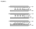
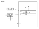
- Figure 1 illustrates schematically several embodiments (A,B,C) of methods for bonding discrete pads 30 of a bare die chip components (chips) 10 on a pad structure 40 of flexible substrate 20.
- the method has sufficient accuracy to correct for web deformations of the flexible substrate 20.
- the term "flexible substrate” used in this text refers in particular to a substrate that is bendable enough to be used in a reel to reel process.
- a flexible substrate as used in this text is a substrate that is flexible enough to allow bending over a certain curvature, e.g. with a radius of 1 - 100 centimeters (depending on the reel diameter), without the substrate losing essential functionality.
- Supply of chip bonding material matter 50 can be placed on the pad structure 40 ( Figure 1A ) or on chip pads 30 as for example illustrated in Figure 1B .
- the chips 10 may then be bonded on a pad structure 40 of the substrate 20 web directly.
- a composite pattern of conductive die bonding matter and structural adhesive 60 may be provided ( Figure 1C ).
- the method can be provided for interconnecting pad structures arranged on laminated flexible substrates.
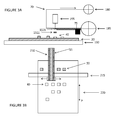
- Figure 2A and 2B show exemplary transfer setups for transferring die bonding matter 1511 to a pad structure 40 on a substrate 20 ( Figure A) or to pads 30 of bare die 10 ( Figure 2B ) for the method as presently claimed.
- a bonding method of a micro-electronic, in particular, a bare die component 10 is provided having one or more electrical connection pads, on a substrate 20 having on its substrate surface a connection pad structure 40 arranged for interconnecting the micro-electronic component via a respective one or more connection pads, the method comprising the steps of:
- a bonding method of a micro-electronic, in particular, a bare die component 10 is provided having one or more electrical connection pads, on a substrate 20 having on its substrate surface a connection pad structure 40 arranged for interconnecting the micro-electronic component via a respective one or more connection pads, the method comprising the steps of:
- the embodiments have as common concept that they provide for high speed high resolution bonding of micro-electronic components after placement thereof with their pads to respective pad structures of the substrate. Since the transferred adhesive or solder paste respectively remains intact, in particular, curable, or reflowable, during transfer, i.e. before placement, the bonding properties are optimal, so that after placement of the component 10 on the pad structure, the bonding matter, in particular, the adhesive or solder paste can be cured or reflowed respectively, to provide a robust bonding with electrical connectivity, that may have a bonding strength of more than 1 Mpa. This is a method that can be very efficient and cost effective for large scale industry purposes.
- a transparent carrier substrate 70 in the example, a quartz glass for a 248 nm KrF excimer and PET or Soda Lime Glass for a 355nm Nd:YAG laser.
- a conductive die attach die bonding material 15 is provided comprising a die bonding material layer 151 of a conductive thermosetting material or flux based solder paste and a dynamic release layer 152 adjacent to the conductive thermosetting or flux based solder material die bonding material layer 151.
- the dynamic release layer 152 is formed by a Triazene layer of about 100 nm thickness which functions as a sacrificial dynamic release layer (DRL), and comprises a polymer that, when photoactivated decomposes into nitrogen and other organic volatile gases 1521.
- DRL sacrificial dynamic release layer
- a typical peak absorption is found at 290-330 nm and the ablation threshold: 22-32 mJ/cm 2 at 308 -248 nm is quite low so that the donor die attach film layer or solder paste is not thermally loaded and remains intact after transfer, in such a way that the die bonding matter 1511 remains thermosettable.
- the laser beam may be restricted in timing and energy, in such a way that transferred bonding matter remains curable or consists of more than 10 % volume percent of solder flux. Accordingly a desired material property can be retained during transfer by impinging the laser beam on the dynamic release layer 151 adjacent to the conductive thermosettable material of die bonding material layer 15; in such a way that the dynamic release layer 152 is activated to direct the conductive die attach die bonding matter 1511 to cover a selected part of the substrate 20 with transferred conductive die bonding material.
- thermosettable isotropic conductive adhesive material 151 is transferred having electrical conductivity on for instance coated Cu substrates or silver tracks with a volume resistivity of typically 4-10 E-4 Ohm.cm and a typical curing temperature of 10 to 3 min @ 120-150 °C, commercially available as CE 3103 WLV from Henkel, with a viscosity of 15-25 Pa.s.
- another experimental conductive adhesive from Henkel is transferred consisting of a highly viscous conductive adhesive with a viscosity of 160 - 180 Pa.s that is cured in around 10 min at 150 °C.
- the conductive adhesive 151 is provided as homogenous layer of 20-30 micron, in particular, 25 micron thick provided on the dynamic release layer 152.
- the thickness is controlled to be around 25 um or 50 um but could be theoretically be of any thickness.
- the donor bonding materials are held at a distance of about 13-150 micron away from the substrate by shims 80.
- the conductive adhesive may also be replaced by a flux based Sn96.5Ag3Cu0.5 type 5 solder paste. Proper transfer of the solder with the flux can be achieved and functionality may be confirmed by reflow. Also nonconductive structural adhesives or pressure sensitive adhesives may be transferred successfully.
- the adhesive may have a viscosity of 1.2 Pa.s.
- a die bonding material layer may be a 15 -30 micron thick solid thermoplastic layer with a high conductivity of about 7 E-4 Ohm.cm and a curing schedule of about 1.5 h @ 175-200 °C.
- FIG 3A and 3B transfer systems are illustrated for transferring conductive thermosettable adhesives or solder paste from a tape 70 on a reel 185 and wound back to a reel 180.
- the bonding method as disclosed herein is adaptive and enables in combination with an alignment detection system accurate and adaptable corrections that renders it suitable for placement on a flexible foil wherein web integrity typically cannot be guaranteed.
- tape 70 can be made from PET foil and is passed through a donor feed system 75 where it is aligned under the beam of a laser 195 and transferred to pad structures 40 of an acceptor substrate 20.
- the substrate can be moved by a motorized stage 190 that can be moved in accordance with alignment control means that align the substrate 20 relative to the laser 195.
- Figure 3B show another example wherein a donor film 15 is moved by a motorized stage 220 having respective guides 210 and 215 for guiding the film in an X-Y fashion over a substrate 20.
- the substrate may be moving in a transport direction P by stage 220.
- the laser 195 may be moved mechanically or optically, so that the transfer of bonding matter 1511 can be aligned relative to the substrate 20.
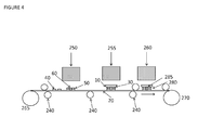
- FIG. 4 shows a schematic assembly process for a micro-electronic component 10 that includes transferring chip bonding and interconnect matter by the LIFT method in transfer section 250 as illustrated in the preceding.
- a bare chip component interconnection method is disclosed for the interconnecting and bonding a bare chip component 10 on a flexible substrate or foil 20 with conductive die attach matter 50 and nonconductive die attach matter 60.
- the method involves providing a flexible substrate 20 with contacts 40 and providing a bare chip component 10 with contacts 30 to be placed on a predefined placement by positioning means 255.
- the method involves a thermal exposure step 260 where the chip is permanently fixed by curing the conductive thermoset or reflowing solder melt 280 and optionally the thermoset nonconductive adhesive 285 before the flexible substrate said foil is wound back onto the reel 270.
- a substrate 20 or carrier web is unwound from a first reel 265 and guided via a set of guide rollers 240 to a second reel 270 to be wound up.
- various sub processes can be carried out, in particular, as one of the sub processes, bare chip component bonding as currently disclosed in the previous Figure 1 and 2 .
- these sub processes may involve:
- the chips 10 may be secured permanently to the substrate at the placement position e.g. by a bonding tool 260 such as a heater that activates the thermosetting material in the electrically conductive die bonding donor material that is thermosetting in a curing temperature region with a temperature elevated from the LIFT operating temperature in 260 so that the component is fixed by thermal curing, or any other known method for attaching chips to a (flexible) substrate.
- a bonding tool 260 such as a heater that activates the thermosetting material in the electrically conductive die bonding donor material that is thermosetting in a curing temperature region with a temperature elevated from the LIFT operating temperature in 260 so that the component is fixed by thermal curing, or any other known method for attaching chips to a (flexible) substrate.
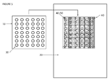
- the bump array consists of bumps 40 on a substrate 20 with diameters typically in the range of 10 to 500 micron.
- the density is preferably such that a sufficient number of bumps 30 are under a chip 10 to be placed. e.g. if the chip is of 1 mm edge length for instance a distance of 200 microns may be still sufficient (5 bumps x 5 bumps under the chip).
- Solder paste or thermosettable adhesive 50 bumps may be placed onto the bond pads or onto the substrate pads and subsequently the bump array 30 of the chip 10 may be placed and bonded onto the substrate by e.g. a flip chip method.
- structural adhesive 60 may be transferred for further structural bonding.
- microelectronic components such as passive components e.g. resistors, capacitors or inductors 310 or bare die LED's 410 may be placed on a prepatterned foil 20, wherein conductive adhesive or solder paste 50 and nonconductive adhesive 60 is applied by means of the above illustrated technique.
- Both the resistor 310 or bare die LED 410 are to be connected in the current example with the substrate foil 20 through conductive bumps to conductive tracks 40.
- circuits are advantageously applied on a flexible substrate to be applied e.g. on silver or copper tracks on PEN or PET foils.
- a typical chip height may vary e.g. between 0 - 250 micrometers.
- the bare die LED 410 has an anode bump 425 and cathode bump 426 of about 80x80 micron or even smaller to about 50x 50 micron, and a junction area 415 (LED part) of about 230 x 190 micron.
- the deposition step can be carried out as one embodiment of a method of treatment of bumps for chip dies in a chip manufacturing process.
- the method comprises clamping a wafer having identified bumps to be provided with a conductive adhesive; providing a conductive die attach donor film distanced from the wafer top surface; aligning the laser beam of the laser system and guiding the conductive die attach donor film relative to an identified bump on the wafer; and impinging a laser beam on a side of the conductive die attach donor film opposite a side facing the wafer; the laser beam tuned in timing, energy and direction to generate conductive die attach donor film matter directed towards a bump to be treated.
- a further embodiment involves a multishot process repeated steps are provided of guiding fresh conductive die attach donor film relative to the bump and impinging the laser beam on the conductive die attach donor film so as to direct a particle of conductive die bonding matter onto the bump.
- a laser repetition rate is preferably at least 60-600kHz .
- a conductive die attach donor film refreshment module with high refresh rate capabilities is very advantageous, for example having a conductive die attach donor film refreshment velocity relative to the bump of more than 0.1 m/s.
- the high laser repetition rate combined with a relative high number of about 60-200 of bumps provides an effective operation range for this chip bonding application competitive with stencil or screen printing and far superior to the deposition rate to that of jet printing with approx. 10 bumps per second .
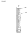
- Figure 7 shows an example of a structured donor film 70.
- the donor film may be provided in a premachined form, for example, comprising a sacrificial layer, a prepatterned conductive die bonding material layer provided in a matrix 15 of sacrificial material.
- a suitable thickness of the homogenous layer may range between 50 and 2000 nm, preferably in a range of 50-500 nm or even more preferably in a range of 50-250 nm.
- an embodiment for treatment of a bump can be carried out by stepping i.e. a non-roll to roll process.
- a fast beam modulator galvano mirror, polygon mirror, acousto-optic or electro-optic modulator etc.
- the modulator may be controlled in a feed forward process wherein bump coordinates are provided from an external source that provides the layout data of a chip die.
- the modulator can be used as a scanning unit that maps the bump coordinates in a prescan stage.
- an additional optical feedback system may provide laser alignment relative to the bump.
- a main beam is split into about 2-20 sub beams.
- each single bump may be treated by a multishot process where repeated steps are provided of guiding fresh conductive die attach die bonding material relative to the bump and generating a donor matter.
- the advantage of the disclosed laser transfer process over conventional printing is the range of use: for the intended features with a resolution ⁇ 50 ⁇ m stencil printing techniques generally fail (resolution spot size typically 75 ⁇ m) and jet printing even more (typical resolution spot size: 200 ⁇ m).
- the donor matter may have a wide-range of viscosity, possible to transfer (from 1 Pa.s to 160 Pa.s (non-exhaustive)).
- For stencil printing typical viscosities are >50 Pa.s and for Inkjet printing typical viscosities are ⁇ 0.1 Pa.s.
- Contrary to stencil printing and screen printing it is a non-contact direct write method with the possibility of on the fly correction for web deformations using a vision system.
Landscapes
- Engineering & Computer Science (AREA)
- Mechanical Engineering (AREA)
- Chemical & Material Sciences (AREA)
- Organic Chemistry (AREA)
- Electric Connection Of Electric Components To Printed Circuits (AREA)
- Wire Bonding (AREA)
- Manufacturing & Machinery (AREA)
Priority Applications (8)
| Application Number | Priority Date | Filing Date | Title |
|---|---|---|---|
| EP12192091.2A EP2731126A1 (en) | 2012-11-09 | 2012-11-09 | Method for bonding bare chip dies |
| CN201380065264.9A CN104854686B (zh) | 2012-11-09 | 2013-11-08 | 用于接合裸芯片模片的方法 |
| US14/441,714 US9859247B2 (en) | 2012-11-09 | 2013-11-08 | Method for bonding bare chip dies |
| PCT/NL2013/050800 WO2014073963A1 (en) | 2012-11-09 | 2013-11-08 | Method for bonding bare chip dies |
| KR1020157015349A KR102160321B1 (ko) | 2012-11-09 | 2013-11-08 | 베어 칩 다이 본딩 방법 |
| TW102140687A TWI674654B (zh) | 2012-11-09 | 2013-11-08 | 用以接合裸晶片晶粒之方法 |
| JP2015541717A JP6283679B2 (ja) | 2012-11-09 | 2013-11-08 | ベア・チップ・ダイをボンディングする方法 |
| EP13801876.7A EP2917931B1 (en) | 2012-11-09 | 2013-11-08 | Method for bonding bare chip dies |
Applications Claiming Priority (1)
| Application Number | Priority Date | Filing Date | Title |
|---|---|---|---|
| EP12192091.2A EP2731126A1 (en) | 2012-11-09 | 2012-11-09 | Method for bonding bare chip dies |
Publications (1)
| Publication Number | Publication Date |
|---|---|
| EP2731126A1 true EP2731126A1 (en) | 2014-05-14 |
Family
ID=47216108
Family Applications (2)
| Application Number | Title | Priority Date | Filing Date |
|---|---|---|---|
| EP12192091.2A Withdrawn EP2731126A1 (en) | 2012-11-09 | 2012-11-09 | Method for bonding bare chip dies |
| EP13801876.7A Active EP2917931B1 (en) | 2012-11-09 | 2013-11-08 | Method for bonding bare chip dies |
Family Applications After (1)
| Application Number | Title | Priority Date | Filing Date |
|---|---|---|---|
| EP13801876.7A Active EP2917931B1 (en) | 2012-11-09 | 2013-11-08 | Method for bonding bare chip dies |
Country Status (7)
| Country | Link |
|---|---|
| US (1) | US9859247B2 (https=) |
| EP (2) | EP2731126A1 (https=) |
| JP (1) | JP6283679B2 (https=) |
| KR (1) | KR102160321B1 (https=) |
| CN (1) | CN104854686B (https=) |
| TW (1) | TWI674654B (https=) |
| WO (1) | WO2014073963A1 (https=) |
Cited By (2)
| Publication number | Priority date | Publication date | Assignee | Title |
|---|---|---|---|---|
| US20220399298A1 (en) * | 2021-06-15 | 2022-12-15 | International Business Machines Corporation | Solder transfer integrated circuit packaging |
| WO2023001927A1 (de) * | 2021-07-23 | 2023-01-26 | Osram Opto Semiconductors Gmbh | Verfahren zum aufbringen eines elektrischen verbindungsmaterials oder flussmittels auf ein bauelement |
Families Citing this family (29)
| Publication number | Priority date | Publication date | Assignee | Title |
|---|---|---|---|---|
| ES2471568B1 (es) * | 2012-11-22 | 2015-08-21 | Abengoa Solar New Technologies S.A. | Procedimiento para la creación de contactos eléctricos y contactos así creados |
| TWI561325B (en) * | 2014-08-01 | 2016-12-11 | Au Optronics Corp | Display module manufacturing method and display module |
| CN106716611B (zh) | 2014-10-17 | 2019-08-20 | 英特尔公司 | 微拾取和键合组装 |
| US10471538B2 (en) * | 2015-07-09 | 2019-11-12 | Orbotech Ltd. | Control of lift ejection angle |
| DE102016103324A1 (de) * | 2016-02-25 | 2017-08-31 | Osram Opto Semiconductors Gmbh | Videowand-Modul und Verfahren zum Herstellen eines Videowand-Moduls |
| US9916989B2 (en) | 2016-04-15 | 2018-03-13 | Amkor Technology, Inc. | System and method for laser assisted bonding of semiconductor die |
| WO2017188125A1 (ja) * | 2016-04-27 | 2017-11-02 | セイコーエプソン株式会社 | 実装構造体、超音波デバイス、超音波探触子、超音波装置、及び電子機器 |
| US10032827B2 (en) * | 2016-06-29 | 2018-07-24 | Applied Materials, Inc. | Systems and methods for transfer of micro-devices |
| WO2018094504A1 (en) * | 2016-11-23 | 2018-05-31 | Institut National De La Recherche Scientifique | Method and system of laser-driven impact acceleration |
| CN108346640B (zh) * | 2017-01-25 | 2020-02-07 | 华邦电子股份有限公司 | 半导体结构及其制作方法 |
| KR20240130146A (ko) | 2017-06-12 | 2024-08-28 | 쿨리케 & 소파 네덜란드 비.브이. | 개별 부품들의 기판 상으로의 병렬적 조립 |
| US11201077B2 (en) | 2017-06-12 | 2021-12-14 | Kulicke & Soffa Netherlands B.V. | Parallel assembly of discrete components onto a substrate |
| WO2018227453A1 (en) * | 2017-06-15 | 2018-12-20 | Goertek Inc. | Method for transferring micro-light emitting diodes, micro-light emitting diode device and electronic device |
| US10163773B1 (en) | 2017-08-11 | 2018-12-25 | General Electric Company | Electronics package having a self-aligning interconnect assembly and method of making same |
| CN109994413A (zh) * | 2017-12-29 | 2019-07-09 | 南昌欧菲显示科技有限公司 | 微型元件巨量转移方法 |
| TWI688317B (zh) * | 2018-10-31 | 2020-03-11 | 台灣愛司帝科技股份有限公司 | 發光二極體晶片的固接方法及固接裝置 |
| CN113690149A (zh) * | 2020-05-16 | 2021-11-23 | 佛山市国星光电股份有限公司 | 一种芯片键合结构、方法及设备 |
| CN115702488A (zh) * | 2020-06-04 | 2023-02-14 | 奥宝科技有限公司 | 高分辨率焊接 |
| US11627667B2 (en) * | 2021-01-29 | 2023-04-11 | Orbotech Ltd. | High-resolution soldering |
| US20220347778A1 (en) * | 2020-06-28 | 2022-11-03 | Orbotech Ltd. | Laser Printing of Solder Pastes |
| WO2022063431A1 (en) | 2020-09-22 | 2022-03-31 | Kulicke & Soffa Netherlands B.V. | Reusable die catch materials, reusable die release materials, related die transfer systems, and methods of using the same |
| CN113451274B (zh) * | 2020-10-28 | 2022-08-05 | 重庆康佳光电技术研究院有限公司 | Led芯片组件、显示面板及制备方法 |
| CN116072794A (zh) * | 2021-11-02 | 2023-05-05 | 重庆康佳光电技术研究院有限公司 | 显示面板修补方法及系统 |
| TW202343603A (zh) * | 2022-02-18 | 2023-11-01 | 日商迪睿合股份有限公司 | 連接結構體之製造方法及單片化接著膜之轉印方法 |
| IT202200009839A1 (it) * | 2022-05-12 | 2023-11-12 | St Microelectronics Srl | Procedimento per fabbricare dispositivi a semiconduttore e dispositivo a semiconduttore corrispondente |
| CN117059497B (zh) * | 2022-05-12 | 2026-02-27 | 意法半导体股份有限公司 | 制造半导体设备的方法和对应的半导体设备 |
| CN115579440B (zh) * | 2022-12-09 | 2023-07-18 | 惠科股份有限公司 | Led芯片、刷料装置及led芯片的刷料固晶方法 |
| CN116364561B (zh) * | 2023-06-01 | 2023-09-08 | 湖北三维半导体集成创新中心有限责任公司 | 键合方法及键合结构 |
| US20250011166A1 (en) * | 2023-07-03 | 2025-01-09 | Massachusetts Institute Of Technology | Additive manufacturing using bonding of voxels and related systems, devices, and articles |
Citations (7)
| Publication number | Priority date | Publication date | Assignee | Title |
|---|---|---|---|---|
| JPH0837206A (ja) * | 1994-07-22 | 1996-02-06 | Nec Corp | 半導体装置の製造方法 |
| WO1998005068A1 (en) * | 1996-07-26 | 1998-02-05 | Philips Electronics N.V. | Method of manufacturing and transferring metallic droplets |
| JPH1070151A (ja) * | 1996-08-26 | 1998-03-10 | Ricoh Co Ltd | 導電粒子の配列方法及びその装置 |
| US5873511A (en) * | 1997-05-08 | 1999-02-23 | Shapiro; Herbert M. | Apparatus and method for forming solder bonding pads |
| US20060035454A1 (en) * | 2004-08-16 | 2006-02-16 | Ibm Corporation | Fluxless solder transfer and reflow process |
| US7348270B1 (en) * | 2007-01-22 | 2008-03-25 | International Business Machines Corporation | Techniques for forming interconnects |
| EP2487215A1 (en) * | 2011-02-11 | 2012-08-15 | Henkel AG & Co. KGaA | Electrically conductive adhesives comprising at least one metal precursor |
Family Cites Families (62)
| Publication number | Priority date | Publication date | Assignee | Title |
|---|---|---|---|---|
| GB1138084A (en) | 1966-07-22 | 1968-12-27 | Standard Telephones Cables Ltd | Method of vapour depositing a material in the form of a pattern |
| US4752455A (en) | 1986-05-27 | 1988-06-21 | Kms Fusion, Inc. | Pulsed laser microfabrication |
| US6537720B1 (en) | 1989-03-30 | 2003-03-25 | Polaroid Graphics Imaging Llc | Ablation-transfer imaging/recording |
| US4987006A (en) | 1990-03-26 | 1991-01-22 | Amp Incorporated | Laser transfer deposition |
| DK0713586T3 (da) | 1993-08-13 | 2001-09-24 | Pgi Graphics Imaging Llc | Ablationsoverføring til mellemreceptorer |
| DE4330961C1 (de) | 1993-09-09 | 1994-07-28 | Krone Ag | Verfahren zur Herstellung von strukturierten Metallisierungen auf Oberflächen |
| US5685939A (en) * | 1995-03-10 | 1997-11-11 | Minnesota Mining And Manufacturing Company | Process for making a Z-axis adhesive and establishing electrical interconnection therewith |
| JPH09129649A (ja) * | 1995-11-06 | 1997-05-16 | Matsushita Electric Ind Co Ltd | 接合材料供給方法及び実装方法 |
| US6159832A (en) | 1998-03-18 | 2000-12-12 | Mayer; Frederick J. | Precision laser metallization |
| US6060127A (en) | 1998-03-31 | 2000-05-09 | Matsushita Electric Industrial Co., Ltd. | Mechanically restricted laser deposition |
| AU2514900A (en) | 1999-01-27 | 2000-08-18 | United States Of America As Represented By The Secretary Of The Navy, The | Fabrication of conductive/non-conductive nanocomposites by laser evaporation |
| US6936311B2 (en) | 1999-01-27 | 2005-08-30 | The United States Of America As Represented By The Secretary Of The Navy | Generation of biomaterial microarrays by laser transfer |
| US6792326B1 (en) * | 1999-05-24 | 2004-09-14 | Potomac Photonics, Inc. | Material delivery system for miniature structure fabrication |
| US7014885B1 (en) | 1999-07-19 | 2006-03-21 | The United States Of America As Represented By The Secretary Of The Navy | Direct-write laser transfer and processing |
| DE19946182C2 (de) | 1999-09-21 | 2003-07-03 | Forschungsverbund Berlin Ev | Verfahren zur Herstellung von Kohlenstoff Nanoröhren |
| JP2001237279A (ja) | 2000-02-23 | 2001-08-31 | Hitachi Ltd | 半導体装置及びそれを用いた電子装置 |
| US6649861B2 (en) | 2000-05-24 | 2003-11-18 | Potomac Photonics, Inc. | Method and apparatus for fabrication of miniature structures |
| AU2000261986A1 (en) | 2000-07-20 | 2003-12-12 | The United States Of America As Represented By The Secretary Of The Navy | Direct-write laser transfer and processing |
| JP2003077940A (ja) | 2001-09-06 | 2003-03-14 | Sony Corp | 素子の転写方法及びこれを用いた素子の配列方法、画像表示装置の製造方法 |
| AT411755B (de) | 2001-12-21 | 2004-05-25 | Baeuerle Dieter Dr | Vorrichtung und verfahren zum modifizieren einer werkstück-oberfläche mit hilfe von photonen-strahlung |
| GR1004059B (el) | 2001-12-31 | 2002-11-15 | Ιωαννα Ζεργιωτη | Κατασκευη βιοπολυμερικων σχηματων μεσω εναποθεσης με λειζερ. |
| US6703179B2 (en) | 2002-03-13 | 2004-03-09 | Eastman Kodak Company | Transfer of organic material from a donor to form a layer in an OLED device |
| US20040022947A1 (en) | 2002-08-01 | 2004-02-05 | Duignan Michael T. | Method for creating microstructure patterns by contact transfer technique |
| US6939660B2 (en) | 2002-08-02 | 2005-09-06 | Eastman Kodak Company | Laser thermal transfer donor including a separate dopant layer |
| DE10237732B4 (de) | 2002-08-17 | 2004-08-26 | BLZ Bayerisches Laserzentrum Gemeinnützige Forschungsgesellschaft mbH | Laserstrahlmarkierungsverfahren sowie Markierungsvorrichtung zur Laserstrahlmarkierung eines Zielsubstrats |
| US20040250769A1 (en) | 2002-10-28 | 2004-12-16 | Finisar Corporation | Pulsed laser deposition for mass production |
| WO2004080725A1 (en) | 2003-03-13 | 2004-09-23 | Koninklijke Philips Electronics N.V. | Marking method and market object |
| US7381440B2 (en) | 2003-06-06 | 2008-06-03 | The United States Of America As Represented By The Secretary Of The Navy | Biological laser printing for tissue microdissection via indirect photon-biomaterial interactions |
| US8075958B2 (en) | 2003-07-29 | 2011-12-13 | Intelligent Energy, Inc. | Methods for providing thin hydrogen separation membranes and associated uses |
| WO2005024908A2 (en) | 2003-09-05 | 2005-03-17 | Si2 Technologies, Inc. | Laser transfer articles and method of making |
| US6962765B2 (en) | 2003-10-20 | 2005-11-08 | Kodak Polychrome Graphics Llc | Laser-generated ultraviolet radiation mask |
| US7485337B2 (en) | 2004-05-27 | 2009-02-03 | Eastman Kodak Company | Depositing an organic layer for use in OLEDs |
| US7461938B2 (en) | 2004-06-30 | 2008-12-09 | Ophthonix, Inc. | Apparatus and method for determining sphere and cylinder components of subjective refraction using objective wavefront measurement |
| US7358169B2 (en) | 2005-04-13 | 2008-04-15 | Hewlett-Packard Development Company, L.P. | Laser-assisted deposition |
| GB0525847D0 (en) | 2005-12-20 | 2006-02-01 | Univ Bristol | Parallel Laser Direct Write |
| TWI431380B (zh) | 2006-05-12 | 2014-03-21 | 光子動力公司 | 沉積修復設備及方法 |
| CN101517700B (zh) | 2006-09-20 | 2014-04-16 | 伊利诺伊大学评议会 | 用于制造可转移半导体结构、器件和器件构件的松脱策略 |
| KR101563237B1 (ko) | 2007-06-01 | 2015-10-26 | 가부시키가이샤 한도오따이 에네루기 켄큐쇼 | 제조장치 및 발광장치 제작방법 |
| WO2008157666A1 (en) | 2007-06-19 | 2008-12-24 | The Government Of The United States Of America, As Represented By The Secretary Of The Navy | Sub-micron laser direct write |
| US8728589B2 (en) | 2007-09-14 | 2014-05-20 | Photon Dynamics, Inc. | Laser decal transfer of electronic materials |
| US20090130427A1 (en) | 2007-10-22 | 2009-05-21 | The Regents Of The University Of California | Nanomaterial facilitated laser transfer |
| KR20090041314A (ko) | 2007-10-23 | 2009-04-28 | 가부시키가이샤 한도오따이 에네루기 켄큐쇼 | 증착용 기판 및 발광장치의 제조방법 |
| TWI375498B (en) | 2007-11-21 | 2012-10-21 | Ind Tech Res Inst | High perfromance laser-assisted transferring system and transfer component |
| TW200945339A (en) | 2007-12-19 | 2009-11-01 | Koninkl Philips Electronics Nv | Optical disk format for direct writing materials on a substrate |
| KR101689519B1 (ko) | 2007-12-26 | 2016-12-26 | 가부시키가이샤 한도오따이 에네루기 켄큐쇼 | 증착용 기판, 증착용 기판의 제조방법, 및 발광장치의 제조방법 |
| DE102008057228A1 (de) | 2008-01-17 | 2009-07-23 | Schmid Technology Gmbh | Verfahren und Vorrichtung zur Herstellung einer Solarzelle |
| US8056222B2 (en) | 2008-02-20 | 2011-11-15 | The United States Of America, As Represented By The Secretary Of The Navy | Laser-based technique for the transfer and embedding of electronic components and devices |
| JP5238544B2 (ja) | 2008-03-07 | 2013-07-17 | 株式会社半導体エネルギー研究所 | 成膜方法及び発光装置の作製方法 |
| US7919340B2 (en) | 2008-06-04 | 2011-04-05 | Semiconductor Energy Laboratory Co., Ltd. | Method for manufacturing light-emitting device |
| DE102008026727B3 (de) | 2008-06-04 | 2009-07-30 | Technische Universität Carolo-Wilhelmina Zu Braunschweig | Trägersystem für die Lasermikrodissektion und den laserinduzierten Transport von biologischem Material und lebenden Zellen |
| US20110089412A1 (en) | 2008-06-16 | 2011-04-21 | Shigeo Fujimori | Patterning method, production method of device using the patterning method, and device |
| WO2009153792A2 (en) | 2008-06-19 | 2009-12-23 | Utilight Ltd. | Light induced patterning |
| US20100123258A1 (en) * | 2008-11-14 | 2010-05-20 | Myung Jin Yim | Low Temperature Board Level Assembly Using Anisotropically Conductive Materials |
| US8663754B2 (en) | 2009-03-09 | 2014-03-04 | Imra America, Inc. | Pulsed laser micro-deposition pattern formation |
| US8021919B2 (en) | 2009-03-31 | 2011-09-20 | Infineon Technologies Ag | Method of manufacturing a semiconductor device |
| ES2360778B1 (es) | 2009-07-22 | 2012-05-03 | Universidad De Barcelona | Aparato y método para la impresión directa con l�?ser. |
| JP5323784B2 (ja) | 2009-09-15 | 2013-10-23 | フオン・アルデンネ・アンラーゲンテヒニク・ゲゼルシヤフト・ミト・ベシユレンクテル・ハフツング | 微細構造を製造するための方法及び装置 |
| US9039998B2 (en) | 2010-03-04 | 2015-05-26 | Institut National De La Sante Et De La Recherche Medical (Inserm) | Bioprinting station, assembly comprising such bioprinting station and bioprinting method |
| US9496155B2 (en) | 2010-03-29 | 2016-11-15 | Semprius, Inc. | Methods of selectively transferring active components |
| US20110278566A1 (en) | 2010-05-17 | 2011-11-17 | Industry-Academic Cooperation Foundation, Yonsei University | Method of patterning thin film solution-deposited |
| GB201009847D0 (en) | 2010-06-11 | 2010-07-21 | Dzp Technologies Ltd | Deposition method, apparatus, printed object and uses |
| DE102010043204A1 (de) | 2010-08-10 | 2012-02-16 | Von Ardenne Anlagentechnik Gmbh | Verfahren und Verwendung einer Vorrichtung zur Erzeugung einer Schicht eines organischen Materials auf einem Substrat |
-
2012
- 2012-11-09 EP EP12192091.2A patent/EP2731126A1/en not_active Withdrawn
-
2013
- 2013-11-08 EP EP13801876.7A patent/EP2917931B1/en active Active
- 2013-11-08 US US14/441,714 patent/US9859247B2/en active Active
- 2013-11-08 KR KR1020157015349A patent/KR102160321B1/ko active Active
- 2013-11-08 TW TW102140687A patent/TWI674654B/zh active
- 2013-11-08 CN CN201380065264.9A patent/CN104854686B/zh active Active
- 2013-11-08 WO PCT/NL2013/050800 patent/WO2014073963A1/en not_active Ceased
- 2013-11-08 JP JP2015541717A patent/JP6283679B2/ja active Active
Patent Citations (7)
| Publication number | Priority date | Publication date | Assignee | Title |
|---|---|---|---|---|
| JPH0837206A (ja) * | 1994-07-22 | 1996-02-06 | Nec Corp | 半導体装置の製造方法 |
| WO1998005068A1 (en) * | 1996-07-26 | 1998-02-05 | Philips Electronics N.V. | Method of manufacturing and transferring metallic droplets |
| JPH1070151A (ja) * | 1996-08-26 | 1998-03-10 | Ricoh Co Ltd | 導電粒子の配列方法及びその装置 |
| US5873511A (en) * | 1997-05-08 | 1999-02-23 | Shapiro; Herbert M. | Apparatus and method for forming solder bonding pads |
| US20060035454A1 (en) * | 2004-08-16 | 2006-02-16 | Ibm Corporation | Fluxless solder transfer and reflow process |
| US7348270B1 (en) * | 2007-01-22 | 2008-03-25 | International Business Machines Corporation | Techniques for forming interconnects |
| EP2487215A1 (en) * | 2011-02-11 | 2012-08-15 | Henkel AG & Co. KGaA | Electrically conductive adhesives comprising at least one metal precursor |
Non-Patent Citations (1)
| Title |
|---|
| PIQUE ET AL.: "Three- Dimensional Printing of Interconnects by Laser Direct- Write of Silver Nanopastes", ADVANCED MATERIALS, vol. 22, no. 40, 25 October 2010 (2010-10-25), pages 4462 - 4466 |
Cited By (3)
| Publication number | Priority date | Publication date | Assignee | Title |
|---|---|---|---|---|
| US20220399298A1 (en) * | 2021-06-15 | 2022-12-15 | International Business Machines Corporation | Solder transfer integrated circuit packaging |
| US11631650B2 (en) * | 2021-06-15 | 2023-04-18 | International Business Machines Corporation | Solder transfer integrated circuit packaging |
| WO2023001927A1 (de) * | 2021-07-23 | 2023-01-26 | Osram Opto Semiconductors Gmbh | Verfahren zum aufbringen eines elektrischen verbindungsmaterials oder flussmittels auf ein bauelement |
Also Published As
| Publication number | Publication date |
|---|---|
| EP2917931B1 (en) | 2023-08-02 |
| US9859247B2 (en) | 2018-01-02 |
| JP6283679B2 (ja) | 2018-02-21 |
| CN104854686A (zh) | 2015-08-19 |
| CN104854686B (zh) | 2018-11-27 |
| EP2917931A1 (en) | 2015-09-16 |
| WO2014073963A1 (en) | 2014-05-15 |
| US20150294951A1 (en) | 2015-10-15 |
| TWI674654B (zh) | 2019-10-11 |
| TW201426920A (zh) | 2014-07-01 |
| KR20150106875A (ko) | 2015-09-22 |
| JP2015534285A (ja) | 2015-11-26 |
| KR102160321B1 (ko) | 2020-09-28 |
Similar Documents
| Publication | Publication Date | Title |
|---|---|---|
| US9859247B2 (en) | Method for bonding bare chip dies | |
| CN110637354B (zh) | 于未事先图样化的基板上电器互连的电路元件 | |
| US8735218B2 (en) | Method and apparatus for manufacturing an electronic assembly, electronic assembly manufactured with the method or in the apparatus | |
| KR20210027848A (ko) | 마이크로 엘이디 디스플레이 및 이의 제작 방법 | |
| EP1720389B1 (en) | Method for forming pattern and a wired board | |
| KR102858957B1 (ko) | 광학 시스템 특성의 조정에 의해 개별 콤포넌트의 어셈블레에서의 위치 오차 보상 | |
| KR20170057909A (ko) | 반도체 패키지의 제조 방법 | |
| KR102403569B1 (ko) | 열압착 본더, 열압착 본더 작동 방법, 및 미세 피치의 플립 칩 조립체 상호 접속 방법 | |
| US11877398B2 (en) | PCB production by laser systems | |
| Zacharatos et al. | Laser-induced forward transfer (LIFT) technique as an alternative for assembly and packaging of electronic components | |
| US20240324101A1 (en) | Pcb production by laser systems | |
| CN104349602A (zh) | 薄膜形成方法及薄膜形成装置 | |
| US20240332233A1 (en) | Method of bonding column type deposits | |
| CN116830812A (zh) | 利用激光系统进行pcb生产 | |
| JP2013225656A (ja) | 半導体回路構造体及びその製造方法 | |
| US20230240022A1 (en) | Hybrid process for pcb production by lad system | |
| WO2021075051A1 (ja) | 部品装着方法、および部品装着装置 | |
| Arutinov et al. | Integration with Light | |
| JP2015012056A (ja) | 半田ボール搭載方法 | |
| JPH11354914A (ja) | 電子部品実装方法 |
Legal Events
| Date | Code | Title | Description |
|---|---|---|---|
| PUAI | Public reference made under article 153(3) epc to a published international application that has entered the european phase |
Free format text: ORIGINAL CODE: 0009012 |
|
| 17P | Request for examination filed |
Effective date: 20121109 |
|
| AK | Designated contracting states |
Kind code of ref document: A1 Designated state(s): AL AT BE BG CH CY CZ DE DK EE ES FI FR GB GR HR HU IE IS IT LI LT LU LV MC MK MT NL NO PL PT RO RS SE SI SK SM TR |
|
| AX | Request for extension of the european patent |
Extension state: BA ME |
|
| STAA | Information on the status of an ep patent application or granted ep patent |
Free format text: STATUS: THE APPLICATION IS DEEMED TO BE WITHDRAWN |
|
| 18D | Application deemed to be withdrawn |
Effective date: 20141115 |