US9859247B2 - Method for bonding bare chip dies - Google Patents
Method for bonding bare chip dies Download PDFInfo
- Publication number
- US9859247B2 US9859247B2 US14/441,714 US201314441714A US9859247B2 US 9859247 B2 US9859247 B2 US 9859247B2 US 201314441714 A US201314441714 A US 201314441714A US 9859247 B2 US9859247 B2 US 9859247B2
- Authority
- US
- United States
- Prior art keywords
- pad structure
- micro
- bonding
- bonding material
- electronic component
- Prior art date
- Legal status (The legal status is an assumption and is not a legal conclusion. Google has not performed a legal analysis and makes no representation as to the accuracy of the status listed.)
- Active, expires
Links
Images


Classifications
-
- H—ELECTRICITY
- H01—ELECTRIC ELEMENTS
- H01L—SEMICONDUCTOR DEVICES NOT COVERED BY CLASS H10
- H01L24/00—Arrangements for connecting or disconnecting semiconductor or solid-state bodies; Methods or apparatus related thereto
- H01L24/80—Methods for connecting semiconductor or other solid state bodies using means for bonding being attached to, or being formed on, the surface to be connected
- H01L24/83—Methods for connecting semiconductor or other solid state bodies using means for bonding being attached to, or being formed on, the surface to be connected using a layer connector
-
- B—PERFORMING OPERATIONS; TRANSPORTING
- B23—MACHINE TOOLS; METAL-WORKING NOT OTHERWISE PROVIDED FOR
- B23K—SOLDERING OR UNSOLDERING; WELDING; CLADDING OR PLATING BY SOLDERING OR WELDING; CUTTING BY APPLYING HEAT LOCALLY, e.g. FLAME CUTTING; WORKING BY LASER BEAM
- B23K35/00—Rods, electrodes, materials, or media, for use in soldering, welding, or cutting
- B23K35/02—Rods, electrodes, materials, or media, for use in soldering, welding, or cutting characterised by mechanical features, e.g. shape
-
- B—PERFORMING OPERATIONS; TRANSPORTING
- B23—MACHINE TOOLS; METAL-WORKING NOT OTHERWISE PROVIDED FOR
- B23K—SOLDERING OR UNSOLDERING; WELDING; CLADDING OR PLATING BY SOLDERING OR WELDING; CUTTING BY APPLYING HEAT LOCALLY, e.g. FLAME CUTTING; WORKING BY LASER BEAM
- B23K35/00—Rods, electrodes, materials, or media, for use in soldering, welding, or cutting
- B23K35/22—Rods, electrodes, materials, or media, for use in soldering, welding, or cutting characterised by the composition or nature of the material
- B23K35/24—Selection of soldering or welding materials proper
- B23K35/26—Selection of soldering or welding materials proper with the principal constituent melting at less than 400 degrees C
- B23K35/262—Sn as the principal constituent
-
- C—CHEMISTRY; METALLURGY
- C09—DYES; PAINTS; POLISHES; NATURAL RESINS; ADHESIVES; COMPOSITIONS NOT OTHERWISE PROVIDED FOR; APPLICATIONS OF MATERIALS NOT OTHERWISE PROVIDED FOR
- C09J—ADHESIVES; NON-MECHANICAL ASPECTS OF ADHESIVE PROCESSES IN GENERAL; ADHESIVE PROCESSES NOT PROVIDED FOR ELSEWHERE; USE OF MATERIALS AS ADHESIVES
- C09J5/00—Adhesive processes in general; Adhesive processes not provided for elsewhere, e.g. relating to primers
- C09J5/06—Adhesive processes in general; Adhesive processes not provided for elsewhere, e.g. relating to primers involving heating of the applied adhesive
-
- H—ELECTRICITY
- H01—ELECTRIC ELEMENTS
- H01L—SEMICONDUCTOR DEVICES NOT COVERED BY CLASS H10
- H01L21/00—Processes or apparatus adapted for the manufacture or treatment of semiconductor or solid state devices or of parts thereof
- H01L21/02—Manufacture or treatment of semiconductor devices or of parts thereof
- H01L21/04—Manufacture or treatment of semiconductor devices or of parts thereof the devices having at least one potential-jump barrier or surface barrier, e.g. PN junction, depletion layer or carrier concentration layer
- H01L21/48—Manufacture or treatment of parts, e.g. containers, prior to assembly of the devices, using processes not provided for in a single one of the subgroups H01L21/06 - H01L21/326
- H01L21/4814—Conductive parts
- H01L21/4846—Leads on or in insulating or insulated substrates, e.g. metallisation
- H01L21/4853—Connection or disconnection of other leads to or from a metallisation, e.g. pins, wires, bumps
-
- H—ELECTRICITY
- H01—ELECTRIC ELEMENTS
- H01L—SEMICONDUCTOR DEVICES NOT COVERED BY CLASS H10
- H01L21/00—Processes or apparatus adapted for the manufacture or treatment of semiconductor or solid state devices or of parts thereof
- H01L21/02—Manufacture or treatment of semiconductor devices or of parts thereof
- H01L21/04—Manufacture or treatment of semiconductor devices or of parts thereof the devices having at least one potential-jump barrier or surface barrier, e.g. PN junction, depletion layer or carrier concentration layer
- H01L21/50—Assembly of semiconductor devices using processes or apparatus not provided for in a single one of the subgroups H01L21/06 - H01L21/326, e.g. sealing of a cap to a base of a container
-
- H—ELECTRICITY
- H01—ELECTRIC ELEMENTS
- H01L—SEMICONDUCTOR DEVICES NOT COVERED BY CLASS H10
- H01L23/00—Details of semiconductor or other solid state devices
- H01L23/48—Arrangements for conducting electric current to or from the solid state body in operation, e.g. leads, terminal arrangements ; Selection of materials therefor
- H01L23/488—Arrangements for conducting electric current to or from the solid state body in operation, e.g. leads, terminal arrangements ; Selection of materials therefor consisting of soldered or bonded constructions
- H01L23/498—Leads, i.e. metallisations or lead-frames on insulating substrates, e.g. chip carriers
- H01L23/49811—Additional leads joined to the metallisation on the insulating substrate, e.g. pins, bumps, wires, flat leads
- H01L23/49816—Spherical bumps on the substrate for external connection, e.g. ball grid arrays [BGA]
-
- H—ELECTRICITY
- H01—ELECTRIC ELEMENTS
- H01L—SEMICONDUCTOR DEVICES NOT COVERED BY CLASS H10
- H01L24/00—Arrangements for connecting or disconnecting semiconductor or solid-state bodies; Methods or apparatus related thereto
- H01L24/01—Means for bonding being attached to, or being formed on, the surface to be connected, e.g. chip-to-package, die-attach, "first-level" interconnects; Manufacturing methods related thereto
- H01L24/10—Bump connectors ; Manufacturing methods related thereto
- H01L24/11—Manufacturing methods
-
- H—ELECTRICITY
- H01—ELECTRIC ELEMENTS
- H01L—SEMICONDUCTOR DEVICES NOT COVERED BY CLASS H10
- H01L24/00—Arrangements for connecting or disconnecting semiconductor or solid-state bodies; Methods or apparatus related thereto
- H01L24/01—Means for bonding being attached to, or being formed on, the surface to be connected, e.g. chip-to-package, die-attach, "first-level" interconnects; Manufacturing methods related thereto
- H01L24/26—Layer connectors, e.g. plate connectors, solder or adhesive layers; Manufacturing methods related thereto
- H01L24/27—Manufacturing methods
-
- C09J2201/61—
-
- C—CHEMISTRY; METALLURGY
- C09—DYES; PAINTS; POLISHES; NATURAL RESINS; ADHESIVES; COMPOSITIONS NOT OTHERWISE PROVIDED FOR; APPLICATIONS OF MATERIALS NOT OTHERWISE PROVIDED FOR
- C09J—ADHESIVES; NON-MECHANICAL ASPECTS OF ADHESIVE PROCESSES IN GENERAL; ADHESIVE PROCESSES NOT PROVIDED FOR ELSEWHERE; USE OF MATERIALS AS ADHESIVES
- C09J2203/00—Applications of adhesives in processes or use of adhesives in the form of films or foils
- C09J2203/326—Applications of adhesives in processes or use of adhesives in the form of films or foils for bonding electronic components such as wafers, chips or semiconductors
-
- C09J2205/31—
-
- C—CHEMISTRY; METALLURGY
- C09—DYES; PAINTS; POLISHES; NATURAL RESINS; ADHESIVES; COMPOSITIONS NOT OTHERWISE PROVIDED FOR; APPLICATIONS OF MATERIALS NOT OTHERWISE PROVIDED FOR
- C09J—ADHESIVES; NON-MECHANICAL ASPECTS OF ADHESIVE PROCESSES IN GENERAL; ADHESIVE PROCESSES NOT PROVIDED FOR ELSEWHERE; USE OF MATERIALS AS ADHESIVES
- C09J2301/00—Additional features of adhesives in the form of films or foils
- C09J2301/30—Additional features of adhesives in the form of films or foils characterized by the chemical, physicochemical or physical properties of the adhesive or the carrier
- C09J2301/304—Additional features of adhesives in the form of films or foils characterized by the chemical, physicochemical or physical properties of the adhesive or the carrier the adhesive being heat-activatable, i.e. not tacky at temperatures inferior to 30°C
-
- C—CHEMISTRY; METALLURGY
- C09—DYES; PAINTS; POLISHES; NATURAL RESINS; ADHESIVES; COMPOSITIONS NOT OTHERWISE PROVIDED FOR; APPLICATIONS OF MATERIALS NOT OTHERWISE PROVIDED FOR
- C09J—ADHESIVES; NON-MECHANICAL ASPECTS OF ADHESIVE PROCESSES IN GENERAL; ADHESIVE PROCESSES NOT PROVIDED FOR ELSEWHERE; USE OF MATERIALS AS ADHESIVES
- C09J2301/00—Additional features of adhesives in the form of films or foils
- C09J2301/40—Additional features of adhesives in the form of films or foils characterized by the presence of essential components
- C09J2301/416—Additional features of adhesives in the form of films or foils characterized by the presence of essential components use of irradiation
-
- H—ELECTRICITY
- H01—ELECTRIC ELEMENTS
- H01L—SEMICONDUCTOR DEVICES NOT COVERED BY CLASS H10
- H01L21/00—Processes or apparatus adapted for the manufacture or treatment of semiconductor or solid state devices or of parts thereof
- H01L21/02—Manufacture or treatment of semiconductor devices or of parts thereof
- H01L21/04—Manufacture or treatment of semiconductor devices or of parts thereof the devices having at least one potential-jump barrier or surface barrier, e.g. PN junction, depletion layer or carrier concentration layer
- H01L21/50—Assembly of semiconductor devices using processes or apparatus not provided for in a single one of the subgroups H01L21/06 - H01L21/326, e.g. sealing of a cap to a base of a container
- H01L21/60—Attaching or detaching leads or other conductive members, to be used for carrying current to or from the device in operation
- H01L2021/60277—Attaching or detaching leads or other conductive members, to be used for carrying current to or from the device in operation involving the use of conductive adhesives
-
- H—ELECTRICITY
- H01—ELECTRIC ELEMENTS
- H01L—SEMICONDUCTOR DEVICES NOT COVERED BY CLASS H10
- H01L21/00—Processes or apparatus adapted for the manufacture or treatment of semiconductor or solid state devices or of parts thereof
- H01L21/02—Manufacture or treatment of semiconductor devices or of parts thereof
- H01L21/04—Manufacture or treatment of semiconductor devices or of parts thereof the devices having at least one potential-jump barrier or surface barrier, e.g. PN junction, depletion layer or carrier concentration layer
- H01L21/50—Assembly of semiconductor devices using processes or apparatus not provided for in a single one of the subgroups H01L21/06 - H01L21/326, e.g. sealing of a cap to a base of a container
- H01L21/56—Encapsulations, e.g. encapsulation layers, coatings
- H01L21/563—Encapsulation of active face of flip-chip device, e.g. underfilling or underencapsulation of flip-chip, encapsulation preform on chip or mounting substrate
-
- H—ELECTRICITY
- H01—ELECTRIC ELEMENTS
- H01L—SEMICONDUCTOR DEVICES NOT COVERED BY CLASS H10
- H01L21/00—Processes or apparatus adapted for the manufacture or treatment of semiconductor or solid state devices or of parts thereof
- H01L21/67—Apparatus specially adapted for handling semiconductor or electric solid state devices during manufacture or treatment thereof; Apparatus specially adapted for handling wafers during manufacture or treatment of semiconductor or electric solid state devices or components ; Apparatus not specifically provided for elsewhere
- H01L21/683—Apparatus specially adapted for handling semiconductor or electric solid state devices during manufacture or treatment thereof; Apparatus specially adapted for handling wafers during manufacture or treatment of semiconductor or electric solid state devices or components ; Apparatus not specifically provided for elsewhere for supporting or gripping
- H01L21/6835—Apparatus specially adapted for handling semiconductor or electric solid state devices during manufacture or treatment thereof; Apparatus specially adapted for handling wafers during manufacture or treatment of semiconductor or electric solid state devices or components ; Apparatus not specifically provided for elsewhere for supporting or gripping using temporarily an auxiliary support
-
- H—ELECTRICITY
- H01—ELECTRIC ELEMENTS
- H01L—SEMICONDUCTOR DEVICES NOT COVERED BY CLASS H10
- H01L2221/00—Processes or apparatus adapted for the manufacture or treatment of semiconductor or solid state devices or of parts thereof covered by H01L21/00
- H01L2221/67—Apparatus for handling semiconductor or electric solid state devices during manufacture or treatment thereof; Apparatus for handling wafers during manufacture or treatment of semiconductor or electric solid state devices or components; Apparatus not specifically provided for elsewhere
- H01L2221/683—Apparatus for handling semiconductor or electric solid state devices during manufacture or treatment thereof; Apparatus for handling wafers during manufacture or treatment of semiconductor or electric solid state devices or components; Apparatus not specifically provided for elsewhere for supporting or gripping
- H01L2221/68304—Apparatus for handling semiconductor or electric solid state devices during manufacture or treatment thereof; Apparatus for handling wafers during manufacture or treatment of semiconductor or electric solid state devices or components; Apparatus not specifically provided for elsewhere for supporting or gripping using temporarily an auxiliary support
- H01L2221/68359—Apparatus for handling semiconductor or electric solid state devices during manufacture or treatment thereof; Apparatus for handling wafers during manufacture or treatment of semiconductor or electric solid state devices or components; Apparatus not specifically provided for elsewhere for supporting or gripping using temporarily an auxiliary support used as a support during manufacture of interconnect decals or build up layers
-
- H—ELECTRICITY
- H01—ELECTRIC ELEMENTS
- H01L—SEMICONDUCTOR DEVICES NOT COVERED BY CLASS H10
- H01L2221/00—Processes or apparatus adapted for the manufacture or treatment of semiconductor or solid state devices or of parts thereof covered by H01L21/00
- H01L2221/67—Apparatus for handling semiconductor or electric solid state devices during manufacture or treatment thereof; Apparatus for handling wafers during manufacture or treatment of semiconductor or electric solid state devices or components; Apparatus not specifically provided for elsewhere
- H01L2221/683—Apparatus for handling semiconductor or electric solid state devices during manufacture or treatment thereof; Apparatus for handling wafers during manufacture or treatment of semiconductor or electric solid state devices or components; Apparatus not specifically provided for elsewhere for supporting or gripping
- H01L2221/68304—Apparatus for handling semiconductor or electric solid state devices during manufacture or treatment thereof; Apparatus for handling wafers during manufacture or treatment of semiconductor or electric solid state devices or components; Apparatus not specifically provided for elsewhere for supporting or gripping using temporarily an auxiliary support
- H01L2221/68381—Details of chemical or physical process used for separating the auxiliary support from a device or wafer
-
- H—ELECTRICITY
- H01—ELECTRIC ELEMENTS
- H01L—SEMICONDUCTOR DEVICES NOT COVERED BY CLASS H10
- H01L2224/00—Indexing scheme for arrangements for connecting or disconnecting semiconductor or solid-state bodies and methods related thereto as covered by H01L24/00
- H01L2224/01—Means for bonding being attached to, or being formed on, the surface to be connected, e.g. chip-to-package, die-attach, "first-level" interconnects; Manufacturing methods related thereto
- H01L2224/10—Bump connectors; Manufacturing methods related thereto
- H01L2224/11—Manufacturing methods
- H01L2224/11001—Involving a temporary auxiliary member not forming part of the manufacturing apparatus, e.g. removable or sacrificial coating, film or substrate
- H01L2224/11003—Involving a temporary auxiliary member not forming part of the manufacturing apparatus, e.g. removable or sacrificial coating, film or substrate for holding or transferring the bump preform
-
- H—ELECTRICITY
- H01—ELECTRIC ELEMENTS
- H01L—SEMICONDUCTOR DEVICES NOT COVERED BY CLASS H10
- H01L2224/00—Indexing scheme for arrangements for connecting or disconnecting semiconductor or solid-state bodies and methods related thereto as covered by H01L24/00
- H01L2224/01—Means for bonding being attached to, or being formed on, the surface to be connected, e.g. chip-to-package, die-attach, "first-level" interconnects; Manufacturing methods related thereto
- H01L2224/10—Bump connectors; Manufacturing methods related thereto
- H01L2224/11—Manufacturing methods
- H01L2224/111—Manufacture and pre-treatment of the bump connector preform
- H01L2224/1111—Shaping
-
- H—ELECTRICITY
- H01—ELECTRIC ELEMENTS
- H01L—SEMICONDUCTOR DEVICES NOT COVERED BY CLASS H10
- H01L2224/00—Indexing scheme for arrangements for connecting or disconnecting semiconductor or solid-state bodies and methods related thereto as covered by H01L24/00
- H01L2224/01—Means for bonding being attached to, or being formed on, the surface to be connected, e.g. chip-to-package, die-attach, "first-level" interconnects; Manufacturing methods related thereto
- H01L2224/10—Bump connectors; Manufacturing methods related thereto
- H01L2224/11—Manufacturing methods
- H01L2224/113—Manufacturing methods by local deposition of the material of the bump connector
- H01L2224/1133—Manufacturing methods by local deposition of the material of the bump connector in solid form
-
- H—ELECTRICITY
- H01—ELECTRIC ELEMENTS
- H01L—SEMICONDUCTOR DEVICES NOT COVERED BY CLASS H10
- H01L2224/00—Indexing scheme for arrangements for connecting or disconnecting semiconductor or solid-state bodies and methods related thereto as covered by H01L24/00
- H01L2224/01—Means for bonding being attached to, or being formed on, the surface to be connected, e.g. chip-to-package, die-attach, "first-level" interconnects; Manufacturing methods related thereto
- H01L2224/10—Bump connectors; Manufacturing methods related thereto
- H01L2224/12—Structure, shape, material or disposition of the bump connectors prior to the connecting process
- H01L2224/13—Structure, shape, material or disposition of the bump connectors prior to the connecting process of an individual bump connector
- H01L2224/13001—Core members of the bump connector
- H01L2224/13005—Structure
-
- H—ELECTRICITY
- H01—ELECTRIC ELEMENTS
- H01L—SEMICONDUCTOR DEVICES NOT COVERED BY CLASS H10
- H01L2224/00—Indexing scheme for arrangements for connecting or disconnecting semiconductor or solid-state bodies and methods related thereto as covered by H01L24/00
- H01L2224/01—Means for bonding being attached to, or being formed on, the surface to be connected, e.g. chip-to-package, die-attach, "first-level" interconnects; Manufacturing methods related thereto
- H01L2224/10—Bump connectors; Manufacturing methods related thereto
- H01L2224/12—Structure, shape, material or disposition of the bump connectors prior to the connecting process
- H01L2224/13—Structure, shape, material or disposition of the bump connectors prior to the connecting process of an individual bump connector
- H01L2224/13001—Core members of the bump connector
- H01L2224/13099—Material
- H01L2224/131—Material with a principal constituent of the material being a metal or a metalloid, e.g. boron [B], silicon [Si], germanium [Ge], arsenic [As], antimony [Sb], tellurium [Te] and polonium [Po], and alloys thereof
- H01L2224/13101—Material with a principal constituent of the material being a metal or a metalloid, e.g. boron [B], silicon [Si], germanium [Ge], arsenic [As], antimony [Sb], tellurium [Te] and polonium [Po], and alloys thereof the principal constituent melting at a temperature of less than 400°C
- H01L2224/13111—Tin [Sn] as principal constituent
-
- H—ELECTRICITY
- H01—ELECTRIC ELEMENTS
- H01L—SEMICONDUCTOR DEVICES NOT COVERED BY CLASS H10
- H01L2224/00—Indexing scheme for arrangements for connecting or disconnecting semiconductor or solid-state bodies and methods related thereto as covered by H01L24/00
- H01L2224/01—Means for bonding being attached to, or being formed on, the surface to be connected, e.g. chip-to-package, die-attach, "first-level" interconnects; Manufacturing methods related thereto
- H01L2224/10—Bump connectors; Manufacturing methods related thereto
- H01L2224/12—Structure, shape, material or disposition of the bump connectors prior to the connecting process
- H01L2224/13—Structure, shape, material or disposition of the bump connectors prior to the connecting process of an individual bump connector
- H01L2224/13001—Core members of the bump connector
- H01L2224/13099—Material
- H01L2224/13198—Material with a principal constituent of the material being a combination of two or more materials in the form of a matrix with a filler, i.e. being a hybrid material, e.g. segmented structures, foams
- H01L2224/13199—Material of the matrix
- H01L2224/1329—Material of the matrix with a principal constituent of the material being a polymer, e.g. polyester, phenolic based polymer, epoxy
-
- H—ELECTRICITY
- H01—ELECTRIC ELEMENTS
- H01L—SEMICONDUCTOR DEVICES NOT COVERED BY CLASS H10
- H01L2224/00—Indexing scheme for arrangements for connecting or disconnecting semiconductor or solid-state bodies and methods related thereto as covered by H01L24/00
- H01L2224/01—Means for bonding being attached to, or being formed on, the surface to be connected, e.g. chip-to-package, die-attach, "first-level" interconnects; Manufacturing methods related thereto
- H01L2224/10—Bump connectors; Manufacturing methods related thereto
- H01L2224/12—Structure, shape, material or disposition of the bump connectors prior to the connecting process
- H01L2224/13—Structure, shape, material or disposition of the bump connectors prior to the connecting process of an individual bump connector
- H01L2224/13001—Core members of the bump connector
- H01L2224/13099—Material
- H01L2224/13198—Material with a principal constituent of the material being a combination of two or more materials in the form of a matrix with a filler, i.e. being a hybrid material, e.g. segmented structures, foams
- H01L2224/13298—Fillers
- H01L2224/13299—Base material
- H01L2224/133—Base material with a principal constituent of the material being a metal or a metalloid, e.g. boron [B], silicon [Si], germanium [Ge], arsenic [As], antimony [Sb], tellurium [Te] and polonium [Po], and alloys thereof
-
- H—ELECTRICITY
- H01—ELECTRIC ELEMENTS
- H01L—SEMICONDUCTOR DEVICES NOT COVERED BY CLASS H10
- H01L2224/00—Indexing scheme for arrangements for connecting or disconnecting semiconductor or solid-state bodies and methods related thereto as covered by H01L24/00
- H01L2224/01—Means for bonding being attached to, or being formed on, the surface to be connected, e.g. chip-to-package, die-attach, "first-level" interconnects; Manufacturing methods related thereto
- H01L2224/10—Bump connectors; Manufacturing methods related thereto
- H01L2224/12—Structure, shape, material or disposition of the bump connectors prior to the connecting process
- H01L2224/14—Structure, shape, material or disposition of the bump connectors prior to the connecting process of a plurality of bump connectors
- H01L2224/141—Disposition
- H01L2224/1412—Layout
- H01L2224/1413—Square or rectangular array
- H01L2224/14131—Square or rectangular array being uniform, i.e. having a uniform pitch across the array
-
- H—ELECTRICITY
- H01—ELECTRIC ELEMENTS
- H01L—SEMICONDUCTOR DEVICES NOT COVERED BY CLASS H10
- H01L2224/00—Indexing scheme for arrangements for connecting or disconnecting semiconductor or solid-state bodies and methods related thereto as covered by H01L24/00
- H01L2224/01—Means for bonding being attached to, or being formed on, the surface to be connected, e.g. chip-to-package, die-attach, "first-level" interconnects; Manufacturing methods related thereto
- H01L2224/26—Layer connectors, e.g. plate connectors, solder or adhesive layers; Manufacturing methods related thereto
- H01L2224/27—Manufacturing methods
- H01L2224/27001—Involving a temporary auxiliary member not forming part of the manufacturing apparatus, e.g. removable or sacrificial coating, film or substrate
-
- H—ELECTRICITY
- H01—ELECTRIC ELEMENTS
- H01L—SEMICONDUCTOR DEVICES NOT COVERED BY CLASS H10
- H01L2224/00—Indexing scheme for arrangements for connecting or disconnecting semiconductor or solid-state bodies and methods related thereto as covered by H01L24/00
- H01L2224/01—Means for bonding being attached to, or being formed on, the surface to be connected, e.g. chip-to-package, die-attach, "first-level" interconnects; Manufacturing methods related thereto
- H01L2224/26—Layer connectors, e.g. plate connectors, solder or adhesive layers; Manufacturing methods related thereto
- H01L2224/27—Manufacturing methods
- H01L2224/273—Manufacturing methods by local deposition of the material of the layer connector
- H01L2224/2733—Manufacturing methods by local deposition of the material of the layer connector in solid form
- H01L2224/27334—Manufacturing methods by local deposition of the material of the layer connector in solid form using preformed layer
-
- H—ELECTRICITY
- H01—ELECTRIC ELEMENTS
- H01L—SEMICONDUCTOR DEVICES NOT COVERED BY CLASS H10
- H01L2224/00—Indexing scheme for arrangements for connecting or disconnecting semiconductor or solid-state bodies and methods related thereto as covered by H01L24/00
- H01L2224/01—Means for bonding being attached to, or being formed on, the surface to be connected, e.g. chip-to-package, die-attach, "first-level" interconnects; Manufacturing methods related thereto
- H01L2224/26—Layer connectors, e.g. plate connectors, solder or adhesive layers; Manufacturing methods related thereto
- H01L2224/28—Structure, shape, material or disposition of the layer connectors prior to the connecting process
- H01L2224/29—Structure, shape, material or disposition of the layer connectors prior to the connecting process of an individual layer connector
- H01L2224/29001—Core members of the layer connector
- H01L2224/2901—Shape
- H01L2224/29011—Shape comprising apertures or cavities
-
- H—ELECTRICITY
- H01—ELECTRIC ELEMENTS
- H01L—SEMICONDUCTOR DEVICES NOT COVERED BY CLASS H10
- H01L2224/00—Indexing scheme for arrangements for connecting or disconnecting semiconductor or solid-state bodies and methods related thereto as covered by H01L24/00
- H01L2224/01—Means for bonding being attached to, or being formed on, the surface to be connected, e.g. chip-to-package, die-attach, "first-level" interconnects; Manufacturing methods related thereto
- H01L2224/26—Layer connectors, e.g. plate connectors, solder or adhesive layers; Manufacturing methods related thereto
- H01L2224/28—Structure, shape, material or disposition of the layer connectors prior to the connecting process
- H01L2224/29—Structure, shape, material or disposition of the layer connectors prior to the connecting process of an individual layer connector
- H01L2224/29001—Core members of the layer connector
- H01L2224/2901—Shape
- H01L2224/29012—Shape in top view
- H01L2224/29013—Shape in top view being rectangular or square
-
- H—ELECTRICITY
- H01—ELECTRIC ELEMENTS
- H01L—SEMICONDUCTOR DEVICES NOT COVERED BY CLASS H10
- H01L2224/00—Indexing scheme for arrangements for connecting or disconnecting semiconductor or solid-state bodies and methods related thereto as covered by H01L24/00
- H01L2224/01—Means for bonding being attached to, or being formed on, the surface to be connected, e.g. chip-to-package, die-attach, "first-level" interconnects; Manufacturing methods related thereto
- H01L2224/26—Layer connectors, e.g. plate connectors, solder or adhesive layers; Manufacturing methods related thereto
- H01L2224/28—Structure, shape, material or disposition of the layer connectors prior to the connecting process
- H01L2224/29—Structure, shape, material or disposition of the layer connectors prior to the connecting process of an individual layer connector
- H01L2224/29001—Core members of the layer connector
- H01L2224/2902—Disposition
- H01L2224/29034—Disposition the layer connector covering only portions of the surface to be connected
-
- H—ELECTRICITY
- H01—ELECTRIC ELEMENTS
- H01L—SEMICONDUCTOR DEVICES NOT COVERED BY CLASS H10
- H01L2224/00—Indexing scheme for arrangements for connecting or disconnecting semiconductor or solid-state bodies and methods related thereto as covered by H01L24/00
- H01L2224/73—Means for bonding being of different types provided for in two or more of groups H01L2224/10, H01L2224/18, H01L2224/26, H01L2224/34, H01L2224/42, H01L2224/50, H01L2224/63, H01L2224/71
- H01L2224/731—Location prior to the connecting process
- H01L2224/73101—Location prior to the connecting process on the same surface
- H01L2224/73103—Bump and layer connectors
- H01L2224/73104—Bump and layer connectors the bump connector being embedded into the layer connector
-
- H—ELECTRICITY
- H01—ELECTRIC ELEMENTS
- H01L—SEMICONDUCTOR DEVICES NOT COVERED BY CLASS H10
- H01L2224/00—Indexing scheme for arrangements for connecting or disconnecting semiconductor or solid-state bodies and methods related thereto as covered by H01L24/00
- H01L2224/74—Apparatus for manufacturing arrangements for connecting or disconnecting semiconductor or solid-state bodies and for methods related thereto
- H01L2224/741—Apparatus for manufacturing means for bonding, e.g. connectors
- H01L2224/742—Apparatus for manufacturing bump connectors
-
- H—ELECTRICITY
- H01—ELECTRIC ELEMENTS
- H01L—SEMICONDUCTOR DEVICES NOT COVERED BY CLASS H10
- H01L2224/00—Indexing scheme for arrangements for connecting or disconnecting semiconductor or solid-state bodies and methods related thereto as covered by H01L24/00
- H01L2224/74—Apparatus for manufacturing arrangements for connecting or disconnecting semiconductor or solid-state bodies and for methods related thereto
- H01L2224/75—Apparatus for connecting with bump connectors or layer connectors
- H01L2224/7525—Means for applying energy, e.g. heating means
- H01L2224/75252—Means for applying energy, e.g. heating means in the upper part of the bonding apparatus, e.g. in the bonding head
-
- H—ELECTRICITY
- H01—ELECTRIC ELEMENTS
- H01L—SEMICONDUCTOR DEVICES NOT COVERED BY CLASS H10
- H01L2224/00—Indexing scheme for arrangements for connecting or disconnecting semiconductor or solid-state bodies and methods related thereto as covered by H01L24/00
- H01L2224/80—Methods for connecting semiconductor or other solid state bodies using means for bonding being attached to, or being formed on, the surface to be connected
- H01L2224/81—Methods for connecting semiconductor or other solid state bodies using means for bonding being attached to, or being formed on, the surface to be connected using a bump connector
- H01L2224/8119—Arrangement of the bump connectors prior to mounting
- H01L2224/81191—Arrangement of the bump connectors prior to mounting wherein the bump connectors are disposed only on the semiconductor or solid-state body
-
- H—ELECTRICITY
- H01—ELECTRIC ELEMENTS
- H01L—SEMICONDUCTOR DEVICES NOT COVERED BY CLASS H10
- H01L2224/00—Indexing scheme for arrangements for connecting or disconnecting semiconductor or solid-state bodies and methods related thereto as covered by H01L24/00
- H01L2224/80—Methods for connecting semiconductor or other solid state bodies using means for bonding being attached to, or being formed on, the surface to be connected
- H01L2224/81—Methods for connecting semiconductor or other solid state bodies using means for bonding being attached to, or being formed on, the surface to be connected using a bump connector
- H01L2224/8119—Arrangement of the bump connectors prior to mounting
- H01L2224/81192—Arrangement of the bump connectors prior to mounting wherein the bump connectors are disposed only on another item or body to be connected to the semiconductor or solid-state body
-
- H—ELECTRICITY
- H01—ELECTRIC ELEMENTS
- H01L—SEMICONDUCTOR DEVICES NOT COVERED BY CLASS H10
- H01L2224/00—Indexing scheme for arrangements for connecting or disconnecting semiconductor or solid-state bodies and methods related thereto as covered by H01L24/00
- H01L2224/80—Methods for connecting semiconductor or other solid state bodies using means for bonding being attached to, or being formed on, the surface to be connected
- H01L2224/81—Methods for connecting semiconductor or other solid state bodies using means for bonding being attached to, or being formed on, the surface to be connected using a bump connector
- H01L2224/818—Bonding techniques
- H01L2224/81801—Soldering or alloying
- H01L2224/81815—Reflow soldering
-
- H—ELECTRICITY
- H01—ELECTRIC ELEMENTS
- H01L—SEMICONDUCTOR DEVICES NOT COVERED BY CLASS H10
- H01L2224/00—Indexing scheme for arrangements for connecting or disconnecting semiconductor or solid-state bodies and methods related thereto as covered by H01L24/00
- H01L2224/80—Methods for connecting semiconductor or other solid state bodies using means for bonding being attached to, or being formed on, the surface to be connected
- H01L2224/81—Methods for connecting semiconductor or other solid state bodies using means for bonding being attached to, or being formed on, the surface to be connected using a bump connector
- H01L2224/818—Bonding techniques
- H01L2224/8185—Bonding techniques using a polymer adhesive, e.g. an adhesive based on silicone, epoxy, polyimide, polyester
- H01L2224/81855—Hardening the adhesive by curing, i.e. thermosetting
- H01L2224/81862—Heat curing
-
- H—ELECTRICITY
- H01—ELECTRIC ELEMENTS
- H01L—SEMICONDUCTOR DEVICES NOT COVERED BY CLASS H10
- H01L2224/00—Indexing scheme for arrangements for connecting or disconnecting semiconductor or solid-state bodies and methods related thereto as covered by H01L24/00
- H01L2224/80—Methods for connecting semiconductor or other solid state bodies using means for bonding being attached to, or being formed on, the surface to be connected
- H01L2224/83—Methods for connecting semiconductor or other solid state bodies using means for bonding being attached to, or being formed on, the surface to be connected using a layer connector
- H01L2224/8319—Arrangement of the layer connectors prior to mounting
- H01L2224/83192—Arrangement of the layer connectors prior to mounting wherein the layer connectors are disposed only on another item or body to be connected to the semiconductor or solid-state body
-
- H—ELECTRICITY
- H01—ELECTRIC ELEMENTS
- H01L—SEMICONDUCTOR DEVICES NOT COVERED BY CLASS H10
- H01L2224/00—Indexing scheme for arrangements for connecting or disconnecting semiconductor or solid-state bodies and methods related thereto as covered by H01L24/00
- H01L2224/80—Methods for connecting semiconductor or other solid state bodies using means for bonding being attached to, or being formed on, the surface to be connected
- H01L2224/83—Methods for connecting semiconductor or other solid state bodies using means for bonding being attached to, or being formed on, the surface to be connected using a layer connector
- H01L2224/832—Applying energy for connecting
- H01L2224/8322—Applying energy for connecting with energy being in the form of electromagnetic radiation
- H01L2224/83224—Applying energy for connecting with energy being in the form of electromagnetic radiation using a laser
-
- H—ELECTRICITY
- H01—ELECTRIC ELEMENTS
- H01L—SEMICONDUCTOR DEVICES NOT COVERED BY CLASS H10
- H01L2224/00—Indexing scheme for arrangements for connecting or disconnecting semiconductor or solid-state bodies and methods related thereto as covered by H01L24/00
- H01L2224/80—Methods for connecting semiconductor or other solid state bodies using means for bonding being attached to, or being formed on, the surface to be connected
- H01L2224/83—Methods for connecting semiconductor or other solid state bodies using means for bonding being attached to, or being formed on, the surface to be connected using a layer connector
- H01L2224/838—Bonding techniques
- H01L2224/8385—Bonding techniques using a polymer adhesive, e.g. an adhesive based on silicone, epoxy, polyimide, polyester
- H01L2224/83855—Hardening the adhesive by curing, i.e. thermosetting
- H01L2224/83862—Heat curing
-
- H—ELECTRICITY
- H01—ELECTRIC ELEMENTS
- H01L—SEMICONDUCTOR DEVICES NOT COVERED BY CLASS H10
- H01L2224/00—Indexing scheme for arrangements for connecting or disconnecting semiconductor or solid-state bodies and methods related thereto as covered by H01L24/00
- H01L2224/91—Methods for connecting semiconductor or solid state bodies including different methods provided for in two or more of groups H01L2224/80 - H01L2224/90
- H01L2224/92—Specific sequence of method steps
- H01L2224/921—Connecting a surface with connectors of different types
- H01L2224/9211—Parallel connecting processes
-
- H—ELECTRICITY
- H01—ELECTRIC ELEMENTS
- H01L—SEMICONDUCTOR DEVICES NOT COVERED BY CLASS H10
- H01L23/00—Details of semiconductor or other solid state devices
- H01L23/48—Arrangements for conducting electric current to or from the solid state body in operation, e.g. leads, terminal arrangements ; Selection of materials therefor
- H01L23/488—Arrangements for conducting electric current to or from the solid state body in operation, e.g. leads, terminal arrangements ; Selection of materials therefor consisting of soldered or bonded constructions
- H01L23/498—Leads, i.e. metallisations or lead-frames on insulating substrates, e.g. chip carriers
- H01L23/4985—Flexible insulating substrates
-
- H—ELECTRICITY
- H01—ELECTRIC ELEMENTS
- H01L—SEMICONDUCTOR DEVICES NOT COVERED BY CLASS H10
- H01L24/00—Arrangements for connecting or disconnecting semiconductor or solid-state bodies; Methods or apparatus related thereto
- H01L24/01—Means for bonding being attached to, or being formed on, the surface to be connected, e.g. chip-to-package, die-attach, "first-level" interconnects; Manufacturing methods related thereto
- H01L24/10—Bump connectors ; Manufacturing methods related thereto
- H01L24/12—Structure, shape, material or disposition of the bump connectors prior to the connecting process
- H01L24/13—Structure, shape, material or disposition of the bump connectors prior to the connecting process of an individual bump connector
-
- H—ELECTRICITY
- H01—ELECTRIC ELEMENTS
- H01L—SEMICONDUCTOR DEVICES NOT COVERED BY CLASS H10
- H01L24/00—Arrangements for connecting or disconnecting semiconductor or solid-state bodies; Methods or apparatus related thereto
- H01L24/01—Means for bonding being attached to, or being formed on, the surface to be connected, e.g. chip-to-package, die-attach, "first-level" interconnects; Manufacturing methods related thereto
- H01L24/10—Bump connectors ; Manufacturing methods related thereto
- H01L24/15—Structure, shape, material or disposition of the bump connectors after the connecting process
- H01L24/16—Structure, shape, material or disposition of the bump connectors after the connecting process of an individual bump connector
-
- H—ELECTRICITY
- H01—ELECTRIC ELEMENTS
- H01L—SEMICONDUCTOR DEVICES NOT COVERED BY CLASS H10
- H01L24/00—Arrangements for connecting or disconnecting semiconductor or solid-state bodies; Methods or apparatus related thereto
- H01L24/73—Means for bonding being of different types provided for in two or more of groups H01L24/10, H01L24/18, H01L24/26, H01L24/34, H01L24/42, H01L24/50, H01L24/63, H01L24/71
-
- H—ELECTRICITY
- H01—ELECTRIC ELEMENTS
- H01L—SEMICONDUCTOR DEVICES NOT COVERED BY CLASS H10
- H01L24/00—Arrangements for connecting or disconnecting semiconductor or solid-state bodies; Methods or apparatus related thereto
- H01L24/80—Methods for connecting semiconductor or other solid state bodies using means for bonding being attached to, or being formed on, the surface to be connected
- H01L24/81—Methods for connecting semiconductor or other solid state bodies using means for bonding being attached to, or being formed on, the surface to be connected using a bump connector
-
- H—ELECTRICITY
- H01—ELECTRIC ELEMENTS
- H01L—SEMICONDUCTOR DEVICES NOT COVERED BY CLASS H10
- H01L24/00—Arrangements for connecting or disconnecting semiconductor or solid-state bodies; Methods or apparatus related thereto
- H01L24/91—Methods for connecting semiconductor or solid state bodies including different methods provided for in two or more of groups H01L24/80 - H01L24/90
- H01L24/92—Specific sequence of method steps
-
- H—ELECTRICITY
- H01—ELECTRIC ELEMENTS
- H01L—SEMICONDUCTOR DEVICES NOT COVERED BY CLASS H10
- H01L2924/00—Indexing scheme for arrangements or methods for connecting or disconnecting semiconductor or solid-state bodies as covered by H01L24/00
-
- H—ELECTRICITY
- H01—ELECTRIC ELEMENTS
- H01L—SEMICONDUCTOR DEVICES NOT COVERED BY CLASS H10
- H01L2924/00—Indexing scheme for arrangements or methods for connecting or disconnecting semiconductor or solid-state bodies as covered by H01L24/00
- H01L2924/0001—Technical content checked by a classifier
- H01L2924/00012—Relevant to the scope of the group, the symbol of which is combined with the symbol of this group
-
- H—ELECTRICITY
- H01—ELECTRIC ELEMENTS
- H01L—SEMICONDUCTOR DEVICES NOT COVERED BY CLASS H10
- H01L2924/00—Indexing scheme for arrangements or methods for connecting or disconnecting semiconductor or solid-state bodies as covered by H01L24/00
- H01L2924/01—Chemical elements
- H01L2924/01029—Copper [Cu]
-
- H—ELECTRICITY
- H01—ELECTRIC ELEMENTS
- H01L—SEMICONDUCTOR DEVICES NOT COVERED BY CLASS H10
- H01L2924/00—Indexing scheme for arrangements or methods for connecting or disconnecting semiconductor or solid-state bodies as covered by H01L24/00
- H01L2924/01—Chemical elements
- H01L2924/01047—Silver [Ag]
-
- H—ELECTRICITY
- H01—ELECTRIC ELEMENTS
- H01L—SEMICONDUCTOR DEVICES NOT COVERED BY CLASS H10
- H01L2924/00—Indexing scheme for arrangements or methods for connecting or disconnecting semiconductor or solid-state bodies as covered by H01L24/00
- H01L2924/06—Polymers
- H01L2924/078—Adhesive characteristics other than chemical
- H01L2924/07802—Adhesive characteristics other than chemical not being an ohmic electrical conductor
-
- H—ELECTRICITY
- H01—ELECTRIC ELEMENTS
- H01L—SEMICONDUCTOR DEVICES NOT COVERED BY CLASS H10
- H01L2924/00—Indexing scheme for arrangements or methods for connecting or disconnecting semiconductor or solid-state bodies as covered by H01L24/00
- H01L2924/10—Details of semiconductor or other solid state devices to be connected
- H01L2924/102—Material of the semiconductor or solid state bodies
- H01L2924/1025—Semiconducting materials
- H01L2924/10251—Elemental semiconductors, i.e. Group IV
- H01L2924/10253—Silicon [Si]
-
- H—ELECTRICITY
- H01—ELECTRIC ELEMENTS
- H01L—SEMICONDUCTOR DEVICES NOT COVERED BY CLASS H10
- H01L2924/00—Indexing scheme for arrangements or methods for connecting or disconnecting semiconductor or solid-state bodies as covered by H01L24/00
- H01L2924/10—Details of semiconductor or other solid state devices to be connected
- H01L2924/11—Device type
- H01L2924/12—Passive devices, e.g. 2 terminal devices
- H01L2924/1204—Optical Diode
- H01L2924/12042—LASER
-
- H—ELECTRICITY
- H01—ELECTRIC ELEMENTS
- H01L—SEMICONDUCTOR DEVICES NOT COVERED BY CLASS H10
- H01L2924/00—Indexing scheme for arrangements or methods for connecting or disconnecting semiconductor or solid-state bodies as covered by H01L24/00
- H01L2924/20—Parameters
- H01L2924/207—Diameter ranges
- H01L2924/2076—Diameter ranges equal to or larger than 100 microns
-
- H—ELECTRICITY
- H01—ELECTRIC ELEMENTS
- H01L—SEMICONDUCTOR DEVICES NOT COVERED BY CLASS H10
- H01L2924/00—Indexing scheme for arrangements or methods for connecting or disconnecting semiconductor or solid-state bodies as covered by H01L24/00
- H01L2924/30—Technical effects
- H01L2924/38—Effects and problems related to the device integration
- H01L2924/381—Pitch distance
-
- H—ELECTRICITY
- H01—ELECTRIC ELEMENTS
- H01L—SEMICONDUCTOR DEVICES NOT COVERED BY CLASS H10
- H01L33/00—Semiconductor devices with at least one potential-jump barrier or surface barrier specially adapted for light emission; Processes or apparatus specially adapted for the manufacture or treatment thereof or of parts thereof; Details thereof
- H01L33/48—Semiconductor devices with at least one potential-jump barrier or surface barrier specially adapted for light emission; Processes or apparatus specially adapted for the manufacture or treatment thereof or of parts thereof; Details thereof characterised by the semiconductor body packages
- H01L33/62—Arrangements for conducting electric current to or from the semiconductor body, e.g. lead-frames, wire-bonds or solder balls
Definitions
- the invention relates to bare die chip component interconnection and fixation method on a substrate, in particular, a flexible substrate.
- Interconnection of discrete bare chip components or microelectronic components (chips) on a substrate is a process for which precision material deposition with sufficient accuracy is necessary to allow for miniature electrical or other type of interconnects so that when a chip component becomes attached to a placement position all electrical connection and fixation to the substrate can be made.
- it is foreseen to carry out this process by bonding bare dies via an isotropic conductive adhesive or solder pastes face down, i.e. with the electrodes at the bottom of the chip or package pointing to the circuit board electrodes.
- An example of a conductive adhesives is a thermal or UV settable resin loaded with silver particles.
- a solder paste typically comprises solder particles and flux.
- solder pastes require flux for removing the oxide layers on the particles and improve wettability during reflow.
- Both types of interconnections i.e. conductive adhesives or solder pastes, are sensitive to thermal shock that should be avoided before chip placement. Flux is activated at temperatures above 120 and 150° C. and also for a conductive adhesive a thermal shock will degrade the adhesion properties of the adhesive.
- conductive adhesives or solder pastes for bonding bare silicon or LED chips, interposers or ball grid arrays on flexible substrates.
- the state-of-the-art methods includes screen printing and stencil printing. The current techniques are efficient; however, they suffer from certain intrinsic limitations.
- Dispensing and jetting are non-contact methods and do not require stencils or masks. Their resolution is however limited to 250 um which is not sufficient for most bare die Si chips and miniature passive components. In addition they are relatively slow processes with typically throughputs of 10 dots per second.
- Pintransfer is a possible method however it is restricted in viscosity range and thicknesses of the layers to be transferred and not flexible in the shapes to be transferred
- an alternative bonding method wherein the bonding matter can be transferred with a desired resolution size, and at the same time preventing that the bonding matter be rendered ineffective by thermal overexposure in the transferring process.
- the bonding matter can be formed by a thermosettable or thermoplastic adhesive or by a flux containing solder paste wherein, in the transfer of the flux containing solder paste from the die bonding material to the substrate surface, the laser beam is restricted in timing and energy, in such a way that the flux remains intact within the transferred bonding matter. It is understood that the bonding matter remains intact when the bonding material keeps its bonding properties after transferring the bonding matter from the bonding material layer to the pads or pad structure, i.e.
- FIG. 1 Shows schematic assembly methods for a micro-electronic component.
- FIG. 2 Shows schematic embodiments of a setup for transferring the adhesive or solder matter.
- FIG. 3 Shows a tape based feed system for implementing the bonding method.
- FIG. 4 Shows a roll to roll feed system for the chip assembly
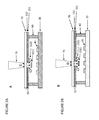
- FIG. 5 Show the schematic embodiment for interconnecting ball grid array type structures to a substrate
- FIG. 6 shows the schematic embodiment for the interconnection of a passive component or bare die on a foil
- FIG. 7 shows an example of a structured donor film.
- a direct write method for high speed positioning die bonding material for discrete chip components on substrates, which can be operated in a reel to reel manufacturing fashion.
- the method can be used for high resolution deposition of highly viscous materials. With the attainable resolution of the disclosed methods and systems, that a resolution spot size of transferred die bonding material may be attained with a spot diameter of the transferred bonding material that is smaller than 50 micron.
- FIG. 1 illustrates schematically several embodiments (A,B,C) of methods for bonding discrete pads 30 of a bare die chip components (chips) 10 on a pad structure 40 of flexible substrate 20 .
- the method has sufficient accuracy to correct for web deformations of the flexible substrate 20 .
- the term “flexible substrate” used in this text refers in particular to a substrate that is bendable enough to be used in a reel to reel process.
- a flexible substrate as used in this text is a substrate that is flexible enough to allow bending over a certain curvature, e.g. with a radius of 1-100 centimeters (depending on the reel diameter), without the substrate losing essential functionality.
- Supply of chip bonding material matter 50 can be placed on the pad structure 40 ( FIG.
- FIG. 1A a composite pattern of conductive die bonding matter and structural adhesive 60 may be provided ( FIG. 1C ). Also, alternatively, the method can be provided for interconnecting pad structures arranged on laminated flexible substrates.
- FIGS. 2A and 2B show exemplary transfer setups for transferring die bonding matter 1511 to a pad structure 40 on a substrate 20 ( Figure A) or to pads 30 of bare the 10 ( FIG. 2B ) for the method as presently claimed.
- a bonding method of a micro-electronic, in particular, a bare die component 10 is provided having one or more electrical connection pads, on a substrate 20 having on its substrate surface a connection pad structure 40 arranged for interconnecting the micro-electronic component via a respective one or more connection pads, the method comprising the steps of:
- a bonding method of a micro-electronic, in particular, a bare the component 10 is provided having one or more electrical connection pads, on a substrate 20 having on its substrate surface a connection pad structure 40 arranged for interconnecting the micro-electronic component via a respective one or more connection pads, the method comprising the steps of:
- the embodiments have as common concept that they provide for high speed high resolution bonding of micro-electronic components after placement thereof with their pads to respective pad structures of the substrate. Since the transferred adhesive or solder paste respectively remains intact, in particular, curable, or reflowable, during transfer, i.e. before placement, the bonding properties are optimal, so that after placement of the component 10 on the pad structure, the bonding matter, in particular, the adhesive or solder paste can be cured or reflowed respectively, to provide a robust bonding with electrical connectivity, that may have a bonding strength of more than 1 Mpa. This is a method that can be very efficient and cost effective for large scale industry purposes.
- a transparent carrier substrate 70 in the example, a quartz glass for a 248 nm KrF excimer and PET or Soda Lime Glass for a 355 nm Nd:YAG laser.
- a conductive die attach die bonding material 15 is provided comprising a die bonding material layer 151 of a conductive thermosetting material or flux based solder paste and a dynamic release layer 152 adjacent to the conductive thermosetting or flux based solder material die bonding material layer 151 .
- Dynamic release layers are well known in the art and typically comprise a composition formed in a layer, that abruptly locally transforms in gaseous substance, when locally irradiated so that dynamic release is provided by propulsion of the gaseous substance.
- the dynamic release layer 152 is formed by a Triazene layer of about 100 nm thickness which functions as a sacrificial dynamic release layer (DRL), and comprises a polymer that, when photoactivated decomposes into nitrogen and other organic volatile gases 1521 .
- DRL sacrificial dynamic release layer
- Other compositions to the effect that a dynamic release is provided of the substance provided on the dynamic release layer 152 i.e. dynamic release of bonding material of a curable conductive adhesive or flux based solder paste from the dynamic release layer 152 to a selected part of the connection pad structure 40 may be equally suitable.
- a typical peak absorption is found at 290-330 nm and the ablation threshold: 22-32 mJ/cm 2 at 308-248 nm is quite low so that the donor die attach film layer or solder paste is not thermally loaded and remains intact after transfer, in such a way that the the bonding matter 1511 remains thermosettable.
- the laser beam may be restricted in timing and energy, in such a way that bonding matter, transferred by dynamic release from the dynamic release layer 152 to the selected part of the connection pad or connection pad structure 40 remains curable or consists of more than 10% volume percent of solder flux.
- a desired material property can be retained during transfer from the dynamic release layer 152 to the pad structure by impinging the laser beam on the dynamic release layer 152 adjacent to the conductive thermosettable material of die bonding material layer 15 ; in such a way that the dynamic release layer 152 is activated to direct the conductive die attach die bonding matter 1511 to cover a selected part of the substrate 20 with transferred conductive die bonding material.
- thermosettable isotropic conductive adhesive material 151 is transferred, as can be seen by in the FIGS. 2 a and 2 b . having electrical conductivity on for instance coated Cu substrates or silver tracks with a volume resistivity of typically 4-10 E-4 Ohm ⁇ cm and a typical curing temperature of 10 to 3 min @ 120-150° C., commercially available as CE 3103 WLV from Henkel, with a viscosity of 15-25 Pa ⁇ s.
- Another experimental conductive adhesive from Henkel is transferred consisting of a highly viscous conductive adhesive with a viscosity of 160-180 Pa ⁇ s that is cured in around 10 min at 150° C.
- the conductive adhesive 151 is provided as homogenous layer of 20-30 micron, in particular, 25 micron thick provided on the dynamic release layer 152 .
- the thickness is controlled to be around 25 um or 50 um but could be theoretically be of any thickness.
- the donor bonding materials are held at a distance of about 13-150 micron away from the substrate by shims 80 .
- the conductive adhesive may also be replaced by a flux based Sn96.5Ag3Cu0.5 type 5 solder paste. Proper transfer of the solder with the flux can be achieved and functionality may be confirmed by reflow. Also nonconductive structural adhesives or pressure sensitive adhesives may be transferred successfully.
- the adhesive may have a viscosity of 1.2 Pa ⁇ s.
- a die bonding material layer may be a 15-30 micron thick solid thermoplastic layer with a high conductivity of about 7E-4 Ohm ⁇ cm and a curing schedule of about 1.5 h @ 175-200° C.
- FIGS. 3A and 3B transfer systems are illustrated for transferring conductive thermosettable adhesives or solder paste from a tape 70 on a reel 185 and wound back to a reel 180 .
- the bonding method as disclosed herein is adaptive and enables in combination with an alignment detection system accurate and adaptable corrections that renders it suitable for placement on a flexible foil wherein web integrity typically cannot be guaranteed.
- tape 70 can be made from PET foil and is passed through a donor feed system 75 where it is aligned under the beam of a laser 195 and transferred to pad structures 40 of an acceptor substrate 20 .
- the substrate can be moved by a motorized stage 190 that can be moved in accordance with alignment control means that align the substrate 20 relative to the laser 195 .
- FIG. 3B show another example wherein a donor film 15 is moved by a motorized stage 220 having respective guides 210 and 215 for guiding the film in an X-Y fashion over a substrate 20 .
- the substrate may be moving in a transport direction P by stage 220 .
- the laser 195 may be moved mechanically or optically, so that the transfer of bonding matter 1511 can be aligned relative to the substrate 20 .
- FIG. 4 shows a schematic assembly process for a micro-electronic component 10 that includes transferring chip bonding and interconnect matter by the LIFT method in transfer section 250 as illustrated in the preceding.
- a bare chip component interconnection method is disclosed for the interconnecting and bonding a bare chip component 10 on a flexible substrate or foil 20 with conductive die attach matter 50 and nonconductive die attach matter 60 .
- the method involves providing a flexible substrate 20 with contacts 40 and providing a bare chip component 10 with contacts 30 to be placed on a predefined placement by positioning means 255 .
- the method involves a thermal exposure step 260 where the chip is permanently fixed by curing the conductive thermoset or reflowing solder melt 280 and optionally the thermoset nonconductive adhesive 285 before the flexible substrate said foil is wound back onto the reel 270 .
- a substrate 20 or carrier web is unwound from a first reel 265 and guided via a set of guide rollers 240 to a second reel 270 to be wound up.
- various sub processes can be carried out, in particular, as one of the sub processes, bare chip component bonding as currently disclosed in the previous FIGS. 1 and 2 .
- these sub processes may involve:
- the chips 10 may be secured permanently to the substrate at the placement position e.g. by a bonding tool 260 such as a heater that activates the thermosetting material in the electrically conductive die bonding donor material that is thermosetting in a curing temperature region with a temperature elevated from the LIFT operating temperature in 260 so that the component is fixed by thermal curing, or any other known method for attaching chips to a (flexible) substrate.
- a bonding tool 260 such as a heater that activates the thermosetting material in the electrically conductive die bonding donor material that is thermosetting in a curing temperature region with a temperature elevated from the LIFT operating temperature in 260 so that the component is fixed by thermal curing, or any other known method for attaching chips to a (flexible) substrate.
- the bump array consists of bumps 40 on a substrate 20 with diameters typically in the range of 10 to 500 micron.
- the density is preferably such that a sufficient number of bumps 30 are under a chip 10 to be placed. e.g. if the chip is of 1 mm edge length for instance a distance of 200 microns may be still sufficient (5 bumps ⁇ 5 bumps under the chip).
- Solder paste or thermosettable adhesive 50 bumps may be placed onto the bond pads or onto the substrate pads and subsequently the bump array 30 of the chip 10 may be placed and bonded onto the substrate by e.g. a flip chip method.
- structural adhesive 60 may be transferred for further structural bonding.
- microelectronic components such as passive components e.g. resistors, capacitors or inductors 310 or bare die LED's 410 may be placed on a prepatterned foil 20 , wherein conductive adhesive or solder paste 50 and nonconductive adhesive 60 is applied by means of the above illustrated technique.
- Both the resistor 310 or bare die LED 410 are to be connected in the current example with the substrate foil 20 through conductive bumps to conductive tracks 40 .
- circuits are advantageously applied on a flexible substrate to be applied e.g. on silver or copper tracks on PEN or PET foils.
- a typical chip height may vary e.g. between 0-250 micrometers.
- the bare the LED 410 has an anode bump 425 and cathode bump 426 of about 80 ⁇ 80 micron or even smaller to about 50 ⁇ 50 micron, and a junction area 415 (LED part) of about 230 ⁇ 190 micron.
- the deposition step can be carried out as one embodiment of a method of treatment of bumps for chip dies in a chip manufacturing process.
- the method comprises clamping a wafer having identified bumps to be provided with a conductive adhesive; providing a conductive die attach donor film distanced from the wafer top surface; aligning the laser beam of the laser system and guiding the conductive the attach donor film relative to an identified bump on the wafer; and impinging a laser beam on a side of the conductive die attach donor film opposite a side facing the wafer; the laser beam tuned in timing, energy and direction to generate conductive die attach donor film matter directed towards a bump to be treated.
- a further embodiment involves a multishot process repeated steps are provided of guiding fresh conductive the attach donor film relative to the bump and impinging the laser beam on the conductive die attach donor film so as to direct a particle of conductive the bonding matter onto the bump.
- a laser repetition rate is preferably at least 60-600 kHz.
- a conductive the attach donor film refreshment module with high refresh rate capabilities is very advantageous, for example having a conductive the attach donor film refreshment velocity relative to the bump of more than 0.1 m/s.
- the high laser repetition rate combined with a relative high number of about 60-200 of bumps provides an effective operation range for this chip bonding application competitive with stencil or screen printing and far superior to the deposition rate to that of jet printing with approx. 10 bumps per second.
- FIG. 7 shows an example of a structured donor film 70 .
- the donor film may be provided in a premachined form, for example, comprising a sacrificial layer, a prepatterned conductive the bonding material layer provided in a matrix 15 of sacrificial material.
- a suitable thickness of the homogenous layer may range between 50 and 2000 nm, preferably in a range of 50-500 nm or even more preferably in a range of 50-250 nm.
- an embodiment for treatment of a bump can be carried out by stepping i.e. a non-roll to roll process.
- a fast beam modulator galvano mirror, polygon mirror, acousto-optic or electro-optic modulator etc.
- the modulator may be controlled in a feed forward process wherein bump coordinates are provided from an external source that provides the layout data of a chip die.
- the modulator can be used as a scanning unit that maps the bump coordinates in a prescan stage.
- an additional optical feedback system may provide laser alignment relative to the bump.
- a main beam is split into about 2-20 sub beams.
- each single bump may be treated by a multishot process where repeated steps are provided of guiding fresh conductive die attach the bonding material relative to the bump and generating a donor matter.
- the advantage of the disclosed laser transfer process over conventional printing is the range of use: for the intended features with a resolution ⁇ 50 ⁇ m stencil printing techniques generally fail (resolution spot size typically 75 ⁇ m) and jet printing even more (typical resolution spot size: 200 ⁇ m).
- the donor matter may have a wide-range of viscosity, possible to transfer (from 1 Pa ⁇ s to 160 Pa ⁇ s (non-exhaustive)).
- For stencil printing typical viscosities are >50 Pa ⁇ s and for Inkjet printing typical viscosities are ⁇ 0.1 Pa ⁇ s. Contrary to stencil printing and screen printing it is a non-contact direct write method with the possibility of on the fly correction for web deformations using a vision system.
Abstract
Description
-
- providing a donor film comprising a bonding material of a curable conductive adhesive or flux based solder paste and a dynamic release layer adjacent to the bonding material layer;
- aligning a laser beam of a laser system and guiding the donor film distanced from the substrate surface;
- impinging the laser beam on the dynamic release layer; in such a way that the dynamic release layer is activated to cover a selected part of the connection pads or the connection pad structure with bonding matter transferred from the bonding material layer; and
- administering the micro-electronic component with its pads to the pad structure, so that the bonding matter on one or both the pads and the pad structure forms an electrical connection between the pad structure and a respective pad; and
- bonding the micro-electronic component with a shear strength of more than 1 Mpa, by curing the conductive adhesive or reflowing the solder paste of the bonding matter.
-
- providing a donor film comprising a curable conductive adhesive 151 and a
dynamic release layer 152; - aligning a laser beam of a laser system and guiding the donor film distanced from the substrate surface;
- impinging the laser beam on the dynamic release layer; in such a way that the dynamic release layer is activated to cover a selected part of the connection pads or the connection pad structure with adhesive 50 transferred from the donor film; wherein the laser beam is restricted in timing and energy, in such a way that the transferred adhesive remains curable;
- administering the
micro-electronic component 10 with its pads to the pad structure, so that the bonding matter on one or both the pads and the pad structure forms an electrical connection between the pad structure and a respective pad; and - curing the conductive adhesive between the pads and the pad structure to bond the micro-electronic component with a shear strength of more than 1 Mpa.
- providing a donor film comprising a curable conductive adhesive 151 and a
-
- providing a donor film comprising a
solder paste 151 and adynamic release layer 152; - aligning a laser beam of a laser system and guiding the donor film distanced from the substrate surface;
- impinging the laser beam on the dynamic release layer; in such a way that the dynamic release layer is activated to cover a selected part of the connection pads or the connection pad structure with
solder paste 50 transferred from the donor film; wherein the laser beam is restricted in timing and energy, in such a way that the transferred solder paste includes flux consisting of more than 10% volume percent of flux; - administering the
micro-electronic component 10 with its pads to the pad structure, so that the solder paste on one or both the pads and the pad structure forms an electrical connection between the pad structure and a respective pad; and - reflowing the solder paste between the pads and the pad structure to bond the micro-electronic component with a shear strength of more than 1 Mpa.
- providing a donor film comprising a
-
- making 250 interconnects by LIFT transfer process directing conductive and nonconductive die
bonding matter 60 to acceptor - supply of a
bare chip component 10, for example, a silicon based bare chip component orLED 10, to the target area on thesubstrate 20 by a pick andplace unit 255 onto the interconnect material and controlling the pressure; - fixing of the
die chip component 10 by athermal curing unit 260 by thermosetting of the conductive and non-conductive adhesive 60 and/or reflow of the solder paste.
- making 250 interconnects by LIFT transfer process directing conductive and nonconductive die
Claims (14)
Applications Claiming Priority (4)
| Application Number | Priority Date | Filing Date | Title |
|---|---|---|---|
| EP12192091.2 | 2012-11-09 | ||
| EP12192091.2A EP2731126A1 (en) | 2012-11-09 | 2012-11-09 | Method for bonding bare chip dies |
| EP12192091 | 2012-11-09 | ||
| PCT/NL2013/050800 WO2014073963A1 (en) | 2012-11-09 | 2013-11-08 | Method for bonding bare chip dies |
Publications (2)
| Publication Number | Publication Date |
|---|---|
| US20150294951A1 US20150294951A1 (en) | 2015-10-15 |
| US9859247B2 true US9859247B2 (en) | 2018-01-02 |
Family
ID=47216108
Family Applications (1)
| Application Number | Title | Priority Date | Filing Date |
|---|---|---|---|
| US14/441,714 Active 2033-12-11 US9859247B2 (en) | 2012-11-09 | 2013-11-08 | Method for bonding bare chip dies |
Country Status (7)
| Country | Link |
|---|---|
| US (1) | US9859247B2 (en) |
| EP (2) | EP2731126A1 (en) |
| JP (1) | JP6283679B2 (en) |
| KR (1) | KR102160321B1 (en) |
| CN (1) | CN104854686B (en) |
| TW (1) | TWI674654B (en) |
| WO (1) | WO2014073963A1 (en) |
Cited By (3)
| Publication number | Priority date | Publication date | Assignee | Title |
|---|---|---|---|---|
| US20180193948A1 (en) * | 2015-07-09 | 2018-07-12 | Orbotech Ltd. | Control of Lift Ejection Angle |
| US20210292909A1 (en) * | 2016-11-23 | 2021-09-23 | Institut National De La Recherche Scientifique | System for laser-driven impact acceleration |
| US20220248540A1 (en) * | 2021-01-29 | 2022-08-04 | Orbotech Ltd. | High-resolution soldering |
Families Citing this family (23)
| Publication number | Priority date | Publication date | Assignee | Title |
|---|---|---|---|---|
| ES2471568B1 (en) * | 2012-11-22 | 2015-08-21 | Abengoa Solar New Technologies S.A. | Procedure for creating electrical contacts and contacts thus created |
| TWI561325B (en) * | 2014-08-01 | 2016-12-11 | Au Optronics Corp | Display module manufacturing method and display module |
| CN106716611B (en) | 2014-10-17 | 2019-08-20 | 英特尔公司 | Micro- pickup and bonding assembling |
| DE102016103324A1 (en) * | 2016-02-25 | 2017-08-31 | Osram Opto Semiconductors Gmbh | Video wall module and method of making a video wall module |
| US9916989B2 (en) | 2016-04-15 | 2018-03-13 | Amkor Technology, Inc. | System and method for laser assisted bonding of semiconductor die |
| WO2017188125A1 (en) * | 2016-04-27 | 2017-11-02 | セイコーエプソン株式会社 | Mounting structure, ultrasonic device, ultrasonic probe, ultrasonic apparatus, and electronic equipment |
| US10032827B2 (en) * | 2016-06-29 | 2018-07-24 | Applied Materials, Inc. | Systems and methods for transfer of micro-devices |
| CN108346640B (en) * | 2017-01-25 | 2020-02-07 | 华邦电子股份有限公司 | Semiconductor structure and manufacturing method thereof |
| JP6720333B2 (en) | 2017-06-12 | 2020-07-08 | ユニカルタ・インコーポレイテッド | How to assemble individual components in parallel on a board |
| US11201077B2 (en) | 2017-06-12 | 2021-12-14 | Kulicke & Soffa Netherlands B.V. | Parallel assembly of discrete components onto a substrate |
| CN110546771B (en) * | 2017-06-15 | 2022-04-08 | 歌尔股份有限公司 | Micro light emitting diode transfer method, micro light emitting diode device and electronic equipment |
| US10163773B1 (en) | 2017-08-11 | 2018-12-25 | General Electric Company | Electronics package having a self-aligning interconnect assembly and method of making same |
| CN109994413A (en) * | 2017-12-29 | 2019-07-09 | 南昌欧菲显示科技有限公司 | Micro element flood tide transfer method |
| TWI688317B (en) * | 2018-10-31 | 2020-03-11 | 台灣愛司帝科技股份有限公司 | Led mounted method and device |
| CN113690149A (en) * | 2020-05-16 | 2021-11-23 | 佛山市国星光电股份有限公司 | Chip bonding structure, method and equipment |
| KR20230021667A (en) | 2020-06-04 | 2023-02-14 | 오르보테크 엘티디. | high resolution soldering |
| CN113451274B (en) * | 2020-10-28 | 2022-08-05 | 重庆康佳光电技术研究院有限公司 | LED chip assembly, display panel and preparation method |
| US11631650B2 (en) * | 2021-06-15 | 2023-04-18 | International Business Machines Corporation | Solder transfer integrated circuit packaging |
| DE102021119155A1 (en) * | 2021-07-23 | 2023-01-26 | OSRAM Opto Semiconductors Gesellschaft mit beschränkter Haftung | METHOD OF APPLYING AN ELECTRICAL JOINT OR FLUX TO A COMPONENT |
| TW202343603A (en) * | 2022-02-18 | 2023-11-01 | 日商迪睿合股份有限公司 | Method for manufacturing connection structure and method for transfer individualized adhesive film |
| EP4276889A1 (en) | 2022-05-12 | 2023-11-15 | STMicroelectronics S.r.l. | Method of manufacturing a semiconductor device and the corresponding semiconductor device |
| CN115579440B (en) * | 2022-12-09 | 2023-07-18 | 惠科股份有限公司 | LED chip, brushing device and brushing die bonding method of LED chip |
| CN116364561B (en) * | 2023-06-01 | 2023-09-08 | 湖北三维半导体集成创新中心有限责任公司 | Bonding method and bonding structure |
Citations (68)
| Publication number | Priority date | Publication date | Assignee | Title |
|---|---|---|---|---|
| US3560258A (en) | 1966-07-22 | 1971-02-02 | Int Standard Electric Corp | Pattern deposit by laser |
| US4752455A (en) | 1986-05-27 | 1988-06-21 | Kms Fusion, Inc. | Pulsed laser microfabrication |
| US4987006A (en) | 1990-03-26 | 1991-01-22 | Amp Incorporated | Laser transfer deposition |
| EP0643153A1 (en) | 1993-09-09 | 1995-03-15 | KRONE Aktiengesellschaft | Process for the fabrication of structured metallizations on surfaces |
| JPH0837206A (en) | 1994-07-22 | 1996-02-06 | Nec Corp | Method of manufacturing semiconductor device |
| US5593808A (en) | 1993-08-13 | 1997-01-14 | Rexham Graphics Inc. | LAT imaging onto intermediate/receptor elements/"LAT decalcomania" |
| JPH09129649A (en) | 1995-11-06 | 1997-05-16 | Matsushita Electric Ind Co Ltd | Method of feeding and packaging junction material |
| WO1998005068A1 (en) | 1996-07-26 | 1998-02-05 | Philips Electronics N.V. | Method of manufacturing and transferring metallic droplets |
| JPH1070151A (en) | 1996-08-26 | 1998-03-10 | Ricoh Co Ltd | Method and apparatus for arraying conductive particle |
| WO1998050189A1 (en) | 1997-05-08 | 1998-11-12 | Shapiro Herbert M | Apparatus and method for forming solder bonding pads |
| US6060127A (en) | 1998-03-31 | 2000-05-09 | Matsushita Electric Industrial Co., Ltd. | Mechanically restricted laser deposition |
| US6159832A (en) | 1998-03-18 | 2000-12-12 | Mayer; Frederick J. | Precision laser metallization |
| DE19946182A1 (en) | 1999-09-21 | 2001-03-29 | Forschungsverbund Berlin Ev | Production of carbon nanotubes used in microelectronics comprises focussing laser pulses onto surface of carbon-containing material, vaporizing and decomposing carbon-containing molecules and growing carbon nanotubes |
| JP2001237279A (en) | 2000-02-23 | 2001-08-31 | Hitachi Ltd | Semiconductor device and electronic apparatus comprising it |
| US20020071901A1 (en) | 1999-01-27 | 2002-06-13 | Ringeisen Bradley R. | Generation of biomaterial microarrays by laser transfer |
| US20020081397A1 (en) | 1999-01-27 | 2002-06-27 | Mcgill R. Andrew | Fabrication of conductive/non-conductive nanocomposites by laser evaporation |
| US20030087476A1 (en) | 2001-09-06 | 2003-05-08 | Toyoharu Oohata | Method of transferring devices, method of arranging devices using the same, and method of manufacturing an image display system |
| WO2003054630A2 (en) | 2001-12-21 | 2003-07-03 | Austria Wirtschaftsservice Gesellschaft mit beschränkter Haftung | Device and method for modifying the surface of a workpiece using photonic radiation |
| WO2003056320A2 (en) | 2001-12-28 | 2003-07-10 | Foundation For Research And Technology Hellas (F.O.R.T.H) | Fabrication of biopolymer patterns by means of laser transfer |
| US20030180638A1 (en) | 2002-03-13 | 2003-09-25 | Eastman Kodak Company | Transfer of organic material from a donor to form a layer in an oled device |
| US20030178395A1 (en) | 2000-05-24 | 2003-09-25 | Duignan Michael T. | Method and apparatus for fabrication of miniature structures |
| WO2003101165A1 (en) | 2000-07-20 | 2003-12-04 | The United States Of America As Represented By The Secretary Of The Navy | Direct-write laser transfer and processing |
| US20040022947A1 (en) | 2002-08-01 | 2004-02-05 | Duignan Michael T. | Method for creating microstructure patterns by contact transfer technique |
| US20040029039A1 (en) | 2002-08-02 | 2004-02-12 | Eastman Kodak Company | Laser thermal transfer donor including a separate dopant layer |
| US20040033433A1 (en) | 1989-03-30 | 2004-02-19 | Foley Diane M. | Novel ablation-transfer imaging/recording |
| DE10237732A1 (en) | 2002-08-17 | 2004-03-18 | BLZ Bayerisches Laserzentrum Gemeinnützige Forschungsgesellschaft mbH | Laser marking by transferring marking material from carrier to surface includes second radiation phase to attach material to surface |
| US6792326B1 (en) | 1999-05-24 | 2004-09-14 | Potomac Photonics, Inc. | Material delivery system for miniature structure fabrication |
| US20040247777A1 (en) | 2003-06-06 | 2004-12-09 | Ringeisen Bradley R. | Biological laser printing for tissue microdissection via indirect photon-biomaterial interactions |
| US20040250769A1 (en) | 2002-10-28 | 2004-12-16 | Finisar Corporation | Pulsed laser deposition for mass production |
| US20050054121A1 (en) | 2003-09-05 | 2005-03-10 | Handy Erik S. | Laser transfer article and method of making |
| US20050085385A1 (en) | 2003-10-20 | 2005-04-21 | Swihart Donald L. | Laser-generated ultraviolet radiation mask |
| US20050266152A1 (en) | 2004-05-27 | 2005-12-01 | Eastman Kodak Company | Depositing an organic layer for use in OLEDs |
| US20060007397A1 (en) | 2004-06-30 | 2006-01-12 | Lai Shui T | Apparatus and method for determining sphere and cylinder components of subjective refraction using objective wavefront measurement |
| US20060035454A1 (en) | 2004-08-16 | 2006-02-16 | Ibm Corporation | Fluxless solder transfer and reflow process |
| US7001467B2 (en) | 1999-07-19 | 2006-02-21 | The United States Of America As Represented By The Secretary Of The Navy | Direct-write laser transfer and processing |
| US20060213886A1 (en) | 2003-03-13 | 2006-09-28 | Sanders Renatus H M | Marking method and market object |
| US20060234163A1 (en) | 2005-04-13 | 2006-10-19 | Lei Zhu | Laser-assisted deposition |
| WO2007071985A1 (en) | 2005-12-20 | 2007-06-28 | The University Of Bristol | Method of and apparatus for transferring material from a carrier to a substrate by laser irradiation |
| US20070180991A1 (en) | 2003-07-29 | 2007-08-09 | Anand Chellappa | Methods for providing thin hydrogen seperation membranes and associated uses |
| US7348270B1 (en) | 2007-01-22 | 2008-03-25 | International Business Machines Corporation | Techniques for forming interconnects |
| US20080108171A1 (en) | 2006-09-20 | 2008-05-08 | Rogers John A | Release strategies for making transferable semiconductor structures, devices and device components |
| US20080139075A1 (en) | 2006-05-12 | 2008-06-12 | Photon Dynamics, Inc. | Deposition Repair Apparatus And Methods |
| US20080299496A1 (en) | 2007-06-01 | 2008-12-04 | Semiconductor Energy Laboratory Co., Ltd. | Manufacturing Apparatus and Manufacturing Method of Light-Emitting Device |
| US20080314881A1 (en) | 2007-06-19 | 2008-12-25 | The Government Of The United States Of America, As Represented By The Secretary Of The Navy | Sub-micron laser direct write |
| US20090074987A1 (en) | 2007-09-14 | 2009-03-19 | Photon Dynamics, Inc. | Laser decal transfer of electronic materials |
| US20090104403A1 (en) | 2007-10-23 | 2009-04-23 | Semiconductror Energy Laboratory Co., Ltd. | Evaporation Donor Substrate and Method for Manufacturing Light-Emitting Device |
| US20090130427A1 (en) | 2007-10-22 | 2009-05-21 | The Regents Of The University Of California | Nanomaterial facilitated laser transfer |
| US20090130467A1 (en) | 2007-11-21 | 2009-05-21 | Industrial Technology Research Institute | Transfer component and laser-assisted transfer system using the same |
| WO2009081355A2 (en) | 2007-12-19 | 2009-07-02 | Koninklijke Philips Electronics N.V. | Optical disk format for direct writing materials on a substrate |
| US20090169809A1 (en) | 2007-12-26 | 2009-07-02 | Semiconductor Energy Laboratory Co., Ltd. | Evaporation Donor Substrate, Method for Manufacturing the Same, and Method for Manufacturing Light-Emitting Device |
| WO2009090098A2 (en) | 2008-01-17 | 2009-07-23 | Schmid Technology Gmbh | Method and apparatus for producing a solar cell |
| US20090217517A1 (en) | 2008-02-20 | 2009-09-03 | The United Sates Of America As Represented By The Secretary Of The Navy | Laser-based technique for the transfer and embedding of electronic components and devices |
| US20090226637A1 (en) | 2008-03-07 | 2009-09-10 | Semiconductor Energy Laboratory Co., Ltd. | Deposition Method and Method for Manufacturing Light-Emitting Device |
| US20090305445A1 (en) | 2008-06-04 | 2009-12-10 | Semiconductor Energy Laboratories, Co., Ltd. | Method for Manufacturing Light-Emitting Device |
| WO2009146680A1 (en) | 2008-06-04 | 2009-12-10 | Universität Zu Lübeck | Carrier system for the laser microdissection and the laser-induced transport of biological material and living cells |
| WO2009153792A2 (en) | 2008-06-19 | 2009-12-23 | Utilight Ltd. | Light induced patterning |
| US20100123258A1 (en) * | 2008-11-14 | 2010-05-20 | Myung Jin Yim | Low Temperature Board Level Assembly Using Anisotropically Conductive Materials |
| US20100227133A1 (en) | 2009-03-09 | 2010-09-09 | Imra America, Inc. | Pulsed laser micro-deposition pattern formation |
| US20110003440A1 (en) | 2009-03-31 | 2011-01-06 | Infineon Technologies Ag | Method of manufacturing a semiconductor device |
| WO2011009973A2 (en) | 2009-07-22 | 2011-01-27 | Universidad De Barcelona | Apparatus and method for direct laser printing |
| WO2011032938A1 (en) | 2009-09-15 | 2011-03-24 | Von Ardenne Anlagentechnik Gmbh | Method and device for locally depositing a material on a substrate |
| US20110089412A1 (en) | 2008-06-16 | 2011-04-21 | Shigeo Fujimori | Patterning method, production method of device using the patterning method, and device |
| WO2011107599A1 (en) | 2010-03-04 | 2011-09-09 | INSERM (Institut National de la Santé et de la Recherche Médicale) | Bioprinting station, assembly comprising such bioprinting station and bioprinting method |
| WO2011123285A1 (en) | 2010-03-29 | 2011-10-06 | Semprius, Inc. | Selective transfer of active components |
| US20110278566A1 (en) | 2010-05-17 | 2011-11-17 | Industry-Academic Cooperation Foundation, Yonsei University | Method of patterning thin film solution-deposited |
| WO2011154747A1 (en) | 2010-06-11 | 2011-12-15 | Dzp Technologies Limited | Method and apparatus for deposition |
| WO2012019882A1 (en) | 2010-08-10 | 2012-02-16 | Von Ardenne Anlagentechnik Gmbh | Method and use of a device for producing a layer of an organic material on a substrate |
| EP2487215A1 (en) | 2011-02-11 | 2012-08-15 | Henkel AG & Co. KGaA | Electrically conductive adhesives comprising at least one metal precursor |
Family Cites Families (1)
| Publication number | Priority date | Publication date | Assignee | Title |
|---|---|---|---|---|
| US5685939A (en) * | 1995-03-10 | 1997-11-11 | Minnesota Mining And Manufacturing Company | Process for making a Z-axis adhesive and establishing electrical interconnection therewith |
-
2012
- 2012-11-09 EP EP12192091.2A patent/EP2731126A1/en not_active Withdrawn
-
2013
- 2013-11-08 KR KR1020157015349A patent/KR102160321B1/en active IP Right Grant
- 2013-11-08 TW TW102140687A patent/TWI674654B/en active
- 2013-11-08 EP EP13801876.7A patent/EP2917931B1/en active Active
- 2013-11-08 JP JP2015541717A patent/JP6283679B2/en active Active
- 2013-11-08 WO PCT/NL2013/050800 patent/WO2014073963A1/en active Application Filing
- 2013-11-08 CN CN201380065264.9A patent/CN104854686B/en active Active
- 2013-11-08 US US14/441,714 patent/US9859247B2/en active Active
Patent Citations (71)
| Publication number | Priority date | Publication date | Assignee | Title |
|---|---|---|---|---|
| US3560258A (en) | 1966-07-22 | 1971-02-02 | Int Standard Electric Corp | Pattern deposit by laser |
| US4752455A (en) | 1986-05-27 | 1988-06-21 | Kms Fusion, Inc. | Pulsed laser microfabrication |
| US20040033433A1 (en) | 1989-03-30 | 2004-02-19 | Foley Diane M. | Novel ablation-transfer imaging/recording |
| US4987006A (en) | 1990-03-26 | 1991-01-22 | Amp Incorporated | Laser transfer deposition |
| US5593808A (en) | 1993-08-13 | 1997-01-14 | Rexham Graphics Inc. | LAT imaging onto intermediate/receptor elements/"LAT decalcomania" |
| EP0643153A1 (en) | 1993-09-09 | 1995-03-15 | KRONE Aktiengesellschaft | Process for the fabrication of structured metallizations on surfaces |
| JPH0837206A (en) | 1994-07-22 | 1996-02-06 | Nec Corp | Method of manufacturing semiconductor device |
| JPH09129649A (en) | 1995-11-06 | 1997-05-16 | Matsushita Electric Ind Co Ltd | Method of feeding and packaging junction material |
| WO1998005068A1 (en) | 1996-07-26 | 1998-02-05 | Philips Electronics N.V. | Method of manufacturing and transferring metallic droplets |
| JPH1070151A (en) | 1996-08-26 | 1998-03-10 | Ricoh Co Ltd | Method and apparatus for arraying conductive particle |
| US5873511A (en) | 1997-05-08 | 1999-02-23 | Shapiro; Herbert M. | Apparatus and method for forming solder bonding pads |
| WO1998050189A1 (en) | 1997-05-08 | 1998-11-12 | Shapiro Herbert M | Apparatus and method for forming solder bonding pads |
| US6159832A (en) | 1998-03-18 | 2000-12-12 | Mayer; Frederick J. | Precision laser metallization |
| US6060127A (en) | 1998-03-31 | 2000-05-09 | Matsushita Electric Industrial Co., Ltd. | Mechanically restricted laser deposition |
| US20020081397A1 (en) | 1999-01-27 | 2002-06-27 | Mcgill R. Andrew | Fabrication of conductive/non-conductive nanocomposites by laser evaporation |
| US20020071901A1 (en) | 1999-01-27 | 2002-06-13 | Ringeisen Bradley R. | Generation of biomaterial microarrays by laser transfer |
| US6792326B1 (en) | 1999-05-24 | 2004-09-14 | Potomac Photonics, Inc. | Material delivery system for miniature structure fabrication |
| US7001467B2 (en) | 1999-07-19 | 2006-02-21 | The United States Of America As Represented By The Secretary Of The Navy | Direct-write laser transfer and processing |
| DE19946182A1 (en) | 1999-09-21 | 2001-03-29 | Forschungsverbund Berlin Ev | Production of carbon nanotubes used in microelectronics comprises focussing laser pulses onto surface of carbon-containing material, vaporizing and decomposing carbon-containing molecules and growing carbon nanotubes |
| JP2001237279A (en) | 2000-02-23 | 2001-08-31 | Hitachi Ltd | Semiconductor device and electronic apparatus comprising it |
| US20030178395A1 (en) | 2000-05-24 | 2003-09-25 | Duignan Michael T. | Method and apparatus for fabrication of miniature structures |
| WO2003101165A1 (en) | 2000-07-20 | 2003-12-04 | The United States Of America As Represented By The Secretary Of The Navy | Direct-write laser transfer and processing |
| US20030087476A1 (en) | 2001-09-06 | 2003-05-08 | Toyoharu Oohata | Method of transferring devices, method of arranging devices using the same, and method of manufacturing an image display system |
| WO2003054630A2 (en) | 2001-12-21 | 2003-07-03 | Austria Wirtschaftsservice Gesellschaft mit beschränkter Haftung | Device and method for modifying the surface of a workpiece using photonic radiation |
| WO2003056320A2 (en) | 2001-12-28 | 2003-07-10 | Foundation For Research And Technology Hellas (F.O.R.T.H) | Fabrication of biopolymer patterns by means of laser transfer |
| US20030180638A1 (en) | 2002-03-13 | 2003-09-25 | Eastman Kodak Company | Transfer of organic material from a donor to form a layer in an oled device |
| US20040022947A1 (en) | 2002-08-01 | 2004-02-05 | Duignan Michael T. | Method for creating microstructure patterns by contact transfer technique |
| US20040029039A1 (en) | 2002-08-02 | 2004-02-12 | Eastman Kodak Company | Laser thermal transfer donor including a separate dopant layer |
| DE10237732A1 (en) | 2002-08-17 | 2004-03-18 | BLZ Bayerisches Laserzentrum Gemeinnützige Forschungsgesellschaft mbH | Laser marking by transferring marking material from carrier to surface includes second radiation phase to attach material to surface |
| US20040250769A1 (en) | 2002-10-28 | 2004-12-16 | Finisar Corporation | Pulsed laser deposition for mass production |
| US20060213886A1 (en) | 2003-03-13 | 2006-09-28 | Sanders Renatus H M | Marking method and market object |
| US20040247777A1 (en) | 2003-06-06 | 2004-12-09 | Ringeisen Bradley R. | Biological laser printing for tissue microdissection via indirect photon-biomaterial interactions |
| US20070180991A1 (en) | 2003-07-29 | 2007-08-09 | Anand Chellappa | Methods for providing thin hydrogen seperation membranes and associated uses |
| US20050054121A1 (en) | 2003-09-05 | 2005-03-10 | Handy Erik S. | Laser transfer article and method of making |
| US20050085385A1 (en) | 2003-10-20 | 2005-04-21 | Swihart Donald L. | Laser-generated ultraviolet radiation mask |
| US20050266152A1 (en) | 2004-05-27 | 2005-12-01 | Eastman Kodak Company | Depositing an organic layer for use in OLEDs |
| US20060007397A1 (en) | 2004-06-30 | 2006-01-12 | Lai Shui T | Apparatus and method for determining sphere and cylinder components of subjective refraction using objective wavefront measurement |
| US20060035454A1 (en) | 2004-08-16 | 2006-02-16 | Ibm Corporation | Fluxless solder transfer and reflow process |
| US20060234163A1 (en) | 2005-04-13 | 2006-10-19 | Lei Zhu | Laser-assisted deposition |
| WO2007071985A1 (en) | 2005-12-20 | 2007-06-28 | The University Of Bristol | Method of and apparatus for transferring material from a carrier to a substrate by laser irradiation |
| US20080139075A1 (en) | 2006-05-12 | 2008-06-12 | Photon Dynamics, Inc. | Deposition Repair Apparatus And Methods |
| US20080108171A1 (en) | 2006-09-20 | 2008-05-08 | Rogers John A | Release strategies for making transferable semiconductor structures, devices and device components |
| US7348270B1 (en) | 2007-01-22 | 2008-03-25 | International Business Machines Corporation | Techniques for forming interconnects |
| US20080299496A1 (en) | 2007-06-01 | 2008-12-04 | Semiconductor Energy Laboratory Co., Ltd. | Manufacturing Apparatus and Manufacturing Method of Light-Emitting Device |
| US20080314881A1 (en) | 2007-06-19 | 2008-12-25 | The Government Of The United States Of America, As Represented By The Secretary Of The Navy | Sub-micron laser direct write |
| US20090074987A1 (en) | 2007-09-14 | 2009-03-19 | Photon Dynamics, Inc. | Laser decal transfer of electronic materials |
| US20090130427A1 (en) | 2007-10-22 | 2009-05-21 | The Regents Of The University Of California | Nanomaterial facilitated laser transfer |
| US20090104403A1 (en) | 2007-10-23 | 2009-04-23 | Semiconductror Energy Laboratory Co., Ltd. | Evaporation Donor Substrate and Method for Manufacturing Light-Emitting Device |
| US20090130467A1 (en) | 2007-11-21 | 2009-05-21 | Industrial Technology Research Institute | Transfer component and laser-assisted transfer system using the same |
| WO2009081355A2 (en) | 2007-12-19 | 2009-07-02 | Koninklijke Philips Electronics N.V. | Optical disk format for direct writing materials on a substrate |
| US20090169809A1 (en) | 2007-12-26 | 2009-07-02 | Semiconductor Energy Laboratory Co., Ltd. | Evaporation Donor Substrate, Method for Manufacturing the Same, and Method for Manufacturing Light-Emitting Device |
| WO2009090098A2 (en) | 2008-01-17 | 2009-07-23 | Schmid Technology Gmbh | Method and apparatus for producing a solar cell |
| US20090217517A1 (en) | 2008-02-20 | 2009-09-03 | The United Sates Of America As Represented By The Secretary Of The Navy | Laser-based technique for the transfer and embedding of electronic components and devices |
| US20090226637A1 (en) | 2008-03-07 | 2009-09-10 | Semiconductor Energy Laboratory Co., Ltd. | Deposition Method and Method for Manufacturing Light-Emitting Device |
| WO2009146680A1 (en) | 2008-06-04 | 2009-12-10 | Universität Zu Lübeck | Carrier system for the laser microdissection and the laser-induced transport of biological material and living cells |
| US20090305445A1 (en) | 2008-06-04 | 2009-12-10 | Semiconductor Energy Laboratories, Co., Ltd. | Method for Manufacturing Light-Emitting Device |
| US20110089412A1 (en) | 2008-06-16 | 2011-04-21 | Shigeo Fujimori | Patterning method, production method of device using the patterning method, and device |
| WO2009153792A2 (en) | 2008-06-19 | 2009-12-23 | Utilight Ltd. | Light induced patterning |
| US20110097550A1 (en) | 2008-06-19 | 2011-04-28 | Utillight Ltd. | Light induced patterning |
| US20100123258A1 (en) * | 2008-11-14 | 2010-05-20 | Myung Jin Yim | Low Temperature Board Level Assembly Using Anisotropically Conductive Materials |
| US20100227133A1 (en) | 2009-03-09 | 2010-09-09 | Imra America, Inc. | Pulsed laser micro-deposition pattern formation |
| US20110003440A1 (en) | 2009-03-31 | 2011-01-06 | Infineon Technologies Ag | Method of manufacturing a semiconductor device |
| WO2011009973A2 (en) | 2009-07-22 | 2011-01-27 | Universidad De Barcelona | Apparatus and method for direct laser printing |
| WO2011032938A1 (en) | 2009-09-15 | 2011-03-24 | Von Ardenne Anlagentechnik Gmbh | Method and device for locally depositing a material on a substrate |
| WO2011107599A1 (en) | 2010-03-04 | 2011-09-09 | INSERM (Institut National de la Santé et de la Recherche Médicale) | Bioprinting station, assembly comprising such bioprinting station and bioprinting method |
| WO2011123285A1 (en) | 2010-03-29 | 2011-10-06 | Semprius, Inc. | Selective transfer of active components |
| US20110278566A1 (en) | 2010-05-17 | 2011-11-17 | Industry-Academic Cooperation Foundation, Yonsei University | Method of patterning thin film solution-deposited |
| WO2011154747A1 (en) | 2010-06-11 | 2011-12-15 | Dzp Technologies Limited | Method and apparatus for deposition |
| WO2012019882A1 (en) | 2010-08-10 | 2012-02-16 | Von Ardenne Anlagentechnik Gmbh | Method and use of a device for producing a layer of an organic material on a substrate |
| EP2487215A1 (en) | 2011-02-11 | 2012-08-15 | Henkel AG & Co. KGaA | Electrically conductive adhesives comprising at least one metal precursor |
| WO2012107556A2 (en) | 2011-02-11 | 2012-08-16 | Henkel Ag & Co. Kgaa | Electrically conductive adhesives comprising at least one metal precursor |
Non-Patent Citations (7)
| Title |
|---|
| Digital Microfabrication by Laser Decal Transfer, Pique et al, 2008. |
| International Search Report-PCT/NL2013/050800-dated Feb. 20, 2014. |
| International Search Report—PCT/NL2013/050800—dated Feb. 20, 2014. |
| Laser Decal Transfer of Electronic Materials with Thin Film Characteristics, Pique et al. |
| Laser printing of mutt-layered polymermetal heterostructures, Bimbaum et al, 2010. |
| Three Dimensional Printing of Interconnects by Laser Direct-Write of Silver Nanopastes by Jiwen Wang et al, 2010. |
| Triazene photopolymer dynamic release layer-assisted, Banks et al, 2008. |
Cited By (6)
| Publication number | Priority date | Publication date | Assignee | Title |
|---|---|---|---|---|
| US20180193948A1 (en) * | 2015-07-09 | 2018-07-12 | Orbotech Ltd. | Control of Lift Ejection Angle |
| US10471538B2 (en) * | 2015-07-09 | 2019-11-12 | Orbotech Ltd. | Control of lift ejection angle |
| US20210292909A1 (en) * | 2016-11-23 | 2021-09-23 | Institut National De La Recherche Scientifique | System for laser-driven impact acceleration |
| US11618953B2 (en) * | 2016-11-23 | 2023-04-04 | Institut National De La Recherche Scientifique | System for laser-driven impact acceleration |
| US20220248540A1 (en) * | 2021-01-29 | 2022-08-04 | Orbotech Ltd. | High-resolution soldering |
| US11627667B2 (en) * | 2021-01-29 | 2023-04-11 | Orbotech Ltd. | High-resolution soldering |
Also Published As
| Publication number | Publication date |
|---|---|
| TW201426920A (en) | 2014-07-01 |
| TWI674654B (en) | 2019-10-11 |
| EP2917931A1 (en) | 2015-09-16 |
| US20150294951A1 (en) | 2015-10-15 |
| JP6283679B2 (en) | 2018-02-21 |
| EP2917931B1 (en) | 2023-08-02 |
| WO2014073963A1 (en) | 2014-05-15 |
| EP2731126A1 (en) | 2014-05-14 |
| CN104854686A (en) | 2015-08-19 |
| JP2015534285A (en) | 2015-11-26 |
| KR20150106875A (en) | 2015-09-22 |
| KR102160321B1 (en) | 2020-09-28 |
| CN104854686B (en) | 2018-11-27 |
Similar Documents
| Publication | Publication Date | Title |
|---|---|---|
| US9859247B2 (en) | Method for bonding bare chip dies | |
| EP1720389B1 (en) | Method for forming pattern and a wired board | |
| CN110637354B (en) | Circuit element for electrical interconnection on a substrate which has not been previously patterned | |
| JP4227659B2 (en) | Flip chip mounting method and bump forming method | |
| US8735218B2 (en) | Method and apparatus for manufacturing an electronic assembly, electronic assembly manufactured with the method or in the apparatus | |
| KR20170057909A (en) | Method of fabricating a semiconductor package | |
| JP2006302930A (en) | Wiring board, electronic component packaging body using the same, and manufacturing method of the wiring board and electronic component packaging body | |
| KR20210027848A (en) | Micro led display and manufacturing method thereof | |
| KR100563502B1 (en) | A cof semiconductor device and a manufacturing method for the same | |
| Zacharatos et al. | Laser-induced forward transfer (LIFT) technique as an alternative for assembly and packaging of electronic components | |
| US20090133901A1 (en) | Method for forming conductive pattern and wiring board | |
| JP2015026655A (en) | Method and apparatus for forming thin film | |
| US20220256698A1 (en) | Pcb production by laser systems | |
| WO2021075051A1 (en) | Component mounting method and component mounting device | |
| JP2015070187A (en) | Semiconductor device and manufacturing method of the same | |
| US20230240022A1 (en) | Hybrid process for pcb production by lad system | |
| JPH0737890A (en) | Method and apparatus for bonding solder ball | |
| Arutinov et al. | Integration with Light | |
| JP2013225656A (en) | Semiconductor circuit structure and manufacturing method of the same | |
| JP2023529317A (en) | high resolution soldering | |
| CN116830812A (en) | PCB production using laser system | |
| Sarwar et al. | A NOVEL EMBEDDED PACKAGING TECHNOLOGY FOR ULTRA-THIN FLEXIBLE RFID CHIPS | |
| JPH11354914A (en) | Method for mounting electronic components | |
| JP2010232615A (en) | Semiconductor device, method of manufacturing the same, and circuit board sheet |
Legal Events
| Date | Code | Title | Description |
|---|---|---|---|
| AS | Assignment |
Owner name: IMEC VZW, BELGIUM Free format text: ASSIGNMENT OF ASSIGNORS INTEREST;ASSIGNORS:SMITS, EDSGER CONSTANT PIETER;PERINCHERY, SANDEEP MENON;VAN DEN BRAND, JEROEN;AND OTHERS;SIGNING DATES FROM 20150630 TO 20150710;REEL/FRAME:036319/0373 Owner name: NEDERLANDSE ORGANISATIE VOOR TOEGEPAST-NATUURWETEN Free format text: ASSIGNMENT OF ASSIGNORS INTEREST;ASSIGNORS:SMITS, EDSGER CONSTANT PIETER;PERINCHERY, SANDEEP MENON;VAN DEN BRAND, JEROEN;AND OTHERS;SIGNING DATES FROM 20150630 TO 20150710;REEL/FRAME:036319/0373 |
|
| STCF | Information on status: patent grant |
Free format text: PATENTED CASE |
|
| MAFP | Maintenance fee payment |
Free format text: PAYMENT OF MAINTENANCE FEE, 4TH YEAR, LARGE ENTITY (ORIGINAL EVENT CODE: M1551); ENTITY STATUS OF PATENT OWNER: LARGE ENTITY Year of fee payment: 4 |