EP2667418A2 - Halbleiterbauelement - Google Patents
Halbleiterbauelement Download PDFInfo
- Publication number
- EP2667418A2 EP2667418A2 EP13168372.4A EP13168372A EP2667418A2 EP 2667418 A2 EP2667418 A2 EP 2667418A2 EP 13168372 A EP13168372 A EP 13168372A EP 2667418 A2 EP2667418 A2 EP 2667418A2
- Authority
- EP
- European Patent Office
- Prior art keywords
- type
- conductivity
- region
- diffusion region
- shaped
- Prior art date
- Legal status (The legal status is an assumption and is not a legal conclusion. Google has not performed a legal analysis and makes no representation as to the accuracy of the status listed.)
- Granted
Links
Images







Classifications
-
- H—ELECTRICITY
- H10—SEMICONDUCTOR DEVICES; ELECTRIC SOLID-STATE DEVICES NOT OTHERWISE PROVIDED FOR
- H10D—INORGANIC ELECTRIC SEMICONDUCTOR DEVICES
- H10D12/00—Bipolar devices controlled by the field effect, e.g. insulated-gate bipolar transistors [IGBT]
- H10D12/411—Insulated-gate bipolar transistors [IGBT]
-
- H—ELECTRICITY
- H10—SEMICONDUCTOR DEVICES; ELECTRIC SOLID-STATE DEVICES NOT OTHERWISE PROVIDED FOR
- H10D—INORGANIC ELECTRIC SEMICONDUCTOR DEVICES
- H10D12/00—Bipolar devices controlled by the field effect, e.g. insulated-gate bipolar transistors [IGBT]
- H10D12/411—Insulated-gate bipolar transistors [IGBT]
- H10D12/441—Vertical IGBTs
- H10D12/461—Vertical IGBTs having non-planar surfaces, e.g. having trenches, recesses or pillars in the surfaces of the emitter, base or collector regions
- H10D12/481—Vertical IGBTs having non-planar surfaces, e.g. having trenches, recesses or pillars in the surfaces of the emitter, base or collector regions having gate structures on slanted surfaces, on vertical surfaces, or in grooves, e.g. trench gate IGBTs
-
- H—ELECTRICITY
- H10—SEMICONDUCTOR DEVICES; ELECTRIC SOLID-STATE DEVICES NOT OTHERWISE PROVIDED FOR
- H10D—INORGANIC ELECTRIC SEMICONDUCTOR DEVICES
- H10D30/00—Field-effect transistors [FET]
- H10D30/60—Insulated-gate field-effect transistors [IGFET]
- H10D30/64—Double-diffused metal-oxide semiconductor [DMOS] FETs
- H10D30/66—Vertical DMOS [VDMOS] FETs
- H10D30/665—Vertical DMOS [VDMOS] FETs having edge termination structures
-
- H—ELECTRICITY
- H10—SEMICONDUCTOR DEVICES; ELECTRIC SOLID-STATE DEVICES NOT OTHERWISE PROVIDED FOR
- H10D—INORGANIC ELECTRIC SEMICONDUCTOR DEVICES
- H10D62/00—Semiconductor bodies, or regions thereof, of devices having potential barriers
- H10D62/10—Shapes, relative sizes or dispositions of the regions of the semiconductor bodies; Shapes of the semiconductor bodies
- H10D62/102—Constructional design considerations for preventing surface leakage or controlling electric field concentration
- H10D62/103—Constructional design considerations for preventing surface leakage or controlling electric field concentration for increasing or controlling the breakdown voltage of reverse-biased devices
- H10D62/105—Constructional design considerations for preventing surface leakage or controlling electric field concentration for increasing or controlling the breakdown voltage of reverse-biased devices by having particular doping profiles, shapes or arrangements of PN junctions; by having supplementary regions, e.g. junction termination extension [JTE]
-
- H—ELECTRICITY
- H10—SEMICONDUCTOR DEVICES; ELECTRIC SOLID-STATE DEVICES NOT OTHERWISE PROVIDED FOR
- H10D—INORGANIC ELECTRIC SEMICONDUCTOR DEVICES
- H10D62/00—Semiconductor bodies, or regions thereof, of devices having potential barriers
- H10D62/10—Shapes, relative sizes or dispositions of the regions of the semiconductor bodies; Shapes of the semiconductor bodies
- H10D62/102—Constructional design considerations for preventing surface leakage or controlling electric field concentration
- H10D62/103—Constructional design considerations for preventing surface leakage or controlling electric field concentration for increasing or controlling the breakdown voltage of reverse-biased devices
- H10D62/105—Constructional design considerations for preventing surface leakage or controlling electric field concentration for increasing or controlling the breakdown voltage of reverse-biased devices by having particular doping profiles, shapes or arrangements of PN junctions; by having supplementary regions, e.g. junction termination extension [JTE]
- H10D62/106—Constructional design considerations for preventing surface leakage or controlling electric field concentration for increasing or controlling the breakdown voltage of reverse-biased devices by having particular doping profiles, shapes or arrangements of PN junctions; by having supplementary regions, e.g. junction termination extension [JTE] having supplementary regions doped oppositely to or in rectifying contact with regions of the semiconductor bodies, e.g. guard rings with PN or Schottky junctions
-
- H—ELECTRICITY
- H10—SEMICONDUCTOR DEVICES; ELECTRIC SOLID-STATE DEVICES NOT OTHERWISE PROVIDED FOR
- H10D—INORGANIC ELECTRIC SEMICONDUCTOR DEVICES
- H10D62/00—Semiconductor bodies, or regions thereof, of devices having potential barriers
- H10D62/10—Shapes, relative sizes or dispositions of the regions of the semiconductor bodies; Shapes of the semiconductor bodies
- H10D62/102—Constructional design considerations for preventing surface leakage or controlling electric field concentration
- H10D62/103—Constructional design considerations for preventing surface leakage or controlling electric field concentration for increasing or controlling the breakdown voltage of reverse-biased devices
- H10D62/105—Constructional design considerations for preventing surface leakage or controlling electric field concentration for increasing or controlling the breakdown voltage of reverse-biased devices by having particular doping profiles, shapes or arrangements of PN junctions; by having supplementary regions, e.g. junction termination extension [JTE]
- H10D62/109—Reduced surface field [RESURF] PN junction structures
- H10D62/111—Multiple RESURF structures, e.g. double RESURF or 3D-RESURF structures
-
- H—ELECTRICITY
- H10—SEMICONDUCTOR DEVICES; ELECTRIC SOLID-STATE DEVICES NOT OTHERWISE PROVIDED FOR
- H10D—INORGANIC ELECTRIC SEMICONDUCTOR DEVICES
- H10D62/00—Semiconductor bodies, or regions thereof, of devices having potential barriers
- H10D62/10—Shapes, relative sizes or dispositions of the regions of the semiconductor bodies; Shapes of the semiconductor bodies
- H10D62/17—Semiconductor regions connected to electrodes not carrying current to be rectified, amplified or switched, e.g. channel regions
- H10D62/393—Body regions of DMOS transistors or IGBTs
-
- H—ELECTRICITY
- H10—SEMICONDUCTOR DEVICES; ELECTRIC SOLID-STATE DEVICES NOT OTHERWISE PROVIDED FOR
- H10D—INORGANIC ELECTRIC SEMICONDUCTOR DEVICES
- H10D8/00—Diodes
- H10D8/411—PN diodes having planar bodies
-
- H—ELECTRICITY
- H10—SEMICONDUCTOR DEVICES; ELECTRIC SOLID-STATE DEVICES NOT OTHERWISE PROVIDED FOR
- H10D—INORGANIC ELECTRIC SEMICONDUCTOR DEVICES
- H10D62/00—Semiconductor bodies, or regions thereof, of devices having potential barriers
- H10D62/10—Shapes, relative sizes or dispositions of the regions of the semiconductor bodies; Shapes of the semiconductor bodies
- H10D62/124—Shapes, relative sizes or dispositions of the regions of semiconductor bodies or of junctions between the regions
- H10D62/126—Top-view geometrical layouts of the regions or the junctions
-
- H—ELECTRICITY
- H10—SEMICONDUCTOR DEVICES; ELECTRIC SOLID-STATE DEVICES NOT OTHERWISE PROVIDED FOR
- H10D—INORGANIC ELECTRIC SEMICONDUCTOR DEVICES
- H10D62/00—Semiconductor bodies, or regions thereof, of devices having potential barriers
- H10D62/10—Shapes, relative sizes or dispositions of the regions of the semiconductor bodies; Shapes of the semiconductor bodies
- H10D62/124—Shapes, relative sizes or dispositions of the regions of semiconductor bodies or of junctions between the regions
- H10D62/126—Top-view geometrical layouts of the regions or the junctions
- H10D62/127—Top-view geometrical layouts of the regions or the junctions of cellular field-effect devices, e.g. multicellular DMOS transistors or IGBTs
-
- H—ELECTRICITY
- H10—SEMICONDUCTOR DEVICES; ELECTRIC SOLID-STATE DEVICES NOT OTHERWISE PROVIDED FOR
- H10D—INORGANIC ELECTRIC SEMICONDUCTOR DEVICES
- H10D64/00—Electrodes of devices having potential barriers
- H10D64/111—Field plates
-
- H—ELECTRICITY
- H10—SEMICONDUCTOR DEVICES; ELECTRIC SOLID-STATE DEVICES NOT OTHERWISE PROVIDED FOR
- H10D—INORGANIC ELECTRIC SEMICONDUCTOR DEVICES
- H10D64/00—Electrodes of devices having potential barriers
- H10D64/111—Field plates
- H10D64/112—Field plates comprising multiple field plate segments
Definitions
- the present invention relates to a semiconductor device such as a power device mounted on a power module or the like, and more particularly, to a semiconductor device having a junction diode structure requiring a high reverse recovery resistant.
- the power module is configured to include a converter unit 100, a brake unit 200, and an inverter unit 300.
- the inverter unit 300 is configured so that an insulated gate bipolar transistor (IGBT) 301 and a free wheeling diode (FWD) 302 are connected to each other in reverse parallel.
- IGBT insulated gate bipolar transistor
- FWD free wheeling diode
- the FWD 302 used for the inverter unit 300 has a reverse recovery mode where a reverse blocking state is recovered from a forward conduction state.
- a power having a high voltage and a high current are applied to the FWD 302. If a resistant amount of the FWD with respect to the high voltage and high current, that is, a reverse recovery resistant amount is low, element breakdown easily occurs at a site where the reverse recovery current is concentrated. Therefore, in order to prevent the element breakdown, the FWD 302 requires a high reverse recovery resistant amount.
- an n type silicon semiconductor substrate hereinafter, abbreviated to an n type drift layer 101
- a p type anode diffusion region 102 is selectively formed in the one main surface layer.
- An anode electrode 103 which is configured with an alloy such as Al-Si is in ohmic contact with a central surface of the p type anode diffusion region 102.
- An n type cathode diffusion layer 104 having a surface impurity concentration capable of allowing the layer to be in ohmic contact is formed on the rear surface of the n type drift layer 101, and a cathode electrode 105 which is configured with a laminated metal film of Ti/Ni/Au or the like is formed to be in contact with the surface of the n type cathode diffusion layer.
- electric field alleviation structures such as an insulating film 109, a guard ring structure 106-1, a field plate structure 106-2, and a RESURF structure (not illustrated) are installed in a ring shape on a surface layer of the voltage-resistant region 106 surrounding the p type anode diffusion region 102 of the FWD in order to secure the resistant voltage and the resistant voltage reliability. Since main current flows in the region which is in contact with the anode electrode 103 on the central surface of the p type anode diffusion region 102 inside the voltage-resistant region 106, the region is called an active region 107. A peripheral portion 108 of the p type anode diffusion region 102 of the active region is covered with the above-described anode electrode through an insulating film such as PSG.
- the load of the power module including a configuration where the FWD 302 and the IGBT 301 are arranged in reverse parallel to each other is an inductance generally representing a motor. As illustrated in FIG. 9 , a return current also flows in the FWD 302 in response to ON/OFF by gate control of each IGBT 301.
- the initial state of the FWD 302 is a blocked state and a reverse-biased state.
- the FWD 302 having the above-described configuration is forward-biased.
- the forward-biased FWD if the potential of holes in the p type anode diffusion region 102 exceeds the diffusion potential (internal potential) of the pn junction, the holes as minority carriers are injected from the p type anode diffusion region 102 into an n- layer (same as the n type drift layer 101).
- the n type drift layer 101 the electric conductivity is changed according to the high concentration of injected hole carriers, so that the concentration of the electron carriers (majority carriers) is increased. Therefore, as seen from a well-known forward I-V curve of a diode, the forward characteristic occurs where the resistance is greatly decreased and the forward current is greatly increased.
- the FWD 302 when the FWD 302 is reverse-biased, the minority carriers (holes) remaining in the n type drift layer 101 are recombined to the majority carriers (electrons) and are extracted to the anode (negative electrode) side, so that a depletion layer is spread in the n type drift layer 101. If the depletion layer is entirely spread, the FWD 302 is in the voltage blocked state. This process is called reverse recovery.
- the current in the above-described carrier extraction process during the reverse recovery period is called a reverse recovery current in a macro scale. In this state, the current is overflowed although the FWD 302 is reverse-biased. As a current reduction rate of the reverse recovery current is large at the time of transitioning from the forward bias to the reverse bias, the peak value of the current is increased (it is called hard recovery).
- the minority carriers are drawn out (or extracted) from the anode electrode 103 which is a negative electrode during the reverse biased period, the minority carriers are concentrated on a curvature portion 130 of the end portion of the peripheral portion 108 in the p type anode diffusion region 102. This is because equipotential lines of the electric field occurring due to the reverse bias are condensely localized in the curvature portion 130 so that the electric field density is increased, and thus, the current density and the electric field intensity are increased (particularly, when the current reduction rate is large at the time of transitioning from the forward bias to the reverse bias).
- the anode electrode 103 which is in direct contact with the surface of the p type anode diffusion region 102 is recessed in the central direction of the region by a diffusion length of the minority carriers or more.
- the p type anode diffusion region 102 of the recessed portion is covered with the insulating film 109 to function as a resistance region (refer to ABSTRACT and FIG. 1 of JP 9-232597 A ).
- a document discloses that an area of a portion of an anode electrode overlapping an insulating film on a surface of a peripheral portion in a p type anode diffusion region is configured to be smaller than the insulating film area thereof, so that the reverse recovery resistant amount is improved.
- the document also discloses a diode where a surface width of the peripheral portion of the p type anode diffusion region is configured to be large, the insulating film is exposed without forming an anode electrode thereon or an insulating film of the exposed portion is opened, and an electrode having a floating potential is formed (refer to ABSTRACT AND FIG. 1 in JP 2010-50441 A ).
- FIGS. 2A and 2B are schematic diagrams illustrating a structure of a diode disclosed in JP 2010-50441 A .
- FIG. 2A is a plan view illustrating a portion of a plane pattern of a p type anode diffusion region; and
- FIG. 2B is a cross-sectional view illustrating main components of a surface portion and a surface structure of the portion corresponding to the p type anode diffusion region.
- An anode electrode 7 which is configured with an Al-Si alloy, an anode isolation electrode 5 (first metal film) which is configured with the same Al-Si alloy, and a field plate 6 (second metal film) are formed to have respective direct-contact portions on the surface of the p type anode diffusion region 1 through an opening portion 4 of an insulating film 3 (PSG: a phosphorus silicate glass).
- PSG a phosphorus silicate glass
- An active region 30 where main current flows is the region where the p type anode diffusion region 1 and the anode electrode 7 are in direct conductive contact and is the central side of the insulating film 3a (right side of the figure).
- a diode having a configuration where a convex portion which protrudes at a voltage-resistant region side, as a semiconductor substrate is seen in a plan view from a front surface side, is formed in a contact portion where an anode electrode and an anode semiconductor region are in ohmic contact with each other (refer to ABSTRACT and FIG. 1 of JP 2011-49399 A ).
- a diode including a main anode region which is formed in a surface layer of an N-semiconductor layer, an isolation anode region, an anode connection region, and an anode electrode which is formed on the main anode region.
- the main anode region of the diode has a substantially rectangular outer circumference.
- the isolation anode region is formed in a ring shape along the outer circumference of the main anode region. Any one of the inner circumference of the isolation anode region and the straight line portion of the main anode region, which face each other, is configured to protrude, and the anode connection region is in point contact with the other (refer to ABSTRACT and FIGS. 1 to 4 of JP 2011-171401 A ).
- the diode (FWD) disclosed in JP 9-232597 A has a configuration where the insulating film 109 is installed on the surface of the peripheral portion 108 of the p type anode diffusion region 102 and the active region 107 which is in direct contact with the anode electrode 103 is recessed at the central side.
- the recession length of the anode electrode 103 is configured to be longer than the diffusion length of holes in the n type drift layer 101, so that the sheet resistance is increased.
- the current concentration at the curvature portion 130 of the peripheral portion 108 of the p type anode diffusion region 102 is suppressed by the sheet resistance.
- the occurrence of potential difference between the peripheral portion 108 of the p type anode diffusion region 102 and the p type anode diffusion region 102 at the central portion which the anode electrode 103 is in contact with may cause some problems.
- dielectric breakdown may occur, so that the p type anode diffusion region 102 and the anode electrode 103 may be short-circuited.
- the short-circuit occurs in the through-hole of the above-described insulating film 109, the amount of holes injected from the short-circuited portion is increased at the time of turn-on, the discharging of the minority carriers (holes) which are spread in the outer circumference portion (voltage-resistant region 106) within the diode is concentrated during the reverse recovery period. Therefore, the effect of alleviating the current concentration at the curvature portion 130 of the p type anode diffusion region 102 disclosed in JP 9-232597 A is not sufficient, so that the possibility of element breakdown is increased again.
- the above-described defects such as the through-hole occurring in the insulating film 109 may be caused by extraneous substances, scars, or the like in a wafer process. In general, it is considered to be very difficult that the insulating film 109 having no defects is formed in the wafer process.
- JP 2010-50441 A is effectively used as a method of allowing no through-hole to occur on the above-described peripheral portion 108.
- equipotential lines during the reverse recovery period are changed according to a shape of the anode isolation electrode 5, the influence on the reverse recovery resistant amount needs to be considered.
- the invention is made to solve the above described problems.
- the invention is to provide a semiconductor device capable of obtaining a high reverse recovery resistant amount by allowing sheet resistance of a peripheral portion in a p type diffusion region which is in contact with a metal electrode through an insulating film on a surface to be as high as possible and reducing an increase in cost if possible.
- a semiconductor device including: a second-conductivity-type diffusion region having a rectangular plane pattern which is arranged in a surface layer of the one main surface of a first-conductivity-type semiconductor substrate; and a ring-shaped voltage-resistant region which surrounds the second-conductivity-type diffusion region, wherein the second-conductivity-type diffusion region includes: an active region which a metal electrode is in ohmic contact with a surface of a central portion thereof; and a ring-shaped peripheral portion which surrounds the active region and includes an insulating film on a surface thereof, and wherein the peripheral portion includes a second-conductivity-type diffusion region extension portion which is selectively diffused so as to increase sheet resistance between an inner circumferential end and an outer circumferential end of the ring-shaped peripheral portion.
- the second-conductivity-type diffusion region extension portion of the ring-shaped peripheral portion includes: a plurality of second-conductivity-type stretch-out portions which are stretched out from the inner circumferential end toward the outer circumferential end in a stripe shape; and a ladder-shaped extension portion where a plurality of first-conductivity-type stripe-shaped substrate surfaces which are configured with exposed surfaces of the semiconductor substrate are alternately arranged in parallel to each other.
- a ratio of a width of the short side of the second-conductivity-type stretch-out portion to a width of the short side of the first-conductivity-type stripe-shaped substrate surface is 0.1 or more and 0.5 or less.
- L is larger than 1.6 times Xj.
- the semiconductor device further includes an insulating film which covers a surface of the peripheral portion. More preferably, the semiconductor device further includes an separated electrode which is in ohmic contact with the second-conductivity-type stretch-out portion and is separated from the metal electrode.
- a plurality of second-conductivity-type ring-shaped diffusion regions which are electrically connected to the second-conductivity-type stretch-out portions and which have a diffusion depth larger than that of the second-conductivity-type diffusion region are arranged to be separated from each other at the outer circumference side of the ladder-shaped extension portion.
- an interval between the innermost circumferential end of the plurality of the second-conductivity-type ring-shaped diffusion regions and the outer circumferential end of the second-conductivity-type diffusion region is equal to or larger than an outer-circumference-direction length of the second-conductivity-type stretch-out portion. More preferably, the second-conductivity-type stretch-out portions and innermost circumferential ends of the plurality of the second-conductivity-type ring-shaped diffusion regions are in contact with each other.
- the separated electrode which is electrically connected to the surface of the second-conductivity-type stretch-out portion is installed on a surface of the second-conductivity-type ring-shaped diffusion region which is arranged to be separated at an outer side of the ladder-shaped extension portion.
- a shape of the inner circumferential end in the side of the active region of the insulating film on the surface of the peripheral portion is a non-straight-line shape where an overhang length to the side of the active region is set to be large in a large-current portion and the overhang length is set to be small in a small-current portion according to an inner-circumferential-end plane distribution of the reverse recovery current having the peripheral portion as a path.
- the second-conductivity-type diffusion region extension portion of the ring-shaped peripheral portion includes: a plurality of first second-conductivity-type lattice line portions, each of which has an angle of ⁇ , which is larger than 0° and smaller than 90°, with respect to a direction from a center of the semiconductor device having a rectangular shape toward an outer circumferential end of the semiconductor device; and a plurality of second second-conductivity-type lattice line portions, each of which has an angle of - ⁇ with respect to the direction from the center toward the outer circumferential end of the semiconductor device, wherein the first second-conductivity-type lattice line portions and the second second-conductivity-type lattice line portions preferably intersect each other at an angle of 2 ⁇ .
- the second-conductivity-type diffusion region is an anode diffusion region
- a first-conductivity-type cathode diffusion region of which concentration is higher than that of the first-conductivity-type semiconductor substrate is installed on a surface layer of the other main surface of the first-conductivity-type semiconductor substrate, so that the semiconductor device has a function as a vertical diode.
- the second-conductivity-type diffusion region is a second-conductivity-type base region which is selectively formed on a surface layer of the one main surface of the first-conductivity-type semiconductor substrate, wherein a first-conductivity-type source region is selectively formed on the surface of the base region, wherein a gate electrode is formed to face surfaces of the first-conductivity-type semiconductor substrate, the base region, and the source region through a gate insulating film, and wherein a first-conductivity-type drain layer of which concentration is higher than that of the first-conductivity-type semiconductor substrate is installed on a surface layer of the other main surface of the first-conductivity-type semiconductor substrate, so that the semiconductor device has a function as a MOSFET.
- the second-conductivity-type diffusion region is a second-conductivity-type base region which is selectively formed on a surface layer of the one main surface of the first-conductivity-type semiconductor substrate, wherein a first-conductivity-type emitter region is selectively formed on a surface of the base region, wherein a gate electrode is formed to face surfaces of the first-conductivity-type semiconductor substrate, the base region, and the emitter region through a gate insulating film, and wherein a second-conductivity-type collector layer of which concentration is higher than that of the first-conductivity-type semiconductor substrate is installed on a surface layer of the other main surface of the first-conductivity-type semiconductor substrate, so that the semiconductor device has a function as an IGBT.
- a peripheral portion of which sheet resistance is increased by cutting out a p type diffusion region in a lattice shape is configured to be installed in an outer circumference of an anode diffusion region which is in contact with an anode electrode, and a plane shape of an inner circumferential end of an insulating film covering a surface of the peripheral portion is configured as a non-straight-line shape, so that the sheet resistance is changed according to a distribution state of reverse recovery current which is non-uniformly discharged to the anode electrode which is in contact with a surface of the anode diffusion region so as to suppress the concentration of the reverse recovery current.
- a semiconductor device capable of obtaining a high reverse recovery resistant amount by allowing sheet resistance of a peripheral portion in a p type diffusion region which is in contact with a metal electrode through an insulating film on a surface to be as high as possible and reducing an increase in cost if possible.
- n or p affixed to layers or regions denotes electrons or holes as majority carriers, respectively.
- +” and “-” affixed to “n” or “p” denote relatively “high” and “low” impurity concentrations, respectively.
- the same components are denoted by the same reference numerals, and the description thereof will not be made. Without departing from the spirit of the invention, the invention is not limited to the embodiments described hereinafter.
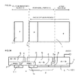
- FIG. 1A is a plan view illustrating main components of a portion of a plane pattern of a peripheral portion of a p type anode diffusion region in a vertical diode as a semiconductor device according to a first embodiment of the invention
- FIG. 1B is a cross-sectional view illustrating a surface portion taken along line a-a' of FIG. 1A
- FIG. 1C is a cross-sectional view illustrating a surface portion taken along line b-b'.
- FIG. 7 is a plan view illustrating a diode chip according to the first embodiment.
- a peripheral portion 2 which is grown from an outer circumferential end 1b of a p type anode diffusion region 1 has a ladder shape as a plane shape.
- a plurality of p type anode stretch-out portions 70 are formed in parallel to each other by stretching out the p type anode diffusion region 1 in a stripe shape from the outer circumferential end 1b of the p type anode diffusion region 1 toward the outer circumference of the peripheral portion 2.
- n type drift layers 10 are exposed in a stripe shape between the adjacent p type anode stretch-out portions 70.
- the p type anode stretch-out portions 70 and the n type drift layers 10 are alternately repeated in the ring direction along the circumference of an anode electrode 7.
- the p type anode stretch-out portions 70 may be expressed to be formed in a ladder shape.
- a ladder-shaped extension portion 60 where the p type anode stretch-out portions 70 are stretched out from the p type anode diffusion region 1 in a ladder shape is formed in the peripheral portion 2.
- the anode electrode 7 configured with an Al-Si alloy is formed on a surface of the p type anode diffusion region 1 to be in ohmic contact with the p type anode diffusion region 1.
- An active region 30 where main current flows is a region where the p type anode diffusion region 1 and the anode electrode 7 are in directly conductive contact with each other.
- the active region 30 is located at a central side (right side of the figure) of an insulating film 3a (for example, a phospho silicate glass: PSG) isolating the anode electrode 7 and a separated electrode described below.
- an insulating film 3a for example, a phospho silicate glass: PSG
- a p type ring-shaped diffusion region 50 (described below) which the outer circumference sides of the p type anode stretch-out portions 70 are in contact with becomes the peripheral portion 2.
- An anode separated electrode 5 (first metal film) having a ring-shaped plane pattern which is in ohmic contact with the p type anode stretch-out portions 70 and surrounds the outer circumference of the anode electrode 7 is formed on a surface of the ladder-shaped extension portion 60 with the insulating film 3a being interposed between the anode separated electrode 5 and the anode electrode 7.
- the anode separated electrode 5 is separated from the anode electrode 7 through the insulating film 3a, so that the anode separated electrode 5 is electrically isolated from the anode electrode 7.
- a p type ring-shaped region 1-1 is installed, and a field plate 6 (second metal film) which is in contact with the p type ring-shaped region 1-1 is formed in a ring-shaped plane pattern surrounding the outer circumference of the p type anode diffusion region 1.
- the p type ring-shaped region 1-1 is installed as a guard ring in the voltage-resistant region 40 outside the outer circumferential end 1a of the p type anode diffusion region 1.
- the p type ring-shaped diffusion region 50 having a diffusion depth larger than that of the p type anode stretch-out portions 70 may be formed so as to be in contact with the p type anode stretch-out portions 70.
- the p type ring-shaped diffusion region 50 may be formed so that a total impurity amount of p type impurities thereof is larger than that of the p type anode diffusion region 1. As a result, the impurity concentration thereof is higher than that of the p type anode diffusion region 1.
- the p type ring-shaped diffusion region 50 is formed so that the radius of curvature of the outer circumferential end 1a thereof is larger than that of the p type anode diffusion region 1. Therefore, it is possible to obtain an effect of alleviating the electric field concentration at a depletion layer expanding when a reverse bias is applied.
- FIG. 1C is a cross-sectional view taken along line b-b' of FIG. 1A and illustrates a surface portion of a substrate where the n type drift layer 10 is exposed.
- the peripheral portion 2 is configured as the ladder-shaped extension portion 60 in order to increase the sheet resistance.
- the ladder-shaped extension portion 60 Due to the ladder-shaped extension portion 60, it is possible to increase the sheet resistance without an increase in a width (distance between the inner circumferential end and the outer circumferential end) of the peripheral portion 2, namely, without an increase in an area of chip in comparison with a diode of the related art.
- the resistance (sheet resistance) of the horizontal direction of the peripheral portion 2 is considered to be higher due to the structure of the p type anode stretch-out portions 70, the current concentration in the vicinity of the outer circumferential end 8 is alleviated.
- the current concentration in the vicinity of the outer circumferential end 8 is alleviated.
- holes are not injected in the exposed portion of the n type drift layer 10 within the p type anode stretch-out portion 70 during the reverse recovery period, remaining carriers are decreased, so that the current concentration is alleviated during the reverse recovery period.
- a ratio of a width (width in the ring direction) of the stripe-shaped p type anode stretch-out portion 70 to a repetition pitch of the stripe-shaped p type anode stretch-out portions 70 and the exposed portions (stripe-shaped substrate surface) of the n type drift layers 10 may be set to be 10% or more and 50% or less. In the case where the ratio is larger than 50%, the sheet resistance is decreased, so that the effect of suppressing injection of minority carriers is decreased. In the case where the ratio is smaller than 10%, the width of the stripe-shaped p type anode stretch-out portions 70 is too small, so that carriers are concentrated on the outer circumferential end 1a.
- the portion which the electric field is concentrated on during the reverse recovery period is a curvature portion of the outer circumferential end 1a.
- the electric field intensity is increased at this portion due to the concentration of current, so the reverse-recovery destruction easily occurs. Therefore, it is preferable that the ratio of the widths of the stripe-shaped p type anode stretch-out portions 70 is 10% or more and 50% or less.
- the sheet resistance of the peripheral portion 2 can be easily controlled by configuring the peripheral portion 2 to be the ladder-shaped extension portion 60, for example, the outer-circumferential-direction length of the ladder-shaped extension portion 60 (length of the stripe-shaped p type anode stretch-out portions 70) may be configured to be short. However, the outer-circumferential-direction length of the ladder-shaped extension portion 60 needs to be secured so as not to increase the injection of holes.
- the p type ring-shaped diffusion region 50 located at the outer circumference side of the peripheral portion 2 is formed to have a higher concentration and a larger diffusion depth than the p type anode diffusion region 1.
- the outer-circumferential-direction length of the ladder-shaped extension portion 60 becomes smaller than the length of the p type ring-shaped diffusion region 50, the injection of minority carriers injected from the p type ring-shaped diffusion region 50 is increased. Accordingly, it is preferable that the outer-circumferential-direction length of the ladder-shaped extension portion 60 is at least equal to or larger than the length of the p type ring-shaped diffusion region 50.
- a width L of the exposed portion (stripe-shaped substrate surface) of the n type drift layer 10 in the ladder-shaped extension portion 60 in the direction (namely, in the ring direction where the ladder structures are repeated) perpendicular to the outer circumferential direction may be configured as follows. First, when the stripe-shaped p type anode stretch-out portions 70 of the ladder-shaped extension portion 60 and the p type anode diffusion region 1 are simultaneously formed, a minimum stripe width and a pitch width caused from a horizontal diffusion region diffused in the surface direction according to the depth of the p type anode diffusion region 1 need to be considered.
- the horizontal diffusion width is set to be 80% of the diffusion depth
- the minimum width of the stripe-shaped p type anode stretch-out portion 70 is equal to or larger than the 160% of the diffusion depth. Therefore, the width of the exposed portion (stripe-shaped substrate surface) of the n type drift layer 10 needs to be set so that the stripe-shaped p type anode stretch-out portions 70 of the two sides facing each other with the stripe-shaped substrate surface interposed therebetween do not overlap each other due to the horizontal diffusion.
- the width L of the exposed portion (stripe-shaped substrate surface) of the n type drift layer 10 is larger than 1.6 times Xj.
- the width of the exposed portion (stripe-shaped substrate surface) of the n type drift layer 10 inserted into the ladder-shaped extension portion 60 is equal to or larger than the diffusion length of the hole carriers.
- the p type anode diffusion region 1 may be extended in the outer circumferential direction, or the ladder-shaped extension portion 60 may be formed so as to be connected to the p type anode diffusion region 1 by using the p type ring-shaped diffusion region 50.
- the sheet resistance of the p type anode diffusion region 1 is, for example, about 1000 ⁇ / ⁇
- the sheet resistance of the p type ring-shaped diffusion region 50 is, for example, 50 ⁇ / ⁇ .
- the sheet resistance of the ladder-shaped extension portion 60 is typically 100 ⁇ / ⁇ .
- the sheet resistance of the ladder-shaped extension portion 60 is 50 ⁇ / ⁇ or more and 300 ⁇ / ⁇ or less.
- the sheet resistance of the ladder-shaped extension portion 60 is 50 ⁇ / ⁇ or more.
- the ratio of the widths of the p type anode stretch-out portions 70 is smaller than 10%, the sheet resistance is substantially 300 ⁇ / ⁇ or more.
- the voltage drop of the holes passing through the ladder-shaped extension portion 60 during the reverse recovery period is increased (for example, 100 V or more). Therefore, most of the hole current flows in the anode separated electrode. At this time, the current is concentrated on the end portion where the anode separated electrode and the ladder-shaped extension portion 60 are in contact with each other, so that the reverse recovery resistant amount is decreased.
- the sheet resistance of the ladder-shaped extension portion 60 is 300 ⁇ / ⁇ or less.
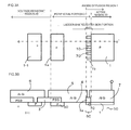
- FIG. 3 is a cross-sectional view illustrating a surface portion of a diode as a semiconductor device according to a second embodiment of the invention.
- the peripheral portion 2 of the p type anode diffusion region 1 includes a ladder-shaped extension portion 60 having a short extension width which is substantially equal to the width of the insulating film 3a for insulating the anode electrode 7 and the anode separated electrode 5 (first metal film).
- the ladder-shaped extension portion 60 is separated from the p type ring-shaped diffusion region 50 which is connected to the anode separated electrode 5.
- the ladder-shaped extension portion 60 and the p type ring-shaped diffusion region 50 are connected to each other through the anode separated electrode 5.
- an increase in area of the ladder-shaped extension portion 60 is suppressed, so that it is possible to increase the sheet resistance.
- the short extension length of the ladder-shaped extension portion 60 which is substantially equal to the width of the insulating film 3a may be equal or larger than the diffusion length of holes. As a result, it is possible to suppress the current density of the current flowing in the ladder-shaped extension portion 60 during the reverse recovery period.
- the exposed portion of the n type drift layer 10 in the peripheral portion 2 since holes are not injected during the reverse recovery period, remaining carriers are decreased, so that the current concentration is alleviated during the reverse recovery period.
- the width of the exposed portion (stripe-shaped substrate surface) of the n type drift layer 10 interposed between the stripe-shaped p type anode stretch-out portions 70 may be equal to that of the first embodiment.
- FIG. 4A is a plan view illustrating a portion of a diode as a semiconductor device according to a third embodiment of the invention
- FIG. 4B is a cross-sectional view taken along line d-d' of FIG. 4A
- the peripheral portion 2 includes the p type ring-shaped diffusion region 50, the stripe-shaped p type anode stretch-out portions 70, and an opening portion 4 which is formed in the insulating film 3, and there is no surface metal film (first metal film 5) which is in ohmic contact illustrated in FIGS. 1A to 1C .
- the ladder-shaped extension portion 60 similarly to the first embodiment, in the ladder-shaped extension portion 60, an increase in area of the p type anode diffusion region 1 is suppressed, so that it is possible to increase the sheet resistance. As a result, it is possible to suppress the current density of the current flowing in the ladder-shaped extension portion 60 during the reverse recovery period.
- the exposed portion of the n type drift layer 10 in the ladder-shaped extension portion 60 since holes are not injected during the reverse recovery period, remaining carriers are decreased, so that the current concentration is alleviated during the reverse recovery period.
- the width of the exposed portion (stripe-shaped substrate surface) of the n type drift layer 10 in the ladder-shaped extension portion 60 may be set to be the same length as that of the first embodiment.
- a passivation film such as a polyimide film or a silicon nitride film is formed on a surface ranging from the voltage-resistant region 40 to a portion of the outer circumference side of the active region 30.
- a passivation film such as a polyimide film or a silicon nitride film is formed on a surface ranging from the voltage-resistant region 40 to a portion of the outer circumference side of the active region 30.
- the surface of the wide opening portion 4 of the peripheral portion 2 is covered with a passivation film.
- FIG. 5 is a cross-sectional view illustrating a surface portion of a diode as a semiconductor device according to a fourth embodiment of the invention.
- the surfaces of the ladder-shaped extension portion 60 and the p type ring-shaped diffusion region 50 of the peripheral portion 2 are covered with an insulating film 3a, and there is no surface metal film (first metal film 5).
- first metal film 5 the surface metal film 5
- the ladder-shaped extension portion 60 similarly to the first embodiment, in the ladder-shaped extension portion 60, an increase in area of the p type anode diffusion region is suppressed, so that it is possible to increase the sheet resistance. As a result, it is possible to suppress the current density of the current flowing in the ladder-shaped extension portion 60 during the reverse recovery period.
- the width of the exposed portion (stripe-shaped substrate surface) of the n type drift layer 10 may be set to be the same length as that of the first embodiment.
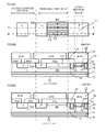
- FIG. 6A is a plan view illustrating main components in a portion of a plane pattern of a peripheral portion in a p type base region of a vertical IGBT as a semiconductor device according to a fifth embodiment of the invention
- FIG. 6B is a cross-sectional view illustrating a surface portion taken along line f-f' of FIG. 6A
- FIG. 6C is a cross-sectional view illustrating a surface portion taken along line g-g' of FIG. 6A .
- a p type base region 11 is installed at a first main surface side (front surface side) of an n- type semiconductor substrate (n type drift layer 10).
- An n type emitter region 12 and a p + contact region 13 which is adjacent to the n type emitter region 12 at the surface thereof are included in a surface layer of the p type base region 11. Furthermore, an active region 30 where a plurality of trenches 20 are arranged to be parallel to each other in a stripe-shaped plane pattern and the p type base region 11 are arranged on the first main surface between the parallel-arranged trenches 20 is included in the first main surface.
- a gate electrode 15 which is configured with a conductive polysilicon is installed within the trench 20 through a gate oxide film 14.
- An emitter electrode 16 is configured to be conductively connected to the surface of the n type emitter region 12 and the surface of the p + contact region 13 to cover the gate electrode through an interlayer insulating film 21. Furthermore, a p type collector layer 17 is installed at a second surface side (rear surface side), and a collector electrode 18 is installed to be in contact with the p type collector layer 17.
- the peripheral portion 19 of the p type base region 11 includes a ladder-shaped extension portion 60 which is configured in a ladder shape.
- a plurality of p type base stretch-out portions 71 are formed by stretching out the p type base region 11 in a stripe shape from the outer circumferential end of the p type base region 11 to the outer circumferential end of peripheral portion 19.
- n type drift layers 10 are exposed in a stripe shape between the adjacent p type base stretch-out portions 71, so that a stripe-shaped substrate surface is formed.
- the p type base stretch-out portions 71 and the stripe-shaped n type drift layers 10 are alternately repeated in the ring direction along the circumference of the emitter electrode 16.
- the p type base stretch-out portions 71 may be expressed to be formed in a ladder shape.
- the ladder-shaped extension portion 60 where the p type base stretch-out portions 71 are stretched out from the p type base region 11 in a ladder shape is formed in the peripheral portion 19. Due to the functions described above in the first to fourth embodiments, the ladder-shaped extension portion 60 becomes a region having high sheet resistance, so that the current concentration in the vicinity of the outer circumferential end of the p type base region 11 is alleviated during the turn-off period.
- An n-channel type MOSFET (not illustrated) is obtained by replacing the p type collector layer 17 of the semiconductor device according to the fifth embodiment of the invention with an n type drain layer of which concentration is higher than that of the n type drift layer 10.
- a parasitic diode (sometimes, referred to as an embedded diode) including a p type base region 11, an n type drift layer 10, and an n type drain layer exists in the MOSFET.
- the ladder-shaped extension portion 60 becomes a region having high sheet resistance due to the functions of the first to fourth embodiments, so that the current concentration in the vicinity of the outer circumferential end of the p type base region 11 is alleviated during the reverse recovery period.
- FIG. 10 illustrates a diode as a semiconductor device according to a seventh embodiment of the invention.
- the seventh embodiment is different from the first embodiment in that the p type ring-shaped diffusion region 50 of the first embodiment is removed.
- the p type anode diffusion region 1 has a large diffusion depth of 5 ⁇ m or more and 30 ⁇ m or less, since the radius of curvature of the end portion of the p type anode diffusion region 1 is sufficiently large, although the p type ring-shaped diffusion region 50 is not formed, the electric field intensity at the end portion of the p type anode diffusion region 1 can be sufficiently alleviated.
- the ladder-shaped extension portion 60 becomes a region having high sheet resistance due to the same function as that of the diode of the first embodiment, so that the current concentration in the vicinity of the outer circumferential end of the p type base region 11 is alleviated during the reverse recovery.
- FIG. 11 is a cross-sectional view illustrating a surface portion of a diode as a semiconductor device according to an eighth embodiment of the invention.
- the eighth embodiment is different from the fourth embodiment in that the p type ring-shaped diffusion region 50 of the fourth embodiment is removed.
- the p type anode diffusion region 1 has a large diffusion depth of 5 ⁇ m or more and 30 ⁇ m or less, since the radius of curvature of the end portion of the p type anode diffusion region 1 is sufficiently large, although the p type ring-shaped diffusion region 50 is not formed, the electric field intensity at the end portion of the p type anode diffusion region 1 can be sufficiently alleviated.
- the ladder-shaped extension portion 60 becomes a region having high sheet resistance due to the same function as that of the diode of the first embodiment, so that the current concentration in the vicinity of the outer circumferential end of the p type base region 11 is alleviated during the reverse recovery period.
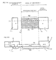
- FIG. 12 is a cross-sectional view illustrating a surface portion of a diode as a semiconductor device according to a ninth embodiment of the invention.
- FIG. 13 is a plan view illustrating overall portions of the diode as the semiconductor device according to the ninth embodiment of the invention including FIG. 12.
- FIG. 12A is an enlarged plan view illustrating a portion indicated by a broken line area in FIG. 13 ;
- FIG. 12B is a cross-sectional view taken along line k-k' of FIG. 12A;
- FIG. 12C is a cross-sectional view taken along line l-l' of FIG. 12A .
- a peripheral portion 2 includes a lattice-shaped stretch-out portion 60a which is patterned in a lattice shape instead of the ladder-shaped extension portion 60 of the first embodiment.
- all the surfaces of the lattice-shaped stretch-out portion 60a and the p type ring-shaped diffusion region 50 are covered with an insulating film 3a, and the insulating film 3 is covered with an anode electrode extension portion 5a of an anode electrode 7 extended to the peripheral portion 2.
- the lattice-shaped stretch-out portion 60a is different from the ladder-shaped extension portions 60 according to the first to eighth embodiments in terms of a plane pattern.
- the ninth embodiment is different from the first to eight embodiments in that the edge shape (plane shape of the end portion) of the side of the active region 30 of the insulating film 3 covering the upper portion of the peripheral portion 2 is a curve shape instead of a straight line shape. The two different points will be described below.
- the edge shape plane shape of the end portion of the side of the active region 30 of the insulating film 3 covering the upper portion of the peripheral portion 2 is a curve shape instead of a straight line shape.
- the pattern of the lattice-shaped stretch-out portion 60a which becomes a path of current during the reverse recovery period, has an inclined lattice shape instead of a ladder shape of the ladder-shaped extension portion 60.
- the p type lattice line portion 51 is formed to be inclined instead of being perpendicular to the direction toward the outer circumference, the distance in the direction toward the outer circumference can be increased in comparison with the above-described stripe shaped pattern. Therefore, it is possible to easily increase the sheet resistance. Accordingly, the effect of suppressing current concentration during the reverse recovery is improved.
- the rated voltage is in a range of 600 V to 6500 V, for example, 1200 V.
- the resistivity of a semiconductor substrate (for example, silicon) constituting the n- drift layer corresponding to the rated voltage is in a range of 20 ⁇ cm to 500 ⁇ cm, for example, 50 ⁇ cm.
- the thickness of the substrate is in a range of 60 ⁇ m to 500 ⁇ m, for example, 120 ⁇ m.
- the surface concentration of the p type anode diffusion region is in a range of 1 ⁇ 10 16 /cm 3 to 1 ⁇ 10 18 /cm 3 , for example, 3 ⁇ 10 16 /cm 3 .
- the diffusion depth of the layer is in a range of 1 ⁇ m to 5 ⁇ m, for example, 3 ⁇ m.
- the width of the peripheral portion 2 is 100 (m or more and 1000 (m or less, for example, 300 (m.
- the same specifications described hereinbefore are applied to the first to eighth embodiments as well as the ninth embodiment.
- the width of the p type lattice line portions 51 constituting the lattice pattern of the lattice-shaped stretch-out portion 60a is, for example, 3 (m or more 100 (m or less.
- p type impurity (boron or the like) ions are injected. If the width of opening of a mask used for the ion injection is set to 1 (m, the width of the p type lattice line portion 51 becomes 3 (m including the horizontal diffusion portion (about 80% of the vertical directional portion) when the diffusion depth is 2 (m. If the width of the p type lattice line portion 51 is set to 3 (m, the sheet resistance of the lattice-shaped stretch-out portion 60a can be configured to be 300 (/( or less.
- the length of the resistant voltage structure region is typical in a range of 100 ⁇ m (for example, in the case of the rated voltage of 600 V) to 700 ⁇ m (for example, in the case of the rated voltage of 3.3 kV). Therefore, in the case of the rated voltage of about 600 V, the region having the width of the p type lattice line portion 51 becomes the resistant voltage structure region.
- the width of the p type lattice line portion 51 is set to 100 ⁇ m
- the lattice-shaped pattern is formed by using the p type lattice line portions 51, and the length of the lattice-shaped stretch-out portion 60a is larger than 100 ⁇ m. Therefore, it is preferable that the width of the p type lattice line portion 51 is 100 ⁇ m or less.
- the repetition pitch W of the p type lattice line portions 51 adjacent to each other in parallel among the p type lattice line portions 51 in the lattice-shaped pattern is 4 ⁇ m or more and 200 ⁇ m or less.
- the pitch is 4 ⁇ m or more.
- the ratio of the width of the p type lattice line portion 51 to the pitch W is preferably 50% or less as described above, it is preferable that the pitch W is 6 ⁇ m or more.
- the pitch W is 500 ⁇ m or less.
- FIG. 14 is an enlarged plan view illustrating a vicinity of an interlayer insulating film end portion 22 corresponding to the boundary between the active region 30 and the peripheral portion 2 according to the ninth embodiment illustrated in FIGS. 12A to 12C .
- the interlayer insulating film end portion 22 is configured to be separated by the longest distance d from the site where the maximum amount of the hole current 52 is collected during the reverse recovery period. Therefore, the position of the highest hole current density can be configured to separated by a long distance from the interlayer insulating film end portion 22. As illustrated in FIG.
- the relation between the distance d and the above-described pitch W is d ⁇ Wsin ⁇ if the angle between the p type lattice line portion 51 and the direction perpendicular to the outer circumferential direction of the chip is defined by ⁇ .
- the edge (end portion) shape of the insulating film 3 covering the lattice-shaped extension portion 60a at the side of the active region 30 is configured in accordance with the flow distribution of the reverse recovery current caused by the inclined lattice-shaped pattern.
- the overhang length of the insulating film 3 at the site where the hole current is collected during the reverse recovery period is configured to be large, and the overhang length of the insulating film 3 at the site where the hole current is distributed so as to be small is configured to be small.
- the end portion of the insulating film 3 is configured to be a curve shape according the above-described determination condition, so that it is possible to alleviate the current concentration at the end portion of the insulating film 3.
- the width of the peripheral portion 2 can be reduced by at least 10% without a decrease in the reverse recovery resistant amount in comparison with the case of the related art.
- the chip size can be reduced, the yield of chips per wafer is also increased, and the unit price of chip can be reduced.
Landscapes
- Electrodes Of Semiconductors (AREA)
- Metal-Oxide And Bipolar Metal-Oxide Semiconductor Integrated Circuits (AREA)
- Thyristors (AREA)
- Chemical & Material Sciences (AREA)
- Composite Materials (AREA)
Applications Claiming Priority (2)
| Application Number | Priority Date | Filing Date | Title |
|---|---|---|---|
| JP2012115494 | 2012-05-21 | ||
| JP2013006206A JP6107156B2 (ja) | 2012-05-21 | 2013-01-17 | 半導体装置 |
Publications (3)
| Publication Number | Publication Date |
|---|---|
| EP2667418A2 true EP2667418A2 (de) | 2013-11-27 |
| EP2667418A3 EP2667418A3 (de) | 2014-02-12 |
| EP2667418B1 EP2667418B1 (de) | 2019-08-21 |
Family
ID=48463811
Family Applications (1)
| Application Number | Title | Priority Date | Filing Date |
|---|---|---|---|
| EP13168372.4A Active EP2667418B1 (de) | 2012-05-21 | 2013-05-17 | Halbleiterbauelement |
Country Status (4)
| Country | Link |
|---|---|
| US (1) | US9236460B2 (de) |
| EP (1) | EP2667418B1 (de) |
| JP (1) | JP6107156B2 (de) |
| CN (1) | CN103426911B (de) |
Families Citing this family (11)
| Publication number | Priority date | Publication date | Assignee | Title |
|---|---|---|---|---|
| US9614043B2 (en) | 2012-02-09 | 2017-04-04 | Vishay-Siliconix | MOSFET termination trench |
| US9842911B2 (en) | 2012-05-30 | 2017-12-12 | Vishay-Siliconix | Adaptive charge balanced edge termination |
| EP2942816B1 (de) * | 2013-08-15 | 2020-10-28 | Fuji Electric Co., Ltd. | Halbleiterbauelement |
| US9887259B2 (en) | 2014-06-23 | 2018-02-06 | Vishay-Siliconix | Modulated super junction power MOSFET devices |
| JP6413467B2 (ja) * | 2014-08-19 | 2018-10-31 | 富士電機株式会社 | 半導体装置 |
| KR102098996B1 (ko) | 2014-08-19 | 2020-04-08 | 비쉐이-실리코닉스 | 초접합 금속 산화물 반도체 전계 효과 트랜지스터 |
| WO2016114138A1 (ja) | 2015-01-14 | 2016-07-21 | 富士電機株式会社 | 半導体装置 |
| JP6550995B2 (ja) | 2015-07-16 | 2019-07-31 | 富士電機株式会社 | 半導体装置 |
| CN111063723B (zh) * | 2019-11-25 | 2021-12-28 | 深圳深爱半导体股份有限公司 | 开关集成控制器 |
| JPWO2024203119A1 (de) * | 2023-03-30 | 2024-10-03 | ||
| WO2024203121A1 (ja) * | 2023-03-30 | 2024-10-03 | ローム株式会社 | 半導体装置 |
Citations (5)
| Publication number | Priority date | Publication date | Assignee | Title |
|---|---|---|---|---|
| JPH09232597A (ja) | 1996-02-28 | 1997-09-05 | Hitachi Ltd | ダイオード及び電力変換装置 |
| JP2010050441A (ja) | 2008-07-22 | 2010-03-04 | Fuji Electric Systems Co Ltd | 半導体装置 |
| JP2011049399A (ja) | 2009-08-27 | 2011-03-10 | Toyota Motor Corp | 半導体装置 |
| JP2011171401A (ja) | 2010-02-17 | 2011-09-01 | Sansha Electric Mfg Co Ltd | Pinダイオード |
| JP2011171363A (ja) | 2010-02-16 | 2011-09-01 | Sansha Electric Mfg Co Ltd | Pinダイオード |
Family Cites Families (16)
| Publication number | Priority date | Publication date | Assignee | Title |
|---|---|---|---|---|
| JP2000114550A (ja) * | 1998-10-06 | 2000-04-21 | Hitachi Ltd | ダイオード及び電力変換装置 |
| US6603185B1 (en) * | 1999-02-01 | 2003-08-05 | Fuji Electric Co., Ltd. | Voltage withstanding structure for a semiconductor device |
| JP3778061B2 (ja) * | 2001-11-19 | 2006-05-24 | 富士電機デバイステクノロジー株式会社 | 高耐圧icの製造方法 |
| JP3908572B2 (ja) * | 2002-03-18 | 2007-04-25 | 株式会社東芝 | 半導体素子 |
| JP4469584B2 (ja) * | 2003-09-12 | 2010-05-26 | 株式会社東芝 | 半導体装置 |
| JP4904673B2 (ja) * | 2004-02-09 | 2012-03-28 | 富士電機株式会社 | 半導体装置および半導体装置の製造方法 |
| JP2006005275A (ja) * | 2004-06-21 | 2006-01-05 | Toshiba Corp | 電力用半導体素子 |
| JP4967236B2 (ja) * | 2004-08-04 | 2012-07-04 | 富士電機株式会社 | 半導体素子 |
| JP5196766B2 (ja) * | 2006-11-20 | 2013-05-15 | 株式会社東芝 | 半導体装置 |
| US8008734B2 (en) * | 2007-01-11 | 2011-08-30 | Fuji Electric Co., Ltd. | Power semiconductor device |
| JP4635067B2 (ja) * | 2008-03-24 | 2011-02-16 | 株式会社東芝 | 半導体装置及びその製造方法 |
| US8174067B2 (en) * | 2008-12-08 | 2012-05-08 | Fairchild Semiconductor Corporation | Trench-based power semiconductor devices with increased breakdown voltage characteristics |
| WO2011013379A1 (en) * | 2009-07-31 | 2011-02-03 | Fuji Electric Systems Co., Ltd. | Semiconductor apparatus |
| FR2958452B1 (fr) | 2010-03-30 | 2012-06-15 | Alstom Transport Sa | Anneaux d'extension de terminaison de jonction |
| JP5671867B2 (ja) * | 2010-08-04 | 2015-02-18 | 富士電機株式会社 | 半導体装置およびその製造方法 |
| JP2012199434A (ja) * | 2011-03-22 | 2012-10-18 | Toshiba Corp | 半導体装置 |
-
2013
- 2013-01-17 JP JP2013006206A patent/JP6107156B2/ja active Active
- 2013-05-10 CN CN201310173163.5A patent/CN103426911B/zh active Active
- 2013-05-16 US US13/896,305 patent/US9236460B2/en active Active
- 2013-05-17 EP EP13168372.4A patent/EP2667418B1/de active Active
Patent Citations (5)
| Publication number | Priority date | Publication date | Assignee | Title |
|---|---|---|---|---|
| JPH09232597A (ja) | 1996-02-28 | 1997-09-05 | Hitachi Ltd | ダイオード及び電力変換装置 |
| JP2010050441A (ja) | 2008-07-22 | 2010-03-04 | Fuji Electric Systems Co Ltd | 半導体装置 |
| JP2011049399A (ja) | 2009-08-27 | 2011-03-10 | Toyota Motor Corp | 半導体装置 |
| JP2011171363A (ja) | 2010-02-16 | 2011-09-01 | Sansha Electric Mfg Co Ltd | Pinダイオード |
| JP2011171401A (ja) | 2010-02-17 | 2011-09-01 | Sansha Electric Mfg Co Ltd | Pinダイオード |
Also Published As
| Publication number | Publication date |
|---|---|
| EP2667418B1 (de) | 2019-08-21 |
| CN103426911A (zh) | 2013-12-04 |
| JP6107156B2 (ja) | 2017-04-05 |
| US20130307019A1 (en) | 2013-11-21 |
| EP2667418A3 (de) | 2014-02-12 |
| US9236460B2 (en) | 2016-01-12 |
| CN103426911B (zh) | 2016-08-10 |
| JP2014003271A (ja) | 2014-01-09 |
Similar Documents
| Publication | Publication Date | Title |
|---|---|---|
| US9236460B2 (en) | Semiconductor device having a diffusion region | |
| JP7230969B2 (ja) | 半導体装置 | |
| US9673309B2 (en) | Semiconductor device and method for fabricating semiconductor device | |
| JP5366297B2 (ja) | 半導体装置 | |
| EP2725623B1 (de) | Halbleiterbauelement | |
| JP7030515B2 (ja) | 逆導通半導体装置 | |
| EP2822038B1 (de) | Bipolarer transistor mit isoliertem gate | |
| CN109755293B (zh) | 半导体装置 | |
| US10692999B2 (en) | High voltage MOSFET devices and methods of making the devices | |
| CN111164762B (zh) | 肖特基二极管与mosfet的集成 | |
| EP2517249B1 (de) | Leistungsthyristor mit integriertem Abschaltgate | |
| JP7404722B2 (ja) | 半導体装置 | |
| CN114284336B (zh) | 半导体装置 | |
| JP6597102B2 (ja) | 半導体装置 | |
| JP7533146B2 (ja) | 半導体装置 | |
| EP3154091A1 (de) | Rückwärtsleitendes halbleiterbauelement | |
| US10056501B2 (en) | Power diode with improved reverse-recovery immunity | |
| CN107833915B (zh) | 半导体器件 | |
| US20160240640A1 (en) | Power semiconductor device | |
| JPH06283727A (ja) | 電力用半導体素子 | |
| US9147757B2 (en) | Power semiconductor device and method for manufacturing the same | |
| US20250159926A1 (en) | Semiconductor device | |
| US20260059778A1 (en) | Semiconductor device | |
| JP2004221456A (ja) | 半導体装置 |
Legal Events
| Date | Code | Title | Description |
|---|---|---|---|
| PUAI | Public reference made under article 153(3) epc to a published international application that has entered the european phase |
Free format text: ORIGINAL CODE: 0009012 |
|
| AK | Designated contracting states |
Kind code of ref document: A2 Designated state(s): AL AT BE BG CH CY CZ DE DK EE ES FI FR GB GR HR HU IE IS IT LI LT LU LV MC MK MT NL NO PL PT RO RS SE SI SK SM TR |
|
| AX | Request for extension of the european patent |
Extension state: BA ME |
|
| PUAL | Search report despatched |
Free format text: ORIGINAL CODE: 0009013 |
|
| RIN1 | Information on inventor provided before grant (corrected) |
Inventor name: MATSUI, TOSHIYUKI Inventor name: MOMOTA, SEIJI Inventor name: SHIIGI, TAKASHI Inventor name: KOYAMA, HIROMI Inventor name: FUKUCHI AKIHIRO |
|
| AK | Designated contracting states |
Kind code of ref document: A3 Designated state(s): AL AT BE BG CH CY CZ DE DK EE ES FI FR GB GR HR HU IE IS IT LI LT LU LV MC MK MT NL NO PL PT RO RS SE SI SK SM TR |
|
| AX | Request for extension of the european patent |
Extension state: BA ME |
|
| RIC1 | Information provided on ipc code assigned before grant |
Ipc: H01L 29/739 20060101ALI20140103BHEP Ipc: H01L 29/40 20060101ALN20140103BHEP Ipc: H01L 29/78 20060101AFI20140103BHEP Ipc: H01L 29/06 20060101ALI20140103BHEP Ipc: H01L 29/861 20060101ALI20140103BHEP |
|
| 17P | Request for examination filed |
Effective date: 20140812 |
|
| RBV | Designated contracting states (corrected) |
Designated state(s): AL AT BE BG CH CY CZ DE DK EE ES FI FR GB GR HR HU IE IS IT LI LT LU LV MC MK MT NL NO PL PT RO RS SE SI SK SM TR |
|
| 17Q | First examination report despatched |
Effective date: 20151028 |
|
| GRAP | Despatch of communication of intention to grant a patent |
Free format text: ORIGINAL CODE: EPIDOSNIGR1 |
|
| STAA | Information on the status of an ep patent application or granted ep patent |
Free format text: STATUS: GRANT OF PATENT IS INTENDED |
|
| RIC1 | Information provided on ipc code assigned before grant |
Ipc: H01L 29/861 20060101ALI20190206BHEP Ipc: H01L 29/06 20060101ALI20190206BHEP Ipc: H01L 29/78 20060101AFI20190206BHEP Ipc: H01L 29/40 20060101ALN20190206BHEP Ipc: H01L 29/739 20060101ALI20190206BHEP |
|
| RIC1 | Information provided on ipc code assigned before grant |
Ipc: H01L 29/861 20060101ALI20190221BHEP Ipc: H01L 29/06 20060101ALI20190221BHEP Ipc: H01L 29/40 20060101ALN20190221BHEP Ipc: H01L 29/78 20060101AFI20190221BHEP Ipc: H01L 29/739 20060101ALI20190221BHEP |
|
| INTG | Intention to grant announced |
Effective date: 20190312 |
|
| RIN1 | Information on inventor provided before grant (corrected) |
Inventor name: KOYAMA, HIROMI Inventor name: MOMOTA, SEIJI Inventor name: MATSUI, TOSHIYUKI Inventor name: FUKUCHI AKIHIRO Inventor name: SHIIGI, TAKASHI |
|
| GRAS | Grant fee paid |
Free format text: ORIGINAL CODE: EPIDOSNIGR3 |
|
| GRAA | (expected) grant |
Free format text: ORIGINAL CODE: 0009210 |
|
| STAA | Information on the status of an ep patent application or granted ep patent |
Free format text: STATUS: THE PATENT HAS BEEN GRANTED |
|
| AK | Designated contracting states |
Kind code of ref document: B1 Designated state(s): AL AT BE BG CH CY CZ DE DK EE ES FI FR GB GR HR HU IE IS IT LI LT LU LV MC MK MT NL NO PL PT RO RS SE SI SK SM TR |
|
| REG | Reference to a national code |
Ref country code: GB Ref legal event code: FG4D |
|
| REG | Reference to a national code |
Ref country code: CH Ref legal event code: EP |
|
| REG | Reference to a national code |
Ref country code: DE Ref legal event code: R096 Ref document number: 602013059375 Country of ref document: DE |
|
| REG | Reference to a national code |
Ref country code: AT Ref legal event code: REF Ref document number: 1170734 Country of ref document: AT Kind code of ref document: T Effective date: 20190915 |
|
| REG | Reference to a national code |
Ref country code: IE Ref legal event code: FG4D |
|
| REG | Reference to a national code |
Ref country code: LT Ref legal event code: MG4D |
|
| REG | Reference to a national code |
Ref country code: NL Ref legal event code: MP Effective date: 20190821 |
|
| PG25 | Lapsed in a contracting state [announced via postgrant information from national office to epo] |
Ref country code: FI Free format text: LAPSE BECAUSE OF FAILURE TO SUBMIT A TRANSLATION OF THE DESCRIPTION OR TO PAY THE FEE WITHIN THE PRESCRIBED TIME-LIMIT Effective date: 20190821 Ref country code: NO Free format text: LAPSE BECAUSE OF FAILURE TO SUBMIT A TRANSLATION OF THE DESCRIPTION OR TO PAY THE FEE WITHIN THE PRESCRIBED TIME-LIMIT Effective date: 20191121 Ref country code: NL Free format text: LAPSE BECAUSE OF FAILURE TO SUBMIT A TRANSLATION OF THE DESCRIPTION OR TO PAY THE FEE WITHIN THE PRESCRIBED TIME-LIMIT Effective date: 20190821 Ref country code: BG Free format text: LAPSE BECAUSE OF FAILURE TO SUBMIT A TRANSLATION OF THE DESCRIPTION OR TO PAY THE FEE WITHIN THE PRESCRIBED TIME-LIMIT Effective date: 20191121 Ref country code: SE Free format text: LAPSE BECAUSE OF FAILURE TO SUBMIT A TRANSLATION OF THE DESCRIPTION OR TO PAY THE FEE WITHIN THE PRESCRIBED TIME-LIMIT Effective date: 20190821 Ref country code: HR Free format text: LAPSE BECAUSE OF FAILURE TO SUBMIT A TRANSLATION OF THE DESCRIPTION OR TO PAY THE FEE WITHIN THE PRESCRIBED TIME-LIMIT Effective date: 20190821 Ref country code: LT Free format text: LAPSE BECAUSE OF FAILURE TO SUBMIT A TRANSLATION OF THE DESCRIPTION OR TO PAY THE FEE WITHIN THE PRESCRIBED TIME-LIMIT Effective date: 20190821 Ref country code: PT Free format text: LAPSE BECAUSE OF FAILURE TO SUBMIT A TRANSLATION OF THE DESCRIPTION OR TO PAY THE FEE WITHIN THE PRESCRIBED TIME-LIMIT Effective date: 20191223 |
|
| PG25 | Lapsed in a contracting state [announced via postgrant information from national office to epo] |
Ref country code: IS Free format text: LAPSE BECAUSE OF FAILURE TO SUBMIT A TRANSLATION OF THE DESCRIPTION OR TO PAY THE FEE WITHIN THE PRESCRIBED TIME-LIMIT Effective date: 20191221 Ref country code: RS Free format text: LAPSE BECAUSE OF FAILURE TO SUBMIT A TRANSLATION OF THE DESCRIPTION OR TO PAY THE FEE WITHIN THE PRESCRIBED TIME-LIMIT Effective date: 20190821 Ref country code: LV Free format text: LAPSE BECAUSE OF FAILURE TO SUBMIT A TRANSLATION OF THE DESCRIPTION OR TO PAY THE FEE WITHIN THE PRESCRIBED TIME-LIMIT Effective date: 20190821 Ref country code: AL Free format text: LAPSE BECAUSE OF FAILURE TO SUBMIT A TRANSLATION OF THE DESCRIPTION OR TO PAY THE FEE WITHIN THE PRESCRIBED TIME-LIMIT Effective date: 20190821 Ref country code: ES Free format text: LAPSE BECAUSE OF FAILURE TO SUBMIT A TRANSLATION OF THE DESCRIPTION OR TO PAY THE FEE WITHIN THE PRESCRIBED TIME-LIMIT Effective date: 20190821 Ref country code: GR Free format text: LAPSE BECAUSE OF FAILURE TO SUBMIT A TRANSLATION OF THE DESCRIPTION OR TO PAY THE FEE WITHIN THE PRESCRIBED TIME-LIMIT Effective date: 20191122 |
|
| REG | Reference to a national code |
Ref country code: AT Ref legal event code: MK05 Ref document number: 1170734 Country of ref document: AT Kind code of ref document: T Effective date: 20190821 |
|
| PG25 | Lapsed in a contracting state [announced via postgrant information from national office to epo] |
Ref country code: TR Free format text: LAPSE BECAUSE OF FAILURE TO SUBMIT A TRANSLATION OF THE DESCRIPTION OR TO PAY THE FEE WITHIN THE PRESCRIBED TIME-LIMIT Effective date: 20190821 |
|
| PG25 | Lapsed in a contracting state [announced via postgrant information from national office to epo] |
Ref country code: EE Free format text: LAPSE BECAUSE OF FAILURE TO SUBMIT A TRANSLATION OF THE DESCRIPTION OR TO PAY THE FEE WITHIN THE PRESCRIBED TIME-LIMIT Effective date: 20190821 Ref country code: PL Free format text: LAPSE BECAUSE OF FAILURE TO SUBMIT A TRANSLATION OF THE DESCRIPTION OR TO PAY THE FEE WITHIN THE PRESCRIBED TIME-LIMIT Effective date: 20190821 Ref country code: DK Free format text: LAPSE BECAUSE OF FAILURE TO SUBMIT A TRANSLATION OF THE DESCRIPTION OR TO PAY THE FEE WITHIN THE PRESCRIBED TIME-LIMIT Effective date: 20190821 Ref country code: RO Free format text: LAPSE BECAUSE OF FAILURE TO SUBMIT A TRANSLATION OF THE DESCRIPTION OR TO PAY THE FEE WITHIN THE PRESCRIBED TIME-LIMIT Effective date: 20190821 Ref country code: AT Free format text: LAPSE BECAUSE OF FAILURE TO SUBMIT A TRANSLATION OF THE DESCRIPTION OR TO PAY THE FEE WITHIN THE PRESCRIBED TIME-LIMIT Effective date: 20190821 Ref country code: IT Free format text: LAPSE BECAUSE OF FAILURE TO SUBMIT A TRANSLATION OF THE DESCRIPTION OR TO PAY THE FEE WITHIN THE PRESCRIBED TIME-LIMIT Effective date: 20190821 |
|
| PG25 | Lapsed in a contracting state [announced via postgrant information from national office to epo] |
Ref country code: SK Free format text: LAPSE BECAUSE OF FAILURE TO SUBMIT A TRANSLATION OF THE DESCRIPTION OR TO PAY THE FEE WITHIN THE PRESCRIBED TIME-LIMIT Effective date: 20190821 Ref country code: SM Free format text: LAPSE BECAUSE OF FAILURE TO SUBMIT A TRANSLATION OF THE DESCRIPTION OR TO PAY THE FEE WITHIN THE PRESCRIBED TIME-LIMIT Effective date: 20190821 Ref country code: CZ Free format text: LAPSE BECAUSE OF FAILURE TO SUBMIT A TRANSLATION OF THE DESCRIPTION OR TO PAY THE FEE WITHIN THE PRESCRIBED TIME-LIMIT Effective date: 20190821 Ref country code: IS Free format text: LAPSE BECAUSE OF FAILURE TO SUBMIT A TRANSLATION OF THE DESCRIPTION OR TO PAY THE FEE WITHIN THE PRESCRIBED TIME-LIMIT Effective date: 20200224 |
|
| REG | Reference to a national code |
Ref country code: DE Ref legal event code: R097 Ref document number: 602013059375 Country of ref document: DE |
|
| PLBE | No opposition filed within time limit |
Free format text: ORIGINAL CODE: 0009261 |
|
| STAA | Information on the status of an ep patent application or granted ep patent |
Free format text: STATUS: NO OPPOSITION FILED WITHIN TIME LIMIT |
|
| PG2D | Information on lapse in contracting state deleted |
Ref country code: IS |
|
| 26N | No opposition filed |
Effective date: 20200603 |
|
| PG25 | Lapsed in a contracting state [announced via postgrant information from national office to epo] |
Ref country code: SI Free format text: LAPSE BECAUSE OF FAILURE TO SUBMIT A TRANSLATION OF THE DESCRIPTION OR TO PAY THE FEE WITHIN THE PRESCRIBED TIME-LIMIT Effective date: 20190821 |
|
| PG25 | Lapsed in a contracting state [announced via postgrant information from national office to epo] |
Ref country code: MC Free format text: LAPSE BECAUSE OF FAILURE TO SUBMIT A TRANSLATION OF THE DESCRIPTION OR TO PAY THE FEE WITHIN THE PRESCRIBED TIME-LIMIT Effective date: 20190821 Ref country code: LI Free format text: LAPSE BECAUSE OF NON-PAYMENT OF DUE FEES Effective date: 20200531 Ref country code: CH Free format text: LAPSE BECAUSE OF NON-PAYMENT OF DUE FEES Effective date: 20200531 |
|
| REG | Reference to a national code |
Ref country code: BE Ref legal event code: MM Effective date: 20200531 |
|
| GBPC | Gb: european patent ceased through non-payment of renewal fee |
Effective date: 20200517 |
|
| PG25 | Lapsed in a contracting state [announced via postgrant information from national office to epo] |
Ref country code: LU Free format text: LAPSE BECAUSE OF NON-PAYMENT OF DUE FEES Effective date: 20200517 |
|
| PG25 | Lapsed in a contracting state [announced via postgrant information from national office to epo] |
Ref country code: FR Free format text: LAPSE BECAUSE OF NON-PAYMENT OF DUE FEES Effective date: 20200531 Ref country code: GB Free format text: LAPSE BECAUSE OF NON-PAYMENT OF DUE FEES Effective date: 20200517 Ref country code: IE Free format text: LAPSE BECAUSE OF NON-PAYMENT OF DUE FEES Effective date: 20200517 |
|
| PG25 | Lapsed in a contracting state [announced via postgrant information from national office to epo] |
Ref country code: BE Free format text: LAPSE BECAUSE OF NON-PAYMENT OF DUE FEES Effective date: 20200531 |
|
| PG25 | Lapsed in a contracting state [announced via postgrant information from national office to epo] |
Ref country code: MT Free format text: LAPSE BECAUSE OF FAILURE TO SUBMIT A TRANSLATION OF THE DESCRIPTION OR TO PAY THE FEE WITHIN THE PRESCRIBED TIME-LIMIT Effective date: 20190821 Ref country code: CY Free format text: LAPSE BECAUSE OF FAILURE TO SUBMIT A TRANSLATION OF THE DESCRIPTION OR TO PAY THE FEE WITHIN THE PRESCRIBED TIME-LIMIT Effective date: 20190821 |
|
| PG25 | Lapsed in a contracting state [announced via postgrant information from national office to epo] |
Ref country code: MK Free format text: LAPSE BECAUSE OF FAILURE TO SUBMIT A TRANSLATION OF THE DESCRIPTION OR TO PAY THE FEE WITHIN THE PRESCRIBED TIME-LIMIT Effective date: 20190821 |
|
| REG | Reference to a national code |
Ref country code: DE Ref legal event code: R079 Ref document number: 602013059375 Country of ref document: DE Free format text: PREVIOUS MAIN CLASS: H01L0029780000 Ipc: H10D0030600000 |
|
| PGFP | Annual fee paid to national office [announced via postgrant information from national office to epo] |
Ref country code: DE Payment date: 20250402 Year of fee payment: 13 |