EP2565301B1 - Silicon carbide crystal and method for producing silicon carbide crystal - Google Patents
Silicon carbide crystal and method for producing silicon carbide crystal Download PDFInfo
- Publication number
- EP2565301B1 EP2565301B1 EP11774697.4A EP11774697A EP2565301B1 EP 2565301 B1 EP2565301 B1 EP 2565301B1 EP 11774697 A EP11774697 A EP 11774697A EP 2565301 B1 EP2565301 B1 EP 2565301B1
- Authority
- EP
- European Patent Office
- Prior art keywords
- source material
- sic crystal
- silicon carbide
- crystal
- ppm
- Prior art date
- Legal status (The legal status is an assumption and is not a legal conclusion. Google has not performed a legal analysis and makes no representation as to the accuracy of the status listed.)
- Active
Links
Images
Classifications
-
- C—CHEMISTRY; METALLURGY
- C30—CRYSTAL GROWTH
- C30B—SINGLE-CRYSTAL GROWTH; UNIDIRECTIONAL SOLIDIFICATION OF EUTECTIC MATERIAL OR UNIDIRECTIONAL DEMIXING OF EUTECTOID MATERIAL; REFINING BY ZONE-MELTING OF MATERIAL; PRODUCTION OF A HOMOGENEOUS POLYCRYSTALLINE MATERIAL WITH DEFINED STRUCTURE; SINGLE CRYSTALS OR HOMOGENEOUS POLYCRYSTALLINE MATERIAL WITH DEFINED STRUCTURE; AFTER-TREATMENT OF SINGLE CRYSTALS OR A HOMOGENEOUS POLYCRYSTALLINE MATERIAL WITH DEFINED STRUCTURE; APPARATUS THEREFOR
- C30B23/00—Single-crystal growth by condensing evaporated or sublimed materials
- C30B23/02—Epitaxial-layer growth
- C30B23/06—Heating of the deposition chamber, the substrate or the materials to be evaporated
-
- C—CHEMISTRY; METALLURGY
- C30—CRYSTAL GROWTH
- C30B—SINGLE-CRYSTAL GROWTH; UNIDIRECTIONAL SOLIDIFICATION OF EUTECTIC MATERIAL OR UNIDIRECTIONAL DEMIXING OF EUTECTOID MATERIAL; REFINING BY ZONE-MELTING OF MATERIAL; PRODUCTION OF A HOMOGENEOUS POLYCRYSTALLINE MATERIAL WITH DEFINED STRUCTURE; SINGLE CRYSTALS OR HOMOGENEOUS POLYCRYSTALLINE MATERIAL WITH DEFINED STRUCTURE; AFTER-TREATMENT OF SINGLE CRYSTALS OR A HOMOGENEOUS POLYCRYSTALLINE MATERIAL WITH DEFINED STRUCTURE; APPARATUS THEREFOR
- C30B23/00—Single-crystal growth by condensing evaporated or sublimed materials
- C30B23/02—Epitaxial-layer growth
- C30B23/025—Epitaxial-layer growth characterised by the substrate
-
- C—CHEMISTRY; METALLURGY
- C30—CRYSTAL GROWTH
- C30B—SINGLE-CRYSTAL GROWTH; UNIDIRECTIONAL SOLIDIFICATION OF EUTECTIC MATERIAL OR UNIDIRECTIONAL DEMIXING OF EUTECTOID MATERIAL; REFINING BY ZONE-MELTING OF MATERIAL; PRODUCTION OF A HOMOGENEOUS POLYCRYSTALLINE MATERIAL WITH DEFINED STRUCTURE; SINGLE CRYSTALS OR HOMOGENEOUS POLYCRYSTALLINE MATERIAL WITH DEFINED STRUCTURE; AFTER-TREATMENT OF SINGLE CRYSTALS OR A HOMOGENEOUS POLYCRYSTALLINE MATERIAL WITH DEFINED STRUCTURE; APPARATUS THEREFOR
- C30B23/00—Single-crystal growth by condensing evaporated or sublimed materials
- C30B23/02—Epitaxial-layer growth
-
- C—CHEMISTRY; METALLURGY
- C30—CRYSTAL GROWTH
- C30B—SINGLE-CRYSTAL GROWTH; UNIDIRECTIONAL SOLIDIFICATION OF EUTECTIC MATERIAL OR UNIDIRECTIONAL DEMIXING OF EUTECTOID MATERIAL; REFINING BY ZONE-MELTING OF MATERIAL; PRODUCTION OF A HOMOGENEOUS POLYCRYSTALLINE MATERIAL WITH DEFINED STRUCTURE; SINGLE CRYSTALS OR HOMOGENEOUS POLYCRYSTALLINE MATERIAL WITH DEFINED STRUCTURE; AFTER-TREATMENT OF SINGLE CRYSTALS OR A HOMOGENEOUS POLYCRYSTALLINE MATERIAL WITH DEFINED STRUCTURE; APPARATUS THEREFOR
- C30B29/00—Single crystals or homogeneous polycrystalline material with defined structure characterised by the material or by their shape
- C30B29/10—Inorganic compounds or compositions
- C30B29/36—Carbides
-
- C—CHEMISTRY; METALLURGY
- C30—CRYSTAL GROWTH
- C30B—SINGLE-CRYSTAL GROWTH; UNIDIRECTIONAL SOLIDIFICATION OF EUTECTIC MATERIAL OR UNIDIRECTIONAL DEMIXING OF EUTECTOID MATERIAL; REFINING BY ZONE-MELTING OF MATERIAL; PRODUCTION OF A HOMOGENEOUS POLYCRYSTALLINE MATERIAL WITH DEFINED STRUCTURE; SINGLE CRYSTALS OR HOMOGENEOUS POLYCRYSTALLINE MATERIAL WITH DEFINED STRUCTURE; AFTER-TREATMENT OF SINGLE CRYSTALS OR A HOMOGENEOUS POLYCRYSTALLINE MATERIAL WITH DEFINED STRUCTURE; APPARATUS THEREFOR
- C30B35/00—Apparatus not otherwise provided for, specially adapted for the growth, production or after-treatment of single crystals or of a homogeneous polycrystalline material with defined structure
- C30B35/007—Apparatus for preparing, pre-treating the source material to be used for crystal growth
-
- H—ELECTRICITY
- H10—SEMICONDUCTOR DEVICES; ELECTRIC SOLID-STATE DEVICES NOT OTHERWISE PROVIDED FOR
- H10P—GENERIC PROCESSES OR APPARATUS FOR THE MANUFACTURE OR TREATMENT OF DEVICES COVERED BY CLASS H10
- H10P14/00—Formation of materials, e.g. in the shape of layers or pillars
- H10P14/20—Formation of materials, e.g. in the shape of layers or pillars of semiconductor materials
- H10P14/22—Formation of materials, e.g. in the shape of layers or pillars of semiconductor materials using physical deposition, e.g. vacuum deposition or sputtering
-
- H—ELECTRICITY
- H10—SEMICONDUCTOR DEVICES; ELECTRIC SOLID-STATE DEVICES NOT OTHERWISE PROVIDED FOR
- H10P—GENERIC PROCESSES OR APPARATUS FOR THE MANUFACTURE OR TREATMENT OF DEVICES COVERED BY CLASS H10
- H10P14/00—Formation of materials, e.g. in the shape of layers or pillars
- H10P14/20—Formation of materials, e.g. in the shape of layers or pillars of semiconductor materials
- H10P14/29—Formation of materials, e.g. in the shape of layers or pillars of semiconductor materials characterised by the substrates
- H10P14/2901—Materials
- H10P14/2902—Materials being Group IVA materials
- H10P14/2904—Silicon carbide
-
- H—ELECTRICITY
- H10—SEMICONDUCTOR DEVICES; ELECTRIC SOLID-STATE DEVICES NOT OTHERWISE PROVIDED FOR
- H10P—GENERIC PROCESSES OR APPARATUS FOR THE MANUFACTURE OR TREATMENT OF DEVICES COVERED BY CLASS H10
- H10P14/00—Formation of materials, e.g. in the shape of layers or pillars
- H10P14/20—Formation of materials, e.g. in the shape of layers or pillars of semiconductor materials
- H10P14/34—Deposited materials, e.g. layers
- H10P14/3402—Deposited materials, e.g. layers characterised by the chemical composition
- H10P14/3404—Deposited materials, e.g. layers characterised by the chemical composition being Group IVA materials
- H10P14/3408—Silicon carbide
-
- Y—GENERAL TAGGING OF NEW TECHNOLOGICAL DEVELOPMENTS; GENERAL TAGGING OF CROSS-SECTIONAL TECHNOLOGIES SPANNING OVER SEVERAL SECTIONS OF THE IPC; TECHNICAL SUBJECTS COVERED BY FORMER USPC CROSS-REFERENCE ART COLLECTIONS [XRACs] AND DIGESTS
- Y10—TECHNICAL SUBJECTS COVERED BY FORMER USPC
- Y10T—TECHNICAL SUBJECTS COVERED BY FORMER US CLASSIFICATION
- Y10T428/00—Stock material or miscellaneous articles
- Y10T428/21—Circular sheet or circular blank
-
- Y—GENERAL TAGGING OF NEW TECHNOLOGICAL DEVELOPMENTS; GENERAL TAGGING OF CROSS-SECTIONAL TECHNOLOGIES SPANNING OVER SEVERAL SECTIONS OF THE IPC; TECHNICAL SUBJECTS COVERED BY FORMER USPC CROSS-REFERENCE ART COLLECTIONS [XRACs] AND DIGESTS
- Y10—TECHNICAL SUBJECTS COVERED BY FORMER USPC
- Y10T—TECHNICAL SUBJECTS COVERED BY FORMER US CLASSIFICATION
- Y10T428/00—Stock material or miscellaneous articles
- Y10T428/24—Structurally defined web or sheet [e.g., overall dimension, etc.]
- Y10T428/24355—Continuous and nonuniform or irregular surface on layer or component [e.g., roofing, etc.]
-
- Y—GENERAL TAGGING OF NEW TECHNOLOGICAL DEVELOPMENTS; GENERAL TAGGING OF CROSS-SECTIONAL TECHNOLOGIES SPANNING OVER SEVERAL SECTIONS OF THE IPC; TECHNICAL SUBJECTS COVERED BY FORMER USPC CROSS-REFERENCE ART COLLECTIONS [XRACs] AND DIGESTS
- Y10—TECHNICAL SUBJECTS COVERED BY FORMER USPC
- Y10T—TECHNICAL SUBJECTS COVERED BY FORMER US CLASSIFICATION
- Y10T428/00—Stock material or miscellaneous articles
- Y10T428/29—Coated or structually defined flake, particle, cell, strand, strand portion, rod, filament, macroscopic fiber or mass thereof
- Y10T428/2982—Particulate matter [e.g., sphere, flake, etc.]
Definitions
- the present invention relates to a silicon carbide crystal (SiC) and a method of manufacturing an SiC crystal.
- SiC crystal has a large band gap and also has maximum breakdown electric field and thermal conductivity higher than those of silicon (Si), and the SiC crystal has carrier mobility as high as that of Si and it is high also in electron saturation drift velocity and breakdown voltage. Therefore, application to a semiconductor device required to achieve higher efficiency, higher breakdown voltage and larger capacity is expected.
- An SiC crystal employed in such a semiconductor device is manufactured with a sublimation method representing a vapor phase epitaxy method, as disclosed, for example, in Japanese Patent Laying-Open No. 2005-008473 (PTL 1), Japanese Patent Laying-Open No. 2005-314217 (PTL 2), and the like.
- PTL 1 discloses lowering in nitrogen concentration in a grown SiC crystal by using a graphite crucible of which impurity nitrogen concentration is not higher than 50 ppm for growing an SiC crystal.
- PTL 2 discloses a method of growing an SiC crystal by using a carbon source material having boron concentration not higher than 0.11 ppm and a silicon source material having boron concentration not higher than 0.001 ppm.
- Document JP 2007 284306 relates to a method for manufacturing a silicon carbide single crystal which is carried out by a sublimation recrystallization method using a seed crystal, wherein a silicon carbide power having a specific surface area of 0.001 m 2 /g to 0.05 m 2 /g during packing is used as a source material 2.
- the obtained silicon carbide single crystal is processed and polished to produce an SiC single crystal wafer having a diameter of 50 mm or more.
- Prior document JP 2005 239496 relates to method for producing a high purity silicon carbide single crystal in which the silicon carbide raw material for growing the silicon carbide single crystal is the pulverized material of one or both of silicon carbide single crystal or silicon carbide polycrystal, grown by sublimation recrystallization method.
- the method for producing the silicon carbide single crystal includes a process for growing the silicon carbide single crystal on seed crystal by The sublimation recrystallization method using the raw material.
- the present inventor noted use of SiC powders for polishing (hereinafter also referred to as GC (Green Silicon Carbide)) as a source material for growing an SiC crystal.
- This GC contains a large amount of impurities such as aluminum (Al) and iron (Fe) and it is difficult to remove such impurities as Al and Fe from GC. Therefore, use of GC as a source material in the manufacturing method in PTL 1 above leads to high impurity concentration in a grown SiC crystal. Meanwhile, use of a GC source material as a source material in the manufacturing method in PTL 2 above leads to high concentration of such impurities as Al and Fe in a grown SiC crystal, although boron impurity concentration is low.
- the present invention was made in view of the problems above, and an object of the present invention is to provide an SiC crystal and a method of manufacturing an SiC crystal capable of achieving suppressed lowering in quality.
- An SiC crystal according to the present invention has Fe concentration not lower than 0.002 ppm and not higher than 0.1 ppm and A1 concentration not lower than 0.02 ppm and not higher than 100 ppm, and has micropipe density not higher than 2/cm 2 .
- the present inventor conducted dedicated studies about to which range concentration of Fe and Al impurities in an SiC crystal should be lowered to lessen influence on quality due to impurities. Consequently, the present inventor found that influence on quality of an SiC crystal can be lessened by decreasing Fe and Al to the range above. Therefore, according to the SiC crystal of the present invention, an SiC crystal achieving suppressed lowering in quality can be realized.
- micropipe density is not higher than 2 /cm 2 .
- etch pit density is not lower than 4100/cm 2 and not higher than 52 00/cm 2 .
- the present inventor conducted dedicated studies in order to improve quality of an SiC crystal, and consequently, succeeded in realizing an SiC crystal in which at least one of micropipe density and etch pit density is in the range above. Then, the present inventor also found that an SiC crystal can suitably be used for a semiconductor device if at least one of micropipe density and etch pit density is in the range above. Therefore, by employing an SiC crystal in which at least one of micropipe density and etch pit density is in the range above, quality of a semiconductor device can be improved.
- a method of manufacturing an SiC crystal according to the present invention includes the following steps. SiC powders for polishing (GC) are prepared as a first source material. A first SiC crystal is grown by sublimating the first source material through heating and precipitating an SiC crystal. A second source material is formed by crushing the first SiC crystal. A second SiC crystal is grown by sublimating the second source material through heating and precipitating an SiC crystal. In the step of forming a second source material (12), the second source material (12) is formed such that a plurality of peaks of size distribution are present in a range not smaller than 1 ⁇ m and not greater than 3 mm and 95% or more particles are present in a range of ⁇ 50% from a center of each peak of the size distribution .
- the present inventor noted GC as a starting source material for manufacturing an SiC crystal and conducted dedicated studies in order to improve quality of an SiC crystal manufactured by using GC. Consequently, the present inventor conceived that, by fabricating a second source material by crushing a first SiC crystal grown with the use of a first source material and growing a second SiC crystal by using the second source material, the second SiC crystal can contain less impurities such as Fe and Al than the first SiC crystal.
- the present invention uses as the second source material, a material obtained by crushing the first SiC crystal grown by using GC as the first source material, and hence impurity concentration in the second SiC crystal can be lowered even though GC is used as a starting source material. Therefore, lowering in quality due to impurities in the manufactured SiC crystal can be suppressed.
- the present inventor conducted dedicated studies in order to further enhance quality of a grown crystal. Consequently, the present inventor noted size distribution of a second source material and completed the invention above.
- a grain size of the second source material as above, a filling factor of the second source material in a crucible can be improved. Therefore, the second SiC crystal can be manufactured with lower cost.
- influence on concentration of a sublimation gas of the second source material can be lowered, micropipe density, etch pit density and the like of the second SiC crystal grown by using the second source material can effectively be lowered. Therefore, lowering in quality of a grown SiC crystal can further be lessened.
- the second source material having Fe concentration not lower than 0.002 ppm and not higher than 0.1 ppm and A1 concentration not lower than 0.02 ppm and not higher than 100 ppm is formed.
- an SiC crystal having Fe concentration not higher than 0.1 ppm and Al concentration not higher than 100 ppm can be manufactured.
- the step of forming a second source material preferably includes the step of washing the crushed first SiC crystal with an acid solution.
- a heavy metal such as Fe in the first SiC crystal can effectively be removed. Therefore, impurity concentration in a manufactured SiC crystal can further be lowered.
- the method of manufacturing an SiC crystal above preferably further includes the steps of forming a third source material by crushing the second SiC crystal and growing a third SiC crystal by sublimating the third source material through heating and precipitating an SiC crystal.
- the present inventor conceived that, by employing a material obtained by crushing a grown crystal as a source material and growing an SiC crystal, impurity concentration in a grown SiC crystal can be lowered. Therefore, by repeating the step of growing an SiC crystal by using a material obtained by crushing a grown SiC crystal as a source material, impurity concentration in a grown SiC crystal can gradually be lowered. Therefore, by repeating the step of growing an SiC crystal by using a material obtained by crushing a grown crystal as a source material three or more times, lowering in quality of a manufactured SiC crystal can further be suppressed.
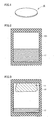
- Fig. 1 is a perspective view schematically showing an SiC crystal 10 in an embodiment of the present invention. Initially, SiC crystal 10 in one embodiment of the present invention will be described with reference to Fig. 1 .
- SiC crystal 10 is, for example, a substrate having a circular two-dimensional shape.
- SiC crystal 10 contains Fe at concentration not higher than 0.1 ppm and Al at concentration not higher than 100 ppm. Lower concentration of Fe and Al is preferred, however, from a point of view of ease of realization, Fe concentration is, for example, not lower than 0.002 ppm and Al concentration is, for example, 0.02 ppm. As concentration of Fe and Al is thus lowered, increase in micropipe density or etch pit density can effectively be suppressed and variation in resistivity can also effectively be suppressed. Concentration of Fe and Al is a value measured, for example, with ICP-AES.
- SiC crystal 10 has micropipe density preferably not higher than 10/cm 2 and more preferably not higher than 2/cm 2 .
- Micropipe density is a value determined, for example, from the number of threading hollow defects counted in a surface etched by immersion in a potassium hydroxide (KOH) melt at 500°C for 1 to 10 minutes, by using a Nomarski differential interference microscope.
- KOH potassium hydroxide
- SiC crystal 10 has etch pit density preferably not higher than 10000/cm 2 and more preferably not higher than 9300/cm 2 .
- Etch pit density is a value determined, for example, from the number of etch pits counted in a surface etched by immersion in a KOH melt at 500°C for 1 to 10 minutes, by using a Nomarski differential interference microscope.
- SiC crystal 10 is preferably a single crystal. Though a polytype of SiC crystal 10 is not particularly limited, for example, 4H-SiC is preferred.
- SiC crystal 10 is manufactured with a sublimation method.
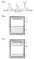
- Figs. 2, 3 , 5, and 6 are each a cross-sectional view schematically showing a process for manufacturing an SiC crystal in the present embodiment.
- Fig. 4 is a diagram for illustrating size distribution of a second source material in the present embodiment.
- the manufacturing apparatus includes a crucible 101 and a heating portion (not shown) for heating crucible 101.
- the heating portion is arranged, for example, around an outer circumference of crucible 101.
- crucible 101 has a lower portion for holding a source material and an upper portion functioning as a cover of the lower portion for holding the source material.
- Crucible 101 is made, for example, of graphite.
- the manufacturing apparatus may include various elements other than the above, for the sake of convenience of description, illustration and description of these elements will not be provided.
- SiC powders for polishing are prepared as a first source material 17.
- GC SiC powders for polishing
- a first SiC crystal 11 is grown by sublimation of first source material 17 through heating and precipitation from a gas of first source material 17.
- a seed substrate In growing first SiC crystal 11 by using GC as a source material, it is preferred not to arrange a seed substrate.
- first source material 17 is heated by the heating portion at a temperature at which first source material 17 sublimates. As a result of this heating, first source material 17 sublimates and a sublimation gas is generated. This sublimation gas is again solidified at a position opposed to the first source material in crucible 101, that is, in the upper portion of crucible 101, that is set at a temperature lower than first source material 17.
- first source material 17 is held at a temperature from 2000°C to 3000°C, and a position opposed to first source material 17 is held at a temperature from 1900°C to 2200°C, which is lower than a temperature of first source material 17.
- an atmospheric pressure in crucible 101 is held preferably at 400 Torr or lower.
- first SiC crystal 11 grows at a position opposed to first source material 17.
- First SiC crystal 11 thus grown is, for example, polycrystalline.
- first source material 17 By setting a temperature of first source material 17 to 2000°C or higher, a growth rate of first SiC crystal 11 can be increased. By setting a temperature of first source material 17 to 3000°C or lower, damage of crucible 101 can be suppressed.
- a growing temperature may be held at a constant temperature during growth, however, it may also be varied at a certain rate during growth.
- a second source material 12 (see Fig. 5 ) is formed by crushing first SiC crystal 11.
- first SiC crystal 11 for example, the following are performed. Specifically, the inside of crucible 101 is cooled to a room temperature. Then, grown first SiC crystal 11 is taken out of crucible 101. This first SiC crystal 11 is crushed, for example, with a crusher. It is noted that a crushing method is not particularly limited.
- second source material 12 is preferably formed such that a plurality of (in Fig. 4 , three peaks A, B and C) size distribution peaks are present in a range not smaller than 1 ⁇ m and not greater than 3 mm and 95% or more particles are present in a range of ⁇ 50% from respective centers A 1, B1 and C1 of size distribution peaks A, B and C.
- centers A1, B1 and C1 of size distribution peaks A, B and C are not smaller than 1 ⁇ m and not greater than 3 mm and 95% or more particles are present in the range of ⁇ 50% from respective centers A1, B1 and C1 of size distribution peaks A, B and C, a filling factor at the time when crucible 101 is filled with second source material 12 can be increased.
- a time period for growth in growing a second SiC crystal 14 by using this second source material 12 is shortened and influence on concentration of a gas of second source material 12 that sublimated during growth can be suppressed. Therefore, quality of second SiC crystal 14 grown by using this second source material 12 can be enhanced.
- second source material 12 is formed such that center A1 of smallest grain size peak A is present in a range not smaller than 1 ⁇ m and not greater than 100 ⁇ m and center C1 of largest grain size peak C is present in a range not smaller than 200 ⁇ m and not greater than 3 mm.
- second source material 12 that peak A includes particles not less than 10 weight % and not more than 50 weight %, peak C includes particles not less than 30 weight % and not more than 80 weight %, and the remainder represents other peak (in Fig. 4 , peak B) is further preferably formed.
- the phrase above that "95% or more particles are present in a range of ⁇ 50% from respective centers A1, B1 and C1 of size distribution peaks A, B and C" means that 95% or more of the whole particles of second source material 12 is present between 150% particle sizes A2, B2 and C2 with respect to particle sizes at centers A1, B1 and C1 and 50% particle sizes A3, B3 and C3 with respect to particle sizes at centers A1, B1 and C1, respectively. It is noted that the number of particle size distribution peaks may be two, or four or more.
- size distribution is a value, for example, determined in conformity with JIS R6001 1998.
- second source material 12 can be formed, for example, by crushing first SiC crystal 11 and thereafter making selection so as to achieve size distribution in the range above. It is noted that second source material 12 may be formed by crushing first SiC crystal 11 so as to have size distribution as above.
- crushed first SiC crystal 11 is preferably washed with an acid solution.
- an acid solution is not particularly limited, aqua regia is preferably used.
- an acid solution in particular aqua regia, such a heavy metal as Fe attached to first SiC crystal 11 during crushing can be removed.
- washing, for example, with hydrochloric acid is further preferred.
- Second source material 12 formed as above preferably contains Fe at concentration not higher than 0.1 ppm and Al at concentration not higher than 100 ppm. In addition, second source material 12 formed as above is placed in the lower portion of crucible 101.
- a seed substrate 13 is arranged in the upper portion of crucible 101 so as to be opposed to second source material 12 in crucible 101.
- a main surface of seed substrate 13 may have a circular or quadrangular shape.
- a material for seed substrate 13 is not particularly limited, from a point of view of enhancing quality of grown second SiC crystal 14, an SiC substrate is preferred and the material is more preferably identical in grown polytype (crystal polymorphism), which means that, for example, in a case where an SiC crystal intended to be grown is 4H-SiC, seed substrate 13 is also 4H-SiC. It is noted that this step may be omitted.
- second SiC crystal 14 is grown by sublimation of second source material 12 through heating and precipitation from a gas of second source material 12.
- second SiC crystal 14 is grown on seed substrate 13.
- Second SiC crystal 14 is preferably a single crystal. Since a method of growing second SiC crystal 14 is substantially the same as the method of growing first SiC crystal 11, description thereof will not be repeated.
- SiC crystal 10 in Fig. 1 may be manufactured by growing first SiC crystal 11 by using first source material 17, forming second source material 12 by crushing first SiC crystal 11, and growing second SiC crystal 14 by using second source material 12.
- the step above is preferably repeated. Namely, the step of forming a third source material by crushing second SiC crystal 14 and the step of growing a third SiC crystal by sublimation of the third source material through heating and precipitation from a gas of the third source material are preferably further performed.
- the steps in this one cycle can decrease impurities, for example, by approximately 10%.
- an SiC crystal is further preferably manufactured by repeating the steps above until a source material having Fe concentration not higher than 0.1 ppm and Al concentration not higher than 100 ppm can be fabricated and by growing an SiC crystal by using this source material.
- an ingot including a seed substrate and an SiC crystal formed on the seed substrate can be manufactured.
- This ingot may be employed as SiC crystal 10 shown in Fig. 1 .
- SiC crystal 10 shown in Fig. 1 may be manufactured by removing seed substrate 13 from the ingot. In a case of removal, only seed substrate 13 may be removed or seed substrate 13 and a part of the grown SiC crystal may be removed.
- a removal method is not particularly limited, and for example, such a mechanical removal method as cutting, grinding and cleavage can be employed.
- Cutting refers to mechanical removal of at least seed substrate 13 from an ingot, for example, by using a wire saw.
- Grinding refers to grinding in a direction of thickness by bringing a grindstone into contact with a surface while it is rotating.
- Cleavage refers to division of a crystal along a crystal lattice plane. It is noted that such a chemical removal method as etching may be employed.
- SiC crystal 10 shown in Fig. 1 may be manufactured by cutting a plurality of SiC crystal slices from the grown SiC crystal. In this case, cost for manufacturing one slice of SiC crystal 10 can be lowered.
- one surface or opposing surfaces of an SiC crystal may be planarized by grinding, polishing or the like, as necessary.
- a method of manufacturing SiC crystal 10 in the embodiment of the present invention includes the steps of preparing SiC powders for polishing as first source material 17, growing first SiC crystal 11 by sublimating first source material 17 through heating and precipitating an SiC crystal, forming second source material 12 by crushing first SiC crystal 11, and growing second SiC crystal 14 by sublimating second source material 12 through heating and precipitating an SiC crystal.
- the present inventor conceived that, by fabricating second source material 12 by crushing first SiC crystal 11 grown with the use of first source material 17 and growing second SiC crystal 14 by using second source material 12, second SiC crystal 14 can contain impurities such as Fe and Al less than first SiC crystal 11.
- first SiC crystal 11 is grown by using a GC source material as first source material 17
- second source material 12 is formed by crushing this first SiC crystal 11
- second SiC crystal 14 is grown by using second source material 12. Therefore, even with the use of GC high in concentration of Fe and Al as a starting source material, second SiC crystal 14 can be lower in impurity concentration than first SiC crystal 11. Therefore, lowering in quality due to impurities in manufactured SiC crystal 10 can be lessened.
- SiC crystal 10 can be manufactured with lower cost.
- SiC crystal 10 having Fe concentration not higher than 0.1 ppm and Al concentration not higher than 100 ppm can be manufactured.
- the present inventor conducted dedicated studies about to which range concentration of Fe and Al impurities in SiC crystal 10 should be lowered to lessen influence on quality due to these impurities. Consequently, the present inventor found that influence on quality of SiC crystal 10 (for example, crystal defects such as micropipes or etch pits) can be lessened by decreasing Fe and Al to the range above. Therefore, according to SiC crystal 10 in the present embodiment, lowering in quality can be suppressed.
- Comparative Example A an SiC crystal was manufactured basically in accordance with the method of manufacturing an SiC crystal in the embodiment described above.
- first source material 17 generally commercially available GC for abrasive was prepared as first source material 17.
- This first source material was arranged in the lower portion of crucible 101 as shown Fig. 2 , while nothing was arranged in a cover of crucible 101 opposed to an outermost surface of first source material 17.
- first SiC crystal 11 was grown by sublimation of first source material 17 through heating and precipitation of a gas of first source material 17.
- a temperature of the lower portion of crucible 101, that is, first source material 17 was set to 2300°C
- a temperature of the upper portion of crucible 101 was set to 2000°C
- a pressure in crucible 101 was set to 1 Torr.
- Grown first SiC crystal 11 was polycrystalline.
- first SiC crystal 11 was crushed. Crushing was carried out by using a crusher. Thereafter, crushed first SiC crystal 11 was washed with aqua regia and further washed with hydrochloric acid. Then, second source material 12 was formed by using crushed first SiC crystal 11 such that there are three size distribution peaks A, B and C, the center of smallest grain size peak A was less than 1 ⁇ m, and the center of largest grain size peak C exceeded 3 mm, as shown in Fig. 4 . In addition, second source material 12 was formed such that 95% or more particles were present in the range of ⁇ 50% from the center of each size distribution peak. Size distribution of second source material 12 was determined in conformity with JIS R6001 1998. This second source material 12 was arranged in the lower portion in crucible 101.
- seed substrate 13 4H-SiC having micropipe density of 10/cm 2 was prepared as seed substrate 13. This seed substrate 13 was arranged in the upper portion in crucible 101 to be opposed to second source material 12.
- second SiC crystal 14 was grown by sublimation of second source material 12 through heating and precipitation of a gas of second source material 12.
- the method of growing second SiC crystal 14 was the same as the method of growing first SiC crystal 11.
- a method of manufacturing an SiC crystal in Comparative Example B was basically the same as in Comparative Example A, however, it was different in that second source material 12 of which center of largest grain size peak C was not smaller than 200 ⁇ m and not greater than 3 mm was formed in the step of forming second source material 12.
- a method of manufacturing an SiC crystal in Comparative Example C was basically the same as in Comparative Example A, however, it was different in that second source material 12 of which center of smallest grain size peak A was not smaller than 1 ⁇ m and not greater than 100 ⁇ m was formed in the step of forming second source material 12.
- a method of manufacturing an SiC crystal in Present Inventive Example 4 was basically the same as in Comparative Example A, however, it was different in that second source material 12 of which center of smallest grain size peak A was not smaller than 1 ⁇ m and not greater than 100 ⁇ m and of which center of largest grain size peak C was not smaller than 200 ⁇ m and not greater than 3 mm was formed in the step of forming second source material 12.
- a method of manufacturing an SiC crystal in Comparative Example D was basically the same as in Comparative Example A, however, it was different in that the step of forming a second source material by crushing first SiC crystal 11 was not performed. Namely, first SiC crystal 11 was adopted as the SiC crystal in Comparative Example D.
- Al and Fe concentrations were determined with ICP (Inductive Coupled Plasma)-AES (Atomic Emission Spectrometry). It is noted that Al detection limit was 0.02 ppm and Fe detection limit was 0.002 ppm.
- Micropipe density was determined based on the number of threading hollow defects in an etched surface of an SiC crystal counted by using a Nomarski differential interference microscope, after the SiC crystals in the Present Inventive Example and Comparative Examples A to D were sliced to have a plane distant by 10 mm from a plane in contact with seed substrate 13 and immersed in a KOH melt at 500°C for 1 to 10 minutes.
- micropipe density of the SiC crystal grown on seed substrate 13 with respect to micropipe density of seed substrate 13 (MPD of crystal/MPD of seed substrate in Table 1) was also calculated.
- Etch pit density was determined based on the number of etch pits in an etched surface of an SiC crystal counted by using a Nomarski differential interference microscope, after the SiC crystals in the Present Inventive Example and Comparative Examples A to D were sliced to have a plane distant by 10 mm from a plane in contact with seed substrate 13 and immersed in a KOH melt at 500°C for I to 10 minutes.
- the Present Inventive Example-4 in which the second source material was formed in the step of forming a second source material such that there were a plurality of size distribution peaks in the range not smaller than 1 ⁇ m and not greater than 3 mm and 95% or more particles were present in the range of ⁇ 50% from the center of each size distribution peak could be further lower in micropipe density and etch pit density than Comparative Examples 1 to 3. Furthermore, it was also found that takeover of micropipes in seed substrate 13 was further less.
Landscapes
- Chemical & Material Sciences (AREA)
- Engineering & Computer Science (AREA)
- Crystallography & Structural Chemistry (AREA)
- Materials Engineering (AREA)
- Metallurgy (AREA)
- Organic Chemistry (AREA)
- Inorganic Chemistry (AREA)
- Crystals, And After-Treatments Of Crystals (AREA)
- Physical Deposition Of Substances That Are Components Of Semiconductor Devices (AREA)
- Carbon And Carbon Compounds (AREA)
Applications Claiming Priority (2)
| Application Number | Priority Date | Filing Date | Title |
|---|---|---|---|
| JP2010100891A JP5565070B2 (ja) | 2010-04-26 | 2010-04-26 | 炭化珪素結晶および炭化珪素結晶の製造方法 |
| PCT/JP2011/054339 WO2011135913A1 (ja) | 2010-04-26 | 2011-02-25 | 炭化珪素結晶および炭化珪素結晶の製造方法 |
Publications (3)
| Publication Number | Publication Date |
|---|---|
| EP2565301A1 EP2565301A1 (en) | 2013-03-06 |
| EP2565301A4 EP2565301A4 (en) | 2013-11-27 |
| EP2565301B1 true EP2565301B1 (en) | 2015-03-25 |
Family
ID=44861234
Family Applications (1)
| Application Number | Title | Priority Date | Filing Date |
|---|---|---|---|
| EP11774697.4A Active EP2565301B1 (en) | 2010-04-26 | 2011-02-25 | Silicon carbide crystal and method for producing silicon carbide crystal |
Country Status (8)
| Country | Link |
|---|---|
| US (3) | US8574529B2 (https=) |
| EP (1) | EP2565301B1 (https=) |
| JP (1) | JP5565070B2 (https=) |
| KR (1) | KR20120130318A (https=) |
| CN (1) | CN102597339A (https=) |
| CA (1) | CA2775923A1 (https=) |
| TW (1) | TW201142092A (https=) |
| WO (1) | WO2011135913A1 (https=) |
Families Citing this family (9)
| Publication number | Priority date | Publication date | Assignee | Title |
|---|---|---|---|---|
| JP5910393B2 (ja) | 2012-07-26 | 2016-04-27 | 住友電気工業株式会社 | 炭化珪素基板の製造方法 |
| JP6028754B2 (ja) | 2014-03-11 | 2016-11-16 | トヨタ自動車株式会社 | SiC単結晶基板の製造方法 |
| US10108798B1 (en) * | 2016-01-04 | 2018-10-23 | Smart Information Flow Technologies LLC | Methods and systems for defending against cyber-attacks |
| CN105603530B (zh) * | 2016-01-12 | 2018-02-27 | 台州市一能科技有限公司 | 用于碳化硅晶体高速生长的原料及碳化硅晶体的生长方法 |
| JP6086167B2 (ja) * | 2016-03-18 | 2017-03-01 | 住友電気工業株式会社 | 炭化珪素基板の製造方法 |
| WO2018176302A1 (zh) * | 2017-03-30 | 2018-10-04 | 新疆天科合达蓝光半导体有限公司 | 用于生长SiC晶体的SiC原料的制备方法和制备装置 |
| CN115704110A (zh) * | 2021-08-06 | 2023-02-17 | 株式会社电装 | 碳化硅晶体制造设备、其控制装置及生成学习模型和控制其的方法 |
| KR102442731B1 (ko) | 2021-12-23 | 2022-09-13 | 주식회사 쎄닉 | 탄화규소 분말 및 이를 이용하여 탄화규소 잉곳을 제조하는 방법 |
| KR102442730B1 (ko) * | 2021-12-23 | 2022-09-13 | 주식회사 쎄닉 | 탄화규소 분말, 이를 이용하여 탄화규소 잉곳을 제조하는 방법 및 탄화규소 웨이퍼 |
Family Cites Families (19)
| Publication number | Priority date | Publication date | Assignee | Title |
|---|---|---|---|---|
| JPS58147493A (ja) | 1982-02-12 | 1983-09-02 | フイリツプス・ペトロリユ−ム・コンパニ− | 熱分解法用の防汚剤 |
| JPS58187479A (ja) | 1982-04-27 | 1983-11-01 | Honda Motor Co Ltd | 可撓シ−ル材の外被材貼付方法 |
| JPH0645519B2 (ja) * | 1986-08-18 | 1994-06-15 | 三洋電機株式会社 | p型SiC単結晶の成長方法 |
| JPS6350393A (ja) * | 1986-08-20 | 1988-03-03 | Sanyo Electric Co Ltd | SiC単結晶の成長方法 |
| JP3934695B2 (ja) * | 1995-05-31 | 2007-06-20 | 株式会社ブリヂストン | 炭化ケイ素単結晶製造用高純度炭化ケイ素粉体の製造方法 |
| US5863325A (en) | 1995-05-31 | 1999-01-26 | Bridgestone Corporation | Process for producing high purity silicon carbide powder for preparation of a silicon carbide single crystal and single crystal |
| JP3590464B2 (ja) | 1995-12-08 | 2004-11-17 | 新日本製鐵株式会社 | 4h型単結晶炭化珪素の製造方法 |
| US7553373B2 (en) * | 2001-06-15 | 2009-06-30 | Bridgestone Corporation | Silicon carbide single crystal and production thereof |
| SE520968C2 (sv) * | 2001-10-29 | 2003-09-16 | Okmetic Oyj | Högresistiv monokristallin kiselkarbid och metod för dess framställning |
| JP4593099B2 (ja) * | 2003-03-10 | 2010-12-08 | 学校法人関西学院 | 単結晶炭化ケイ素の液相エピタキシャル成長法及びそれに用いられる熱処理装置 |
| US20060249073A1 (en) | 2003-03-10 | 2006-11-09 | The New Industry Research Organization | Method of heat treatment and heat treatment apparatus |
| JP4307913B2 (ja) | 2003-06-18 | 2009-08-05 | 新日本製鐵株式会社 | 高純度炭化珪素単結晶の製造方法 |
| JP2005239496A (ja) * | 2004-02-27 | 2005-09-08 | Nippon Steel Corp | 炭化珪素単結晶育成用炭化珪素原料と炭化珪素単結晶及びその製造方法 |
| JP4427470B2 (ja) | 2004-03-29 | 2010-03-10 | 新日本製鐵株式会社 | 炭化珪素単結晶の製造方法 |
| WO2006017074A2 (en) * | 2004-07-07 | 2006-02-16 | Ii-Vi Incorporated | Low-doped semi-insulating sic crystals and method |
| JP2007284306A (ja) * | 2006-04-19 | 2007-11-01 | Nippon Steel Corp | 炭化珪素単結晶及びその製造方法 |
| CN101536168A (zh) * | 2006-09-14 | 2009-09-16 | 科锐有限公司 | 无微管碳化硅及其相关制备方法 |
| JP2010083681A (ja) * | 2008-09-29 | 2010-04-15 | Bridgestone Corp | 炭化ケイ素単結晶の製造方法及び真空チャック |
| JP2010095397A (ja) * | 2008-10-15 | 2010-04-30 | Nippon Steel Corp | 炭化珪素単結晶及び炭化珪素単結晶ウェハ |
-
2010
- 2010-04-26 JP JP2010100891A patent/JP5565070B2/ja active Active
-
2011
- 2011-02-25 EP EP11774697.4A patent/EP2565301B1/en active Active
- 2011-02-25 CN CN2011800043891A patent/CN102597339A/zh active Pending
- 2011-02-25 WO PCT/JP2011/054339 patent/WO2011135913A1/ja not_active Ceased
- 2011-02-25 CA CA2775923A patent/CA2775923A1/en not_active Abandoned
- 2011-02-25 US US13/499,482 patent/US8574529B2/en active Active
- 2011-02-25 KR KR1020127009040A patent/KR20120130318A/ko not_active Ceased
- 2011-04-15 TW TW100113266A patent/TW201142092A/zh unknown
-
2013
- 2013-09-06 US US14/019,882 patent/US20140004303A1/en not_active Abandoned
-
2016
- 2016-06-17 US US15/185,602 patent/US9725823B2/en active Active
Also Published As
| Publication number | Publication date |
|---|---|
| US20120183466A1 (en) | 2012-07-19 |
| US20160289863A1 (en) | 2016-10-06 |
| US9725823B2 (en) | 2017-08-08 |
| WO2011135913A1 (ja) | 2011-11-03 |
| EP2565301A4 (en) | 2013-11-27 |
| EP2565301A1 (en) | 2013-03-06 |
| TW201142092A (en) | 2011-12-01 |
| CA2775923A1 (en) | 2011-11-03 |
| CN102597339A (zh) | 2012-07-18 |
| KR20120130318A (ko) | 2012-11-30 |
| JP2011230941A (ja) | 2011-11-17 |
| US20140004303A1 (en) | 2014-01-02 |
| JP5565070B2 (ja) | 2014-08-06 |
| US8574529B2 (en) | 2013-11-05 |
Similar Documents
| Publication | Publication Date | Title |
|---|---|---|
| EP2565301B1 (en) | Silicon carbide crystal and method for producing silicon carbide crystal | |
| JP6584428B2 (ja) | 炭化珪素単結晶の製造方法及び炭化珪素単結晶基板 | |
| JP5706823B2 (ja) | SiC単結晶ウエハーとその製造方法 | |
| CN103620095B (zh) | 碳化硅单晶基板及其制造方法 | |
| JP5402701B2 (ja) | 炭化珪素結晶の製造方法 | |
| JP7747730B2 (ja) | 高品質の炭化ケイ素種結晶、炭化ケイ素結晶、炭化ケイ素基板およびそれらの製造方法 | |
| JP2025019098A (ja) | 結晶学的応力が低減した大寸法炭化ケイ素単結晶材料 | |
| JP6624868B2 (ja) | p型低抵抗率炭化珪素単結晶基板 | |
| EP2921575A1 (en) | Silicon carbide single crystal substrate and process for producing same | |
| JP2017065986A (ja) | 低抵抗率炭化珪素単結晶基板の製造方法 | |
| CN105189836A (zh) | β-Ga2O3系单晶的培养方法、以及β-Ga2O3系单晶基板及其制造方法 | |
| CN113322519B (zh) | 晶片的制造方法 | |
| JP2004099340A (ja) | 炭化珪素単結晶育成用種結晶と炭化珪素単結晶インゴット及びその製造方法 | |
| EP4105367A1 (en) | Silicon carbide wafer and semiconductor device | |
| JP2012250897A (ja) | 単結晶炭化珪素基板およびその製造方法 | |
| US20110217224A1 (en) | Silicon carbide crystal, method of manufacturing the same, apparatus for manufacturing the same, and crucible | |
| JP4585359B2 (ja) | 炭化珪素単結晶の製造方法 | |
| JP4494856B2 (ja) | 炭化珪素単結晶成長用種結晶とその製造方法及びそれを用いた結晶成長方法 | |
| JP5135545B2 (ja) | 炭化珪素単結晶インゴット育成用種結晶及びその製造方法 | |
| JP2022062043A (ja) | ウエハの製造方法、エピタキシャルウエハの製造方法、これによって製造されたウエハ及びエピタキシャルウエハ | |
| KR102236397B1 (ko) | 탄화규소 웨이퍼 및 이를 적용한 반도체 소자 | |
| JP6628557B2 (ja) | 炭化珪素単結晶の製造方法 | |
| JP2014015394A (ja) | 炭化珪素結晶の製造方法 |
Legal Events
| Date | Code | Title | Description |
|---|---|---|---|
| PUAI | Public reference made under article 153(3) epc to a published international application that has entered the european phase |
Free format text: ORIGINAL CODE: 0009012 |
|
| 17P | Request for examination filed |
Effective date: 20120327 |
|
| AK | Designated contracting states |
Kind code of ref document: A1 Designated state(s): AL AT BE BG CH CY CZ DE DK EE ES FI FR GB GR HR HU IE IS IT LI LT LU LV MC MK MT NL NO PL PT RO RS SE SI SK SM TR |
|
| DAX | Request for extension of the european patent (deleted) | ||
| A4 | Supplementary search report drawn up and despatched |
Effective date: 20131025 |
|
| RIC1 | Information provided on ipc code assigned before grant |
Ipc: H01L 21/203 20060101ALI20131021BHEP Ipc: H01L 21/02 20060101ALI20131021BHEP Ipc: C30B 23/06 20060101ALI20131021BHEP Ipc: C30B 23/00 20060101ALI20131021BHEP Ipc: C30B 29/36 20060101AFI20131021BHEP |
|
| 17Q | First examination report despatched |
Effective date: 20140704 |
|
| GRAP | Despatch of communication of intention to grant a patent |
Free format text: ORIGINAL CODE: EPIDOSNIGR1 |
|
| RIC1 | Information provided on ipc code assigned before grant |
Ipc: C30B 23/02 20060101ALI20140829BHEP Ipc: C30B 35/00 20060101ALI20140829BHEP Ipc: C30B 23/00 20060101ALI20140829BHEP Ipc: C30B 23/06 20060101ALI20140829BHEP Ipc: C30B 29/36 20060101AFI20140829BHEP Ipc: H01L 21/203 20060101ALI20140829BHEP Ipc: H01L 21/02 20060101ALI20140829BHEP |
|
| INTG | Intention to grant announced |
Effective date: 20140930 |
|
| GRAS | Grant fee paid |
Free format text: ORIGINAL CODE: EPIDOSNIGR3 |
|
| GRAA | (expected) grant |
Free format text: ORIGINAL CODE: 0009210 |
|
| AK | Designated contracting states |
Kind code of ref document: B1 Designated state(s): AL AT BE BG CH CY CZ DE DK EE ES FI FR GB GR HR HU IE IS IT LI LT LU LV MC MK MT NL NO PL PT RO RS SE SI SK SM TR |
|
| REG | Reference to a national code |
Ref country code: GB Ref legal event code: FG4D |
|
| REG | Reference to a national code |
Ref country code: CH Ref legal event code: EP |
|
| REG | Reference to a national code |
Ref country code: IE Ref legal event code: FG4D |
|
| REG | Reference to a national code |
Ref country code: DE Ref legal event code: R096 Ref document number: 602011015081 Country of ref document: DE Effective date: 20150507 |
|
| REG | Reference to a national code |
Ref country code: AT Ref legal event code: REF Ref document number: 717947 Country of ref document: AT Kind code of ref document: T Effective date: 20150515 |
|
| REG | Reference to a national code |
Ref country code: SE Ref legal event code: TRGR |
|
| PG25 | Lapsed in a contracting state [announced via postgrant information from national office to epo] |
Ref country code: FI Free format text: LAPSE BECAUSE OF FAILURE TO SUBMIT A TRANSLATION OF THE DESCRIPTION OR TO PAY THE FEE WITHIN THE PRESCRIBED TIME-LIMIT Effective date: 20150325 Ref country code: HR Free format text: LAPSE BECAUSE OF FAILURE TO SUBMIT A TRANSLATION OF THE DESCRIPTION OR TO PAY THE FEE WITHIN THE PRESCRIBED TIME-LIMIT Effective date: 20150325 Ref country code: LT Free format text: LAPSE BECAUSE OF FAILURE TO SUBMIT A TRANSLATION OF THE DESCRIPTION OR TO PAY THE FEE WITHIN THE PRESCRIBED TIME-LIMIT Effective date: 20150325 |
|
| REG | Reference to a national code |
Ref country code: AT Ref legal event code: MK05 Ref document number: 717947 Country of ref document: AT Kind code of ref document: T Effective date: 20150325 |
|
| REG | Reference to a national code |
Ref country code: LT Ref legal event code: MG4D |
|
| PG25 | Lapsed in a contracting state [announced via postgrant information from national office to epo] |
Ref country code: RS Free format text: LAPSE BECAUSE OF FAILURE TO SUBMIT A TRANSLATION OF THE DESCRIPTION OR TO PAY THE FEE WITHIN THE PRESCRIBED TIME-LIMIT Effective date: 20150325 Ref country code: LV Free format text: LAPSE BECAUSE OF FAILURE TO SUBMIT A TRANSLATION OF THE DESCRIPTION OR TO PAY THE FEE WITHIN THE PRESCRIBED TIME-LIMIT Effective date: 20150325 Ref country code: GR Free format text: LAPSE BECAUSE OF FAILURE TO SUBMIT A TRANSLATION OF THE DESCRIPTION OR TO PAY THE FEE WITHIN THE PRESCRIBED TIME-LIMIT Effective date: 20150626 |
|
| PG25 | Lapsed in a contracting state [announced via postgrant information from national office to epo] |
Ref country code: NL Free format text: LAPSE BECAUSE OF FAILURE TO SUBMIT A TRANSLATION OF THE DESCRIPTION OR TO PAY THE FEE WITHIN THE PRESCRIBED TIME-LIMIT Effective date: 20150325 |
|
| PG25 | Lapsed in a contracting state [announced via postgrant information from national office to epo] |
Ref country code: EE Free format text: LAPSE BECAUSE OF FAILURE TO SUBMIT A TRANSLATION OF THE DESCRIPTION OR TO PAY THE FEE WITHIN THE PRESCRIBED TIME-LIMIT Effective date: 20150325 Ref country code: SK Free format text: LAPSE BECAUSE OF FAILURE TO SUBMIT A TRANSLATION OF THE DESCRIPTION OR TO PAY THE FEE WITHIN THE PRESCRIBED TIME-LIMIT Effective date: 20150325 Ref country code: CZ Free format text: LAPSE BECAUSE OF FAILURE TO SUBMIT A TRANSLATION OF THE DESCRIPTION OR TO PAY THE FEE WITHIN THE PRESCRIBED TIME-LIMIT Effective date: 20150325 Ref country code: RO Free format text: LAPSE BECAUSE OF FAILURE TO SUBMIT A TRANSLATION OF THE DESCRIPTION OR TO PAY THE FEE WITHIN THE PRESCRIBED TIME-LIMIT Effective date: 20150325 Ref country code: PT Free format text: LAPSE BECAUSE OF FAILURE TO SUBMIT A TRANSLATION OF THE DESCRIPTION OR TO PAY THE FEE WITHIN THE PRESCRIBED TIME-LIMIT Effective date: 20150727 Ref country code: ES Free format text: LAPSE BECAUSE OF FAILURE TO SUBMIT A TRANSLATION OF THE DESCRIPTION OR TO PAY THE FEE WITHIN THE PRESCRIBED TIME-LIMIT Effective date: 20150325 |
|
| PG25 | Lapsed in a contracting state [announced via postgrant information from national office to epo] |
Ref country code: AT Free format text: LAPSE BECAUSE OF FAILURE TO SUBMIT A TRANSLATION OF THE DESCRIPTION OR TO PAY THE FEE WITHIN THE PRESCRIBED TIME-LIMIT Effective date: 20150325 Ref country code: IS Free format text: LAPSE BECAUSE OF FAILURE TO SUBMIT A TRANSLATION OF THE DESCRIPTION OR TO PAY THE FEE WITHIN THE PRESCRIBED TIME-LIMIT Effective date: 20150725 Ref country code: PL Free format text: LAPSE BECAUSE OF FAILURE TO SUBMIT A TRANSLATION OF THE DESCRIPTION OR TO PAY THE FEE WITHIN THE PRESCRIBED TIME-LIMIT Effective date: 20150325 |
|
| REG | Reference to a national code |
Ref country code: DE Ref legal event code: R097 Ref document number: 602011015081 Country of ref document: DE |
|
| PG25 | Lapsed in a contracting state [announced via postgrant information from national office to epo] |
Ref country code: DK Free format text: LAPSE BECAUSE OF FAILURE TO SUBMIT A TRANSLATION OF THE DESCRIPTION OR TO PAY THE FEE WITHIN THE PRESCRIBED TIME-LIMIT Effective date: 20150325 |
|
| PLBE | No opposition filed within time limit |
Free format text: ORIGINAL CODE: 0009261 |
|
| STAA | Information on the status of an ep patent application or granted ep patent |
Free format text: STATUS: NO OPPOSITION FILED WITHIN TIME LIMIT |
|
| 26N | No opposition filed |
Effective date: 20160105 |
|
| PG25 | Lapsed in a contracting state [announced via postgrant information from national office to epo] |
Ref country code: BE Free format text: LAPSE BECAUSE OF NON-PAYMENT OF DUE FEES Effective date: 20160229 Ref country code: SI Free format text: LAPSE BECAUSE OF FAILURE TO SUBMIT A TRANSLATION OF THE DESCRIPTION OR TO PAY THE FEE WITHIN THE PRESCRIBED TIME-LIMIT Effective date: 20150325 |
|
| PG25 | Lapsed in a contracting state [announced via postgrant information from national office to epo] |
Ref country code: BE Free format text: LAPSE BECAUSE OF FAILURE TO SUBMIT A TRANSLATION OF THE DESCRIPTION OR TO PAY THE FEE WITHIN THE PRESCRIBED TIME-LIMIT Effective date: 20150325 |
|
| PG25 | Lapsed in a contracting state [announced via postgrant information from national office to epo] |
Ref country code: LU Free format text: LAPSE BECAUSE OF FAILURE TO SUBMIT A TRANSLATION OF THE DESCRIPTION OR TO PAY THE FEE WITHIN THE PRESCRIBED TIME-LIMIT Effective date: 20160225 Ref country code: MC Free format text: LAPSE BECAUSE OF FAILURE TO SUBMIT A TRANSLATION OF THE DESCRIPTION OR TO PAY THE FEE WITHIN THE PRESCRIBED TIME-LIMIT Effective date: 20150325 |
|
| REG | Reference to a national code |
Ref country code: CH Ref legal event code: PL |
|
| REG | Reference to a national code |
Ref country code: SE Ref legal event code: EUG |
|
| GBPC | Gb: european patent ceased through non-payment of renewal fee |
Effective date: 20160225 |
|
| PG25 | Lapsed in a contracting state [announced via postgrant information from national office to epo] |
Ref country code: LI Free format text: LAPSE BECAUSE OF NON-PAYMENT OF DUE FEES Effective date: 20160229 Ref country code: CH Free format text: LAPSE BECAUSE OF NON-PAYMENT OF DUE FEES Effective date: 20160229 |
|
| REG | Reference to a national code |
Ref country code: FR Ref legal event code: ST Effective date: 20161028 |
|
| PG25 | Lapsed in a contracting state [announced via postgrant information from national office to epo] |
Ref country code: SE Free format text: LAPSE BECAUSE OF NON-PAYMENT OF DUE FEES Effective date: 20160226 |
|
| REG | Reference to a national code |
Ref country code: IE Ref legal event code: MM4A |
|
| PG25 | Lapsed in a contracting state [announced via postgrant information from national office to epo] |
Ref country code: GB Free format text: LAPSE BECAUSE OF NON-PAYMENT OF DUE FEES Effective date: 20160225 Ref country code: IE Free format text: LAPSE BECAUSE OF NON-PAYMENT OF DUE FEES Effective date: 20160225 Ref country code: FR Free format text: LAPSE BECAUSE OF NON-PAYMENT OF DUE FEES Effective date: 20160229 |
|
| PG25 | Lapsed in a contracting state [announced via postgrant information from national office to epo] |
Ref country code: IT Free format text: LAPSE BECAUSE OF NON-PAYMENT OF DUE FEES Effective date: 20160225 |
|
| PG25 | Lapsed in a contracting state [announced via postgrant information from national office to epo] |
Ref country code: MT Free format text: LAPSE BECAUSE OF FAILURE TO SUBMIT A TRANSLATION OF THE DESCRIPTION OR TO PAY THE FEE WITHIN THE PRESCRIBED TIME-LIMIT Effective date: 20150325 |
|
| PG25 | Lapsed in a contracting state [announced via postgrant information from national office to epo] |
Ref country code: HU Free format text: LAPSE BECAUSE OF FAILURE TO SUBMIT A TRANSLATION OF THE DESCRIPTION OR TO PAY THE FEE WITHIN THE PRESCRIBED TIME-LIMIT; INVALID AB INITIO Effective date: 20110225 Ref country code: CY Free format text: LAPSE BECAUSE OF FAILURE TO SUBMIT A TRANSLATION OF THE DESCRIPTION OR TO PAY THE FEE WITHIN THE PRESCRIBED TIME-LIMIT Effective date: 20150325 Ref country code: SM Free format text: LAPSE BECAUSE OF FAILURE TO SUBMIT A TRANSLATION OF THE DESCRIPTION OR TO PAY THE FEE WITHIN THE PRESCRIBED TIME-LIMIT Effective date: 20150325 |
|
| PG25 | Lapsed in a contracting state [announced via postgrant information from national office to epo] |
Ref country code: NO Free format text: LAPSE BECAUSE OF NON-PAYMENT OF DUE FEES Effective date: 20150625 Ref country code: TR Free format text: LAPSE BECAUSE OF FAILURE TO SUBMIT A TRANSLATION OF THE DESCRIPTION OR TO PAY THE FEE WITHIN THE PRESCRIBED TIME-LIMIT Effective date: 20150325 Ref country code: MT Free format text: LAPSE BECAUSE OF FAILURE TO SUBMIT A TRANSLATION OF THE DESCRIPTION OR TO PAY THE FEE WITHIN THE PRESCRIBED TIME-LIMIT Effective date: 20160229 Ref country code: MK Free format text: LAPSE BECAUSE OF FAILURE TO SUBMIT A TRANSLATION OF THE DESCRIPTION OR TO PAY THE FEE WITHIN THE PRESCRIBED TIME-LIMIT Effective date: 20150325 |
|
| PG25 | Lapsed in a contracting state [announced via postgrant information from national office to epo] |
Ref country code: BG Free format text: LAPSE BECAUSE OF FAILURE TO SUBMIT A TRANSLATION OF THE DESCRIPTION OR TO PAY THE FEE WITHIN THE PRESCRIBED TIME-LIMIT Effective date: 20150325 |
|
| PG25 | Lapsed in a contracting state [announced via postgrant information from national office to epo] |
Ref country code: AL Free format text: LAPSE BECAUSE OF FAILURE TO SUBMIT A TRANSLATION OF THE DESCRIPTION OR TO PAY THE FEE WITHIN THE PRESCRIBED TIME-LIMIT Effective date: 20150325 |
|
| P01 | Opt-out of the competence of the unified patent court (upc) registered |
Effective date: 20230515 |
|
| PGFP | Annual fee paid to national office [announced via postgrant information from national office to epo] |
Ref country code: DE Payment date: 20260102 Year of fee payment: 16 |