WO2011135913A1 - 炭化珪素結晶および炭化珪素結晶の製造方法 - Google Patents
炭化珪素結晶および炭化珪素結晶の製造方法 Download PDFInfo
- Publication number
- WO2011135913A1 WO2011135913A1 PCT/JP2011/054339 JP2011054339W WO2011135913A1 WO 2011135913 A1 WO2011135913 A1 WO 2011135913A1 JP 2011054339 W JP2011054339 W JP 2011054339W WO 2011135913 A1 WO2011135913 A1 WO 2011135913A1
- Authority
- WO
- WIPO (PCT)
- Prior art keywords
- raw material
- sic crystal
- silicon carbide
- crystal
- sic
- Prior art date
- Legal status (The legal status is an assumption and is not a legal conclusion. Google has not performed a legal analysis and makes no representation as to the accuracy of the status listed.)
- Ceased
Links
- 0 *C[C@@](*)CN* Chemical compound *C[C@@](*)CN* 0.000 description 1
Images


Classifications
-
- C—CHEMISTRY; METALLURGY
- C30—CRYSTAL GROWTH
- C30B—SINGLE-CRYSTAL GROWTH; UNIDIRECTIONAL SOLIDIFICATION OF EUTECTIC MATERIAL OR UNIDIRECTIONAL DEMIXING OF EUTECTOID MATERIAL; REFINING BY ZONE-MELTING OF MATERIAL; PRODUCTION OF A HOMOGENEOUS POLYCRYSTALLINE MATERIAL WITH DEFINED STRUCTURE; SINGLE CRYSTALS OR HOMOGENEOUS POLYCRYSTALLINE MATERIAL WITH DEFINED STRUCTURE; AFTER-TREATMENT OF SINGLE CRYSTALS OR A HOMOGENEOUS POLYCRYSTALLINE MATERIAL WITH DEFINED STRUCTURE; APPARATUS THEREFOR
- C30B23/00—Single-crystal growth by condensing evaporated or sublimed materials
- C30B23/02—Epitaxial-layer growth
- C30B23/025—Epitaxial-layer growth characterised by the substrate
-
- C—CHEMISTRY; METALLURGY
- C30—CRYSTAL GROWTH
- C30B—SINGLE-CRYSTAL GROWTH; UNIDIRECTIONAL SOLIDIFICATION OF EUTECTIC MATERIAL OR UNIDIRECTIONAL DEMIXING OF EUTECTOID MATERIAL; REFINING BY ZONE-MELTING OF MATERIAL; PRODUCTION OF A HOMOGENEOUS POLYCRYSTALLINE MATERIAL WITH DEFINED STRUCTURE; SINGLE CRYSTALS OR HOMOGENEOUS POLYCRYSTALLINE MATERIAL WITH DEFINED STRUCTURE; AFTER-TREATMENT OF SINGLE CRYSTALS OR A HOMOGENEOUS POLYCRYSTALLINE MATERIAL WITH DEFINED STRUCTURE; APPARATUS THEREFOR
- C30B23/00—Single-crystal growth by condensing evaporated or sublimed materials
- C30B23/02—Epitaxial-layer growth
- C30B23/06—Heating of the deposition chamber, the substrate or the materials to be evaporated
-
- C—CHEMISTRY; METALLURGY
- C30—CRYSTAL GROWTH
- C30B—SINGLE-CRYSTAL GROWTH; UNIDIRECTIONAL SOLIDIFICATION OF EUTECTIC MATERIAL OR UNIDIRECTIONAL DEMIXING OF EUTECTOID MATERIAL; REFINING BY ZONE-MELTING OF MATERIAL; PRODUCTION OF A HOMOGENEOUS POLYCRYSTALLINE MATERIAL WITH DEFINED STRUCTURE; SINGLE CRYSTALS OR HOMOGENEOUS POLYCRYSTALLINE MATERIAL WITH DEFINED STRUCTURE; AFTER-TREATMENT OF SINGLE CRYSTALS OR A HOMOGENEOUS POLYCRYSTALLINE MATERIAL WITH DEFINED STRUCTURE; APPARATUS THEREFOR
- C30B23/00—Single-crystal growth by condensing evaporated or sublimed materials
- C30B23/02—Epitaxial-layer growth
-
- C—CHEMISTRY; METALLURGY
- C30—CRYSTAL GROWTH
- C30B—SINGLE-CRYSTAL GROWTH; UNIDIRECTIONAL SOLIDIFICATION OF EUTECTIC MATERIAL OR UNIDIRECTIONAL DEMIXING OF EUTECTOID MATERIAL; REFINING BY ZONE-MELTING OF MATERIAL; PRODUCTION OF A HOMOGENEOUS POLYCRYSTALLINE MATERIAL WITH DEFINED STRUCTURE; SINGLE CRYSTALS OR HOMOGENEOUS POLYCRYSTALLINE MATERIAL WITH DEFINED STRUCTURE; AFTER-TREATMENT OF SINGLE CRYSTALS OR A HOMOGENEOUS POLYCRYSTALLINE MATERIAL WITH DEFINED STRUCTURE; APPARATUS THEREFOR
- C30B29/00—Single crystals or homogeneous polycrystalline material with defined structure characterised by the material or by their shape
- C30B29/10—Inorganic compounds or compositions
- C30B29/36—Carbides
-
- C—CHEMISTRY; METALLURGY
- C30—CRYSTAL GROWTH
- C30B—SINGLE-CRYSTAL GROWTH; UNIDIRECTIONAL SOLIDIFICATION OF EUTECTIC MATERIAL OR UNIDIRECTIONAL DEMIXING OF EUTECTOID MATERIAL; REFINING BY ZONE-MELTING OF MATERIAL; PRODUCTION OF A HOMOGENEOUS POLYCRYSTALLINE MATERIAL WITH DEFINED STRUCTURE; SINGLE CRYSTALS OR HOMOGENEOUS POLYCRYSTALLINE MATERIAL WITH DEFINED STRUCTURE; AFTER-TREATMENT OF SINGLE CRYSTALS OR A HOMOGENEOUS POLYCRYSTALLINE MATERIAL WITH DEFINED STRUCTURE; APPARATUS THEREFOR
- C30B35/00—Apparatus not otherwise provided for, specially adapted for the growth, production or after-treatment of single crystals or of a homogeneous polycrystalline material with defined structure
- C30B35/007—Apparatus for preparing, pre-treating the source material to be used for crystal growth
-
- H—ELECTRICITY
- H10—SEMICONDUCTOR DEVICES; ELECTRIC SOLID-STATE DEVICES NOT OTHERWISE PROVIDED FOR
- H10P—GENERIC PROCESSES OR APPARATUS FOR THE MANUFACTURE OR TREATMENT OF DEVICES COVERED BY CLASS H10
- H10P14/00—Formation of materials, e.g. in the shape of layers or pillars
- H10P14/20—Formation of materials, e.g. in the shape of layers or pillars of semiconductor materials
- H10P14/22—Formation of materials, e.g. in the shape of layers or pillars of semiconductor materials using physical deposition, e.g. vacuum deposition or sputtering
-
- H—ELECTRICITY
- H10—SEMICONDUCTOR DEVICES; ELECTRIC SOLID-STATE DEVICES NOT OTHERWISE PROVIDED FOR
- H10P—GENERIC PROCESSES OR APPARATUS FOR THE MANUFACTURE OR TREATMENT OF DEVICES COVERED BY CLASS H10
- H10P14/00—Formation of materials, e.g. in the shape of layers or pillars
- H10P14/20—Formation of materials, e.g. in the shape of layers or pillars of semiconductor materials
- H10P14/29—Formation of materials, e.g. in the shape of layers or pillars of semiconductor materials characterised by the substrates
- H10P14/2901—Materials
- H10P14/2902—Materials being Group IVA materials
- H10P14/2904—Silicon carbide
-
- H—ELECTRICITY
- H10—SEMICONDUCTOR DEVICES; ELECTRIC SOLID-STATE DEVICES NOT OTHERWISE PROVIDED FOR
- H10P—GENERIC PROCESSES OR APPARATUS FOR THE MANUFACTURE OR TREATMENT OF DEVICES COVERED BY CLASS H10
- H10P14/00—Formation of materials, e.g. in the shape of layers or pillars
- H10P14/20—Formation of materials, e.g. in the shape of layers or pillars of semiconductor materials
- H10P14/34—Deposited materials, e.g. layers
- H10P14/3402—Deposited materials, e.g. layers characterised by the chemical composition
- H10P14/3404—Deposited materials, e.g. layers characterised by the chemical composition being Group IVA materials
- H10P14/3408—Silicon carbide
-
- Y—GENERAL TAGGING OF NEW TECHNOLOGICAL DEVELOPMENTS; GENERAL TAGGING OF CROSS-SECTIONAL TECHNOLOGIES SPANNING OVER SEVERAL SECTIONS OF THE IPC; TECHNICAL SUBJECTS COVERED BY FORMER USPC CROSS-REFERENCE ART COLLECTIONS [XRACs] AND DIGESTS
- Y10—TECHNICAL SUBJECTS COVERED BY FORMER USPC
- Y10T—TECHNICAL SUBJECTS COVERED BY FORMER US CLASSIFICATION
- Y10T428/00—Stock material or miscellaneous articles
- Y10T428/21—Circular sheet or circular blank
-
- Y—GENERAL TAGGING OF NEW TECHNOLOGICAL DEVELOPMENTS; GENERAL TAGGING OF CROSS-SECTIONAL TECHNOLOGIES SPANNING OVER SEVERAL SECTIONS OF THE IPC; TECHNICAL SUBJECTS COVERED BY FORMER USPC CROSS-REFERENCE ART COLLECTIONS [XRACs] AND DIGESTS
- Y10—TECHNICAL SUBJECTS COVERED BY FORMER USPC
- Y10T—TECHNICAL SUBJECTS COVERED BY FORMER US CLASSIFICATION
- Y10T428/00—Stock material or miscellaneous articles
- Y10T428/24—Structurally defined web or sheet [e.g., overall dimension, etc.]
- Y10T428/24355—Continuous and nonuniform or irregular surface on layer or component [e.g., roofing, etc.]
-
- Y—GENERAL TAGGING OF NEW TECHNOLOGICAL DEVELOPMENTS; GENERAL TAGGING OF CROSS-SECTIONAL TECHNOLOGIES SPANNING OVER SEVERAL SECTIONS OF THE IPC; TECHNICAL SUBJECTS COVERED BY FORMER USPC CROSS-REFERENCE ART COLLECTIONS [XRACs] AND DIGESTS
- Y10—TECHNICAL SUBJECTS COVERED BY FORMER USPC
- Y10T—TECHNICAL SUBJECTS COVERED BY FORMER US CLASSIFICATION
- Y10T428/00—Stock material or miscellaneous articles
- Y10T428/29—Coated or structually defined flake, particle, cell, strand, strand portion, rod, filament, macroscopic fiber or mass thereof
- Y10T428/2982—Particulate matter [e.g., sphere, flake, etc.]
Definitions
- the present invention relates to a silicon carbide crystal (SiC) and a method for producing a SiC crystal.
- the SiC crystal has a large band gap, and the maximum breakdown electric field and thermal conductivity are larger than those of silicon (Si), while the carrier mobility is as large as that of Si, and the saturation drift velocity and withstand voltage of electrons are also high. large. Therefore, application to a semiconductor device that is required to have high efficiency, high breakdown voltage, and large capacity is expected.
- the SiC crystal used for such a semiconductor device or the like is, for example, a gas phase as disclosed in JP-A-2005-008473 (Patent Document 1), JP-A-2005-314217 (Patent Document 2), and the like. Manufactured by the growth method of sublimation.
- Patent Document 1 discloses that the nitrogen concentration of the growing SiC crystal is reduced by using a graphite crucible having an impurity nitrogen concentration of 50 ppm or less for the growth of the SiC crystal.
- Patent Document 2 discloses a method of growing an SiC crystal using a carbon material having a boron concentration of 0.11 ppm or less and a silicon material having a boron concentration of 0.001 ppm or less.
- the present inventor has paid attention to the use of a SiC powder for polishing (hereinafter also referred to as GC (Green Silicon Carbide)) as a raw material for growing a SiC crystal.
- GC Green Silicon Carbide
- This GC has many impurities such as aluminum (Al) and iron (Fe), and it is difficult to remove impurities such as Al and Fe from the GC.
- the manufacturing method of Patent Document 1 when GC is used as a raw material, the impurity concentration of the grown SiC crystal increases.
- the concentration of impurities such as Al and Fe in the grown SiC crystal increases even if the impurity concentration of boron is low.
- the present invention has been made in view of the above problems, and an object of the present invention is to provide a SiC crystal and a method for producing a SiC crystal, which can suppress deterioration in quality.
- the SiC crystal of the present invention is characterized in that, in the SiC crystal, the Fe concentration is 0.1 ppm or less and the Al concentration is 100 ppm or less.
- the present inventor has intensively studied to what extent the impurity concentration of Fe and Al in the SiC crystal can be reduced to reduce the influence on the quality due to the impurities. As a result, it has been found that the influence on the quality of the SiC crystal can be reduced by reducing Fe and Al to the above ranges. Therefore, according to the SiC crystal of the present invention, it is possible to realize an SiC crystal in which deterioration in quality is suppressed.
- the SiC crystal has a micropipe density of 10 / cm 2 or less.
- the SiC crystal has an etch pit density (Etch Pit Density) of 10,000 / cm 2 or less.
- the present inventor has made it possible to realize SiC crystals in which at least one of the micropipe density and the etch pit density is within the above range.
- the inventors have also found that SiC crystal can be suitably used for a semiconductor device if at least one of the micropipe density and the etch pit density is within the above range. Therefore, when an SiC crystal having at least one of the micropipe density and the etch pit density within the above range is used for a semiconductor device, the quality of the semiconductor device can be improved.
- the SiC crystal manufacturing method of the present invention includes the following steps.
- a polishing SiC powder (GC) is prepared as a first raw material.
- the first raw material is sublimated by heating to precipitate a SiC crystal, thereby growing a first SiC crystal.
- the first SiC crystal is pulverized to form a second raw material.
- the second raw material is sublimated by heating to precipitate a SiC crystal, thereby growing a second SiC crystal.
- the present inventor paid attention to GC as a starting material for producing a SiC crystal, and conducted earnest research in order to improve the quality of the SiC crystal produced using GC.
- the inventor pulverizes the first SiC crystal grown using the first raw material to produce a second raw material, and grows the second SiC crystal using the second raw material, It has been found that the second SiC crystal can reduce impurities such as Fe and Al as compared with the first SiC crystal.
- the present invention uses a pulverized first SiC crystal grown using GC as the first raw material as the second raw material, so that even if GC is used as the starting raw material, The impurity concentration of the SiC crystal can be reduced. Therefore, about the SiC crystal to manufacture, it can suppress that quality deteriorates due to an impurity.
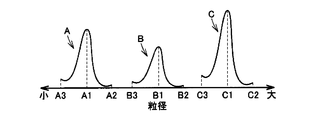
- the step of forming the second raw material in the step of forming the second raw material, there are a plurality of particle size distribution peaks in the range of 1 ⁇ m or more and 3 mm or less, and within a range of ⁇ 50% from the center of each particle size distribution peak.
- the second raw material is formed so that 95% or more of the particles are present.
- the present inventor has focused on the particle size of the second raw material and completed the above invention.
- the particle size distribution of the second raw material as described above, the filling rate of the second raw material into the crucible can be improved.
- the second SiC crystal can be manufactured at a reduced cost.
- the influence on the sublimation gas concentration of the second raw material can be reduced, the micropipe density, etch pit density, etc. of the second SiC crystal grown using the second raw material can be effectively reduced. . Therefore, the deterioration of the quality of the growing SiC crystal can be further reduced.
- the second raw material in the step of forming the second raw material, the second raw material having an Fe concentration of 0.1 ppm or less and an Al concentration of 100 ppm or less is formed.
- the step of forming the second raw material includes a step of washing the pulverized first SiC crystal with an acidic solution.
- the second SiC crystal is pulverized to form a third raw material, and the third raw material is heated to be sublimated to precipitate the SiC crystal. And a step of growing a third SiC crystal.
- the present inventor has found that the impurity concentration of the growing SiC crystal can be reduced by growing the SiC crystal using a crushed crystal as a raw material. For this reason, the impurity concentration of the growing SiC crystal can be gradually reduced by repeating the process of growing the SiC crystal using the pulverized SiC crystal as a raw material. For this reason, it is possible to further suppress the deterioration of the quality of the SiC crystal to be manufactured by repeating the step of growing the SiC crystal three times or more using the pulverized grown crystal as a raw material.
- the SiC crystal and the manufacturing method of the SiC crystal of the present invention it is possible to suppress deterioration of quality due to impurities.
- FIG. 1 is a perspective view schematically showing SiC crystal 10 in an embodiment of the present invention. First, SiC crystal 10 according to an embodiment of the present invention will be described with reference to FIG.
- the SiC crystal 10 is a substrate having a circular planar shape, for example.
- the SiC crystal 10 has Fe at a concentration of 0.1 ppm or less and Al at a concentration of 100 ppm or less.
- the Fe and Al concentrations are preferably as low as possible, but from the standpoint of easy realization, the Fe concentration is, for example, 0.002 ppm or more, and the Al concentration is, for example, 0.02 ppm.
- the concentrations of Fe and Al are values measured by, for example, ICP-AES.
- the micropipe density of SiC crystal 10 is preferably 10 pieces / cm 2 or less, and more preferably 2 pieces / cm 2 or less.
- the micropipe density is a value obtained from, for example, the number of penetrating hollow defects that were immersed in a potassium hydroxide (KOH) melt at 500 ° C. for 1 to 10 minutes and counted on the etched surface using a Nomarski differential interference microscope. .
- the etch pit density of SiC crystal 10 is preferably 10000 / cm 2 or less, and more preferably 9300 / cm 2 or less.
- the etch pit density is a value obtained from, for example, the number of etch pits counted using a Nomarski differential interference microscope for an etched surface immersed in a KOH melt at 500 ° C. for 1 to 10 minutes.
- the SiC crystal 10 is preferably a single crystal.
- the polytype of SiC crystal 10 is not particularly limited, but is preferably 4H—SiC, for example.
- SiC crystal 10 is manufactured by a sublimation method.
- 2, 3, 5, and 6 are cross-sectional views schematically showing a process for manufacturing the SiC crystal in the present embodiment.
- FIG. 4 is a diagram for explaining the particle size distribution of the second raw material in the present embodiment.
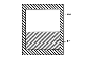
- the manufacturing apparatus includes a crucible 101 and a heating unit (not shown) for heating the crucible 101.
- a heating part is arrange
- the crucible 101 has a lower part that holds the raw material and an upper part that functions as a lower lid that holds the raw material.
- the crucible 101 is made of, for example, graphite.
- the manufacturing apparatus may include various elements other than those described above, but illustration and description of these elements are omitted for convenience of description.
- polishing SiC powder is prepared as the first raw material 17.
- GC polishing SiC powder
- the prepared first raw material 17 is installed in the lower part of the crucible 101.
- the first raw material 17 is sublimated by heating, and is precipitated from the gas of the first raw material 17 to grow the first SiC crystal 11.
- the first raw material 17 is heated by the heating unit at a temperature at which the first raw material 17 sublimes.
- the first raw material 17 is sublimated to generate a sublimation gas.
- the sublimation gas is solidified again at a position facing the first raw material inside the crucible 101, which is installed at a lower temperature than the first raw material 17, that is, at the upper part of the crucible 101.
- the temperature of the first raw material 17 is maintained at 2000 ° C. to 3000 ° C.
- the temperature at the position facing the first raw material 17 is 1900 ° C. to 2200 ° C.
- the first The temperature is kept lower than the temperature of the raw material 17.
- the atmospheric pressure inside the crucible 101 is preferably maintained at 400 Torr or less.
- first SiC crystal 11 grows at a position facing first raw material 17.
- First SiC crystal 11 grown in this way is, for example, polycrystalline.
- the growth rate of the 1st SiC crystal 11 can be raised.
- the temperature of the 1st raw material 17 shall be 3000 degrees C or less, damage to the crucible 101 can be suppressed.
- the growth temperature may be maintained at a constant temperature during growth or may be changed at a certain rate during growth.
- the growth rate can be increased.
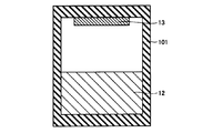
- the first SiC crystal 11 is pulverized to form the second raw material 12 (see FIG. 5).
- This step is performed as follows, for example. Specifically, the inside of the crucible 101 is cooled to room temperature. Then, the first SiC crystal 11 grown from the crucible 101 is taken out. The first SiC crystal 11 is pulverized using, for example, a pulverizer. The method for pulverizing is not particularly limited.
- this step there are a plurality of particle size distribution peaks (three peaks A, B, and C in FIG. 4) in the range of 1 ⁇ m to 3 mm, and each of the particle size distribution peaks A, B, It is preferable to form the second raw material 12 so that 95% or more of the particles exist in a range of ⁇ 50% from the C centers A1, B1, and C1.
- the center A1, B1, C1 of the peak A, B, C of the particle size distribution is 1 ⁇ m or more and 3 ⁇ m or less, and within the range of ⁇ 50% from the center A1, B1, C1 of each peak A, B, C of the particle size distribution
- the presence of 95% or more of the particles can increase the filling rate when the crucible 101 is filled with the second raw material 12. Thereby, the growth time when growing the second SiC crystal 14 using the second raw material 12 is shortened, and it is possible to suppress the influence of the gas concentration of the second raw material 12 sublimated during the growth. For this reason, the quality of the 2nd SiC crystal 14 grown using this 2nd raw material 12 can be raised.
- the second raw material 12 is formed so that the center A1 of the peak A with the minimum particle size is 1 ⁇ m or more and 100 ⁇ m or less and the center C1 of the peak C with the maximum particle size is 200 ⁇ m or more and 3 mm or less. Is preferred.
- the peak A includes particles of 10 wt% or more and 50 wt% or less
- the peak C includes particles of 30 wt% or more and 80 wt% or less
- the remainder is the other peak (peak B in FIG. 4). More preferably, the second raw material 12 is formed.
- “there is 95% or more of particles in the range of ⁇ 50% from the centers A1, B1, and C1 of the peaks A, B, and C of each particle size distribution” means that the particles of the centers A1, B1, and C1 exist. Between the particle diameters A2, B2, C2 of 150% with respect to the diameter and the particle diameters A3, B3, C3 of 50% with respect to the particle diameters of the centers A1, B1, C1, the entire particles of the second raw material 12 It means that 95% or more exists.
- the number of peaks in the particle size distribution may be two or four or more.
- particle size distribution is a value measured in accordance with, for example, JIS R6001 1998.
- the method of forming the second raw material 12 having the particle size distribution as described above is not particularly limited.
- 2 raw materials 12 can be formed.
- the first SiC crystal 11 is pulverized, it is preferable to wash the pulverized first SiC crystal 11 with an acidic solution.
- the acidic solution is not particularly limited, but it is preferable to use aqua regia.
- an acidic solution, particularly aqua regia heavy metals such as Fe adhering to the first SiC crystal 11 can be removed during pulverization.
- the second raw material 12 formed as described above contains Fe having a concentration of 0.1 ppm or less and Al having a concentration of 100 ppm or less.
- the second raw material 12 formed as described above is placed under the crucible 101.
- a seed substrate 13 is disposed on the crucible 101 so as to face the second raw material 12 in the crucible 101.
- the main surface of the seed substrate 13 may be circular or quadrangular.
- the material of the seed substrate 13 is not particularly limited, but is preferably a SiC substrate from the viewpoint of improving the quality of the growing second SiC crystal 14, and is the same as the growing polytype (crystal polymorph). Is more preferable. For example, when the SiC crystal intended to grow is 4H—SiC, it means that the seed substrate 13 is also 4H—SiC. Note that this step may be omitted.
- the second raw material 12 is sublimated by heating and precipitated from the gas of the second raw material 12 to grow the second SiC crystal 14.
- second SiC crystal 14 is grown on seed substrate 13.
- Second SiC crystal 14 is preferably a single crystal. Since the growth method of second SiC crystal 14 is substantially the same as the growth method of first SiC crystal 11, the description thereof will not be repeated.
- the inside of the crucible 101 is cooled to room temperature.
- the ingot provided with the seed substrate 13 and the 2nd SiC crystal 14 is taken out from the crucible 101.
- This ingot may be the SiC crystal 10 shown in FIG. That is, the first SiC crystal 11 is grown using the first raw material 17, the first SiC crystal 11 is pulverized to form the second raw material 12, and the second raw material 12 is used to form the second raw material 12.
- the SiC crystal 10 of FIG. 1 may be manufactured by growing the SiC crystal 14.
- the second SiC crystal 14 is pulverized to form a third raw material, and the third raw material is sublimated by heating and precipitated from the gas of the third raw material. It is preferable to further perform the step of growing the SiC crystal. By this one cycle process, for example, about 10% of impurities can be reduced.
- the impurity concentration of the grown SiC crystal 10 is reduced.
- the concentration of Fe in the grown SiC crystal is 0.1 ppm or less. It is preferable to repeat the above steps until the concentration of Al becomes 100 ppm or less. In order to reliably produce such a SiC crystal, the above steps are repeated until a raw material having an Fe concentration of 0.1 ppm or less and an Al concentration of 100 ppm or less can be produced. It is more preferable to produce a SiC crystal by growing.
- an ingot including a seed substrate and a SiC crystal formed on the seed substrate can be manufactured.
- This ingot may be the SiC crystal 10 shown in FIG.
- the SiC crystal 10 shown in FIG. 1 may be manufactured by removing the seed substrate 13 from the ingot. When removing, only the seed substrate 13 may be removed, or the seed substrate 13 and a part of the grown SiC crystal may be removed.
- the removal method is not particularly limited, and a mechanical removal method such as cutting, grinding, and cleavage can be used.
- Cutting means that at least the seed substrate 13 is mechanically removed from the ingot with, for example, a wire saw. Grinding refers to scraping in the thickness direction by contacting the surface while rotating the grindstone.
- Cleaving means dividing the crystal along the crystal lattice plane. A chemical removal method such as etching may be used.
- the SiC crystal 10 shown in FIG. 1 may be manufactured by cutting a plurality of SiC crystals from the grown SiC crystal. In this case, the manufacturing cost of one SiC crystal 10 can be reduced.
- one or both surfaces of the SiC crystal may be planarized by grinding, polishing, or the like.
- the method for manufacturing SiC crystal 10 includes a step of preparing a SiC powder for polishing as first raw material 17 and sublimating by heating first raw material 17.
- the step of growing the first SiC crystal 11 by precipitating the SiC crystal, the step of crushing the first SiC crystal 11 to form the second raw material 12, and the second raw material 12 A step of growing the second SiC crystal 14 by sublimating by heating to precipitate a crystal of SiC.
- the inventor pulverizes the first SiC crystal 11 grown using the first raw material 17 to produce the second raw material 12, and grows the second SiC crystal 14 using the second raw material 12. Then, the knowledge that the second SiC crystal 14 can reduce impurities such as Fe and Al as compared with the first SiC crystal 11 has been obtained.
- first SiC crystal 11 is grown using a GC raw material as first raw material 17, and the first SiC crystal 11 is pulverized to produce the second A raw material 12 is formed, and a second SiC crystal 14 is grown using the second raw material 12.
- the second SiC crystal 14 can have a lower impurity concentration than the first SiC crystal 11. Therefore, it can reduce that quality deteriorates due to impurities about SiC crystal 10 to be manufactured.
- the SiC crystal 10 can be manufactured at a reduced cost.
- SiC crystal 10 having an Fe concentration of 0.1 ppm or less and an Al concentration of 100 ppm or less can be manufactured.
- the inventor has intensively studied to what extent the impurity concentration of Fe and Al in the SiC crystal 10 can be reduced to reduce the influence on the quality caused by the impurities.
- the influence on the quality of SiC crystal 10 for example, crystal defects such as micropipes and etch pits
- SiC crystal 10 of the present embodiment quality deterioration can be suppressed.
- the first SiC crystal 11 is grown using GC as the first raw material 17, the first SiC crystal 11 is pulverized to form the second raw material 12, and the second raw material 12 is The effect of growing the second SiC crystal 14 by using it was investigated.
- Example 1 of the present invention an SiC crystal was basically manufactured according to the SiC crystal manufacturing method in the above-described embodiment.
- first raw material 17 a commercially available GC for abrasives was prepared as the first raw material 17. As shown in FIG. 2, this first raw material was placed at the bottom of the crucible 101, and nothing was placed on the lid of the crucible 101 facing the outermost surface of the first raw material 17.
- the first raw material 17 was sublimated by heating, and the first SiC crystal 11 was grown by precipitating the gas of the first raw material 17.
- the temperature of the lower part of the crucible 101 that is, the temperature of the first raw material 17 was 2300 ° C.
- the upper part of the crucible 101 was 2000 ° C.
- the pressure inside the crucible 101 was 1 Torr.
- the grown first SiC crystal 11 was polycrystalline.
- the first SiC crystal 11 was pulverized.
- the pulverization was performed using a pulverizer. Thereafter, the ground first SiC crystal 11 was washed with aqua regia and further washed with hydrochloric acid. Then, using the pulverized first SiC crystal 11, as shown in FIG. 4, there are three peak A, B, C of the particle size distribution, the center of the peak A of the minimum particle size is less than 1 ⁇ m, and the maximum particle size
- the second raw material 12 was formed so that the center of the peak C exceeded 3 mm. Further, the second raw material 12 was formed so that 95% or more of the particles were present in the range of ⁇ 50% from the center of each particle size distribution peak.
- the particle size distribution of the second raw material 12 was measured in accordance with JIS R6001 1998. The second raw material 12 was placed in the lower part inside the crucible 101.
- 4H—SiC having a micropipe density of 10 pieces / cm 2 was prepared as a seed substrate 13.
- This seed substrate 13 was disposed so as to face the second raw material 12 in the upper part inside the crucible 101.
- the second raw material 12 was sublimated by heating, and the second SiC crystal 14 was grown by precipitating the gas of the second raw material 12.
- the growth method of the second SiC crystal 14 was the same as the growth method of the first SiC crystal 11.
- the SiC crystal of Example 1 of the present invention was produced. That is, the second SiC crystal 14 was used as the SiC crystal of Example 1 of the present invention.
- invention Example 2 The production method of the SiC crystal of Invention Example 2 was basically produced in the same manner as that of Invention Example 1, but in the step of forming the second raw material 12, the center of the peak C of the maximum particle size was 200 ⁇ m or more and 3 mm or less. In that the second raw material 12 was formed.
- the production method of the SiC crystal of Invention Example 3 was basically produced in the same manner as in Invention Example 1, but in the step of forming the second raw material 12, the center of the peak A of the minimum particle size was 1 ⁇ m or more and 100 ⁇ m or less. In that the second raw material 12 was formed.
- the SiC crystal production method of Inventive Example 4 was basically produced in the same manner as in Inventive Example 1, but in the step of forming the second raw material 12, the center of the peak A of the minimum particle size was 1 ⁇ m or more and 100 ⁇ m or less. And the center of the peak C of the maximum particle size was different in that the second raw material 12 having a diameter of 200 ⁇ m or more and 3 mm or less was formed.
- Comparative Example 1 The manufacturing method of the SiC crystal of Comparative Example 1 was basically manufactured in the same manner as Example 1 of the present invention, but the step of pulverizing the first SiC crystal 11 to form the second raw material was not performed. Was different. That is, the first SiC crystal 11 was the SiC crystal of Comparative Example 1.
- the concentrations of Al and Fe were measured by ICP (Inductive Coupled Plasma) -AES (Atomic Emission Spectrometry) (inductively coupled plasma atomic emission spectrometry).
- the detection limit of Al was 0.02 ppm, and the detection limit of Fe was 0.002 ppm.
- micropipe density was determined by slicing the SiC crystals of Invention Examples 1 to 4 and Comparative Example 1 so as to have a surface 10 mm away from the surface in contact with the seed substrate 13, and then KOH melt at 500 ° C. The number of penetrating hollow defects counted using a Nomarski differential interference microscope on the etched surface immersed for 1 to 10 minutes was determined. Further, the micropipe density of the SiC crystal grown on the seed substrate 13 (the MPD of the crystal / the MPD of the seed substrate in Table 1) was also calculated with respect to the micropipe density of the seed substrate 13.
- the etch pit density was determined by slicing the SiC crystals of Invention Examples 1 to 4 and Comparative Example 1 so as to have a surface 10 mm away from the surface in contact with the seed substrate 13, and then KOH melt at 500 ° C. It was determined from the number of etch pits counted using a Nomarski differential interference microscope for the etched surface immersed for 1-10 minutes.
- the first SiC crystal 11 is grown using the first raw material 17, the first SiC crystal 11 is pulverized to form the second raw material 12, and the second raw material 12 is Inventive Examples 1 to 4, in which the second SiC crystal 14 was grown using the same, were able to reduce the concentrations of Al and Fe as compared with Comparative Example 1. Moreover, it turned out that the SiC crystal containing 0.1 ppm or less of Fe and 100 ppm or less of Al can be implement
- the SiC crystals of Examples 1 to 4 of the present invention can reduce the micropipe density and the etch pit density as compared with the SiC crystal of Comparative Example 1. Further, it was also found that the SiC crystals of Examples 1 to 4 of the present invention were reduced in taking over the micropipe of the seed substrate 13 as compared with the SiC crystal of Comparative Example 1.
- the present invention example 4 in which the second raw material was formed can reduce the micropipe density and the etch pit density more than the present invention examples 1 to 3. Moreover, it turned out that taking over the micropipe of the seed substrate 13 is reduced more.
- the first SiC crystal 11 is grown using the first raw material 17, the first SiC crystal 11 is pulverized to form the second raw material 12, and the second It has been confirmed that by growing the second SiC crystal 14 using the raw material 12, impurities can be reduced and deterioration in quality can be suppressed.
Landscapes
- Chemical & Material Sciences (AREA)
- Engineering & Computer Science (AREA)
- Crystallography & Structural Chemistry (AREA)
- Materials Engineering (AREA)
- Metallurgy (AREA)
- Organic Chemistry (AREA)
- Inorganic Chemistry (AREA)
- Crystals, And After-Treatments Of Crystals (AREA)
- Physical Deposition Of Substances That Are Components Of Semiconductor Devices (AREA)
- Carbon And Carbon Compounds (AREA)
Priority Applications (7)
| Application Number | Priority Date | Filing Date | Title |
|---|---|---|---|
| CN2011800043891A CN102597339A (zh) | 2010-04-26 | 2011-02-25 | 碳化硅晶体和制造碳化硅晶体的方法 |
| KR1020127009040A KR20120130318A (ko) | 2010-04-26 | 2011-02-25 | 탄화규소 결정 및 탄화규소 결정의 제조 방법 |
| CA2775923A CA2775923A1 (en) | 2010-04-26 | 2011-02-25 | Silicon carbide crystal and method of manufacturing silicon carbide crystal |
| US13/499,482 US8574529B2 (en) | 2010-04-26 | 2011-02-25 | Silicon carbide crystal and method of manufacturing silicon carbide crystal |
| EP11774697.4A EP2565301B1 (en) | 2010-04-26 | 2011-02-25 | Silicon carbide crystal and method for producing silicon carbide crystal |
| US14/019,882 US20140004303A1 (en) | 2010-04-26 | 2013-09-06 | Silicon carbide crystal and method of manufacturing silicon carbide crystal |
| US15/185,602 US9725823B2 (en) | 2010-04-26 | 2016-06-17 | Silicon carbide crystal and method of manufacturing silicon carbide crystal |
Applications Claiming Priority (2)
| Application Number | Priority Date | Filing Date | Title |
|---|---|---|---|
| JP2010-100891 | 2010-04-26 | ||
| JP2010100891A JP5565070B2 (ja) | 2010-04-26 | 2010-04-26 | 炭化珪素結晶および炭化珪素結晶の製造方法 |
Related Child Applications (2)
| Application Number | Title | Priority Date | Filing Date |
|---|---|---|---|
| US13/499,482 A-371-Of-International US8574529B2 (en) | 2010-04-26 | 2011-02-25 | Silicon carbide crystal and method of manufacturing silicon carbide crystal |
| US14/019,882 Continuation US20140004303A1 (en) | 2010-04-26 | 2013-09-06 | Silicon carbide crystal and method of manufacturing silicon carbide crystal |
Publications (1)
| Publication Number | Publication Date |
|---|---|
| WO2011135913A1 true WO2011135913A1 (ja) | 2011-11-03 |
Family
ID=44861234
Family Applications (1)
| Application Number | Title | Priority Date | Filing Date |
|---|---|---|---|
| PCT/JP2011/054339 Ceased WO2011135913A1 (ja) | 2010-04-26 | 2011-02-25 | 炭化珪素結晶および炭化珪素結晶の製造方法 |
Country Status (8)
| Country | Link |
|---|---|
| US (3) | US8574529B2 (https=) |
| EP (1) | EP2565301B1 (https=) |
| JP (1) | JP5565070B2 (https=) |
| KR (1) | KR20120130318A (https=) |
| CN (1) | CN102597339A (https=) |
| CA (1) | CA2775923A1 (https=) |
| TW (1) | TW201142092A (https=) |
| WO (1) | WO2011135913A1 (https=) |
Families Citing this family (9)
| Publication number | Priority date | Publication date | Assignee | Title |
|---|---|---|---|---|
| JP5910393B2 (ja) | 2012-07-26 | 2016-04-27 | 住友電気工業株式会社 | 炭化珪素基板の製造方法 |
| JP6028754B2 (ja) | 2014-03-11 | 2016-11-16 | トヨタ自動車株式会社 | SiC単結晶基板の製造方法 |
| US10108798B1 (en) * | 2016-01-04 | 2018-10-23 | Smart Information Flow Technologies LLC | Methods and systems for defending against cyber-attacks |
| CN105603530B (zh) * | 2016-01-12 | 2018-02-27 | 台州市一能科技有限公司 | 用于碳化硅晶体高速生长的原料及碳化硅晶体的生长方法 |
| JP6086167B2 (ja) * | 2016-03-18 | 2017-03-01 | 住友電気工業株式会社 | 炭化珪素基板の製造方法 |
| WO2018176302A1 (zh) * | 2017-03-30 | 2018-10-04 | 新疆天科合达蓝光半导体有限公司 | 用于生长SiC晶体的SiC原料的制备方法和制备装置 |
| CN115704110A (zh) * | 2021-08-06 | 2023-02-17 | 株式会社电装 | 碳化硅晶体制造设备、其控制装置及生成学习模型和控制其的方法 |
| KR102442731B1 (ko) | 2021-12-23 | 2022-09-13 | 주식회사 쎄닉 | 탄화규소 분말 및 이를 이용하여 탄화규소 잉곳을 제조하는 방법 |
| KR102442730B1 (ko) * | 2021-12-23 | 2022-09-13 | 주식회사 쎄닉 | 탄화규소 분말, 이를 이용하여 탄화규소 잉곳을 제조하는 방법 및 탄화규소 웨이퍼 |
Citations (6)
| Publication number | Priority date | Publication date | Assignee | Title |
|---|---|---|---|---|
| JPS6350393A (ja) * | 1986-08-20 | 1988-03-03 | Sanyo Electric Co Ltd | SiC単結晶の成長方法 |
| JPH0948605A (ja) * | 1995-05-31 | 1997-02-18 | Bridgestone Corp | 炭化ケイ素単結晶製造用高純度炭化ケイ素粉体の製造方法及び単結晶 |
| JP2005008473A (ja) | 2003-06-18 | 2005-01-13 | Nippon Steel Corp | 高純度炭化珪素単結晶、単結晶ウェハおよびその製造方法 |
| JP2005239496A (ja) * | 2004-02-27 | 2005-09-08 | Nippon Steel Corp | 炭化珪素単結晶育成用炭化珪素原料と炭化珪素単結晶及びその製造方法 |
| JP2005314217A (ja) | 2004-03-29 | 2005-11-10 | Nippon Steel Corp | 炭化珪素単結晶およびその製造方法 |
| JP2010083681A (ja) * | 2008-09-29 | 2010-04-15 | Bridgestone Corp | 炭化ケイ素単結晶の製造方法及び真空チャック |
Family Cites Families (13)
| Publication number | Priority date | Publication date | Assignee | Title |
|---|---|---|---|---|
| JPS58147493A (ja) | 1982-02-12 | 1983-09-02 | フイリツプス・ペトロリユ−ム・コンパニ− | 熱分解法用の防汚剤 |
| JPS58187479A (ja) | 1982-04-27 | 1983-11-01 | Honda Motor Co Ltd | 可撓シ−ル材の外被材貼付方法 |
| JPH0645519B2 (ja) * | 1986-08-18 | 1994-06-15 | 三洋電機株式会社 | p型SiC単結晶の成長方法 |
| US5863325A (en) | 1995-05-31 | 1999-01-26 | Bridgestone Corporation | Process for producing high purity silicon carbide powder for preparation of a silicon carbide single crystal and single crystal |
| JP3590464B2 (ja) | 1995-12-08 | 2004-11-17 | 新日本製鐵株式会社 | 4h型単結晶炭化珪素の製造方法 |
| US7553373B2 (en) * | 2001-06-15 | 2009-06-30 | Bridgestone Corporation | Silicon carbide single crystal and production thereof |
| SE520968C2 (sv) * | 2001-10-29 | 2003-09-16 | Okmetic Oyj | Högresistiv monokristallin kiselkarbid och metod för dess framställning |
| JP4593099B2 (ja) * | 2003-03-10 | 2010-12-08 | 学校法人関西学院 | 単結晶炭化ケイ素の液相エピタキシャル成長法及びそれに用いられる熱処理装置 |
| US20060249073A1 (en) | 2003-03-10 | 2006-11-09 | The New Industry Research Organization | Method of heat treatment and heat treatment apparatus |
| WO2006017074A2 (en) * | 2004-07-07 | 2006-02-16 | Ii-Vi Incorporated | Low-doped semi-insulating sic crystals and method |
| JP2007284306A (ja) * | 2006-04-19 | 2007-11-01 | Nippon Steel Corp | 炭化珪素単結晶及びその製造方法 |
| CN101536168A (zh) * | 2006-09-14 | 2009-09-16 | 科锐有限公司 | 无微管碳化硅及其相关制备方法 |
| JP2010095397A (ja) * | 2008-10-15 | 2010-04-30 | Nippon Steel Corp | 炭化珪素単結晶及び炭化珪素単結晶ウェハ |
-
2010
- 2010-04-26 JP JP2010100891A patent/JP5565070B2/ja active Active
-
2011
- 2011-02-25 EP EP11774697.4A patent/EP2565301B1/en active Active
- 2011-02-25 CN CN2011800043891A patent/CN102597339A/zh active Pending
- 2011-02-25 WO PCT/JP2011/054339 patent/WO2011135913A1/ja not_active Ceased
- 2011-02-25 CA CA2775923A patent/CA2775923A1/en not_active Abandoned
- 2011-02-25 US US13/499,482 patent/US8574529B2/en active Active
- 2011-02-25 KR KR1020127009040A patent/KR20120130318A/ko not_active Ceased
- 2011-04-15 TW TW100113266A patent/TW201142092A/zh unknown
-
2013
- 2013-09-06 US US14/019,882 patent/US20140004303A1/en not_active Abandoned
-
2016
- 2016-06-17 US US15/185,602 patent/US9725823B2/en active Active
Patent Citations (6)
| Publication number | Priority date | Publication date | Assignee | Title |
|---|---|---|---|---|
| JPS6350393A (ja) * | 1986-08-20 | 1988-03-03 | Sanyo Electric Co Ltd | SiC単結晶の成長方法 |
| JPH0948605A (ja) * | 1995-05-31 | 1997-02-18 | Bridgestone Corp | 炭化ケイ素単結晶製造用高純度炭化ケイ素粉体の製造方法及び単結晶 |
| JP2005008473A (ja) | 2003-06-18 | 2005-01-13 | Nippon Steel Corp | 高純度炭化珪素単結晶、単結晶ウェハおよびその製造方法 |
| JP2005239496A (ja) * | 2004-02-27 | 2005-09-08 | Nippon Steel Corp | 炭化珪素単結晶育成用炭化珪素原料と炭化珪素単結晶及びその製造方法 |
| JP2005314217A (ja) | 2004-03-29 | 2005-11-10 | Nippon Steel Corp | 炭化珪素単結晶およびその製造方法 |
| JP2010083681A (ja) * | 2008-09-29 | 2010-04-15 | Bridgestone Corp | 炭化ケイ素単結晶の製造方法及び真空チャック |
Non-Patent Citations (1)
| Title |
|---|
| See also references of EP2565301A4 |
Also Published As
| Publication number | Publication date |
|---|---|
| US20120183466A1 (en) | 2012-07-19 |
| US20160289863A1 (en) | 2016-10-06 |
| US9725823B2 (en) | 2017-08-08 |
| EP2565301A4 (en) | 2013-11-27 |
| EP2565301A1 (en) | 2013-03-06 |
| TW201142092A (en) | 2011-12-01 |
| CA2775923A1 (en) | 2011-11-03 |
| CN102597339A (zh) | 2012-07-18 |
| KR20120130318A (ko) | 2012-11-30 |
| JP2011230941A (ja) | 2011-11-17 |
| US20140004303A1 (en) | 2014-01-02 |
| JP5565070B2 (ja) | 2014-08-06 |
| EP2565301B1 (en) | 2015-03-25 |
| US8574529B2 (en) | 2013-11-05 |
Similar Documents
| Publication | Publication Date | Title |
|---|---|---|
| JP5565070B2 (ja) | 炭化珪素結晶および炭化珪素結晶の製造方法 | |
| JP6537590B2 (ja) | 炭化珪素単結晶インゴットの製造方法 | |
| JP6742183B2 (ja) | 炭化珪素単結晶インゴットの製造方法 | |
| JP7747730B2 (ja) | 高品質の炭化ケイ素種結晶、炭化ケイ素結晶、炭化ケイ素基板およびそれらの製造方法 | |
| KR20130137247A (ko) | 탄화규소 단결정 기판 및 그 제조 방법 | |
| JP6624868B2 (ja) | p型低抵抗率炭化珪素単結晶基板 | |
| JP5402701B2 (ja) | 炭化珪素結晶の製造方法 | |
| JP2017065986A (ja) | 低抵抗率炭化珪素単結晶基板の製造方法 | |
| CN106103815A (zh) | SiC单晶的制造方法 | |
| JP2012250897A (ja) | 単結晶炭化珪素基板およびその製造方法 | |
| JP7481763B2 (ja) | 炭化珪素ウエハ及びその製造方法 | |
| KR102218607B1 (ko) | 탄화규소의 분말의 제조 방법 | |
| JP2015012124A (ja) | 半導体ウェハのエッチング方法、半導体ウェハとその製造方法および半導体ウェハの結晶欠陥検出方法。 | |
| JP5135545B2 (ja) | 炭化珪素単結晶インゴット育成用種結晶及びその製造方法 | |
| JP6304477B2 (ja) | 炭化珪素粉粒体及びその製造方法 | |
| JP2022155538A (ja) | 炭化珪素ウエハ及びこれを適用した半導体素子 | |
| JP2022062043A (ja) | ウエハの製造方法、エピタキシャルウエハの製造方法、これによって製造されたウエハ及びエピタキシャルウエハ | |
| JP6695182B2 (ja) | 炭化珪素単結晶成長用種結晶の製造方法及び炭化珪素単結晶インゴットの製造方法 | |
| US20240059570A1 (en) | Silicon carbide powder, method for manufacturing the same and method for manufacturing silicon carbide ingot using the same | |
| KR102236397B1 (ko) | 탄화규소 웨이퍼 및 이를 적용한 반도체 소자 | |
| US12359344B2 (en) | Silicon carbide powder and method for manufacturing silicon carbide ingot using the same | |
| KR102567936B1 (ko) | 탄화규소 분말, 이의 제조방법 및 이를 이용하여 탄화규소 잉곳을 제조하는 방법 | |
| JP2015030659A (ja) | 単結晶の製造方法 | |
| JP2014015394A (ja) | 炭化珪素結晶の製造方法 |
Legal Events
| Date | Code | Title | Description |
|---|---|---|---|
| WWE | Wipo information: entry into national phase |
Ref document number: 201180004389.1 Country of ref document: CN |
|
| 121 | Ep: the epo has been informed by wipo that ep was designated in this application |
Ref document number: 11774697 Country of ref document: EP Kind code of ref document: A1 |
|
| WWE | Wipo information: entry into national phase |
Ref document number: 2011774697 Country of ref document: EP |
|
| WWE | Wipo information: entry into national phase |
Ref document number: 2775923 Country of ref document: CA |
|
| WWE | Wipo information: entry into national phase |
Ref document number: 13499482 Country of ref document: US |
|
| ENP | Entry into the national phase |
Ref document number: 20127009040 Country of ref document: KR Kind code of ref document: A |
|
| NENP | Non-entry into the national phase |
Ref country code: DE |