EP2552008A1 - Umrichtervorrichtung und elektrische vorrichtung damit - Google Patents
Umrichtervorrichtung und elektrische vorrichtung damit Download PDFInfo
- Publication number
- EP2552008A1 EP2552008A1 EP10848326A EP10848326A EP2552008A1 EP 2552008 A1 EP2552008 A1 EP 2552008A1 EP 10848326 A EP10848326 A EP 10848326A EP 10848326 A EP10848326 A EP 10848326A EP 2552008 A1 EP2552008 A1 EP 2552008A1
- Authority
- EP
- European Patent Office
- Prior art keywords
- circuit
- switching circuit
- arm switching
- inverter device
- driven
- Prior art date
- Legal status (The legal status is an assumption and is not a legal conclusion. Google has not performed a legal analysis and makes no representation as to the accuracy of the status listed.)
- Withdrawn
Links
- 239000003990 capacitor Substances 0.000 claims description 39
- 238000000034 method Methods 0.000 claims description 32
- 239000004065 semiconductor Substances 0.000 claims description 9
- JMASRVWKEDWRBT-UHFFFAOYSA-N Gallium nitride Chemical group [Ga]#N JMASRVWKEDWRBT-UHFFFAOYSA-N 0.000 claims description 5
- 238000010586 diagram Methods 0.000 description 16
- 238000009499 grossing Methods 0.000 description 7
- 230000016507 interphase Effects 0.000 description 2
- 238000004904 shortening Methods 0.000 description 2
- 238000011144 upstream manufacturing Methods 0.000 description 2
- 229910002601 GaN Inorganic materials 0.000 description 1
- 239000000428 dust Substances 0.000 description 1
- 230000000694 effects Effects 0.000 description 1
- 238000010248 power generation Methods 0.000 description 1
- 238000005406 washing Methods 0.000 description 1
Images





Classifications
-
- H—ELECTRICITY
- H02—GENERATION; CONVERSION OR DISTRIBUTION OF ELECTRIC POWER
- H02M—APPARATUS FOR CONVERSION BETWEEN AC AND AC, BETWEEN AC AND DC, OR BETWEEN DC AND DC, AND FOR USE WITH MAINS OR SIMILAR POWER SUPPLY SYSTEMS; CONVERSION OF DC OR AC INPUT POWER INTO SURGE OUTPUT POWER; CONTROL OR REGULATION THEREOF
- H02M7/00—Conversion of AC power input into DC power output; Conversion of DC power input into AC power output
- H02M7/42—Conversion of DC power input into AC power output without possibility of reversal
- H02M7/44—Conversion of DC power input into AC power output without possibility of reversal by static converters
- H02M7/48—Conversion of DC power input into AC power output without possibility of reversal by static converters using discharge tubes with control electrode or semiconductor devices with control electrode
- H02M7/53—Conversion of DC power input into AC power output without possibility of reversal by static converters using discharge tubes with control electrode or semiconductor devices with control electrode using devices of a triode or transistor type requiring continuous application of a control signal
- H02M7/537—Conversion of DC power input into AC power output without possibility of reversal by static converters using discharge tubes with control electrode or semiconductor devices with control electrode using devices of a triode or transistor type requiring continuous application of a control signal using semiconductor devices only, e.g. single switched pulse inverters
- H02M7/5387—Conversion of DC power input into AC power output without possibility of reversal by static converters using discharge tubes with control electrode or semiconductor devices with control electrode using devices of a triode or transistor type requiring continuous application of a control signal using semiconductor devices only, e.g. single switched pulse inverters in a bridge configuration
- H02M7/5388—Conversion of DC power input into AC power output without possibility of reversal by static converters using discharge tubes with control electrode or semiconductor devices with control electrode using devices of a triode or transistor type requiring continuous application of a control signal using semiconductor devices only, e.g. single switched pulse inverters in a bridge configuration with asymmetrical configuration of switches
-
- H—ELECTRICITY
- H02—GENERATION; CONVERSION OR DISTRIBUTION OF ELECTRIC POWER
- H02M—APPARATUS FOR CONVERSION BETWEEN AC AND AC, BETWEEN AC AND DC, OR BETWEEN DC AND DC, AND FOR USE WITH MAINS OR SIMILAR POWER SUPPLY SYSTEMS; CONVERSION OF DC OR AC INPUT POWER INTO SURGE OUTPUT POWER; CONTROL OR REGULATION THEREOF
- H02M1/00—Details of apparatus for conversion
- H02M1/0048—Circuits or arrangements for reducing losses
- H02M1/0054—Transistor switching losses
-
- H—ELECTRICITY
- H02—GENERATION; CONVERSION OR DISTRIBUTION OF ELECTRIC POWER
- H02M—APPARATUS FOR CONVERSION BETWEEN AC AND AC, BETWEEN AC AND DC, OR BETWEEN DC AND DC, AND FOR USE WITH MAINS OR SIMILAR POWER SUPPLY SYSTEMS; CONVERSION OF DC OR AC INPUT POWER INTO SURGE OUTPUT POWER; CONTROL OR REGULATION THEREOF
- H02M1/00—Details of apparatus for conversion
- H02M1/08—Circuits specially adapted for the generation of control voltages for semiconductor devices incorporated in static converters
- H02M1/084—Circuits specially adapted for the generation of control voltages for semiconductor devices incorporated in static converters using a control circuit common to several phases of a multi-phase system
-
- H—ELECTRICITY
- H02—GENERATION; CONVERSION OR DISTRIBUTION OF ELECTRIC POWER
- H02P—CONTROL OR REGULATION OF ELECTRIC MOTORS, ELECTRIC GENERATORS OR DYNAMO-ELECTRIC CONVERTERS; CONTROLLING TRANSFORMERS, REACTORS OR CHOKE COILS
- H02P27/00—Arrangements or methods for the control of AC motors characterised by the kind of supply voltage
- H02P27/04—Arrangements or methods for the control of AC motors characterised by the kind of supply voltage using variable-frequency supply voltage, e.g. inverter or converter supply voltage
- H02P27/06—Arrangements or methods for the control of AC motors characterised by the kind of supply voltage using variable-frequency supply voltage, e.g. inverter or converter supply voltage using DC to AC converters or inverters
- H02P27/08—Arrangements or methods for the control of AC motors characterised by the kind of supply voltage using variable-frequency supply voltage, e.g. inverter or converter supply voltage using DC to AC converters or inverters with pulse width modulation
- H02P27/085—Arrangements or methods for the control of AC motors characterised by the kind of supply voltage using variable-frequency supply voltage, e.g. inverter or converter supply voltage using DC to AC converters or inverters with pulse width modulation wherein the PWM mode is adapted on the running conditions of the motor, e.g. the switching frequency
-
- Y—GENERAL TAGGING OF NEW TECHNOLOGICAL DEVELOPMENTS; GENERAL TAGGING OF CROSS-SECTIONAL TECHNOLOGIES SPANNING OVER SEVERAL SECTIONS OF THE IPC; TECHNICAL SUBJECTS COVERED BY FORMER USPC CROSS-REFERENCE ART COLLECTIONS [XRACs] AND DIGESTS
- Y02—TECHNOLOGIES OR APPLICATIONS FOR MITIGATION OR ADAPTATION AGAINST CLIMATE CHANGE
- Y02B—CLIMATE CHANGE MITIGATION TECHNOLOGIES RELATED TO BUILDINGS, e.g. HOUSING, HOUSE APPLIANCES OR RELATED END-USER APPLICATIONS
- Y02B70/00—Technologies for an efficient end-user side electric power management and consumption
- Y02B70/10—Technologies improving the efficiency by using switched-mode power supplies [SMPS], i.e. efficient power electronics conversion e.g. power factor correction or reduction of losses in power supplies or efficient standby modes
Definitions
- the present invention relates to an inverter device which includes a plurality of switching elements and drives a load such as a motor, and an electric apparatus using the same, and particularly to a vacuum cleaner using the inverter device for a driving device of a fan motor.
- An inverter device converts input power from a power supply into AC of a desired output frequency, which is used to drive a motor or the like.
- the inverter device generally includes a switching circuit which has a plurality of serial circuits where two switching elements on the upstream side and the downstream side according to an application direction of the power supply voltage are connected in series to each other.
- the switching circuit forming the upstream side is referred to as an "upper arm switching circuit”
- the switching circuit forming the downstream side is referred to as a "lower arm switching circuit”.
- As the switching element a voltage-driven IGBT (Insulated Gate Bipolar Transistor), a MOSFET, or the like is used.
- an inverter device in which the IGBT is used for the upper arm switching circuit, and the MOSFET is used for the lower arm switching circuit (for example, refer to PTL 1).
- This uses a characteristic where loss is small at the time of high voltage and high current output since a voltage between both ends is constant when the IGBT is turned on, and a high frequency switching characteristic due to the high turning-on and turning-off speed of the MOSFET and a characteristic where loss is small at the time of low voltage and low current output. Thereby, it is possible to improve efficiency of the inverter device.
- the upper arm switching circuit and the lower arm switching circuit are constituted by different kinds (the IGBT and the MOSFET) of voltage-driven switching elements, it is difficult to maximize efficiency of the inverter device in consideration of both of conduction loss and switching loss of the different switching elements.
- a power generation apparatus including an inverter circuit which has a bootstrap circuit using charge accumulated in a capacitor as a driving power supply of switching elements of the upper arm switching circuit and the lower arm switching circuit (for example, refer to PTL 2).
- the same element (IGBT) which is of a voltage-driven type is used for the switching elements of the upper arm switching circuit and the lower arm switching circuit.
- the upper arm switching circuit is driven by a PWM signal of a duty cycle which is equal to or less than a predetermined value.
- the present invention relates to an inverter device including an upper arm switching circuit, a lower arm switching circuit, a control unit driving them, voltage-driven switching elements of the upper arm switching circuit, current-driven switching elements of the lower arm switching circuit, and a bootstrap circuit applying a driving voltage to each switching element.
- An electric apparatus of the present invention has a configuration where the inverter device is used for a driving device of a motor. Thereby, it is possible to implement an electric apparatus having good driving efficiency at low cost.
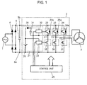
- Fig. 1 is a configuration diagram illustrating a configuration of an inverter device according to a first embodiment.
- AC power input from AC power supply 1 is temporarily converted into a DC power supply voltage by rectifying circuit 4 and smoothing capacitor 5 so as to be applied to inverter device 2, and three-phase (a U phase, a V phase, and a W phase) signals output from inverter device 2 are applied to by control unit 28 and drive motor 3.
- inverter device 2 is constituted by an upper arm switching circuit including switching elements 22, 23 and 24, a lower arm switching circuit including switching elements 25, 26 and 27, driving circuit 21 including bootstrap circuits, and control unit 28 controlling them. Respective corresponding pairs (22 and 25), (23 and 26) and (24 and 27) of the switching elements of the upper arm switching circuit and the lower arm switching circuit are connected in series and form three-phase serial circuits. In Fig. 1 , only the bootstrap circuit driving switching elements 22 and 25 is shown, and the bootstrap circuits driving switching elements 23 and 26 and switching elements 24 and 27 are not shown.
- switching elements 22, 23 and 24 of the upper arm switching circuit use, for example, a voltage-driven switching element such as an IGBT semiconductor device, and the switching elements are respective connected in parallel to free wheeling diodes 22a, 23a and 24a.
- Switching elements 25, 26 and 27 of the lower arm switching circuit use, for example, a current-driven gallium nitride (GaN) semiconductor device which can perform a switching operation at higher speed than switching elements 22, 23 and 24 of the upper arm switching circuit and has high efficiency.
- the voltage-driven switching element changes conduction due to a change in a voltage applied to the gate terminal
- the current-driven switching element changes conduction due to a change in a current applied to the gate terminal.
- connection points C1, C2 and C3 between the upper arm switching circuit and the lower arm switching circuit in the serial circuits are connected to motor 3 which is a load, and three-phase AC power is supplied thereto at a predetermined output frequency.
- Control unit 28 controls the respective switching elements 22 to 27 such that motor 3 rotates at a desired rotation rate, for example, inverter device 2 outputs three-phase AC power.
- a pulse width modulation hereinafter, referred to as a "PWM"
- PWM pulse width modulation
- the switching elements having different characteristics such as the voltage-driven type and the current-voltage type are used for the upper arm switching circuit and the lower arm switching circuit, which are driven by an optimal driving method in consideration of characteristics of the switching elements described below, and thereby it is possible to implement an inverter device having high efficiency with a low cost configuration.
- Driving circuit 21 is constituted by a bootstrap circuit which includes upper arm driver circuit 32, lower arm driver circuit 33, driver power supply 29, capacitor 31 of which the low voltage side is connected to connection point C1 between the upper arm switching circuit and the lower arm switching circuit, diode 30 connected between capacitor 31 and driver power supply 29.
- Driving circuit 21 drives the respective switching element pairs of the upper arm switching circuit and the lower arm switching circuit forming the respective phases.
- upper arm driver circuit 32 drives switching elements 22, 23 and 24 of the upper arm switching circuit
- the lower arm driver circuit 33 drives switching elements 25, 26 and 27 of the lower arm switching circuit.
- a driving voltage which is modulated into the carrier frequency of control unit 28 is supplied to the switching elements of the lower arm switching circuit from driver power supply 29 via lower arm driver circuit 33.
- a driving voltage which is modulated into the carrier frequency of control unit 28 is supplied to the switching elements of the upper arm switching circuit from capacitor 31 via upper arm driver circuit 32.
- both the upper arm switching circuit and the lower arm switching circuit can be driven by single driver power supply 29. For this reason, it is possible to implement a small-sized and low cost driving circuit.
- driving circuit 21 constituted by a bootstrap circuit can use only very low power for driving in order to supply a driving voltage for driving upper arm driver circuit 32 with charge accumulated in capacitor 31. Therefore, if a voltage-driven switching element which can be driven with very low power is used for the upper arm switching circuit, it is possible to perform driving with charge accumulated in capacitor 31. On the other hand, if a current-driven switching element which requires high power is used for the upper arm switching circuit, a capacitor having very large capacitance is required for driving, and thus costs of a driving circuit is increased and the driving circuit becomes large-sized.
- voltage-driven switching elements 22, 23 and 24 such as, for example, an IGBT semiconductor device are used for the upper arm switching circuit, and thereby it is possible to realize driving of the switching elements using the bootstrap circuit having small-sized and small capacitance capacitor 31.
- current-driven switching elements 25, 26 and 27 such as, for example, a GaN semiconductor device, are used for the lower arm switching circuit. At this time, the lower arm switching circuit can be directly driven by the driver power supply 29, and thus current-driven switching elements 25, 26 and 27 can be easily driven even though driving circuit 21 is constituted by the bootstrap circuit.
- circuit loss with respect to the carrier frequency of the inverter device will be described with reference to the drawings.
- the circuit loss includes conduction loss of the switching elements and switching loss.
- Fig. 2 is a schematic diagram illustrating circuit loss with respect to the carrier frequency of the inverter device according to the first embodiment of the present invention.
- circuit loss generated in the switching elements is increased as the carrier frequency of the PWM is heightened.
- the circuit loss of the switching elements is not varied with respect to the carrier frequency.
- the circuit loss of the voltage-driven switching elements used for the upper arm switching circuit is larger than the circuit loss of the current-driven switching elements used for the lower arm switching circuit.
- an increase rate of the circuit loss with respect to the carrier frequency when the PWM driving is performed is smaller in the switching elements of the lower arm switching circuit.
- the circuit loss in a case where the PWM driving is not performed is also smaller in the switching elements of the lower arm switching circuit.
- gallium nitride (GaN) semiconductor device used for switching elements 25, 26 and 27 of the lower arm switching circuit has smaller conduction (turned-on) loss than the IGBT semiconductor device used for switching elements 22, 23 and 24 of the upper arm switching circuit, can perform a high-speed switching operation, and thus efficiency is high.
- GaN gallium nitride
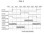
- Fig. 3 is a diagram illustrating a driving method in a case where only the lower arm switching circuit is PWM-driven in the inverter device according to the first embodiment of the present invention.
- Fig. 4 is a diagram illustrating a driving method in a case where only the upper arm switching circuit is PWM-driven in the inverter device according to the first embodiment of the present invention.
- an output voltage is adjusted by changing voltages applied in three phases (the U phase, the V phase, and the W phase) every 120 degrees with respect to phase angles of a rotor of the motor and changing conduction ratios (duty) of the switching elements of the lower arm switching circuit which is PWM-driven.
- an output voltage is adjusted by changing voltages applied in three phases (the U phase, the V phase, and the W phase) every 120 degrees with respect to phase angles of the rotor of the motor and changing conduction ratios (duty) of the switching elements of the upper arm switching circuit which is PWM-driven.
- the circuit loss in the driving methods shown in Figs. 3 and 4 is a sum of the respective circuit losses as shown in Fig. 2 .
- the circuit loss is a sum of the circuit loss of the switching elements of the lower arm switching circuit when the PWM driving is performed and the circuit loss of the switching elements of the upper arm switching circuit when the PWM driving is not performed.
- the circuit loss is a sum of the circuit loss of the switching elements of the upper arm switching circuit when the PWM driving is performed and the circuit loss of the switching elements of the lower arm switching circuit when the PWM driving is not performed.
- the circuit loss is lower in a case where only the lower arm switching circuit is PWM-driven.
- the carrier frequency is smaller (lower) than predetermined carrier frequency f1
- the circuit loss is lower in a case where only the upper arm switching circuit is PWM-driven.
- the inverter device of the present invention uses the switching elements of different characteristics (voltage-driven and current-driven types) for the upper arm switching circuit and the lower arm switching circuit, and can optimally perform driving with a low circuit loss so as to be suitable for the characteristics of the respective switching elements by changing the PWM driving at predetermined carrier frequency f1.
- the PWM driving at predetermined carrier frequency f1.
- Fig. 5 is a diagram illustrating an output frequency for changing the PWM driving of the inverter device according to the first embodiment of the present invention.
- Fig. 5 shows a case where the carrier frequency is greater (higher) than predetermined carrier frequency f1 as an example.
- Fig. 5 shows a case where only the upper arm switching circuit shown in Fig. 4 is PWM-driven when an AC output frequency output by the inverter device is equal to or less than predetermined output frequency s1.
- predetermined output frequency s1 is an output frequency where a voltage of the capacitor of the bootstrap circuit is the same as a driving voltage for driving the switching elements of the upper arm switching circuit via the upper arm driver circuit.
- the bootstrap circuit forming driving circuit 21 of the inverter device of the present embodiment accumulates charge in capacitor 31 for a time when the lower arm switching circuit is conducted (turned on), and drives the switching elements of the upper arm switching circuit at a predetermined carrier frequency using the accumulated charge.
- an output frequency of the inverter device exceeds predetermined output frequency s1
- only the lower arm switching circuit is preferably PWM-driven since a case where the carrier frequency is greater (higher) than predetermined carrier frequency f1 is assumed in Fig. 5 .
- the carrier frequency is greater (higher) than predetermined carrier frequency f1 is assumed in Fig. 5 .
- the PWM driving changes between the upper arm switching circuit and the lower arm switching circuit at predetermined output frequency s1 in the inverter device, and thereby the inverter device can be driven in a state where the circuit loss is low over the full range of the output frequency.
- control unit 28 controls inverter device 2 so as to output AC power where motor 3 rotates at a desired rotation rate.
- switching elements 22 to 27 are controlled through the pulse width modulation (PWM) where a time width of the driving pulse of the sinusoidal voltage is adjusted and is output.
- PWM pulse width modulation
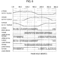
- Fig. 6 is a diagram illustrating a driving method of the inverter device according to the second embodiment of the present invention.
- the driving method is a method in which, in relation to minimal voltages of three-phase (a U phase, a V phase, and a W phase) output voltages output from the inverter device, only a single phase is affixed to a DC low potential side, and other two phases are PWM-driven, during a predetermined time period.
- the U-phase output voltage is affixed to the minimal voltage of the DC low potential side during a time period of 120 degrees from the phase angle 210 degrees to the phase angle 330 degrees
- the V-phase output voltage is affixed to the minimal voltage of the DC low potential side during a time period from the phase angle 0 degrees to the phase angle 90 degrees and from the phase angle 330 degrees to the phase angle 360 degrees
- the W-phase output voltage is affixed to the minimal voltage of the DC low potential side during a time period from the phase angle 90 degrees to the phase angle 210 degrees.
- the other two phases are PWM-driven such that inter-phase voltages of three phases are a sinusoidal wave.
- the above-described driving method is referred to as a "lower affixing two-phase modulation".
- the minimal voltage of the DC low potential side indicates a potential of low potential side 5a of the power supply voltage (a terminal voltage of the smoothing capacitor) which is converted into DC by smoothing capacitor 5 shown in Fig. 1 .
- driving pulses of switching elements 22, 23 and 24 of the upper arm switching circuit are output for the U-phase upper driving, the V-phase upper driving, and the W-phase upper driving in Fig. 6 .
- driving pulses of switching elements 25, 26 and 27 of the lower arm switching circuit are output for the U-phase lower driving, the V-phase lower driving, and the W-phase lower driving in Fig. 6 .
- power of a desired output frequency is output from inverter device 2, and drives motor 3 which is a load.
- the three-phase output voltages which are output from the inverter device are voltages with a low potential biased to the DC low potential side.
- conduction (turned-on) time of switching elements 25, 26 and 27 of the lower arm switching circuit is a larger value than conduction (turned-on) time of switching elements 22, 23 and 24 of the upper arm switching circuit.
- a conduction (turned-on) loss of the current-driven switching elements of the lower arm switching circuit is lower than a conduction (turned-on) loss of the voltage-driven switching elements of the upper arm switching circuit. For this reason, it is possible to reduce the circuit loss by shortening the conduction (turned-on) time of the upper arm switching circuit having the higher conduction (turned-on) loss. As a result, it is possible to implement an inverter device where the circuit loss is reduced by the PWM driving method.
- the inverter device relates to a driving method in a case where the voltage-driven switching elements of the upper arm switching circuit has a lower conduction (turned-on) loss than the current-driven switching elements of the lower arm switching circuit.
- Fig. 7 is a diagram illustrating a driving method of the inverter device according to another example of the second embodiment of the present invention.
- the driving method is a method in which, in relation to maximal voltages of three-phase (a U phase, a V phase, and a W phase) output voltages output from the inverter device, only a single phase is affixed to a DC high potential side, and other two phases are PWM-driven, during a predetermined time period.
- the U-phase output voltage is affixed to the maximal voltage of the DC high potential side during a time period of 120 degrees from the phase angle 30 degrees to the phase angle 150 degrees
- the V-phase output voltage is affixed to the maximal voltage of the DC high potential side during a time period from the phase angle 150 degrees to the phase angle 270 degrees
- the W-phase output voltage is affixed to the maximal voltage of the DC high potential side during a time period from the phase angle 0 degrees to the phase angle 30 degrees and from the phase angle 270 degrees to the phase angle 360 degrees.
- the other two phases are PWM-driven such that inter-phase voltages of three phases are a sinusoidal wave.
- the above-described driving method is referred to as an "upper affixing two-phase modulation".
- the maximal voltage of the DC low potential side indicates a potential of high potential side 5b of the power supply voltage (a terminal voltage of the smoothing capacitor) which is converted into DC by smoothing capacitor 5 shown in Fig. 1 .
- driving pulses of switching elements 22, 23 and 24 of the upper arm switching circuit are output for the U-phase upper driving, the V-phase upper driving, and the W-phase, upper driving in Fig. 7 .
- driving pulses of switching elements 25, 26 and 27 of the lower arm switching circuit are output for the U-phase lower driving, the V-phase lower driving, and the W-phase lower driving in Fig. 7 .
- a conduction (turned-on) loss of the current-driven switching elements of the lower arm switching circuit is higher than a conduction (turned-on) loss of the voltage-driven switching elements of the upper arm switching circuit. For this reason, it is possible to reduce the circuit loss by shortening the conduction (turned-on) time of the lower arm switching circuit having the higher conduction (turned-on) loss. As a result, it is possible to implement an inverter device where the circuit loss is reduced by the PWM driving method.
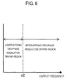
- Fig. 8 is a diagram illustrating an output frequency for changing driving methods of the inverter device according to the second embodiment of the present invention.
- a case where the voltage-driven switching elements of the upper arm switching circuit have a lower conduction (turned-on) loss than the current-driven switching elements of the lower arm switching circuit will be described as an example.
- the inverter device in a case where an AC frequency output by the inverter device is equal to or less than predetermined output frequency s2, the inverter device is PWM-driven by the above-described lower affixing two-phase modulation where the minimal voltages of the three-phase output voltages shown in Fig. 6 are affixed to the DC low potential side.
- the inverter device in a case where an AC frequency output by the inverter device exceeds predetermined output frequency s2, the inverter device is PWM-driven by the above-described upper affixing two-phase modulation where the maximal voltages of the three-phase output voltages shown in Fig. 7 are affixed to the DC high potential side.
- the predetermined output frequency s2 is an output frequency where a voltage of the capacitor of the bootstrap circuit is the same as a driving voltage for driving the switching elements of the upper arm switching circuit via the upper arm driver circuit.
- Bootstrap circuit forming driving circuit 21 of the inverter device of the present embodiment accumulates charge in capacitor 31 for a time when the lower arm switching circuit is conducted (turned on), and drives the switching elements of the upper arm switching circuit at a predetermined carrier frequency using the accumulated charge.
- the voltage of capacitor 31 is lowered since the switching elements of the upper arm switching circuit are continuously conducted (turned on). Therefore, in order to prevent the voltage of capacitor 31 from being lowered, the lower affixing two-phase modulation is performed in which other two phases are PWM-driven during a time period when an output voltage of one phase of three phases is affixed to the DC low potential side which is a minimal voltage, in a case where an output frequency is equal to or less than predetermined output frequency s2. Thereby, the switching elements of the upper arm switching circuit can be stabilized and be driven.
- the inverter device is preferably driven using the upper affixing two-phase modulation. Thereby, it is possible to implement an inverter device having a low circuit loss.
- a change between the lower affixing two-phase modulation and the upper affixing two-phase modulation is made at predetermined output frequency s2 in the inverter device, and thereby the inverter device can be driven in a state where the circuit loss is low over the full range of the output frequency.
- the driving circuit is constituted by the bootstrap circuit using different kinds of switching elements, the voltage-driven switching elements for the upper arm switching circuit and the current-driven switching elements for the lower arm switching circuit, thereby achieving simplification of the driving circuit and low costs.
- an optimal driving control by changing the driving methods of the switching elements at a predetermined output frequency, it is possible to implement an inverter device having improved efficiency along with stable driving by reducing circuit loss.
- Fig. 9 is a cutaway perspective view illustrating an outline of the vacuum cleaner according to the third embodiment of the present invention.
- the embodiment has the inverter device described in the first embodiment or the second embodiment embedded therein, and is used as a driving device of a motor for the fan of the vacuum cleaner.
- the vacuum cleaner outputs AC power, which is input via power receptacle 92, at a predetermined output frequency via the inverter device, and drives, for example, motor 91 for a fan such as an inverter fan motor, inside vacuum cleaner main body 90.
- the fan rotates at a predetermined rotation rate, and the vacuum cleaner suctions dust and the like.
- the high efficiency inverter device is incorporated at low costs, and thereby it is possible to implement a vacuum cleaner having high efficiency, high reliability, and high suction power, with a low cost configuration.
- the inverter device may be used for a driving device of a motor of an electric washing machine, an air conditioner, a refrigerator or a power apparatus, and the same effects can be achieved.
- gallium nitride GaN
- IGBT gallium nitride
- the present invention is not limited thereto.
- a MOSFET element may be used as the voltage-driven switching element
- a semiconductor element such as a bipolar transistor element may be used as the current-driven switching element.
- the present invention may be widely applied to an inverter device requiring high efficiency and high reliability, and to an electric apparatus such as a vacuum cleaner using the same.
Landscapes
- Engineering & Computer Science (AREA)
- Power Engineering (AREA)
- Inverter Devices (AREA)
- Electric Suction Cleaners (AREA)
- Electric Vacuum Cleaner (AREA)
- Control Of Ac Motors In General (AREA)
- Power Conversion In General (AREA)
- Rectifiers (AREA)
Applications Claiming Priority (2)
| Application Number | Priority Date | Filing Date | Title |
|---|---|---|---|
| JP2010069651A JP5494095B2 (ja) | 2010-03-25 | 2010-03-25 | インバータ装置およびそれをファンモータの駆動装置に用いた電気掃除機 |
| PCT/JP2010/004404 WO2011117932A1 (ja) | 2010-03-25 | 2010-07-06 | インバータ装置およびそれを用いた電気機器 |
Publications (2)
| Publication Number | Publication Date |
|---|---|
| EP2552008A1 true EP2552008A1 (de) | 2013-01-30 |
| EP2552008A4 EP2552008A4 (de) | 2017-11-15 |
Family
ID=44672531
Family Applications (1)
| Application Number | Title | Priority Date | Filing Date |
|---|---|---|---|
| EP10848326.4A Withdrawn EP2552008A4 (de) | 2010-03-25 | 2010-07-06 | Umrichtervorrichtung und elektrische vorrichtung damit |
Country Status (5)
| Country | Link |
|---|---|
| US (1) | US20120212170A1 (de) |
| EP (1) | EP2552008A4 (de) |
| JP (1) | JP5494095B2 (de) |
| CN (1) | CN102835017B (de) |
| WO (1) | WO2011117932A1 (de) |
Cited By (2)
| Publication number | Priority date | Publication date | Assignee | Title |
|---|---|---|---|---|
| JP2016092920A (ja) * | 2014-10-31 | 2016-05-23 | 三菱電機株式会社 | 電動送風機及び電気掃除機 |
| US12027997B2 (en) | 2018-12-26 | 2024-07-02 | Samsung Electronics Co., Ltd. | Inverter and refrigerator including inverter |
Families Citing this family (14)
| Publication number | Priority date | Publication date | Assignee | Title |
|---|---|---|---|---|
| JP2013128356A (ja) * | 2011-12-19 | 2013-06-27 | Panasonic Corp | モータインバータ装置 |
| JP5857189B2 (ja) * | 2011-12-27 | 2016-02-10 | パナソニックIpマネジメント株式会社 | インバータ装置 |
| JP5997567B2 (ja) * | 2012-10-03 | 2016-09-28 | 日立アプライアンス株式会社 | モータ制御装置及び空気調和機 |
| CN105765847B (zh) * | 2013-11-29 | 2018-12-25 | 新电元工业株式会社 | 逆变器装置 |
| JP6194812B2 (ja) * | 2014-02-18 | 2017-09-13 | トヨタ自動車株式会社 | 半導体モジュール |
| US20180152080A1 (en) * | 2015-05-29 | 2018-05-31 | Nidec Corporation | Dc-brushless-motor control device |
| WO2017038214A1 (ja) * | 2015-08-28 | 2017-03-09 | 富士電機株式会社 | 半導体装置 |
| JP6607137B2 (ja) * | 2016-04-21 | 2019-11-20 | 株式会社デンソー | 蓄電装置 |
| JP6576371B2 (ja) | 2017-01-13 | 2019-09-18 | ミネベアミツミ株式会社 | モータ駆動制御装置 |
| JP7100562B2 (ja) * | 2018-11-05 | 2022-07-13 | 株式会社Soken | 駆動システム |
| CN110011549A (zh) * | 2019-01-21 | 2019-07-12 | 关键禾芯科技股份有限公司 | 调压整流电路系统 |
| CN112751493B (zh) * | 2019-10-29 | 2025-02-18 | 日本电产株式会社 | 电力变换装置和电气设备 |
| CN111106785B (zh) * | 2019-12-31 | 2022-06-14 | 无锡同方聚能控制科技有限公司 | 一种电器故障提示的电机控制方法 |
| JP2024094083A (ja) * | 2022-12-27 | 2024-07-09 | オムロン株式会社 | インバータ、インバータの制御方法及びプログラム |
Family Cites Families (14)
| Publication number | Priority date | Publication date | Assignee | Title |
|---|---|---|---|---|
| JPS63262062A (ja) * | 1987-04-17 | 1988-10-28 | Fuji Electric Co Ltd | インバ−タの主回路 |
| JPH0662037B2 (ja) | 1987-11-11 | 1994-08-17 | 旭精密株式会社 | 表示間隔切換機能を有するデジタル表示製図機 |
| JPH0731182A (ja) * | 1993-07-12 | 1995-01-31 | Sharp Corp | 直流電動機駆動用インバータ制御回路 |
| US7053587B2 (en) * | 2004-02-10 | 2006-05-30 | Denso Corporation | Apparatus for controlling three-phase AC motor on two-phase modulation technique |
| JP4801905B2 (ja) * | 2005-01-11 | 2011-10-26 | アルプス電気株式会社 | モータ駆動制御装置 |
| JP4492371B2 (ja) * | 2005-02-01 | 2010-06-30 | パナソニック株式会社 | インバータ制御方法 |
| JP4300209B2 (ja) * | 2005-11-04 | 2009-07-22 | 東芝キヤリア株式会社 | インバータ装置 |
| JP2007318891A (ja) * | 2006-05-25 | 2007-12-06 | Toyota Industries Corp | スイッチング素子駆動用電源回路 |
| JP4799512B2 (ja) * | 2007-08-31 | 2011-10-26 | 三菱電機株式会社 | 電力変換装置およびその装置を用いた空気調和機 |
| JP4528321B2 (ja) * | 2007-09-26 | 2010-08-18 | シャープ株式会社 | スイッチング回路、回路、並びにスイッチング回路及び駆動パルス生成回路を含む回路 |
| CN100566111C (zh) * | 2007-10-30 | 2009-12-02 | 黑龙江工商职业技术学院 | 一种六开关五电平电压源型逆变装置及其控制方法 |
| JP5433214B2 (ja) * | 2007-12-07 | 2014-03-05 | パナソニック株式会社 | モータ駆動回路 |
| JP2010051165A (ja) * | 2008-07-24 | 2010-03-04 | Panasonic Corp | 半導体装置のゲート駆動回路及びそれを用いた電力変換装置 |
| JP2010035387A (ja) * | 2008-07-31 | 2010-02-12 | Daikin Ind Ltd | 電圧形駆動素子のゲート駆動装置 |
-
2010
- 2010-03-25 JP JP2010069651A patent/JP5494095B2/ja not_active Expired - Fee Related
- 2010-07-06 EP EP10848326.4A patent/EP2552008A4/de not_active Withdrawn
- 2010-07-06 WO PCT/JP2010/004404 patent/WO2011117932A1/ja not_active Ceased
- 2010-07-06 CN CN201080065757.9A patent/CN102835017B/zh not_active Expired - Fee Related
- 2010-07-06 US US13/505,353 patent/US20120212170A1/en not_active Abandoned
Non-Patent Citations (1)
| Title |
|---|
| See references of WO2011117932A1 * |
Cited By (2)
| Publication number | Priority date | Publication date | Assignee | Title |
|---|---|---|---|---|
| JP2016092920A (ja) * | 2014-10-31 | 2016-05-23 | 三菱電機株式会社 | 電動送風機及び電気掃除機 |
| US12027997B2 (en) | 2018-12-26 | 2024-07-02 | Samsung Electronics Co., Ltd. | Inverter and refrigerator including inverter |
Also Published As
| Publication number | Publication date |
|---|---|
| CN102835017B (zh) | 2015-04-29 |
| CN102835017A (zh) | 2012-12-19 |
| JP2011205764A (ja) | 2011-10-13 |
| WO2011117932A1 (ja) | 2011-09-29 |
| US20120212170A1 (en) | 2012-08-23 |
| JP5494095B2 (ja) | 2014-05-14 |
| EP2552008A4 (de) | 2017-11-15 |
Similar Documents
| Publication | Publication Date | Title |
|---|---|---|
| EP2552008A1 (de) | Umrichtervorrichtung und elektrische vorrichtung damit | |
| CN108370223B (zh) | 电力转换装置 | |
| US11258391B2 (en) | Rotating electrical machine control device | |
| US8836258B2 (en) | Inverter device, motor driving device, refrigerating air conditioner, and power generation system | |
| US10312827B2 (en) | Power conversion device | |
| US8217602B2 (en) | Motor driving apparatus and control method thereof | |
| JP6402828B2 (ja) | 充電共用インバータ | |
| CN112534709A (zh) | 旋转电机控制装置 | |
| CN114946116B (zh) | 旋转电机控制装置 | |
| Lee et al. | GaN-based single phase brushless DC motor drive for high-speed applications | |
| CN1989685B (zh) | 具有电源侧四象限变流器的牵引变流器 | |
| WO2022153614A1 (ja) | マルチレベルインバータ | |
| JP5788540B2 (ja) | 電動機駆動装置、及び冷凍空調装置 | |
| US10050569B2 (en) | Inverter control device and inverter control method | |
| JP5647558B2 (ja) | インバータ装置 | |
| US11444530B2 (en) | Regenerative undeland snubber circuit for half-arm of an inverter | |
| WO2014024596A1 (ja) | インバータ駆動回路 | |
| JP2016001991A (ja) | 電動機駆動装置、及び冷凍空調装置 | |
| JP5857189B2 (ja) | インバータ装置 | |
| JP2007244183A (ja) | 単相倍電圧整流回路およびインバータ装置 | |
| JP2024104700A (ja) | 充電制御方法、充電制御装置、及び、電源回路 | |
| KR20230097159A (ko) | 인버터, 전기 구동 장치, 차량 및 인버터의 제어 가능한 스위치를 제어하는 방법 및 대응하는 컴퓨터 프로그램 제품 | |
| JP2014212588A (ja) | 電源装置およびそれを搭載した電気電子機器 |
Legal Events
| Date | Code | Title | Description |
|---|---|---|---|
| PUAI | Public reference made under article 153(3) epc to a published international application that has entered the european phase |
Free format text: ORIGINAL CODE: 0009012 |
|
| 17P | Request for examination filed |
Effective date: 20120426 |
|
| AK | Designated contracting states |
Kind code of ref document: A1 Designated state(s): AL AT BE BG CH CY CZ DE DK EE ES FI FR GB GR HR HU IE IS IT LI LT LU LV MC MK MT NL NO PL PT RO SE SI SK SM TR |
|
| DAX | Request for extension of the european patent (deleted) | ||
| RA4 | Supplementary search report drawn up and despatched (corrected) |
Effective date: 20171012 |
|
| RIC1 | Information provided on ipc code assigned before grant |
Ipc: H02P 27/06 20060101ALI20171006BHEP Ipc: H02M 1/00 20070101ALI20171006BHEP Ipc: H02M 7/5387 20070101AFI20171006BHEP Ipc: H02P 27/08 20060101ALI20171006BHEP Ipc: A47L 9/00 20060101ALI20171006BHEP Ipc: A47L 9/28 20060101ALI20171006BHEP Ipc: H02M 7/5388 20070101ALI20171006BHEP Ipc: H02M 1/08 20060101ALI20171006BHEP Ipc: H02M 7/48 20070101ALI20171006BHEP Ipc: H02M 1/084 20060101ALI20171006BHEP |
|
| STAA | Information on the status of an ep patent application or granted ep patent |
Free format text: STATUS: REQUEST FOR EXAMINATION WAS MADE |
|
| STAA | Information on the status of an ep patent application or granted ep patent |
Free format text: STATUS: THE APPLICATION IS DEEMED TO BE WITHDRAWN |
|
| 18D | Application deemed to be withdrawn |
Effective date: 20180515 |