EP2551903B1 - Gehäuse für lichtemittierende Vorrichtung und Beleuchtungssystem damit - Google Patents
Gehäuse für lichtemittierende Vorrichtung und Beleuchtungssystem damit Download PDFInfo
- Publication number
- EP2551903B1 EP2551903B1 EP12160393.0A EP12160393A EP2551903B1 EP 2551903 B1 EP2551903 B1 EP 2551903B1 EP 12160393 A EP12160393 A EP 12160393A EP 2551903 B1 EP2551903 B1 EP 2551903B1
- Authority
- EP
- European Patent Office
- Prior art keywords
- light emitting
- emitting device
- disposed
- cavity
- layer
- Prior art date
- Legal status (The legal status is an assumption and is not a legal conclusion. Google has not performed a legal analysis and makes no representation as to the accuracy of the status listed.)
- Active
Links
Images


Classifications
-
- H—ELECTRICITY
- H01—ELECTRIC ELEMENTS
- H01L—SEMICONDUCTOR DEVICES NOT COVERED BY CLASS H10
- H01L33/00—Semiconductor devices with at least one potential-jump barrier or surface barrier specially adapted for light emission; Processes or apparatus specially adapted for the manufacture or treatment thereof or of parts thereof; Details thereof
- H01L33/48—Semiconductor devices with at least one potential-jump barrier or surface barrier specially adapted for light emission; Processes or apparatus specially adapted for the manufacture or treatment thereof or of parts thereof; Details thereof characterised by the semiconductor body packages
- H01L33/62—Arrangements for conducting electric current to or from the semiconductor body, e.g. lead-frames, wire-bonds or solder balls
-
- H—ELECTRICITY
- H01—ELECTRIC ELEMENTS
- H01L—SEMICONDUCTOR DEVICES NOT COVERED BY CLASS H10
- H01L33/00—Semiconductor devices with at least one potential-jump barrier or surface barrier specially adapted for light emission; Processes or apparatus specially adapted for the manufacture or treatment thereof or of parts thereof; Details thereof
-
- H—ELECTRICITY
- H01—ELECTRIC ELEMENTS
- H01L—SEMICONDUCTOR DEVICES NOT COVERED BY CLASS H10
- H01L25/00—Assemblies consisting of a plurality of individual semiconductor or other solid state devices ; Multistep manufacturing processes thereof
- H01L25/03—Assemblies consisting of a plurality of individual semiconductor or other solid state devices ; Multistep manufacturing processes thereof all the devices being of a type provided for in the same subgroup of groups H01L27/00 - H01L33/00, or in a single subclass of H10K, H10N, e.g. assemblies of rectifier diodes
- H01L25/04—Assemblies consisting of a plurality of individual semiconductor or other solid state devices ; Multistep manufacturing processes thereof all the devices being of a type provided for in the same subgroup of groups H01L27/00 - H01L33/00, or in a single subclass of H10K, H10N, e.g. assemblies of rectifier diodes the devices not having separate containers
- H01L25/075—Assemblies consisting of a plurality of individual semiconductor or other solid state devices ; Multistep manufacturing processes thereof all the devices being of a type provided for in the same subgroup of groups H01L27/00 - H01L33/00, or in a single subclass of H10K, H10N, e.g. assemblies of rectifier diodes the devices not having separate containers the devices being of a type provided for in group H01L33/00
- H01L25/0753—Assemblies consisting of a plurality of individual semiconductor or other solid state devices ; Multistep manufacturing processes thereof all the devices being of a type provided for in the same subgroup of groups H01L27/00 - H01L33/00, or in a single subclass of H10K, H10N, e.g. assemblies of rectifier diodes the devices not having separate containers the devices being of a type provided for in group H01L33/00 the devices being arranged next to each other
-
- H—ELECTRICITY
- H01—ELECTRIC ELEMENTS
- H01L—SEMICONDUCTOR DEVICES NOT COVERED BY CLASS H10
- H01L33/00—Semiconductor devices with at least one potential-jump barrier or surface barrier specially adapted for light emission; Processes or apparatus specially adapted for the manufacture or treatment thereof or of parts thereof; Details thereof
- H01L33/48—Semiconductor devices with at least one potential-jump barrier or surface barrier specially adapted for light emission; Processes or apparatus specially adapted for the manufacture or treatment thereof or of parts thereof; Details thereof characterised by the semiconductor body packages
- H01L33/483—Containers
- H01L33/486—Containers adapted for surface mounting
-
- F—MECHANICAL ENGINEERING; LIGHTING; HEATING; WEAPONS; BLASTING
- F21—LIGHTING
- F21K—NON-ELECTRIC LIGHT SOURCES USING LUMINESCENCE; LIGHT SOURCES USING ELECTROCHEMILUMINESCENCE; LIGHT SOURCES USING CHARGES OF COMBUSTIBLE MATERIAL; LIGHT SOURCES USING SEMICONDUCTOR DEVICES AS LIGHT-GENERATING ELEMENTS; LIGHT SOURCES NOT OTHERWISE PROVIDED FOR
- F21K9/00—Light sources using semiconductor devices as light-generating elements, e.g. using light-emitting diodes [LED] or lasers
- F21K9/20—Light sources comprising attachment means
- F21K9/23—Retrofit light sources for lighting devices with a single fitting for each light source, e.g. for substitution of incandescent lamps with bayonet or threaded fittings
-
- F—MECHANICAL ENGINEERING; LIGHTING; HEATING; WEAPONS; BLASTING
- F21—LIGHTING
- F21V—FUNCTIONAL FEATURES OR DETAILS OF LIGHTING DEVICES OR SYSTEMS THEREOF; STRUCTURAL COMBINATIONS OF LIGHTING DEVICES WITH OTHER ARTICLES, NOT OTHERWISE PROVIDED FOR
- F21V29/00—Protecting lighting devices from thermal damage; Cooling or heating arrangements specially adapted for lighting devices or systems
- F21V29/15—Thermal insulation
-
- F—MECHANICAL ENGINEERING; LIGHTING; HEATING; WEAPONS; BLASTING
- F21—LIGHTING
- F21Y—INDEXING SCHEME ASSOCIATED WITH SUBCLASSES F21K, F21L, F21S and F21V, RELATING TO THE FORM OR THE KIND OF THE LIGHT SOURCES OR OF THE COLOUR OF THE LIGHT EMITTED
- F21Y2105/00—Planar light sources
- F21Y2105/10—Planar light sources comprising a two-dimensional array of point-like light-generating elements
-
- F—MECHANICAL ENGINEERING; LIGHTING; HEATING; WEAPONS; BLASTING
- F21—LIGHTING
- F21Y—INDEXING SCHEME ASSOCIATED WITH SUBCLASSES F21K, F21L, F21S and F21V, RELATING TO THE FORM OR THE KIND OF THE LIGHT SOURCES OR OF THE COLOUR OF THE LIGHT EMITTED
- F21Y2115/00—Light-generating elements of semiconductor light sources
- F21Y2115/10—Light-emitting diodes [LED]
-
- H—ELECTRICITY
- H01—ELECTRIC ELEMENTS
- H01L—SEMICONDUCTOR DEVICES NOT COVERED BY CLASS H10
- H01L2224/00—Indexing scheme for arrangements for connecting or disconnecting semiconductor or solid-state bodies and methods related thereto as covered by H01L24/00
- H01L2224/01—Means for bonding being attached to, or being formed on, the surface to be connected, e.g. chip-to-package, die-attach, "first-level" interconnects; Manufacturing methods related thereto
- H01L2224/10—Bump connectors; Manufacturing methods related thereto
- H01L2224/15—Structure, shape, material or disposition of the bump connectors after the connecting process
- H01L2224/16—Structure, shape, material or disposition of the bump connectors after the connecting process of an individual bump connector
-
- H—ELECTRICITY
- H01—ELECTRIC ELEMENTS
- H01L—SEMICONDUCTOR DEVICES NOT COVERED BY CLASS H10
- H01L25/00—Assemblies consisting of a plurality of individual semiconductor or other solid state devices ; Multistep manufacturing processes thereof
- H01L25/16—Assemblies consisting of a plurality of individual semiconductor or other solid state devices ; Multistep manufacturing processes thereof the devices being of types provided for in two or more different main groups of groups H01L27/00 - H01L33/00, or in a single subclass of H10K, H10N, e.g. forming hybrid circuits
- H01L25/167—Assemblies consisting of a plurality of individual semiconductor or other solid state devices ; Multistep manufacturing processes thereof the devices being of types provided for in two or more different main groups of groups H01L27/00 - H01L33/00, or in a single subclass of H10K, H10N, e.g. forming hybrid circuits comprising optoelectronic devices, e.g. LED, photodiodes
-
- H—ELECTRICITY
- H01—ELECTRIC ELEMENTS
- H01L—SEMICONDUCTOR DEVICES NOT COVERED BY CLASS H10
- H01L2924/00—Indexing scheme for arrangements or methods for connecting or disconnecting semiconductor or solid-state bodies as covered by H01L24/00
- H01L2924/10—Details of semiconductor or other solid state devices to be connected
- H01L2924/11—Device type
- H01L2924/13—Discrete devices, e.g. 3 terminal devices
- H01L2924/1301—Thyristor
-
- H—ELECTRICITY
- H01—ELECTRIC ELEMENTS
- H01L—SEMICONDUCTOR DEVICES NOT COVERED BY CLASS H10
- H01L33/00—Semiconductor devices with at least one potential-jump barrier or surface barrier specially adapted for light emission; Processes or apparatus specially adapted for the manufacture or treatment thereof or of parts thereof; Details thereof
- H01L33/36—Semiconductor devices with at least one potential-jump barrier or surface barrier specially adapted for light emission; Processes or apparatus specially adapted for the manufacture or treatment thereof or of parts thereof; Details thereof characterised by the electrodes
- H01L33/40—Materials therefor
- H01L33/405—Reflective materials
-
- H—ELECTRICITY
- H01—ELECTRIC ELEMENTS
- H01L—SEMICONDUCTOR DEVICES NOT COVERED BY CLASS H10
- H01L33/00—Semiconductor devices with at least one potential-jump barrier or surface barrier specially adapted for light emission; Processes or apparatus specially adapted for the manufacture or treatment thereof or of parts thereof; Details thereof
- H01L33/48—Semiconductor devices with at least one potential-jump barrier or surface barrier specially adapted for light emission; Processes or apparatus specially adapted for the manufacture or treatment thereof or of parts thereof; Details thereof characterised by the semiconductor body packages
- H01L33/58—Optical field-shaping elements
- H01L33/60—Reflective elements
-
- H—ELECTRICITY
- H01—ELECTRIC ELEMENTS
- H01L—SEMICONDUCTOR DEVICES NOT COVERED BY CLASS H10
- H01L33/00—Semiconductor devices with at least one potential-jump barrier or surface barrier specially adapted for light emission; Processes or apparatus specially adapted for the manufacture or treatment thereof or of parts thereof; Details thereof
- H01L33/48—Semiconductor devices with at least one potential-jump barrier or surface barrier specially adapted for light emission; Processes or apparatus specially adapted for the manufacture or treatment thereof or of parts thereof; Details thereof characterised by the semiconductor body packages
- H01L33/64—Heat extraction or cooling elements
- H01L33/642—Heat extraction or cooling elements characterized by the shape
Definitions
- the present invention relates to a light emitting device package and a lighting system including the same.
- LEDs light emitting diodes
- LEDs are semiconductor devices that convert electric energy into light and extensively used as next-generation light sources in place of conventional fluorescent lamps and glow lamps.
- the LED Since the LED generates the light by using the semiconductor device, the LED may represent low power consumption as compared with the glow lamp that generates the light by heating tungsten or the fluorescent lamp that generates the light by urging ultraviolet ray, which is generated through the high-voltage discharge, to collide with a fluorescent substance.
- the LED generates the light by using the potential gap of the semiconductor device, so the LED is advantageous as compared with conventional light sources in terms of life span, response speed, safety and environmental-friendly requirement.
- the LEDs are increasingly used as light sources for lighting devices, such as various lamps used indoors and outdoors, liquid crystal displays, electric signboards, and street lamps.
- JP 2007 214474 A discloses an edgelight formed with lead frames each having an unevenness and cut into a rod shape.
- the lead frames are integrated with a metal plate and insulated from each other via a heat conductive resin. LEDs are mounted on the cut surface for each line of the concave portions of the lead frames.
- WO 2004/107443 A1 discloses an insulated metal substrate, comprising a metal substrate, an insulation layer, electrical tracks, provided on the insulation layer, to which light diodes are connected.
- the metal substrate comprises recesses receiving the light diodes and serving as reflectors.
- WO 2010/140693 A1 discloses an electronic component with a frame, an LED mounted on the frame and a resist layer for adhering frame sections to each other.
- KR 10 1051065 discloses a light emitting device package with increased heat dissipation efficiency including a plurality of cavities formed in a body, wherein one LED is arranged in each cavity and one lead frame fully covers the base and side surfaces of the cavity. The LEDs arranged in different cavities are connected in series using wire bonding.
- the present invention provides a light emitting device package including light emitting devices, which are flip-bonded to bottoms of cavities formed at different regions of a body, as defined in claim 1, and a lighting system including the same, as defined in claim 13.
- the present invention provides a light emitting device package, in which a plurality of lead frames are disposed in a plurality of cavities and light emitting devices are flip-bonded to the lead frames disposed on bottoms of the cavities, as defined in claim 1, and a lighting system including the same, as defined in claim 13.
- a light emitting device package according to the present invention is defined in claim 1 Embodiments of the light emitting device package are further defined in claims 2-12.
- a lighting system includes a plurality of light emitting device packages as outlined above; and a module substrate where the light emitting device packages are arrayed.
- Each light emitting device package includes a body; a first cavity in a first region of the body; a second cavity in a second region of the body; first and second lead frames on a bottom surface of the first cavity; third and fourth lead frames on a bottom surface of the second cavity; a first light emitting device flip-bonded to the first and second lead frames in the first cavity; a second light emitting device flip-bonded to the third and fourth lead frames in the second cavity; and a molding member in the first and second cavities.
- FIG. 1 is a perspective view showing a light emitting device package according to the present invention
- FIG. 2 is a plan view of the light emitting device package shown in FIG. 1
- FIG. 3 is a plan view showing a light emitting device connected to a lead frame of the light emitting device package shown in FIG. 1
- FIG. 4 is a lower view showing the light emitting device package of FIG. 1
- FIG. 5 is a side sectional view showing the light emitting device package of FIG. 1 .
- the light emitting device package 100 includes a body 110, a first cavity 125 formed at a first region of the body 110, a second cavity 135 formed at a second region of the body 110, a plurality of lead frames having first to third lead frames 121, 131 and 141 disposed in the body 110, and first and second light emitting devices 151 and 152.
- the body 110 includes an insulating material and may include a conductive material.
- the body 110 includes at least one of a resin material, such as PPA (Polyphthalamide), a Si-based material, a metallic material, PSG (photosensitive glass), Al 2 O 3 , and PCB.
- the body 110 may include a resin material having a high reflectivity, such as PPA (Polyphthalamide).
- the body 110 can be formed by using a material having electric conductivity.
- an insulating layer (not shown) is formed on a surface of the body 110 to prevent the electric short between the body 110 and the first to third lead frames 121, 131 and 141.
- the body 110 may have various external shapes, such as a triangle, a rectangle, a polygon and a circle according to the application and the design of the light emitting device package 100.
- the body 110 includes a plurality of lateral sides 111 to 114, in which at least one of the lateral sides 111 to 114 is vertical or inclined to a lower surface of the body 110.
- the lateral sides 111 to 114 of the body 110 may be vertical or inclined to the lower surface of the body 110 and widths of the first and second lateral sides 111 and 112 may be different from widths of the third and fourth lateral sides 113 and 114.
- the widths of the first and second lateral sides 111 and 112 may correspond to the distance between the third and fourth lateral sides 113 and 114 and the widths of the third and fourth lateral sides 113 and 114 may correspond to the distance between the first and second lateral sides 111 and 112.
- the body 110 has a polygonal structure, for instance, a hexahedral structure, but the present invention is not limited thereto.
- An upper portion 116 of the body 110 is formed with a first region defined by an upper portion of the first cavity 125 and a second region defined by an upper portion of the second cavity 135 and the light is emitted through the first and second regions.
- the first and second cavities 125 and 135 are disposed between a top surface and a lower surface of the body 110.
- the first and second cavities 125 and 135 are disposed at different regions in the body 110 and concaved down from the top surface of the body 110 so that the first and second cavities 125 and 135 have the cup shape or the recess shape.
- Lateral sides of the first cavity 125 are inclined or vertical to the bottom surface of the first cavity 125.
- two opposite lateral sides may be inclined in the same angle or different angles.
- the center of the first cavity 125 may be aligned in line with the center of the second cavity 135 in the length direction of the light emitting device package.
- the first lead frame 121 and a first part 132 of the second lead frame 131 are disposed in the first cavity 125 while being spaced apart from each other.
- the first lead frame 121 and the first part 132 of the second lead frame 131 are disposed on the bottom surface of in the first cavity 125 to serve as a heat dissipation part.
- a first separation part 126 separates the first lead frame 121 and the first part 132 of the second lead frame 131 disposed on the bottom surface of in the first cavity 125 from each other as shown in FIG. 2 .
- the first lead frame 121 and the first part 132 of the second lead frame 131 may constitute the structure of the first cavity 125.
- the first separation part 126 is disposed on the bottom surface and the lateral sides of the first cavity 125.
- the third lead frame 141 and a second part 134 of the second lead frame 131 are disposed in the second cavity 135 while being spaced apart from each other.
- the third lead frame 141 and the second part 134 of the second lead frame 131 are disposed on the bottom surface of in the second cavity 135 to serve as a heat dissipation part.
- a second separation part 136 separates third lead frame 141 and the second part 134 of the second lead frame 131 disposed on the bottom surface of in the second cavity 135 from each other as shown in FIG. 2 .
- the third lead frame 141 and the second part 134 of the second lead frame 131 may constitute the structure of the second cavity 135.
- the second separation part 136 is provided on the bottom surface and the lateral sides of the second cavity 135.
- the first and second separation parts 126 and 136 are formed by using a material the same as that of the body 110.
- the first and second separation parts 126 and 136 may have the same width.
- the second lead frame 131 is disposed between the first lead frame 121 and the third lead frame 141.
- the length D2 of the first lead frame 121 may be equal to the length D4 of the third lead frame 141 and shorter than the length D3 of the second lead frame 131.
- the length direction refers to the direction extending through the centers of the first and second cavities 125 and 135 or along the long lateral sides of the light emitting device package.
- the width direction refers to the direction extending perpendicularly to the length direction or along the short lateral sides of the light emitting device package.
- the first to third lead frames 121, 131 and 141 may have the same width D1.
- the thickness of the first to third lead frames 121, 131 and 141 is in the range of about 0.15mm to about 0.3mm. Since the first and second lead frames 121 and 131 in the first cavity 125 and the second and third lead frames 131 and 141 in the second cavity 135 are directly connected to the light emitting devices 151 and 152, respectively, the heat dissipation efficiency can be improved.
- the first to third lead frames 121, 131 and 141 include conductive metallic materials.
- the first to third lead frames 121, 131 and 141 may include at least one selected from the group consisting of Ti, Cu, Ni, Au, Cr, Ta, Pt, Sn, Ag, P and an alloy thereof.
- the first to third lead frames 121, 131 and 141 can be formed of homogeneous metal layers or heterogeneous metal layers, and the present invention is not limited thereto.
- upper parts 121A and 141A of the first and third lead frames 121 and 141 are bent outward of the cavities 125 and 135 and disposed between the top surface and the lower surface of the body 110 closely to the top surface of the body 110 than to the lower surface of the body 110.
- the upper part 121A of the first lead frame 121 is bent toward the first lateral side 111 of the body 110 at the lower portion of the first lateral side 111 of the body 110 and the upper part 141A of the third lead frame 141 is bent toward the second lateral side 112 of the body 110, which is opposite to the first lateral side 111 of the body 110, at the lower portion of the second lateral side 112 of the body 110.
- other parts of the first to third lead frames 121, 131 and 141 may be selectively exposed through at least one lateral side of the body 110.
- a first separation region 126A provided between the first and second lead frames 121 and 131 may have an interval equal to or different from an interval of a second separation region 136A provided between the second and third lead frames 131 and 141.
- the first and second separation regions 126A and 136A may have the length equal to the width D1 of the first to third lead frames 121, 131 and 141.
- connection part 133 of the second lead frame 131 connects the first part 132 of the second lead frame 131 to the second part 134 of the second lead frame 131. As shown in FIG. 5 , the connection part 133 may be disposed in the body 110 or exposed on the top surface of the body 110.
- the bottom surface of the first cavity 125 is aligned on the same plane with the lower surface 115 of the body 110.
- the first lead frame 121 is spaced apart from the first part 132 of the second lead frame 131 by the first separation part 126.
- the bottom surface of the second cavity 135 is aligned on the same plane with the lower surface 115 of the body 110.
- the second lead frame 131 is spaced apart from the second part 134 of the second lead frame 131 by the second separation part 136.
- At least one first light emitting device 151 is disposed in the first cavity 125 and the first light emitting device 151 is bonded to the bottom surface of the first cavity 125 through the flip scheme.
- the first light emitting device 151 can be bonded to the first lead frame 121 and the first part 132 of the second lead frame 131 by an adhesive member, such as a solder or a conductive member, without using an additional wire.
- the first cavity 125 may have the symmetrical structure about the line extending through the center of the first light emitting device 151.
- the first cavity 125 may have the point symmetrical structure or the asymmetrical structure.
- At least one second light emitting device 152 is disposed in the second cavity 135 and the second light emitting device 152 is bonded to the bottom surface of the second cavity 135.
- the second light emitting device 152 can be soldered to the third lead frame 141 and the second part 134 of the second lead frame 131 without using an additional wire.
- the light emitting devices 151 and 152 can be disposed at the centers of the cavities 125 and 135, respectively.
- the second cavity 135 may have the symmetrical structure about the line extending through the center of the second light emitting device 152.
- the second cavity 135 may have the point symmetrical structure or the asymmetrical structure.
- first and second light emitting devices 151 and 152 are flip-bonded in the first and second cavities 125 and 135, respectively, a space required for a wire bonding can be omitted in the first and second cavities 125 and 135.
- first light emitting device 151 is bonded in the first cavity 125 and the second light emitting device 152 is bonded in the second cavity 135, it is not necessary to provide an additional lead frame on the body 110, which is required for the wire bonding. Further, the thickness of the light emitting device package can be more reduced because the wire can be omitted.
- the first and second light emitting devices 151 and 152 may selectively emit the light having the wavelength band in the range of the ultraviolet band to the visible band. In addition, the first and second light emitting devices 151 and 152 may emit the lights having the same peak wavelength or the different peak wavelengths.
- the first and second light emitting devices 151 and 152 may include an LED chip employing group III-V compound semiconductors. For instance, the first and second light emitting devices 151 and 152 may include at least one of a UV (ultraviolet) LED chip, a blue LED chip, a green LED chip, a white LED chip and a red LED chip.
- a first molding member 161 is disposed in the first cavity 125 and a second molding member 162 is disposed in the second cavity 135.
- the first and second molding members 161 and 162 are formed of a transmittive resin layers including silicon or epoxy materials.
- the first and second molding members 161 and 162 can be formed up to the upper region of the body 110.
- the first and second molding members 161 and 162 may include phosphors to convert the wavelength of the light emitted from the first and second light emitting devices 151 and 152. The phosphor is excited by a part of the light emitted from the first and second light emitting devices 151 and 152 so that the wavelength of the light can be converted.
- the first and second light emitting devices 151 and 152 are blue LEDs and the phosphor is a yellow phosphor, the yellow phosphor is excited by the blue light so that the white light may be generated. If the first and second light emitting devices 151 and 152 emit the UV light, red, green and blue phosphors are added to the first and second molding members 161 and 162 to generate the white light. The same type or different types of phosphors may be added to the first and second molding members 161 and 162, and the present invention is not limited thereto.
- a lens 170 can be formed on the body 110.
- the lens may include a concave lens and/or a convex lens and can adjust the distribution of the light emitted from the light emitting device package 100.
- the lens may have a concave structure at the center thereof and a convex structure at the regions corresponding to the light emitting devices 151 and 152.
- a concave part 171 may be provided at the center of the top surface of the lens 170, but the present invention is not limited thereto.
- FIG. 7 is a perspective view showing a lead frame of a light emitting device package according to another embodiment of the present invention.
- the light emitting device package includes first and second lead frames 122 and 123 having the same length L1.
- the first and second lead frames 122 and 123 are spaced apart from each other in the first and second cavities 125 and 135 by a separation part 127.
- a side width D5 of the first lead frame 122 is wider than a side width D6 of the second lead frame 123.
- An upper part 122A of the first lead frame 122 and an upper part 123A of the second lead frame 123 are bent in opposition to each other.
- the separation part 127 extends lengthwise along the first and second lead frames 122 and 123 by way of the bottom surfaces of the first and second cavities 125 and 135.
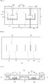
- the first and second light emitting devices 151 and 152 of the light emitting device package shown in FIG. 1 are connected to each other in series (see, (A) of FIG. 8 ), and the first and second light emitting devices 151 and 152 of the light emitting device package shown in FIG. 7 are connected in parallel to each other (see, (B) of FIG. 8 ).
- the first and second light emitting devices 151 and 152 supply power to an anode A and a cathode C.
- FIG. 9 is a perspective view showing a light emitting device package according to the second embodiment of the present invention
- FIG. 10 is a side sectional view of a light emitting device package shown in FIG. 9 .
- the elements and structures that have been described in the first embodiment of the present invention may not be explained in detail in order to avoid redundancy.
- the light emitting device package 100 includes a body 110, a first cavity 125 formed at a first region of the body 110, a second cavity 135 formed at a second region of the body 110, first to third lead frames 121, 131 and 141 disposed in the body 110, and first and second light emitting devices 151 and 152.
- the first lead frame 121 includes a first lead part 121B.
- the first lead part 121B may protrude toward the first lateral side 111 of the body 110 at the lower portion of the first lateral side 111 of the body 110.
- the third lead frame 141 includes a second lead part 141B.
- the second lead part 141B may protrude toward the second lateral side 112 of the body 110 at the lower portion of the second lateral side 112 of the body 110.
- a lower surface of the first separation part 126 disposed between the first and second lead frames 121 and 131 has a width wider than a width of a top surface of the first separation part 126.
- the first and second lead frames 121 and 131 are supported against each other by the first separation part 126.
- a lower surface of the second separation part 136 disposed between the second and third lead frames 131 and 141 has a width wider than a width of a top surface of the second separation part 136.
- the first and second separation parts 126 and 136 are formed by using a material equal to a material of the body 110 or in an embodiment not forming part of the claimed invention, by using an adhesive material different from the material of the body 110.
- a first end 128 of the first lead frame 121 and a first end 138 of the second lead frame 131 may have the step structure.
- the step structure may increase the contact area with respect to the first separation part 126.
- concavo-convex patterns P1 and P2 are formed on the surface of the step structure of the first end 128 of the first lead frame 121 and the first end 138 of the second lead frame 131 to increase the contact area with respect to the first separation part 126, so that the moisture penetration can be suppressed.
- a second end 139 of the second lead frame 131 and a first end 148 of the third lead frame 141 may have the step structure.
- the step structure may increase the contact area with respect to the second separation part 136.
- concavo-convex patterns P3 and P4 are formed on the step structure of the second end 139 of the second lead frame 131 and the first end 148 of the third lead frame 141 to increase the contact area with respect to the second separation part 136, so that the moisture penetration can be suppressed.
- FIG. 11 is a plan view showing a light emitting device package according to the third embodiment of the present invention
- FIG. 12 is a plan view of the light emitting device package shown in FIG. 11 , illustrating the arrangement of lead frames, light emitting devices and protective devices.
- the light emitting device package includes a body 110, a first cavity 125 formed at a first region of the body 110, a second cavity 135 formed at a second region of the body 110, first to third lead frames 121, 131 and 141 disposed in the body 110, and first and second light emitting devices 151 and 152.
- the first lead frame 121 is connected to the third lead frame 141 by a connection frame 130.
- the connection frame 130 is disposed between the second lead frame 131 and a third lateral side 113 of the body 110.
- a protective device 153 is disposed between the connection frame 130 and a connection part 133 of the second lead frame 131.
- the protective device 153 is disposed in a third cavity 145 disposed on a top surface of the body 110 with a predetermined depth.
- the depth of the third cavity 145 is lower than the depth of the first and second cavities 125 and 135.
- the depth of the third cavity 145 is in the range of 50 ⁇ m to 200 ⁇ m.
- the protective device 153 may selectively include a Zener diode, a thyristor, or a TVS (transient voltage suppression) diode.
- An interval between the first and second separation parts 126 and 136 may be equal to or greater than an interval between the connection frame 130 and the connection part 133 of the second lead frame 131, but the present invention is not limited thereto.
- Molding members including phosphors are disposed in the first and second cavities 125 and 135, and a molding member having no phosphor is disposed in the third cavity 145.
- the present invention discloses that the cavities are defined by two or three frames and the light emitting device is flip-bonded in the cavities, the present invention is not limited thereto.
- the light emitting device can be flip-bonded in at least three cavities.
- FIG. 13 is a sectional view showing an example of light emitting devices of the light emitting device package according to the present invention.
- each of the light emitting devices 151 and 152 includes a substrate 51, a first semiconductor layer 53, a first conductive semiconductor layer 55, an active layer 57, a second conductive semiconductor layer 59, a reflective electrode layer 71, an insulating layer 73, a first electrode 75, a second electrode 77, a first connection electrode 81, a second connection electrode 82, and a support member 91.
- the substrate 51 may include a transmittive substrate, an insulating substrate or a conductive substrate.
- the substrate 51 may include at least one of Al 2 O 3 , SiC, Si, GaAs, GaN, ZnO, Si, GaP, InP, Ge and Ga 2 O 3.
- a light extracting structure, such as a concavo-convex pattern may be disposed at one side of the substrate.
- the concavo-convex pattern can be formed by etching the substrate or an additional pattern, such as a roughness, can be formed.
- the concavo-convex pattern may have a stripe shape or a convex lens shape.
- the substrate 51 serves as a growth substrate to grow the semiconductor layer.
- the first semiconductor layer 53 may be disposed under the substrate 51 by using a group II-VI or III-V compound semiconductor.
- the first semiconductor layer 53 may be disposed of a single layer or a multiple layer by using the group II-VI or III-V compound semiconductor.
- the first semiconductor layer 53 may include a semiconductor layer including the group III-V compound semiconductor, such as GaN, InN, AIN, InGaN, AIGaN, InAIGaN, or AllnN.
- the first semiconductor layer 53 may be formed by using oxide, such as ZnO, but the present invention is not limited thereto.
- the first semiconductor layer 53 can be formed of a buffer layer.
- the buffer layer may attenuate the lattice mismatch between the substrate and the nitride semiconductor layer.
- the first semiconductor layer 53 can be formed of an undoped semiconductor layer.
- the undoped semiconductor layer can be formed by using the group III-V compound semiconductor, for instance, a GaN-based semiconductor.
- the undoped semiconductor layer has a first conductive property even if a conductive dopant is not intentionally doped during the manufacturing process.
- the undoped semiconductor layer has a concentration lower than that of a conductive dopant of the first conductive semiconductor layer 55.
- the first semiconductor layer 53 can be disposed of at least one of the buffer layer and the undoped semiconductor layer, but the present invention is not limited thereto.
- the light emitting structure 60 is disposed on the first semiconductor layer 53.
- the light emitting structure 60 may include the group III-V compound semiconductor having the compositional formula of In x Al y Ga 1-x-y N (0 ⁇ x ⁇ 1, 0 ⁇ y ⁇ 1, 0 ⁇ x+y ⁇ 1) and can emit the light having a predetermined peak wavelength in the range between the ultraviolet wavelength band and the visible wavelength band.
- the light emitting structure 60 includes the first conductive semiconductor layer 55, the second conductive semiconductor layer 59, and the active layer 57 interposed between the first conductive semiconductor layer 55 and the second conductive semiconductor layer 59.
- the first conductive semiconductor layer 55 is disposed under the first semiconductor layer 53.
- the first conductive semiconductor layer 55 is formed by using the group III-V compound semiconductor doped with a first conductive dopant.
- the first conductive semiconductor layer 55 is an N type semiconductor layer, and the first conductive dopant includes the N type dopant such as Si, Ge, Se or Te.
- a superlattice structure in which heterogeneous semiconductor layers are alternately stacked, may be disposed between the first conductive semiconductor layer 55 and the first semiconductor layer 53.
- the superlattice structure can reduce the lattice defect.
- Each layer of the superlattice structure may have a thickness of about several ⁇ or above.
- a first conductive clad layer may be disposed between the first conductive semiconductor layer 55 and the active layer 57.
- the first conductive clad layer may include a GaN-based semiconductor.
- the bandgap of the first conductive clad layer is equal to or wider than the bandgap of the active layer 57.
- the first conductive clad layer may confine the carriers.
- the active layer 57 is disposed under the first conductive semiconductor layer 55.
- the active layer 57 may selectively include a single quantum well structure, a multiple quantum well (MQW) structure, a quantum dot structure, or a quantum wire structure.
- the active layer 57 may have a stack structure of well/barrier layers.
- the well layer may have the compositional formula of In x Al y Ga 1-x-y N (0 ⁇ x ⁇ 1, 0 ⁇ y ⁇ 1, 0 ⁇ x+y ⁇ 1) and the barrier layer may have the compositional formula of In x Al y Ga 1-x-y N (0 ⁇ x ⁇ 1, 0 ⁇ y ⁇ 1, 0 ⁇ x+y ⁇ 1).
- the stack structure of well/barrier layers may repeat at least one time by using the stack structures of InGaN/GaN, GaN/AIGaN, InGaN/AIGaN, or InGaN/InGaN.
- the barrier layer may include a semiconductor material having a bandgap wider than that of the well layer.
- the second conductive semiconductor layer 59 is disposed under the active layer 57.
- the second conductive semiconductor layer 59 may include a semiconductor doped with a second conductive dopant.
- the second conductive semiconductor layer 59 may include at least one of GaN, InN, AIN, InGaN, AIGaN, InAIGaN, and AllnN.
- the second conductive semiconductor layer 59 is a P type semiconductor layer and the second conductive dopant is a P type dopant, such as Mg, Zn, Ca, Sr or Ba.
- the second conductive semiconductor layer 59 may include a superlattice structure such as the InGaN/GaN superlattice structure or the AlGaN/GaN superlattice structure.
- the superlattice structure of the second conductive semiconductor layer 59 spreads the current, which is abnormally included in the voltage, to protect the active layer 57.
- the first conductive semiconductor layer 55 may be disposed of the P type semiconductor layer and the second conductive semiconductor layer 59 may be disposed of the N type semiconductor layer.
- a third conductive semiconductor layer having polarity opposite to that of the second conductive semiconductor layer 59 can be disposed on the second conductive semiconductor layer 59.
- the first conductive semiconductor layer 55, the active layer 57 and the second conductive semiconductor layer 59 may constitute the light emitting structure 60.
- the light emitting structure 60 may have one of an N-P junction structure, a P-N junction structure, an N-P-N junction structure, and a P-N-P junction structure.
- N and P represent an N type semiconductor layer and a P type semiconductor, respectively
- - represents the structure in which the P type semiconductor layer is directly or indirectly connected to the N type semiconductor layer.
- the following description will be made on the assumption that the second conductive semiconductor layer 59 serves as the uppermost layer of the light emitting structure for the purpose of convenience of explanation.
- the reflective electrode layer 71 is disposed under the second conductive semiconductor layer 59.
- the reflective electrode layer 71 includes at least one of an ohmic contact layer, a reflective layer, a diffusion barrier layer and a protective layer.
- the reflective electrode layer 71 may have the structure of the ohmic contact layer/reflective layer/diffusion barrier layer/protective layer, reflective layer/diffusion barrier layer/protective layer, ohmic contact layer/reflective layer/ protective layer, reflective layer/diffusion barrier layer, or reflective layer.
- the ohmic contact layer makes contact with a lower surface of the second conductive semiconductor layer 59.
- the contact area between the ohmic contact layer and the second conductive semiconductor layer 59 is equal to or greater than 70% of a lower area of the second conductive semiconductor layer 59.
- the ohmic contact layer may include one selected from the group consisting of ITO (indium tin oxide), IZO (indium zinc oxide), IZTO (indium zinc tin oxide), IAZO (indium aluminum zinc oxide), IGZO (indium gallium zinc oxide), IGTO (indium gallium tin oxide), AZO (aluminum zinc oxide), ATO (antimony tin oxide), GZO (gallium zinc oxide), SnO, InO, InZnO, ZnO, IrOx, RuOx, NiO, Ni, Cr, a compound thereof and an alloy thereof.
- the ohmic contact layer may be formed of at least one layer.
- the ohmic contact layer may have a thickness of about 1 ⁇ to 1000 ⁇ .
- the reflective layer is disposed under the ohmic contact layer.
- the reflective layer may include a material having the reflectivity of 70% or above.
- the reflective layer may include one selected from the group consisting of Al, Ag, Ru, Pd, Rh, Pt, Ir and an alloy having at least two of the above elements.
- the reflective layer can make an ohmic-contact with the lower surface of the second conductive semiconductor layer 59. In this case, the ohmic contact layer can be omitted.
- the reflective layer may have a thickness of about 1 ⁇ to 10,000 ⁇ .
- the protective layer may include one selected from the group consisting of Au, Cu, Hf, Ni, Mo, V, W, Rh, Ru, Pt, Pd, La, Ta, Ti and an alloy having at least two of the above elements.
- the protective layer may have a thickness of about 1 ⁇ to 10,000 ⁇ .
- the reflective electrode layer 71 may have the stack structure of the transmittive electrode layer/reflective layer.
- the transmittive electrode layer may include one selected from the group consisting of ITO (indium tin oxide), IZO (indium zinc oxide), IZTO (indium zinc tin oxide), IAZO (indium aluminum zinc oxide), IGZO (indium gallium zinc oxide), IGTO (indium gallium tin oxide), AZO (aluminum zinc oxide), ATO (antimony tin oxide), GZO (gallium zinc oxide), SnO, InO, InZnO, ZnO, IrOx, and RuOx.
- the reflective layer is disposed under the transmittive electrode layer.
- the reflective layer includes the stack structure, in which at least two pairs of a first layer having a first refractive index and a second layer having a second refractive index are alternately stacked.
- the first refractive index is different from the second refractive index and the first and second layers may include materials having the refractive index in the range of about 1.5 to 2.4.
- the first and second layers may include conductive materials or insulating materials to form the DBR (distributed bragg reflection) structure.
- a light extracting structure such as a roughness, may be disposed on at least one of the second conductive semiconductor layer 59 and the reflective electrode layer 71.
- the light extracting structure may change the critical angle of an incident light, thereby improving the light extraction efficiency.
- the first electrode 75 is disposed under a region of the first conductive semiconductor layer 55 and the second electrode 77 is disposed under a region of the reflective electrode layer 71.
- the first connection electrode 81 is disposed under the first electrode 75 and the second connection electrode 83 is disposed under the second electrode 77.
- the first electrode 75 is electrically connected to the region of the first conductive semiconductor layer 55.
- the first electrode 75 may include an electrode pad, but the present invention is not limited thereto.
- the first electrode 75 is spaced apart from the active layer 57 and the lateral side of the second conductive semiconductor layer 59 and has an area smaller than the region of the first conductive semiconductor layer 55.
- the second electrode 77 physically and/or electrically makes contact with the second conductive semiconductor layer 59 through the reflective electrode layer 71.
- the second electrode 77 may include an electrode pad.
- Each of the first and second electrodes 75 and 77 may include at least one an adhesive layer, a reflective layer, a diffusion barrier layer and a bonding layer.
- the adhesive layer makes an ohmic-contact with a lower surface of the region of the first conductive semiconductor layer 55 and includes one selected from the group consisting of Cr, Ti, Co, Ni, V, Hf and an alloy thereof.
- the adhesive layer may have a thickness of about 1 ⁇ to 1,000 ⁇ .
- the reflective layer is disposed under the adhesive layer and includes one selected from the group consisting of Ag, Al, Ru, Rh, Pt, Pd and an alloy thereof.
- the reflective layer may have a thickness of about 1 ⁇ to 10,000 ⁇ .
- the diffusion layer is disposed under the reflective layer and includes one selected from the group consisting of Ni, Mo, W, Ru, Pt, Pd, La, Ta, Ti and an alloy thereof.
- the diffusion layer may have a thickness of about 1 ⁇ to 10,000 ⁇ .
- the bonding layer is bonded to the first connection electrode 81 and includes one selected from the group consisting of Al, Ru, Rh, Pt and an alloy thereof.
- the bonding layer may have a thickness of about 1 ⁇ to 10,000 ⁇ .
- the first and second electrodes 75 and 77 may have the same stack structure or different stack structures.
- the stack structure of the second electrode 77 may be smaller than the stack structure of the first electrode 75.
- the first electrode 75 may have the stack structure of the adhesive layer/reflective layer/diffusion barrier layer/bonding layer or the adhesive layer/diffusion barrier layer/bonding layer
- the second electrode 77 may have the stack structure of the adhesive layer/reflective layer/diffusion barrier layer/bonding layer or the adhesive layer/diffusion barrier layer/bonding layer.
- An area of a top surface of the second electrode 77 is equal to an area of a lower surface of the reflective electrode layer 71 or larger than an area of a top surface of the second connection electrode 83.
- At least one of the first and second electrodes 75 and 77 is provided with a current spreading pattern, such as an arm structure or a finger structure branching from the electrode pad.
- the first and second electrodes 75 and 77 may have one electrode pad or plural electrode pads, and the present invention is not limited thereto.
- the first and second connection electrodes 81 and 83 have the lead function to supply power and provide the heat dissipation path.
- the first and second connection electrodes 81 and 83 have a column shape, such as a spherical column shape, a cylindrical column shape or a polygonal column shape, or a random shape.
- the polygonal column shape may have the equiangular structure or not, and the present invention is not limited thereto.
- Areas of lower surfaces of the first and second connection electrodes 81 and 83 may be equal to or different from areas of top surfaces of the first and second connection electrodes 81 and 83. For instance, the lower surfaces of the first and second connection electrodes 81 and 83 may be smaller or larger than the top surfaces of the first and second connection electrodes 81 and 83.
- At least one of the first and second connection electrodes 81 and 83 may have a width smaller than a width of a lower surface of the light emitting structure 60 and wider than a width of a lower surface or a diameter of each of the electrodes 75 and 77.
- the first and second connection electrodes 81 and 83 may have a width or a diameter in the range of 1 ⁇ m to 100,000 ⁇ m and a height in the range of 1 ⁇ m to 100,000 ⁇ m.
- the first connection electrode 81 has a thickness H1 greater than a thickness H2 of the second connection electrode 83 and lower surfaces of the first and second connection electrodes 81 and 83 are aligned on the same plane (that is, horizontal plane).
- the first and second connection electrodes 81 and 83 can be disposed of a single layer by using one metal or an alloy.
- the single layer may have a width and a height in the range of 1 ⁇ m to 100,000 ⁇ m.
- the single layer has a thickness greater than that of the second connection electrode 83.
- the first and second connection electrodes 81 and 83 may include one selected from the group consisting of Ag, Al, Au, Cr, Co, Cu, Fe, Hf, In, Mo, Ni, Si, Sn, Ta, Ti, W and an alloy thereof.
- the first and second connection electrodes 81 and 83 may be plated with one of In, Sn, Ni, Cu and an alloy thereof to improve the adhesive strength with respect to the first and second electrodes 75 and 77.
- the plating thickness in the range of 1 ⁇ m to 100,000 ⁇ m.
- a plating layer may be disposed on the first and second connection electrodes 81 and 83.
- the plating layer can be formed by using Sn, an Sn alloy, Ni, an Ni alloy or Sn-Ag-Cu with the thickness of about 0.5 ⁇ m to 10 ⁇ m.
- the plating layer may improve the adhesive strength with respect to other bonding layers.
- the insulating layer 73 is disposed under the reflective electrode layer 71.
- the insulating layer 73 can be disposed on the lower surface of the second conductive semiconductor layer 59, lateral sides of the second conductive semiconductor layer 59 and the active layer 57, and the lower surface of the region of the first conductive semiconductor layer 55.
- the insulating layer 73 is disposed on the lower portion of the light emitting structure 60 except for the region for the reflective electrode layer 71, the first electrode 75 and the second electrode 77 to electrically protect the lower portion of the light emitting structure 60.
- the insulating layer 73 may include an insulating material or an insulating resin including at least one of oxide, nitride, fluoride, and sulfide having at least one of Al, Cr, Si, Ti, Zn, and Zr.
- the insulating layer 73 may include one selected from the group consisting of SiO 2 , Si 3 N 4 , Al 2 O 3 , and TiO 2 .
- the insulating layer 73 can be disposed of a single layer or a multiple layer, but the present invention is not limited thereto.
- the insulating layer 73 prevents the electric short between layers of the light emitting structure 60 when the metal structure is disposed under the light emitting structure 70 for the purpose of flip bonding.
- the insulating layer 73 is not disposed on the lower surface of the reflective electrode layer 71, but is disposed only on the light emitting structure 60. Since the insulating support member 91 is disposed on the lower surface of the reflective electrode layer 71, the insulating layer 73 may not extend to the lower surface of the reflective electrode layer 71.
- the insulating layer 73 may have the DBR structure, in which a first layer and a second layer having a refractive index different from that of the first layer are alternately stacked.
- the first layer may include one of SiO 2 , Si 3 N 4 , Al 2 O 3 , and TiO 2 and the second layer may include materials except for the materials of the first layer. In this case, the reflective electrode layer can be omitted.
- the insulating layer 73 has a thickness in the range of about 100 ⁇ to 10,000 ⁇ . If the insulating layer 73 has the multi-layer structure, each layer may have a thickness in the range of about 1 ⁇ to 50,000 ⁇ or 100 ⁇ to 10,000 ⁇ . The reflective efficiency of the light according to the light emission wavelength may vary depending on the thickness of the each layer of the insulating layer 73 having the multi-layer structure.
- the first and second connection electrodes 81 and 83 may include one selected from the group consisting of Ag, Al, Au, Cr, Co, Cu, Fe, Hf, In, Mo, Ni, Si, Sn, Ta, Ti, W and an alloy thereof.
- the first and second connection electrodes 81 and 83 may include a plating layer to improve the adhesive strength with respect to the second electrode 77.
- the plating layer may include In, Sn, Ni, Cu and an alloy thereof and have a thickness in the range of 1 ⁇ to 100,000 ⁇ .
- the first and second connection electrodes 81 and 83 can be used as solder balls or a metal bumps, but the present invention is not limited thereto.
- the support member 91 is used as a support layer to support the light emitting devices 151 and 152.
- the support member 91 is made from an insulating material including resin, such as silicon and epoxy.
- the insulating material may include a paste or an insulating ink.
- the insulating material may include the resin selected from the group consisting of polyacrylate resin, epoxy resin, phenolic resin, polyamides resin, polyimide rein, unsaturated polyesters resin, polyphenylene ether resin (PPE), polyphenylene oxide resin (PPO), polyphenylene sulfides resin, cyanate ester resin, benzocyclobutene (BCB), polyamido-amine (PAMAM) Dendrimers, polypropylene-imine, Dendrimers (PPI), PAMAM-OS(organosilicon) having the PAMAM internal structure and OS external structure, and a combination thereof.
- the support member 91 may include the material different from the material of the insulating layer 73.
- At least one of compounds, such as oxide, nitride, fluoride, and sulfide having at least one of Al, Cr, Si, Ti, Zn, and Zr, can be added to the support member 91.
- the compound added to the support member 91 may be a thermal diffuser.
- the thermal diffuser can be disposed of a powder grain having a predetermined size, a granule, a filler or an additive, which will be referred to as the thermal diffuser for the purpose of convenience of explanation.
- the thermal diffuser may have insulating property or conductive property and have a size in the range of 1 ⁇ to 100,000 ⁇ .
- the thermal diffuser has a size in the range of 1,000 ⁇ to 50,000 ⁇ to improve the thermal diffusion efficiency.
- the thermal diffuser may have a spherical granular shape or a random granular shape, but the present invention is not limited thereto.
- the thermal diffuser may include a ceramic material.
- the ceramic material includes at least one selected from the group consisting of LTCC (low temperature co-fired ceramic), HTCC (high temperature co-fired ceramic), alumina, quartz, calcium zirconate, forsterite, SiC, graphite, fused silica, mullite, cordierite, zirconia, beryllia, and aluminum nitride.
- the ceramic material may include metal nitride having the thermal conductivity relatively higher than that of general nitride and oxide.
- the metal nitride includes a material having the thermal conductivity equal to or higher than 140W/mK.
- the ceramic material may include ceramic-based materials, such as SiO 2 , Si x O y , Si 3 N 4 , Si x N y , SiO x N y , Al 2 O 3 , BN, Si 3 N 4 , SiC (SiC-BeO), BeO, CeO, and AIN.
- the thermal conductive material may include C (diamond or CNT) component.
- the support member 91 can be disposed of a single layer and a multiple layer, and the present invention is not limited thereto.
- the support member 91 is provided therein with ceramic powder, so the strength and the thermal conductivity of the support member 91 can be reinforced.
- 1 to 99 wt% of the thermal diffuser may be contained in the support member 91.
- 50 to 99 wt% of the thermal diffuser may be contained in the support member 91 to improve the thermal diffusion efficiency. Since the thermal diffuser is contained in the support member 91, the internal thermal conductivity can be more improved.
- the support member 91 has the thermal expansion coefficient of 4-11[x10 6 / ⁇ ]. The above thermal expansion coefficient is equal or similar to the thermal expansion coefficient of the substrate 51, such as the sapphire substrate, so the wafer can be prevented from being bent or damaged caused by the difference in the thermal expansion coefficient between the wafer and the light emitting structure 60, thereby preventing the reliability of the light emitting device from being degraded.
- An area of the lower surface of the support member 91 is substantially equal to an area of the top surface of the substrate 51.
- the area of the lower surface of the support member 91 is equal to an area of the top surface of the first conductive semiconductor layer 55.
- a width of the lower surface of the support member 91 is equal to a width of the top surface of the substrate 51 and a width of the top surface of the first conductive semiconductor layer 55. Since individual chips are separated after forming the support member 91, the lateral sides of the support member 91, the substrate 51 and the first conductive semiconductor layer 55 can be aligned on the same plane.
- the lower surface of the support member 91 is flattened, so that the thermal conductivity can be uniformly distributed.
- the substrate 51 can be removed.
- the first conductive semiconductor layer 55 or the first semiconductor layer 53 of the light emitting structure 60 can be disposed at the uppermost layer of the light emitting structure 60.
- a top surface of at least one of the substrate 51, the first conductive semiconductor layer 55 and the first semiconductor layer 53, which are disposed at the uppermost layer of the light emitting structure 60, can be formed with a concavo-convex structure.
- the light emitting devices 151 and 152 are mounted between the first and second lead frames 121 and 131 and between the second and third lead frames 131 and 141, respectively, by means of an adhesive member, such as a solder, or eutectic bonding.
- the first light emitting device 151 is mounted on the first and second lead frames 121 and 131 provided in the first cavity 125 and the lower portion of the support member 91 disposed therein with the thermal diffuser may perform the thermal conductive function through the first and second lead frames 121 and 131.
- the second light emitting device 152 is mounted on the second and third lead frames 131 and 141 provided in the second cavity 135 and the lower portion of the support member 91 disposed therein with the thermal diffuser may perform the thermal conductive function through the second and third lead frames 131 and 141.
- the light emitting devices 151 and 152 transfer heat through the support member 91 and the lead frames 121, 131 and 141, which are different from each other, so the heat dissipation efficiency can be improved.
- the transmittive substrate 51 and the active layer 57 disposed on the light emitting devices 151 and 152 are spaced far from each other, so the light extraction efficiency can be improved.
- the light emitting device package according to an embodiment of the present invention is applied to a lighting system.
- the light system has an array structure including a plurality of light emitting device packages according to any one of the appended claims.
- the lighting system may include a display apparatus shown in FIG. 14 , a light unit shown in FIG. 15 , in addition to a lighting lamp, a signal light, a vehicle headlight, an electronic display, etc.
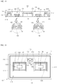
- FIG. 14 is a disassembled perspective view of a display apparatus not forming part of the claimed invention.
- the display apparatus 1000 may include a light guide plate 1041, a light emitting module 1031 supplying light to the light guide plate 1041, a reflective member 1022 under the light guide plate 1041, an optical sheet 1051 on the light guide plate 1041, a display panel 1061 on the optical sheet 1051, and a bottom cover 1011 receiving the light guide plate 1041, the light emitting module 1031, and the reflective member 1022, but the present disclosure is not limited thereto.
- the bottom cover 1011, the reflective member 1022, the light guide plate 1041, and the optical sheet 1051 may be defined as a light unit 1050.
- the light guide plate 1041 functions to transform linear light to planar light by diffusing the linear light.
- the light guide plate 1041 may be made of a transparent material, and may include one of acryl-series resin such as polymethyl metaacrylate (PMMA), polyethylene terephthlate (PET), poly carbonate (PC), COC, and polyethylene naphthalate resin.
- PMMA polymethyl metaacrylate
- PET polyethylene terephthlate
- PC poly carbonate
- COC polyethylene naphthalate resin
- the light emitting module 1031 provides light to at least a side surface of the light guide plate 1041, and finally acts as a light source of a display apparatus.
- the light emitting module 1031 may include at least one light emitting module in the bottom cover 1011, and provide light directly or indirectly from one side surface of the light guide plate 1041.
- the light emitting module 1031 may include a board 1033, and a light emitting device package 100 according to present inventions disclosed above, and the light emitting device packages 100 may be arranged apart by a predetermined interval from each other on the board 1033.
- the board 1033 may be a printed circuit board (PCB) including a circuit pattern (not shown).
- the board 1033 may include a metal core PCB (MCPCB), a flexible PCB (FPCB), etc. as well as the general PCB, but the present disclosure is not limited thereto.
- MCPCB metal core PCB
- FPCB flexible PCB
- the board 1033 may be removed.
- some of the radiant heat plate may contact an upper surface of the bottom cover 1011.
- the plurality of light emitting device packages 100 may be mounted on the board 1033 such that light emitting surfaces of the plurality of light emitting device packages 100 are spaced apart by a predetermined distance from the light guide plate 1041, but the present disclosure is not limited thereto.
- the light emitting device package 100 may supply light to a light incident part that is one side surface of the light guide plate 1041, directly or indirectly, but the present disclosure is not limited thereto.
- the reflective member 1022 may be provided under the light guide plate 1041.
- the reflective member 1022 reflects light incident from a lower surface of the light guide plate 1041 to allow the reflected light to be directed toward an upper direction, thereby capable of enhancing brightness of the light unit 1050.
- the reflective member 1022 may be formed of, for example, PET, PC, PVC resin, or the like, but the present disclosure is not limited thereto.
- the bottom cover 1011 may receive the light guide plate 1041, the light emitting module 1031, the reflective member 1022, and the like.
- the bottom cover 1011 may have a receiving part 1012 disposed in a box shape a top surface of which is opened, but the present disclosure is not limited thereto.
- the bottom cover 1011 may be coupled to a top cover, but the present disclosure is not limited thereto.
- the bottom cover 1011 may be disposed of a metal material or resin material, and may be manufactured by using a process such as a press molding or an injection molding. Also, the bottom cover 1011 may include metallic or nonmetallic material having a high thermal conductivity, but the present disclosure is not limited thereto.
- the display panel 1061 is, for example, an LCD panel, and includes first and second transparent substrates facing each other, and a liquid crystal layer interposed between the first and second substrates.
- a polarizing plate may be attached on at least one surface of the display panel 1061, but the present disclosure is not limited thereto.
- the display panel 1061 displays information by using light passing through the optical sheet 1051.
- the display apparatus 1000 may be applied to a variety of mobile terminals, monitors for notebook computers, monitors for lap-top computers, televisions, etc.
- the optical sheet 1051 is disposed between the display panel 1061 and the light guide plate 1041, and includes at least one transparent sheet.
- the optical sheet 1051 may include, for example, at least one of a diffusion sheet, a horizontal and/or vertical prism sheet, and a brightness reinforcing sheet.
- the diffusion sheet diffuses incident light
- the horizontal and/or vertical prism sheet focuses incident light on a display region
- the brightness reinforcing sheet enhances the brightness by reusing lost light.
- a protective sheet may be disposed on the display panel 1061, but the present disclosure is not limited thereto.
- the display apparatus 1000 may include the light guide plate 1041, and the optical sheet 1051 as optical members positioned on a light path of the light emitting module 1031, but the present disclosure is not limited thereto.
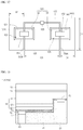
- FIG. 15 is a cross-sectional view of a display apparatus not forming part of the claimed invention.
- the display apparatus 1100 includes a bottom cover 1152, a board 1120 on which the light emitting device packages 100 disclosed above are arrayed, an optical member 1154, and a display panel 1155.
- the board 1120 and the light emitting device package 100 may be defined as a light emitting module 1160.
- the bottom cover 1152, the at least one light emitting module 1160, and the optical member 1154 may be defined as a light unit 1150.
- the bottom cover 1152 may be provided with a receiving part 1153, but the present disclosure is not limited thereto.
- the optical member 1154 may include at least one of a lens, a light guide plate, a diffusion sheet, a horizontal and vertical prism sheet, and a brightness reinforcing sheet.
- the light guide plate may be formed of polycarbonate (PC) or poly methyl methacrylate (PMMA), and may be removed.
- the diffusion sheet diffuses incident light
- the horizontal and vertical prism sheet focuses incident light on a display region
- the brightness reinforcing sheet enhances the brightness by reusing lost light.
- the optical member 1154 is disposed on the light emitting module 1160.
- the optical member 154 transforms light emitted from the light emitting module 1160 to planar light, and performs diffusion, light focusing, and the like.
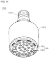
- FIG. 16 is a perspective view of a lighting unit not forming part of the claimed invention.
- the lighting unit 1500 may include a case 1510, a light emitting module 1530 including in the case 1510, and a connection terminal 1520 including in the case 1510 and supplied with an electric power from an external power supply.
- the case 1510 may be preferably formed of a material having good heat shielding characteristics, for example, a metal material or a resin material.
- the light emitting module 1530 may include a board 1532, and at least one light emitting device package 100 according to the present invention mounted on the board 1532.
- the light emitting device package 100 may include a plurality of light emitting device packages which are arrayed apart by a predetermined distance from one another in a matrix configuration.
- the board 1532 may be an insulator substrate on which a circuit pattern is printed, and may include, for example, a printed circuit board (PCB), a metal core PCB, a flexible PCB, a ceramic PCB, an FR-4 substrate, etc.
- PCB printed circuit board
- metal core PCB metal core PCB
- flexible PCB flexible PCB
- ceramic PCB ceramic PCB
- FR-4 substrate etc.
- the board 1532 may be formed of a material to efficiently reflect light, and a surface thereof may be formed in a color capable of efficiently reflecting light, for example, white color, or silver color.
- the at least one light emitting device packages 100 may be mounted on the board 1532.
- Each of the light emitting device packages 100 may include at least one light emitting diode (LED) chip.
- the LED chip may include a color LED emitting red, green, blue or white light, and a UV LED emitting ultraviolet (UV).
- the light emitting module 1530 may have a combination of various light emitting device packages so as to obtain desired color and luminance.
- the light emitting module 1530 may have a combination of a white LED, a red LED, and a green LED so as to obtain a high color rendering index (CRI).
- CRI color rendering index
- connection terminal 1520 may be electrically connected to the light emitting module 1530 to supply power.
- the connection terminal 1520 may be screwed and coupled to an external power in a socket type, but the present disclosure is not limited thereto.
- the connection terminal 1520 may be made in a pin type and inserted into an external power, or may be connected to the external power through a power line.
- the light extraction efficiency of the light emitting device package having a plurality of cavities can be improved.
- the reliability of the light emitting device package and the light unit having the same can be improved.
Claims (13)
- Lichtemittierende Vorrichtungsbaugruppe (100), die aufweist:einen ein Isoliermaterial aufweisenden Körper (110);eine erste Aussparung (125) in einem ersten Bereich des Körpers;eine zweite Aussparung (135) in einem zweiten Bereich des Körpers;einen ersten und einen zweiten Leitungsrahmen (121, 131), die voneinander beabstandet sind, in der ersten Aussparung;einen dritten Leitungsrahmen (141), der vom zweiten Leitungsrahmen (131) beabstandet ist, in der zweiten Aussparung;eine erste lichtemittierende Vorrichtung (151), die durch Flip-Verbindung mit dem ersten und dem zweiten Leitungsrahmen verbunden ist, in der ersten Aussparung;eine zweite lichtemittierende Vorrichtung (152), die durch Flip-Verbindung mit dem zweiten und dem dritten Leitungsrahmen verbunden ist, in der zweiten Aussparung; undein Formelement (161, 162) in der ersten und der zweiten Aussparung,wobei die erste und die zweite Aussparung (125, 135) in verschiedenen Bereichen im Körper (110) angeordnet sind und von einer oberen Fläche des Körpers (110) nach unten konkav sind,wobei ein erster Teil des zweiten Leitungsrahmens (131), der in der ersten Aussparung (125) angeordnet ist, mit einem zweiten Teil des zweiten Leitungsrahmens (131), der in der zweiten Aussparung (135) angeordnet ist, verbunden ist,dadurch gekennzeichnet, dass die Bodenflächen des ersten, zweiten und dritten Leitungsrahmens (121, 131, 141), die auf dem Boden der ersten und der zweiten Aussparung (125, 135) angeordnet sind, auf der gleichen horizontalen Ebene wie eine Bodenfläche des Körpers (110) angeordnet sind,wobei obere Teile (121A, 141A) des ersten und des dritten Leitungsrahmens (121, 141) nach außerhalb der ersten und der zweiten Aussparung (125, 135) gebogen sind und zwischen der oberen Fläche und der Bodenfläche des Körpers (110) näher an der oberen Fläche des Körpers (110) als an der Bodenfläche des Körpers (110) angeordnet sind,wobei die lichtemittierende Vorrichtungsbaugruppe (100) weiter aufweist:ein erstes Trennteil (126), das für eine Trennung zwischen dem ersten und dem zweiten Leitungsrahmen (121, 131) auf einer Bodenfläche und auf lateralen Seiten der ersten Aussparung (125) angeordnet ist; undein zweites Trennteil (136), das für eine Trennung zwischen dem zweiten und dem dritten Leitungsrahmen (131, 141) auf einer Bodenfläche und auf lateralen Seiten der zweiten Aussparung (135) angeordnet ist,wobei das erste und das zweite Trennteil (126, 136) aus einem Material des Körpers (110) gebildet sind.
- Lichtemittierende Vorrichtungsbaugruppe nach Anspruch 1, wobei sowohl die erste als auch die zweite lichtemittierende Vorrichtung (151, 152) aufweist:eine lichtemittierende Struktur (60); undeine erste und eine zweite Elektrode (75, 77) unter der lichtemittierenden Struktur,wobei die erste und die zweite Elektrode der ersten lichtemittierenden Vorrichtung (151) auf den ersten und den zweiten Leitungsrahmen (121, 131) gebondet sind unddie erste und die zweite Elektrode der zweiten lichtemittierenden Vorrichtung (152) auf den zweiten und den dritten Leitungsrahmen (131, 141) gebondet sind.
- Lichtemittierende Vorrichtungsbaugruppe nach Anspruch 2, wobei sowohl die erste als auch die zweite lichtemittierende Vorrichtung (151, 152) eine Halbleiterschicht oder ein Substrat (51) aufweist, die/das auf einer Oberseite der ersten und der zweiten lichtemittierenden Vorrichtung (151, 152) angeordnet ist.
- Lichtemittierende Vorrichtungsbaugruppe nach Anspruch 2 oder 3, wobei sowohl die erste als auch die zweite lichtemittierende Vorrichtung (151, 152) aufweist:eine reflektierende Elektrodenschicht (71), die zwischen der lichtemittierenden Struktur und der zweiten Elektrode angeordnet ist; undein isolierendes Trägerelement (91), das unter der reflektierenden Elektrodenschicht und um die erste und die zweite Elektrode herum angeordnet ist.
- Lichtemittierende Vorrichtungsbaugruppe nach einem der Ansprüche 1 bis 4, wobei der erste Leitungsrahmen (121), der in der ersten Aussparung (125) angeordnet ist, mit dem dritten Leitungsrahmen, der in der zweiten Aussparung (135) angeordnet ist, verbunden ist.
- Lichtemittierende Vorrichtungsbaugruppe nach einem der Ansprüche 1 bis 5, die ferner eine dritte Aussparung (145) aufweist, die auf dem Körper (110) angeordnet ist, wobei ein Verbindungsrahmen (130) des ersten Leitungsrahmens (121) und ein Verbindungsteil (133) des zweiten Leitungsrahmens (131) in der dritten Aussparung (145) angeordnet sind, und eine Schutzvorrichtung (153) auf dem Verbindungsrahmen (130) des ersten Leitungsrahmens (121) und dem Verbindungsteil (133) des zweiten Leitungsrahmens (131) in der dritten Aussparung (145) angeordnet ist.
- Lichtemittierende Vorrichtungsbaugruppe nach einem der Ansprüche 1 bis 6, wobei das Formelement (161, 162) bis zu einem oberen Bereich des Körpers (110) angeordnet ist.
- Lichtemittierende Vorrichtungsbaugruppe nach einem der Ansprüche 1 bis 7, die ferner aufweist:ein erstes Leitungsteil (121B), das von einer ersten lateralen Seite des Körpers (110) vom ersten Leitungsrahmen (121) nach unten vorsteht; undein zweites Leitungsteil (141B), das von einer zweiten lateralen Seite des Körpers (110) vom dritten Leitungsrahmen (131) nach unten vorsteht.
- Lichtemittierende Vorrichtungsbaugruppe nach einem der Ansprüche 1 bis 8, wobei eine Bodenfläche und laterale Seiten der ersten Aussparung (125) auf dem ersten und dem zweiten Leitungsrahmen (121, 131) angeordnet sind und eine Bodenfläche und laterale Seiten der zweiten Aussparung auf dem zweiten und dem dritten Leitungsrahmen (131, 141) angeordnet sind.
- Lichtemittierende Vorrichtungsbaugruppe nach einem der Ansprüche 1 bis 7, wobei ein erstes Ende des ersten Leitungsrahmens (121) und ein erstes Ende des zweiten Leitungsrahmens (131) eine Stufenstruktur aufweisen, die ein konkav-konvexes Muster hat, und das erste Trennteil (126) das konkav-konvexe Muster des ersten und des zweiten Leitungsrahmes (121, 131) berührt.
- Lichtemittierende Vorrichtungsbaugruppe nach Anspruch 10, wobei ein zweites Ende des zweiten Leitungsrahmens (131) und ein erstes Ende des dritten Leitungsrahmens (141) eine Stufenstruktur aufweisen, die ein konkav-konvexes Muster hat, und das zweite Trennteil (136) das konkav-konvexe Muster des zweiten und des dritten Leitungsrahmens (131, 141) berührt.
- Lichtemittierende Vorrichtungsbaugruppe nach einem der Ansprüche 8 bis 11, wobei die lateralen Seiten der ersten Aussparung (125) zur Bodenfläche der ersten Aussparung (125) geneigt sind.
- Beleuchtungssystem, das aufweist:mehrere lichtemittierende Vorrichtungsbaugruppen nach einem der Ansprüche 1 bis 12; undein Modulsubstrat (1033), wo die lichtemittierenden Vorrichtungsbaugruppen angeordnet sind.
Applications Claiming Priority (1)
| Application Number | Priority Date | Filing Date | Title |
|---|---|---|---|
| KR1020110076250A KR101871501B1 (ko) | 2011-07-29 | 2011-07-29 | 발광 소자 패키지 및 이를 구비한 조명 시스템 |
Publications (3)
| Publication Number | Publication Date |
|---|---|
| EP2551903A2 EP2551903A2 (de) | 2013-01-30 |
| EP2551903A3 EP2551903A3 (de) | 2015-04-22 |
| EP2551903B1 true EP2551903B1 (de) | 2020-12-16 |
Family
ID=45833226
Family Applications (1)
| Application Number | Title | Priority Date | Filing Date |
|---|---|---|---|
| EP12160393.0A Active EP2551903B1 (de) | 2011-07-29 | 2012-03-20 | Gehäuse für lichtemittierende Vorrichtung und Beleuchtungssystem damit |
Country Status (5)
| Country | Link |
|---|---|
| US (2) | US8772794B2 (de) |
| EP (1) | EP2551903B1 (de) |
| JP (1) | JP6101001B2 (de) |
| KR (1) | KR101871501B1 (de) |
| CN (1) | CN102903837B (de) |
Families Citing this family (45)
| Publication number | Priority date | Publication date | Assignee | Title |
|---|---|---|---|---|
| KR20130098048A (ko) * | 2012-02-27 | 2013-09-04 | 엘지이노텍 주식회사 | 발광소자 패키지 |
| WO2014184698A1 (en) * | 2013-05-14 | 2014-11-20 | Koninklijke Philips N.V. | Chip scale light emitting device package in molded leadframe |
| CN103296188B (zh) * | 2013-05-27 | 2015-12-09 | 北京半导体照明科技促进中心 | Led封装结构及其制作方法 |
| CN104251417A (zh) * | 2013-06-28 | 2014-12-31 | 展晶科技(深圳)有限公司 | 光源模组 |
| DE102013213073A1 (de) * | 2013-07-04 | 2015-01-08 | Osram Opto Semiconductors Gmbh | Verfahren zum Herstellen eines optoelektronischen Bauelementes |
| JP2015041685A (ja) * | 2013-08-21 | 2015-03-02 | 豊田合成株式会社 | 発光装置 |
| TW201517323A (zh) * | 2013-08-27 | 2015-05-01 | Glo Ab | 模製發光二極體封裝及其製造方法 |
| KR20150025231A (ko) * | 2013-08-28 | 2015-03-10 | 서울반도체 주식회사 | 광원 모듈 및 그 제조 방법, 및 백라이트 유닛 |
| US9847462B2 (en) * | 2013-10-29 | 2017-12-19 | Point Engineering Co., Ltd. | Array substrate for mounting chip and method for manufacturing the same |
| WO2015104604A1 (en) | 2014-01-08 | 2015-07-16 | Koninklijke Philips N.V. | Wavelength converted semiconductor light emitting device |
| JP2015220204A (ja) * | 2014-05-21 | 2015-12-07 | ソニー株式会社 | 照明装置および表示装置 |
| DE102014108295A1 (de) * | 2014-06-12 | 2015-12-17 | Osram Opto Semiconductors Gmbh | Licht emittierendes Halbleiterbauelement |
| KR102222580B1 (ko) | 2014-07-30 | 2021-03-05 | 삼성전자주식회사 | 발광 소자 패키지 및 이를 포함하는 표시 장치 |
| USD757665S1 (en) * | 2014-09-30 | 2016-05-31 | Lite-On Opto Technology (Changzhou) Co., Ltd. | Light emitting diode |
| USD750578S1 (en) * | 2014-09-30 | 2016-03-01 | Lite-On Opto Technology (Changzhou) Co., Ltd. | Light emitting diode |
| USD750579S1 (en) * | 2014-09-30 | 2016-03-01 | Lite-On Opto Technology (Changzhou) Co., Ltd. | Light emitting diode |
| USD757664S1 (en) * | 2014-09-30 | 2016-05-31 | Lite-On Opto Technology (Changzhou) Co., Ltd. | Light emitting diode |
| KR102306802B1 (ko) * | 2014-11-18 | 2021-09-30 | 서울반도체 주식회사 | 발광 장치 |
| KR102288384B1 (ko) * | 2014-11-18 | 2021-08-11 | 서울반도체 주식회사 | 발광 장치 |
| KR101672781B1 (ko) | 2014-11-18 | 2016-11-07 | 피에스아이 주식회사 | 수평배열 어셈블리용 초소형 led 소자, 이의 제조방법 및 이를 포함하는 수평배열 어셈블리 |
| CN111490146A (zh) | 2014-11-18 | 2020-08-04 | 首尔半导体株式会社 | 发光装置 |
| KR101713818B1 (ko) | 2014-11-18 | 2017-03-10 | 피에스아이 주식회사 | 초소형 led 소자를 포함하는 전극어셈블리 및 그 제조방법 |
| JP6206442B2 (ja) * | 2015-04-30 | 2017-10-04 | 日亜化学工業株式会社 | パッケージ及びその製造方法、並びに発光装置 |
| US10101016B2 (en) * | 2015-06-08 | 2018-10-16 | Epistar Corporation | Lighting apparatus |
| US10008648B2 (en) | 2015-10-08 | 2018-06-26 | Semicon Light Co., Ltd. | Semiconductor light emitting device |
| KR20170058489A (ko) * | 2015-11-18 | 2017-05-29 | 주식회사 세미콘라이트 | 반도체 발광소자용 프레임 |
| KR101730977B1 (ko) | 2016-01-14 | 2017-04-28 | 피에스아이 주식회사 | 초소형 led 전극어셈블리 |
| CN105702670A (zh) * | 2016-04-06 | 2016-06-22 | 深圳市九洲光电科技有限公司 | 一种透镜式smd封装器件 |
| KR20180007025A (ko) * | 2016-07-11 | 2018-01-22 | 삼성디스플레이 주식회사 | 초소형 발광 소자를 포함하는 픽셀 구조체, 표시장치 및 그 제조방법 |
| KR102608419B1 (ko) * | 2016-07-12 | 2023-12-01 | 삼성디스플레이 주식회사 | 표시장치 및 표시장치의 제조방법 |
| CN106782128A (zh) * | 2017-01-24 | 2017-05-31 | 深圳市华星光电技术有限公司 | 微发光二极管显示面板及其制造方法 |
| US11677059B2 (en) | 2017-04-26 | 2023-06-13 | Samsung Electronics Co., Ltd. | Light-emitting device package including a lead frame |
| KR102335216B1 (ko) * | 2017-04-26 | 2021-12-03 | 삼성전자 주식회사 | 발광소자 패키지 |
| JP2018190849A (ja) * | 2017-05-09 | 2018-11-29 | スタンレー電気株式会社 | 発光装置 |
| TWI820026B (zh) | 2017-06-21 | 2023-11-01 | 荷蘭商露明控股公司 | 具有改善的熱行為的照明組件 |
| KR102441566B1 (ko) * | 2017-08-07 | 2022-09-07 | 삼성디스플레이 주식회사 | 발광 장치 및 발광 장치의 제조 방법 |
| KR102513267B1 (ko) | 2017-10-13 | 2023-03-23 | 삼성디스플레이 주식회사 | 표시 장치 및 이의 제조 방법 |
| KR102131231B1 (ko) * | 2018-02-08 | 2020-07-07 | 우리이앤엘 주식회사 | 반도체 발광소자 및 이를 이용한 백라이트 |
| TWI700786B (zh) * | 2018-03-28 | 2020-08-01 | 南茂科技股份有限公司 | 薄膜覆晶封裝結構 |
| TWI778071B (zh) * | 2018-06-01 | 2022-09-21 | 聯華電子股份有限公司 | 半導體裝置 |
| KR102103461B1 (ko) * | 2018-06-26 | 2020-04-23 | 알에프에이치아이씨 주식회사 | Rf 트랜지스터 패키지 및 이의 제조방법 |
| US10916690B2 (en) * | 2018-11-28 | 2021-02-09 | International Business Machines Corporation | Electrical leads for trenched qubits |
| KR102535276B1 (ko) * | 2018-12-20 | 2023-05-23 | 삼성디스플레이 주식회사 | 표시 장치 및 그의 제조 방법 |
| KR20210104392A (ko) * | 2020-02-17 | 2021-08-25 | 삼성디스플레이 주식회사 | 표시 장치 |
| US20230387356A1 (en) * | 2022-05-31 | 2023-11-30 | Creeled, Inc. | Light-emitting diode packages with lead frame structures for flip-chip mounting of light-emitting diode chips |
Citations (1)
| Publication number | Priority date | Publication date | Assignee | Title |
|---|---|---|---|---|
| KR101051065B1 (ko) * | 2010-03-10 | 2011-07-21 | 일진반도체 주식회사 | 발광다이오드 패키지 |
Family Cites Families (24)
| Publication number | Priority date | Publication date | Assignee | Title |
|---|---|---|---|---|
| JPS6335089A (ja) | 1986-07-30 | 1988-02-15 | Nippon Hoso Kyokai <Nhk> | 非直線エンフアシス方式 |
| JPH0447747Y2 (de) * | 1986-08-25 | 1992-11-11 | ||
| JPH07110927B2 (ja) | 1990-07-04 | 1995-11-29 | 岩手県 | ポリアミド系樹脂組成物のめっき方法 |
| JPH0465463U (de) * | 1990-10-19 | 1992-06-08 | ||
| JP3189703B2 (ja) * | 1996-10-08 | 2001-07-16 | 富士通株式会社 | 半導体装置及びその製造方法 |
| DE19638667C2 (de) * | 1996-09-20 | 2001-05-17 | Osram Opto Semiconductors Gmbh | Mischfarbiges Licht abstrahlendes Halbleiterbauelement mit Lumineszenzkonversionselement |
| DE10041686A1 (de) * | 2000-08-24 | 2002-03-14 | Osram Opto Semiconductors Gmbh | Bauelement mit einer Vielzahl von Lumineszenzdiodenchips |
| US6531328B1 (en) * | 2001-10-11 | 2003-03-11 | Solidlite Corporation | Packaging of light-emitting diode |
| WO2004107443A1 (de) * | 2003-06-03 | 2004-12-09 | Asetronics Ag | Isoliertes metallsubstrat mit wenigstens einer leuchtdiode, leuchtdiodenmatrix und herstellungsverfahren |
| CN100459189C (zh) * | 2003-11-19 | 2009-02-04 | 日亚化学工业株式会社 | 半导体元件 |
| JP2006222271A (ja) * | 2005-02-10 | 2006-08-24 | Ngk Spark Plug Co Ltd | 発光素子実装用基板 |
| JP2007214474A (ja) * | 2006-02-13 | 2007-08-23 | Matsushita Electric Ind Co Ltd | エッジライトとその製造方法 |
| JP4905069B2 (ja) * | 2006-11-09 | 2012-03-28 | 豊田合成株式会社 | 発光装置及びその製造方法 |
| TWM318795U (en) * | 2006-12-18 | 2007-09-11 | Lighthouse Technology Co Ltd | Package structure |
| JP2008270305A (ja) * | 2007-04-17 | 2008-11-06 | Nichia Corp | 発光装置 |
| TWM342455U (en) * | 2007-11-14 | 2008-10-11 | Taiwan Green Energy Co Ltd | LED lighting device embedded in ceiling |
| US8089140B2 (en) * | 2008-09-25 | 2012-01-03 | Silitek Electronic (Guangzhou) Co., Ltd. | Lead frame assembly, lead frame and insulating housing combination, and led module having the same |
| KR100982994B1 (ko) * | 2008-10-15 | 2010-09-17 | 삼성엘이디 주식회사 | Led 패키지 모듈 |
| JP4724222B2 (ja) | 2008-12-12 | 2011-07-13 | 株式会社東芝 | 発光装置の製造方法 |
| TWI380433B (en) * | 2009-02-25 | 2012-12-21 | Everlight Electronics Co Ltd | Light emitting diode package |
| WO2010140693A1 (ja) * | 2009-06-04 | 2010-12-09 | 三洋電機株式会社 | 電子部品 |
| JP5471244B2 (ja) * | 2009-09-29 | 2014-04-16 | 豊田合成株式会社 | 照明装置 |
| KR101039994B1 (ko) * | 2010-05-24 | 2011-06-09 | 엘지이노텍 주식회사 | 발광소자 및 이를 구비한 라이트 유닛 |
| KR101103674B1 (ko) * | 2010-06-01 | 2012-01-11 | 엘지이노텍 주식회사 | 발광 소자 |
-
2011
- 2011-07-29 KR KR1020110076250A patent/KR101871501B1/ko active IP Right Grant
- 2011-12-14 US US13/325,326 patent/US8772794B2/en active Active
-
2012
- 2012-03-09 JP JP2012053425A patent/JP6101001B2/ja active Active
- 2012-03-14 CN CN201210067596.8A patent/CN102903837B/zh active Active
- 2012-03-20 EP EP12160393.0A patent/EP2551903B1/de active Active
-
2014
- 2014-01-15 US US14/155,519 patent/US9882104B2/en active Active
Patent Citations (1)
| Publication number | Priority date | Publication date | Assignee | Title |
|---|---|---|---|---|
| KR101051065B1 (ko) * | 2010-03-10 | 2011-07-21 | 일진반도체 주식회사 | 발광다이오드 패키지 |
Also Published As
| Publication number | Publication date |
|---|---|
| KR101871501B1 (ko) | 2018-06-27 |
| US8772794B2 (en) | 2014-07-08 |
| CN102903837A (zh) | 2013-01-30 |
| US20130062632A1 (en) | 2013-03-14 |
| EP2551903A3 (de) | 2015-04-22 |
| JP2013033905A (ja) | 2013-02-14 |
| JP6101001B2 (ja) | 2017-03-22 |
| US20140124801A1 (en) | 2014-05-08 |
| CN102903837B (zh) | 2016-12-14 |
| KR20130014254A (ko) | 2013-02-07 |
| EP2551903A2 (de) | 2013-01-30 |
| US9882104B2 (en) | 2018-01-30 |
Similar Documents
| Publication | Publication Date | Title |
|---|---|---|
| EP2551903B1 (de) | Gehäuse für lichtemittierende Vorrichtung und Beleuchtungssystem damit | |
| US10559734B2 (en) | Light emitting device package and light unit including the same | |
| US9520383B2 (en) | Light emitting device package and lighting system | |
| EP2897182B1 (de) | Lichtemittierende Vorrichtung | |
| US8319241B2 (en) | Light emitting device, light emitting device package, and lighting system | |
| KR101998765B1 (ko) | 발광소자 패키지 | |
| US8624270B2 (en) | Device having a plurality of light emitting structures bonded by adhesive layers and light emitting device package having the same | |
| KR101979942B1 (ko) | 발광 소자 패키지 및 이를 구비한 조명 시스템 | |
| EP2355188A2 (de) | Lichtemittierende Vorrichtung und Gehäuse mit lichtemittierender Vorrichtung | |
| KR20120132211A (ko) | 발광소자, 발광 모듈 및 발광 소자 제조방법 | |
| KR101900269B1 (ko) | 발광 소자 및 이를 구비한 발광 장치 | |
| KR101896683B1 (ko) | 발광 모듈 및 이를 구비한 조명 시스템 | |
| KR101901839B1 (ko) | 발광소자, 발광 소자 패키지 및 발광 모듈 |
Legal Events
| Date | Code | Title | Description |
|---|---|---|---|
| PUAI | Public reference made under article 153(3) epc to a published international application that has entered the european phase |
Free format text: ORIGINAL CODE: 0009012 |
|
| AK | Designated contracting states |
Kind code of ref document: A2 Designated state(s): AL AT BE BG CH CY CZ DE DK EE ES FI FR GB GR HR HU IE IS IT LI LT LU LV MC MK MT NL NO PL PT RO RS SE SI SK SM TR |
|
| AX | Request for extension of the european patent |
Extension state: BA ME |
|
| 17P | Request for examination filed |
Effective date: 20140328 |
|
| RBV | Designated contracting states (corrected) |
Designated state(s): AL AT BE BG CH CY CZ DE DK EE ES FI FR GB GR HR HU IE IS IT LI LT LU LV MC MK MT NL NO PL PT RO RS SE SI SK SM TR |
|
| RAP1 | Party data changed (applicant data changed or rights of an application transferred) |
Owner name: LG INNOTEK CO., LTD. |
|
| PUAL | Search report despatched |
Free format text: ORIGINAL CODE: 0009013 |
|
| AK | Designated contracting states |
Kind code of ref document: A3 Designated state(s): AL AT BE BG CH CY CZ DE DK EE ES FI FR GB GR HR HU IE IS IT LI LT LU LV MC MK MT NL NO PL PT RO RS SE SI SK SM TR |
|
| AX | Request for extension of the european patent |
Extension state: BA ME |
|
| RIC1 | Information provided on ipc code assigned before grant |
Ipc: H01L 25/075 20060101AFI20150319BHEP Ipc: H01L 33/60 20100101ALN20150319BHEP Ipc: H01L 33/48 20100101ALI20150319BHEP Ipc: H01L 33/46 20100101ALN20150319BHEP Ipc: H01L 33/40 20100101ALN20150319BHEP Ipc: H01L 25/16 20060101ALN20150319BHEP Ipc: H01L 33/62 20100101ALI20150319BHEP |
|
| RAP1 | Party data changed (applicant data changed or rights of an application transferred) |
Owner name: LG INNOTEK CO., LTD. |
|
| STAA | Information on the status of an ep patent application or granted ep patent |
Free format text: STATUS: EXAMINATION IS IN PROGRESS |
|
| 17Q | First examination report despatched |
Effective date: 20191127 |
|
| RIC1 | Information provided on ipc code assigned before grant |
Ipc: F21Y 105/10 20160101ALN20200421BHEP Ipc: H01L 25/075 20060101AFI20200421BHEP Ipc: H01L 33/46 20100101ALN20200421BHEP Ipc: H01L 33/40 20100101ALN20200421BHEP Ipc: H01L 33/48 20100101ALI20200421BHEP Ipc: F21Y 115/10 20160101ALN20200421BHEP Ipc: H01L 33/60 20100101ALN20200421BHEP Ipc: H01L 25/16 20060101ALN20200421BHEP Ipc: H01L 33/64 20100101ALI20200421BHEP Ipc: H01L 33/62 20100101ALI20200421BHEP |
|
| GRAP | Despatch of communication of intention to grant a patent |
Free format text: ORIGINAL CODE: EPIDOSNIGR1 |
|
| STAA | Information on the status of an ep patent application or granted ep patent |
Free format text: STATUS: GRANT OF PATENT IS INTENDED |
|
| RIC1 | Information provided on ipc code assigned before grant |
Ipc: H01L 33/60 20100101ALN20200512BHEP Ipc: H01L 33/48 20100101ALI20200512BHEP Ipc: H01L 25/075 20060101AFI20200512BHEP Ipc: F21Y 115/10 20160101ALN20200512BHEP Ipc: H01L 25/16 20060101ALN20200512BHEP Ipc: H01L 33/64 20100101ALI20200512BHEP Ipc: H01L 33/40 20100101ALN20200512BHEP Ipc: H01L 33/62 20100101ALI20200512BHEP Ipc: H01L 33/46 20100101ALN20200512BHEP Ipc: F21Y 105/10 20160101ALN20200512BHEP |
|
| INTG | Intention to grant announced |
Effective date: 20200605 |
|
| GRAJ | Information related to disapproval of communication of intention to grant by the applicant or resumption of examination proceedings by the epo deleted |
Free format text: ORIGINAL CODE: EPIDOSDIGR1 |
|
| STAA | Information on the status of an ep patent application or granted ep patent |
Free format text: STATUS: EXAMINATION IS IN PROGRESS |
|
| INTC | Intention to grant announced (deleted) | ||
| GRAP | Despatch of communication of intention to grant a patent |
Free format text: ORIGINAL CODE: EPIDOSNIGR1 |
|
| STAA | Information on the status of an ep patent application or granted ep patent |
Free format text: STATUS: GRANT OF PATENT IS INTENDED |
|
| RIC1 | Information provided on ipc code assigned before grant |
Ipc: H01L 25/16 20060101ALN20200821BHEP Ipc: H01L 33/62 20100101ALI20200821BHEP Ipc: H01L 33/64 20100101ALI20200821BHEP Ipc: H01L 33/60 20100101ALN20200821BHEP Ipc: H01L 25/075 20060101AFI20200821BHEP Ipc: H01L 33/46 20100101ALN20200821BHEP Ipc: F21Y 115/10 20160101ALN20200821BHEP Ipc: F21Y 105/10 20160101ALN20200821BHEP Ipc: H01L 33/48 20100101ALI20200821BHEP Ipc: H01L 33/40 20100101ALN20200821BHEP |
|
| RIC1 | Information provided on ipc code assigned before grant |
Ipc: F21Y 105/10 20160101ALN20200908BHEP Ipc: H01L 33/46 20100101ALN20200908BHEP Ipc: H01L 33/60 20100101ALN20200908BHEP Ipc: H01L 25/075 20060101AFI20200908BHEP Ipc: F21Y 115/10 20160101ALN20200908BHEP Ipc: H01L 33/48 20100101ALI20200908BHEP Ipc: H01L 33/40 20100101ALN20200908BHEP Ipc: H01L 33/64 20100101ALI20200908BHEP Ipc: H01L 25/16 20060101ALN20200908BHEP Ipc: H01L 33/62 20100101ALI20200908BHEP |
|
| INTG | Intention to grant announced |
Effective date: 20200925 |
|
| GRAS | Grant fee paid |
Free format text: ORIGINAL CODE: EPIDOSNIGR3 |
|
| GRAA | (expected) grant |
Free format text: ORIGINAL CODE: 0009210 |
|
| STAA | Information on the status of an ep patent application or granted ep patent |
Free format text: STATUS: THE PATENT HAS BEEN GRANTED |
|
| AK | Designated contracting states |
Kind code of ref document: B1 Designated state(s): AL AT BE BG CH CY CZ DE DK EE ES FI FR GB GR HR HU IE IS IT LI LT LU LV MC MK MT NL NO PL PT RO RS SE SI SK SM TR |
|
| REG | Reference to a national code |
Ref country code: GB Ref legal event code: FG4D |
|
| REG | Reference to a national code |
Ref country code: IE Ref legal event code: FG4D |
|
| REG | Reference to a national code |
Ref country code: DE Ref legal event code: R096 Ref document number: 602012073717 Country of ref document: DE |
|
| REG | Reference to a national code |
Ref country code: AT Ref legal event code: REF Ref document number: 1346356 Country of ref document: AT Kind code of ref document: T Effective date: 20210115 |
|
| PG25 | Lapsed in a contracting state [announced via postgrant information from national office to epo] |
Ref country code: NO Free format text: LAPSE BECAUSE OF FAILURE TO SUBMIT A TRANSLATION OF THE DESCRIPTION OR TO PAY THE FEE WITHIN THE PRESCRIBED TIME-LIMIT Effective date: 20210316 Ref country code: FI Free format text: LAPSE BECAUSE OF FAILURE TO SUBMIT A TRANSLATION OF THE DESCRIPTION OR TO PAY THE FEE WITHIN THE PRESCRIBED TIME-LIMIT Effective date: 20201216 Ref country code: RS Free format text: LAPSE BECAUSE OF FAILURE TO SUBMIT A TRANSLATION OF THE DESCRIPTION OR TO PAY THE FEE WITHIN THE PRESCRIBED TIME-LIMIT Effective date: 20201216 Ref country code: GR Free format text: LAPSE BECAUSE OF FAILURE TO SUBMIT A TRANSLATION OF THE DESCRIPTION OR TO PAY THE FEE WITHIN THE PRESCRIBED TIME-LIMIT Effective date: 20210317 |
|
| REG | Reference to a national code |
Ref country code: AT Ref legal event code: MK05 Ref document number: 1346356 Country of ref document: AT Kind code of ref document: T Effective date: 20201216 |
|
| REG | Reference to a national code |
Ref country code: NL Ref legal event code: MP Effective date: 20201216 |
|
| PG25 | Lapsed in a contracting state [announced via postgrant information from national office to epo] |
Ref country code: LV Free format text: LAPSE BECAUSE OF FAILURE TO SUBMIT A TRANSLATION OF THE DESCRIPTION OR TO PAY THE FEE WITHIN THE PRESCRIBED TIME-LIMIT Effective date: 20201216 Ref country code: SE Free format text: LAPSE BECAUSE OF FAILURE TO SUBMIT A TRANSLATION OF THE DESCRIPTION OR TO PAY THE FEE WITHIN THE PRESCRIBED TIME-LIMIT Effective date: 20201216 Ref country code: BG Free format text: LAPSE BECAUSE OF FAILURE TO SUBMIT A TRANSLATION OF THE DESCRIPTION OR TO PAY THE FEE WITHIN THE PRESCRIBED TIME-LIMIT Effective date: 20210316 |
|
| PG25 | Lapsed in a contracting state [announced via postgrant information from national office to epo] |
Ref country code: HR Free format text: LAPSE BECAUSE OF FAILURE TO SUBMIT A TRANSLATION OF THE DESCRIPTION OR TO PAY THE FEE WITHIN THE PRESCRIBED TIME-LIMIT Effective date: 20201216 Ref country code: NL Free format text: LAPSE BECAUSE OF FAILURE TO SUBMIT A TRANSLATION OF THE DESCRIPTION OR TO PAY THE FEE WITHIN THE PRESCRIBED TIME-LIMIT Effective date: 20201216 |
|
| REG | Reference to a national code |
Ref country code: LT Ref legal event code: MG9D |
|
| PG25 | Lapsed in a contracting state [announced via postgrant information from national office to epo] |
Ref country code: CZ Free format text: LAPSE BECAUSE OF FAILURE TO SUBMIT A TRANSLATION OF THE DESCRIPTION OR TO PAY THE FEE WITHIN THE PRESCRIBED TIME-LIMIT Effective date: 20201216 Ref country code: EE Free format text: LAPSE BECAUSE OF FAILURE TO SUBMIT A TRANSLATION OF THE DESCRIPTION OR TO PAY THE FEE WITHIN THE PRESCRIBED TIME-LIMIT Effective date: 20201216 Ref country code: SM Free format text: LAPSE BECAUSE OF FAILURE TO SUBMIT A TRANSLATION OF THE DESCRIPTION OR TO PAY THE FEE WITHIN THE PRESCRIBED TIME-LIMIT Effective date: 20201216 Ref country code: PT Free format text: LAPSE BECAUSE OF FAILURE TO SUBMIT A TRANSLATION OF THE DESCRIPTION OR TO PAY THE FEE WITHIN THE PRESCRIBED TIME-LIMIT Effective date: 20210416 Ref country code: RO Free format text: LAPSE BECAUSE OF FAILURE TO SUBMIT A TRANSLATION OF THE DESCRIPTION OR TO PAY THE FEE WITHIN THE PRESCRIBED TIME-LIMIT Effective date: 20201216 Ref country code: SK Free format text: LAPSE BECAUSE OF FAILURE TO SUBMIT A TRANSLATION OF THE DESCRIPTION OR TO PAY THE FEE WITHIN THE PRESCRIBED TIME-LIMIT Effective date: 20201216 Ref country code: LT Free format text: LAPSE BECAUSE OF FAILURE TO SUBMIT A TRANSLATION OF THE DESCRIPTION OR TO PAY THE FEE WITHIN THE PRESCRIBED TIME-LIMIT Effective date: 20201216 |
|
| RAP2 | Party data changed (patent owner data changed or rights of a patent transferred) |
Owner name: SUZHOU LEKIN SEMICONDUCTOR CO., LTD. |
|
| PG25 | Lapsed in a contracting state [announced via postgrant information from national office to epo] |
Ref country code: PL Free format text: LAPSE BECAUSE OF FAILURE TO SUBMIT A TRANSLATION OF THE DESCRIPTION OR TO PAY THE FEE WITHIN THE PRESCRIBED TIME-LIMIT Effective date: 20201216 Ref country code: AT Free format text: LAPSE BECAUSE OF FAILURE TO SUBMIT A TRANSLATION OF THE DESCRIPTION OR TO PAY THE FEE WITHIN THE PRESCRIBED TIME-LIMIT Effective date: 20201216 |
|
| REG | Reference to a national code |
Ref country code: DE Ref legal event code: R097 Ref document number: 602012073717 Country of ref document: DE |
|
| REG | Reference to a national code |
Ref country code: DE Ref legal event code: R081 Ref document number: 602012073717 Country of ref document: DE Owner name: SUZHOU LEKIN SEMICONDUCTOR CO. LTD., TAICANG, CN Free format text: FORMER OWNER: LG INNOTEK CO., LTD., SEOUL, KR |
|
| PG25 | Lapsed in a contracting state [announced via postgrant information from national office to epo] |
Ref country code: IS Free format text: LAPSE BECAUSE OF FAILURE TO SUBMIT A TRANSLATION OF THE DESCRIPTION OR TO PAY THE FEE WITHIN THE PRESCRIBED TIME-LIMIT Effective date: 20210416 |
|
| PLBE | No opposition filed within time limit |
Free format text: ORIGINAL CODE: 0009261 |
|
| STAA | Information on the status of an ep patent application or granted ep patent |
Free format text: STATUS: NO OPPOSITION FILED WITHIN TIME LIMIT |
|
| PG25 | Lapsed in a contracting state [announced via postgrant information from national office to epo] |
Ref country code: IT Free format text: LAPSE BECAUSE OF FAILURE TO SUBMIT A TRANSLATION OF THE DESCRIPTION OR TO PAY THE FEE WITHIN THE PRESCRIBED TIME-LIMIT Effective date: 20201216 Ref country code: AL Free format text: LAPSE BECAUSE OF FAILURE TO SUBMIT A TRANSLATION OF THE DESCRIPTION OR TO PAY THE FEE WITHIN THE PRESCRIBED TIME-LIMIT Effective date: 20201216 Ref country code: MC Free format text: LAPSE BECAUSE OF FAILURE TO SUBMIT A TRANSLATION OF THE DESCRIPTION OR TO PAY THE FEE WITHIN THE PRESCRIBED TIME-LIMIT Effective date: 20201216 |
|
| REG | Reference to a national code |
Ref country code: CH Ref legal event code: PL |
|
| 26N | No opposition filed |
Effective date: 20210917 |
|
| GBPC | Gb: european patent ceased through non-payment of renewal fee |
Effective date: 20210320 |
|
| PG25 | Lapsed in a contracting state [announced via postgrant information from national office to epo] |
Ref country code: ES Free format text: LAPSE BECAUSE OF FAILURE TO SUBMIT A TRANSLATION OF THE DESCRIPTION OR TO PAY THE FEE WITHIN THE PRESCRIBED TIME-LIMIT Effective date: 20201216 Ref country code: DK Free format text: LAPSE BECAUSE OF FAILURE TO SUBMIT A TRANSLATION OF THE DESCRIPTION OR TO PAY THE FEE WITHIN THE PRESCRIBED TIME-LIMIT Effective date: 20201216 |
|
| REG | Reference to a national code |
Ref country code: BE Ref legal event code: MM Effective date: 20210331 |
|
| PG25 | Lapsed in a contracting state [announced via postgrant information from national office to epo] |
Ref country code: CH Free format text: LAPSE BECAUSE OF NON-PAYMENT OF DUE FEES Effective date: 20210331 Ref country code: LU Free format text: LAPSE BECAUSE OF NON-PAYMENT OF DUE FEES Effective date: 20210320 Ref country code: LI Free format text: LAPSE BECAUSE OF NON-PAYMENT OF DUE FEES Effective date: 20210331 Ref country code: GB Free format text: LAPSE BECAUSE OF NON-PAYMENT OF DUE FEES Effective date: 20210320 Ref country code: FR Free format text: LAPSE BECAUSE OF NON-PAYMENT OF DUE FEES Effective date: 20210331 Ref country code: IE Free format text: LAPSE BECAUSE OF NON-PAYMENT OF DUE FEES Effective date: 20210320 |
|
| PG25 | Lapsed in a contracting state [announced via postgrant information from national office to epo] |
Ref country code: SI Free format text: LAPSE BECAUSE OF FAILURE TO SUBMIT A TRANSLATION OF THE DESCRIPTION OR TO PAY THE FEE WITHIN THE PRESCRIBED TIME-LIMIT Effective date: 20201216 |
|
| PG25 | Lapsed in a contracting state [announced via postgrant information from national office to epo] |
Ref country code: IS Free format text: LAPSE BECAUSE OF FAILURE TO SUBMIT A TRANSLATION OF THE DESCRIPTION OR TO PAY THE FEE WITHIN THE PRESCRIBED TIME-LIMIT Effective date: 20210416 |
|
| PG25 | Lapsed in a contracting state [announced via postgrant information from national office to epo] |
Ref country code: BE Free format text: LAPSE BECAUSE OF NON-PAYMENT OF DUE FEES Effective date: 20210331 |
|
| PG25 | Lapsed in a contracting state [announced via postgrant information from national office to epo] |
Ref country code: HU Free format text: LAPSE BECAUSE OF FAILURE TO SUBMIT A TRANSLATION OF THE DESCRIPTION OR TO PAY THE FEE WITHIN THE PRESCRIBED TIME-LIMIT; INVALID AB INITIO Effective date: 20120320 Ref country code: CY Free format text: LAPSE BECAUSE OF FAILURE TO SUBMIT A TRANSLATION OF THE DESCRIPTION OR TO PAY THE FEE WITHIN THE PRESCRIBED TIME-LIMIT Effective date: 20201216 |
|
| PGFP | Annual fee paid to national office [announced via postgrant information from national office to epo] |
Ref country code: DE Payment date: 20230214 Year of fee payment: 12 |