EP2539934B1 - High holding voltage device - Google Patents
High holding voltage device Download PDFInfo
- Publication number
- EP2539934B1 EP2539934B1 EP11704784.5A EP11704784A EP2539934B1 EP 2539934 B1 EP2539934 B1 EP 2539934B1 EP 11704784 A EP11704784 A EP 11704784A EP 2539934 B1 EP2539934 B1 EP 2539934B1
- Authority
- EP
- European Patent Office
- Prior art keywords
- highly
- doped region
- doped
- lowly
- region
- Prior art date
- Legal status (The legal status is an assumption and is not a legal conclusion. Google has not performed a legal analysis and makes no representation as to the accuracy of the status listed.)
- Active
Links
- 239000004065 semiconductor Substances 0.000 claims description 9
- 239000002184 metal Substances 0.000 claims description 8
- XUIMIQQOPSSXEZ-UHFFFAOYSA-N Silicon Chemical compound [Si] XUIMIQQOPSSXEZ-UHFFFAOYSA-N 0.000 claims description 6
- 229910052710 silicon Inorganic materials 0.000 claims description 6
- 239000010703 silicon Substances 0.000 claims description 6
- 239000003990 capacitor Substances 0.000 claims description 5
- 229910044991 metal oxide Inorganic materials 0.000 claims description 5
- 150000004706 metal oxides Chemical class 0.000 claims description 5
- 239000002019 doping agent Substances 0.000 claims 4
- 238000002955 isolation Methods 0.000 description 12
- 239000000969 carrier Substances 0.000 description 8
- 230000000694 effects Effects 0.000 description 6
- 230000015556 catabolic process Effects 0.000 description 5
- 230000001172 regenerating effect Effects 0.000 description 5
- 230000015572 biosynthetic process Effects 0.000 description 3
- 230000008713 feedback mechanism Effects 0.000 description 3
- 238000002347 injection Methods 0.000 description 3
- 239000007924 injection Substances 0.000 description 3
- 230000007423 decrease Effects 0.000 description 2
- 230000003247 decreasing effect Effects 0.000 description 2
- 230000014509 gene expression Effects 0.000 description 2
- 230000001960 triggered effect Effects 0.000 description 2
- 102000004129 N-Type Calcium Channels Human genes 0.000 description 1
- 108090000699 N-Type Calcium Channels Proteins 0.000 description 1
- 230000000295 complement effect Effects 0.000 description 1
- 230000001419 dependent effect Effects 0.000 description 1
- 230000003503 early effect Effects 0.000 description 1
- 238000005516 engineering process Methods 0.000 description 1
- 239000000463 material Substances 0.000 description 1
- 238000000034 method Methods 0.000 description 1
- 239000000243 solution Substances 0.000 description 1
Images


Classifications
-
- H—ELECTRICITY
- H10—SEMICONDUCTOR DEVICES; ELECTRIC SOLID-STATE DEVICES NOT OTHERWISE PROVIDED FOR
- H10D—INORGANIC ELECTRIC SEMICONDUCTOR DEVICES
- H10D89/00—Aspects of integrated devices not covered by groups H10D84/00 - H10D88/00
- H10D89/60—Integrated devices comprising arrangements for electrical or thermal protection, e.g. protection circuits against electrostatic discharge [ESD]
- H10D89/601—Integrated devices comprising arrangements for electrical or thermal protection, e.g. protection circuits against electrostatic discharge [ESD] for devices having insulated gate electrodes, e.g. for IGFETs or IGBTs
- H10D89/711—Integrated devices comprising arrangements for electrical or thermal protection, e.g. protection circuits against electrostatic discharge [ESD] for devices having insulated gate electrodes, e.g. for IGFETs or IGBTs using bipolar transistors as protective elements
- H10D89/713—Integrated devices comprising arrangements for electrical or thermal protection, e.g. protection circuits against electrostatic discharge [ESD] for devices having insulated gate electrodes, e.g. for IGFETs or IGBTs using bipolar transistors as protective elements including a PNP transistor and a NPN transistor, wherein each of said transistors has its base region coupled to the collector region of the other transistor, e.g. silicon controlled rectifier [SCR] devices
-
- H—ELECTRICITY
- H10—SEMICONDUCTOR DEVICES; ELECTRIC SOLID-STATE DEVICES NOT OTHERWISE PROVIDED FOR
- H10D—INORGANIC ELECTRIC SEMICONDUCTOR DEVICES
- H10D8/00—Diodes
- H10D8/80—PNPN diodes, e.g. Shockley diodes or break-over diodes
Definitions
- the present invention is related to semiconductor devices.
- the SCR When an SCR is implemented in a system operating with a power supply voltage that is higher than 1.2V, the SCR may become latched-up. A latched-up SCR conducts current during normal operation and not just during an ESD event as a protection device. As such, the SCR may often burn out.
- the holding voltage of the SCR may be increased by adding diodes in series with the SCR or by stacking multiple SCRs in series.
- HV high voltage
- a diode may only increase the holding voltage by 0.7 V which will require too many diodes to be practical.
- GGNMOS ground-gated n-type channel metal oxide semiconductors
- RC-MOS resistive complementary metal oxide semiconductors
- Electrostatic protection (ESD) devices are known from US 2006/151836 A1 , US 2007/018193 A1 , US 2002/017654 A1 and US 6 268 639 B1 .
- a new device with a high holding voltage above the power supply voltage and a high current capability is needed.
- a high holding voltage (HV) electrostatic discharge (ESD) protection circuit comprises a silicon controlled rectifier (SCR) device and compensation regions located within the length between the anode and cathode (LAC) of the SCR device which may increase the holding voltage of the SCR device.
- the compensation regions may introduce negative feedback mechanisms into the SCR device which may influence the loop gain of the SCR and cause it to reach regenerative feedback at a higher holding voltage.
- anode region 101 as shown in Figure 1 corresponds to similar anode region 501 shown in Figure 5 .
- bipolar 681 formed by regions 601, 603, and 610 shown in Figure 6 corresponds to similar bipolar 2181 formed by regions 2101, 2103, and 2110 shown in Figure 21 .
- bipolar transistors may not be explicitly depicted in the figures.
- a bipolar x82 formed from regions x02, x10, and x20 in Figure x may be similar to bipolar y82 formed from regions y02, y10, and y20 in Figure y.
- a region may be viewed as serving multiple functions.
- a well region may serve as an emitter of a first transistor and as an anode of a silicon controlled rectifier (SCR).
- SCR silicon controlled rectifier
- the same region may be referred to by different nomenclature depending on the context of the function it serves.
- the numerical designation will provide an unambiguous notation for the region under consideration while the preceding descriptor should aid the readability of the description in the context of the discussion.
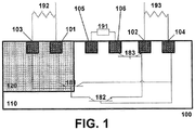
- FIG. 1 shows a first embodiment of a high voltage (HV) electrostatic protection (ESD) protection circuit 100.
- the HV ESD protection circuit 100 comprises regions 101, 104, and 105, which are highly-doped of a first conductivity type. Regions 102, 103, and 106 are highly-doped of a second conductivity type.
- Well region 110 is of the first conductivity type and has a lower doping level than regions 101, 104, and 105.
- Well region 120 is of the second conductivity type and has a lower doping level than regions 102, 103, and 106.
- Highly-doped regions 101 and 103 are formed in well region 120, and highly-doped regions 102, 104, 105, and 106 are formed in well region 110.
- the highly-doped regions 101, 102, 103, 104, 105, and 106 may be separated on the chip surface by field oxide, trench isolation, or equivalent material.
- a semiconductor chip may comprise other circuits in addition to
- Regions 101 (emitter), 110 (collector), and 120 (base) form a first bipolar device 181.
- Regions 102 (emitter), 110 (base), and 120 (collector) form a second bipolar device 182 which is the opposite type of the first bipolar device 181.
- Bipolars 181 and 182 are coupled to form an SCR device.
- Regions 101 and 102 are respectively called the anode and cathode of the SCR device. The spacing between these two regions is referred to as the anode-cathode spacing (LAC).
- Regions 105 and 106 are formed within the LAC. Regions 105 and 106 are coupled by connection 191.
- Connection 191 is a metal contact, via, metal line, resistor, capacitor, diode, metal oxide semiconductor (MOS) device, bipolar, control circuit, or any other electrical element or combination of elements forming a connection between regions 105 and 106.
- Regions 102 (emitter), 106 (collector), and 110 (base) form a bipolar 183.
- Anode 101 may be coupled to region 103 through a resistive element 192.
- cathode 102 may be coupled to region 104 through a resistive element 193.
- the well resistance of region 110 may create a resistive path that couples region 105 to region 104.
- Region 101 is the emitter of bipolar 181.
- bipolar 181 may start to inject collector current into well 110. This current may consist of majority carriers in well 110. The current may be drawn to the cathode 102 through region 104 and resistor 193. The current through resistor 193 may create a voltage difference across the resistor 193 such that the junction between region 110 and region 102 may become forward biased.
- Region 102 is the emitter of both bipolars 182 and 183. Current flowing through bipolar 182 may take the form of collector current in well 120. This current may be drawn from anode 101 through resistor 192 and region 103. The current flowing through resistor 192 may create a voltage difference across the resistor which may forward bias the junction between regions 101 and 120.
- the aforementioned behavior of the current describes a positive feedback loop. Once the junctions are forward biased, for instance by an external trigger current, the positive feedback may keep the SCR device active. If feedback current is high enough to keep the junctions forward biased without the injection of continued, external trigger current, the feedback between bipolars 181 and 182 may be regenerative. The regenerative feedback may keep the SCR device active.
- An SCR may sustain regenerative feedback when the product of the forward gains of the bipolars comprising the SCR, in this case bipolars 181 and 182, is greater than or equal to unity.
- This product is commonly referred to as loop gain. If the loop gain is greater or equal to 1, a small amount of current forced into the base of either bipolar 181 or 182 may be multiplied by the forward gain of the bipolar and injected into the base of the other bipolar. The current may then be multiplied by the forward gain of the other bipolar and injected into the base of the first bipolar. This positive feedback operation may drive the bipolars into saturation, wherein the current may not increase further.
- the holding voltage across the anode and cathode may be 1.2V.
- V A is the Early voltage
- I c is the collector current
- dI c / dV ce is the ratio of the change in the collector current to a change in the collector-emitter voltage.
- Regions 105 and 106 may be viewed as SCR compensation regions by increasing the holding voltage of the SCR in Figure 1 . If regions 105 and 106 were not present between the anode 101 and cathode 102 of the SCR in Figure 1 , the SCR may exhibit a typical holding voltage of 1V to 2V. Adding regions 105 and 106 may introduce a negative feedback mechanism to the SCR device by diverting current away from the SCR device.
- Region 102 serves as the emitter for bipolar 183 as well as bipolar 182.
- Region 110 serves as the base for bipolars 182 and 183. As such, when bipolar 182 conducts current, bipolar 183 may also conduct current.
- Bipolar 183 may be made more efficient than bipolar 182 so that a relatively larger portion of emitter current may be conducted by bipolar 183 than bipolar 182. As such, less collector current of bipolar 182 may contribute to positive feedback which negatively compensates the SCR loop gain.
- the voltage at its collector 106 may be drawn towards the voltage of cathode 102.
- the voltage of region 105 may be drawn towards the voltage of collector 106 depending on the nature of connection 191.
- the voltage of region 105 may be similar to the voltage of region 106.
- the voltage of region 105 may keep the voltage of region 110 low in an area near the collector of bipolar 181.
- the low voltage of region 105 may provide an alternate path for current to flow to cathode 102 rather than through region 104 or bipolar 182.
- the lower local voltage of region 110 may also make it more difficult for the junction of regions 110-102 to become forward-biased. As such, the gain of the SCR feedback mechanism between bipolars 181 and 182 may be reduced, which may be viewed as introducing negative feedback.
- the voltage across the SCR device may be increased which may increase the forward gain of the bipolar devices.
- the SCR may be regenerative. As such, the holding voltage of the SCR depicted in Figure 1 may be higher due to the negative feedback introduced by regions 105 and 106.
- regions 105 and 106 within the LAC of the SCR device may alter the characteristics of the SCR device by affecting the feedback cycle of the SCR device and compensating the SCR device loop gain. Placement of regions 105 and 106 between the anode 101 and cathode 102 of the SCR device significantly impacts the operation of the SCR device.
- Regions 105 and 106 placed in well 110 between the anode 101 and cathode 102 are viewed as effectively being within the base of bipolar 182.
- Bipolar 183 may effectively draw minority carriers from the base of bipolar 182, which may lower the forward gain of bipolar 182. Due to the directionality of the current injection by bipolar 181 into well 110 and by bipolar 182 into well 120, placement of regions 105 and 106 within the LAC as depicted in Figure 1 has a significant effect. Overall the current may flow from anode 101 towards cathode 102. Therefore, regions 105 and 106 are placed directly into this current path which significantly affects the operation of the SCR device. Placement of regions 105 and 106 outside of the LAC would have less of an impact on the performance of the SCR device.
- Regions 105 and 106 placed inside of the LAC may enable bipolar 183 to become stronger relative to bipolar 182. If regions 105 and 106 were placed outside of the LAC, the collector of 183 would no longer be located in the base of bipolar 182. As such, bipolar 183 may have a decreased impact on the positive feedback cycle of the SCR device. Furthermore, the injection of minority carriers from region 102 into well 110 may predominantly occur in the direction of well 120 due to the majority carriers injected by bipolar 181 reaching the junction between well 110 and region 102 from the direction of well 120. If regions 105 and 106 were placed outside of the LAC, bipolar 182 would be favored over bipolar 183.
- Regions 105 and 106 placed within the LAC enable region 105 to be placed within close proximity to the collector junction of bipolar 181 which helps to minimize the well resistance between the collector and region 105.
- placing region 105 outside of the LAC increases the distance between region 105 and the collector junction of bipolar 181.
- the collector junction of bipolar 181 injects current into well 110.
- the increased distance may result in an increased well resistance between the collector junction of bipolar 181 and region 105 which may result in a higher voltage build-up across said resistance.
- the higher voltage build-up would allow the junction between well 110 and region 102 to more easily become forward-biased.
- placement of regions 105 and 106 outside of the LAC reduces their effectiveness by reducing their contribution to the negative feedback of the SCR device.
- the positive feedback of the SCR may be relatively stronger than the negative feedback impact of regions 105 and 106.
- the current may prefer the direct path between anode 101 and cathode 102 than a path through regions 105 and 106, which may lessen their impact.
- the preference for the direct path may result in increasingly stronger positive feedback, further reducing the impact of regions 105 and 106.
- placing regions 105 and 106 within the LAC is preferable to increase the holding voltage.
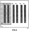
- FIG. 2 shows a top-view of the embodiment of the HV ESD protection circuit 100 shown in Figure 1 .
- regions 101, 110, and 120 form bipolar device 181; regions 102, 110, and 120 form bipolar device 182; and regions 102, 106, and 110 form bipolar 183.
- Regions 101, 102, 103, and 104, 110, and 120 form an SCR device.
- Compensation regions 105 and 106 introduce negative feedback effects which increases the holding voltage of the SCR device.
- the width and length of regions 101 - 106 may be different for each region than depicted in Figures 1 and 2 .
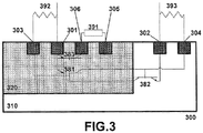
- Figure 3 shows an embodiment of a HV ESD protection circuit 300 wherein compensation regions 305 and 306 are placed within well region 320.
- Region 305 is highly-doped of the second conductivity type and region 306 is highly-doped of the first conductivity type.
- Regions 301, 306, and 320 form bipolar, transistor 383 which competes with bipolar 381 and reduces the effective forward gain of bipolar 381 rather than bipolar 382, which is similarly shown in Figure 1 .
- region 310 may also be applied to region 320.
- the doping levels of regions 310 and 320 may affect the resulting holding voltage.
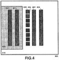
- Figure 4 shows a top view of an embodiment of a HV ESD protection circuit 400 wherein compensation regions 405 and 406 may be implemented in an interleaved fashion rather than in parallel as shown in alternate embodiments.
- the interleaved layout shown may increase the area efficiency by optimizing the layout of compensation regions 405 and 406.
- Regions 405 and 406 are connected by connector elements in a variety of ways to suit a particular desired performance and achieve a desired voltage relationship between the regions.
- Figure 5 shows a top view of an embodiment of a HV ESD protection circuit 500 wherein region 502 may be segmented and compensation region 506 may be extended into spaces between the segments of 502.
- the layout of regions 502 and 506 may increase the effectiveness of bipolar transistor 583 relative to bipolar transistor 582 which may result in a higher holding voltage.
- regions 502 and 506 may be segmented and oriented in the layout shown in Figure 5 , one should recognize alternate layouts are possible which may be preferable for a specific desired behavior of the SCR device.
- Figure 6 shows an embodiment of a HV ESD protection circuit 600 wherein region 606 may be surrounded by a well region 636.
- Region 636 is of the same conductivity as region 606 with a lower doping concentration than region 606.
- region 636 at least touches region 606, and in another embodiment region 636 completely surrounds region 606.
- region 636 may extend compensation region 606 further into the current path between anode 601 and cathode 602.
- Region 636 may also increase the effectiveness of bipolar 683 by increasing the junction area of its collector 606.
- region 636 may be a lowly doped region that may extend deeper into region 610 than region 606.
- region 636 may be the same well type as region 620.
- region 636 may be any well region that extends deeper into region 610 than region 606 and has the same conductivity as region 606. It should be understood that a well region of similar type to well region 636 may be added to or removed from any of the embodiments described herein.
- Figure 8 shows an embodiment of a HV ESD protection circuit 800 similar to the embodiment shown in Figure 6 , wherein HV ESD protection circuit 800 further includes region 835.
- Region 835 is of the same conductivity type as region 805.
- region 835 at least touches region 805, and in another embodiment region 835 completely surrounds region 805.
- region 835 may extend region 805 further into the current path between anode 801 and cathode 802.
- region 835 may be a lowly doped region that may extend deeper into region 810 than region 805.
- Region 805 may have a low voltage and region 835 may extend the low voltage further into region 810 which may cause a larger amount of current to be diverted through bipolar 883 instead of bipolar 882.
- Figure 10 shows an embodiment of a HV ESD protection circuit 1000 incorporating features similar to the embodiments shown in Figure 3 and Figure 6 , wherein the HV ESD protection circuit 1000 may include both compensation regions 1005 and 1006 and compensation regions 1007 and 1008. Regions 1005, 1006, and 1010 form a first compensation bipolar, and regions 1007, 1008, and 1020 may form a second compensation bipolar. Figure 10 depicts a region 1036 which is of the same conductivity as region 1006 and may extend region 1006 similar to how region 636 may extend region 606 in Figure 6 . Inclusion of regions 1005, 1006, 1007, and 1008 may decrease the efficiency of the SCR device which may increase the holding voltage.
- Figure 11 shows an embodiment of a HV ESD protection circuit 1100 similar to the embodiment shown in Figure 10 , wherein compensation regions 1105, 1106, 1107, and 1108 may be located within region 1110. Regions 1105 and 1107 may be of a first conductivity type. Regions 1106 and 1108 may be of a second conductivity type. Regions 1136 and 1138 may be of the second conductivity type and extend regions 1106 and 1108 respectively. While the embodiment shown in Figure 11 depicts 2 coupled pairs of compensation regions, any number of coupled pairs of compensation regions may be placed within the LAC of the SCR device. Adding coupled pairs may increase the holding voltage of the SCR device while increasing the area consumption of the SCR device.
- Figure 13 shows an embodiment of a HV ESD protection circuit 1300 comprising compensation regions 1305 and 1306 which may be coupled by connection element 1391, and compensation regions 1307 and 1308 which may be coupled by connection element 1394.
- the regions may be placed such that region 1305 is between the coupled pair 1307 and 1308, and region 1308 is between the coupled pair 1305 and 1306.
- Figure 15 shows an example, useful for understanding of the present invention, of a HV ESD protection circuit 1500 wherein regions 1507 and 1608 may be of the same conductivity type as region 1506 and may be placed between region 1506 and region 1502. Regions 1507 and 1508 may be coupled by connection element 1594.
- an additional bipolar transistor may be formed by regions 1502, 1508, and 1510. Region 1507 may be viewed as the emitter of bipolar 1583, where in previously described embodiments the emitter of bipolar 1583 was similarly constituted by region 1502.
- the additional bipolar transistor may draw additional highly energetic minority carriers away from region 1510.
- the highly energetic minority carriers collected at region 1508 may be reduced to lower energy minority carriers as they are injected by region 1507 at a higher voltage.
- the lower energy carriers may be more easily collected by region 1506 due to reduced momentum which may increase the effectiveness of bipolar 1583.
- the effectiveness of 1582 may be decreased due to a longer base length resulting from the extra regions 1507 and 1508 within the LAC.
- Figure 15 depicts one pair of coupled regions 1507 and 1508, any number of pairs of similar coupled regions may be placed within the LAC.
- FIG. 16 shows an embodiment of a HV ESD protection circuit 1600 wherein a gate 1694 may be placed between compensation region 1606 and cathode 1602.
- the gate 1694 may block a chip surface isolation layer locally between regions 1602 and 1606 which may increase the effectiveness of bipolar 1683.
- a special layer e.g. shallow trench isolation (STI) block
- STI shallow trench isolation
- FIG. 17 shows an embodiment of a HV ESD protection circuit 1700 wherein a gate 1794 may be placed between compensation regions 1705 and 1706.
- the gate 1794 may block a chip surface isolation layer locally between regions 1705 and 1706 which may improve the connection between regions 1705 and 1706.
- a special layer e.g. shallow trench isolation (STI) block
- STI shallow trench isolation
- Figure 18 shows an example, useful for understanding of the present invention, of a HV ESD protection circuit 1800 wherein compensation region 1806 may be split into regions 1806A and 1806B.
- Compensation region 1805 may be placed between regions 1806A and 1806B.
- Regions 1805, 1806A, and 1806B may be coupled together by connection element 1891.
- connection element 1891 One should recognize various other relative placements of regions 1805, 1806A, and 1806B may be possible within the LAC.
- region 1806 may be split into more than 2 regions.
- Figure 22 shows an embodiment of a HV ESD protection circuit 2200 similar to the embodiments shown in Figures 20 and 21 , wherein an additional region 2212 may be added to separate well region 2220 from buried layer 2221.
- Regions 2210A, 2210B, and 2212 may be of a first conductivity type and regions 2220, 2221, 2222A, and 2222B may be of a second conductivity type.
- region 2201 may be isolated from regions 2223A and 2223B.
- Region 2220 may also be isolated from regions 2221, 2222A, and 2222B by regions 2210A, 2210B, and 2212.
- Regions 2222A and 2222B may be formed by a single well of the second conductivity type.
- Regions 2223A and 2223B may be formed by a single ring region of the second conductivity type.
- Regions 2210A and 2210B may be formed by a single well of the first conductivity type.
- Figure 23 shows an embodiment of a HV ESD protection circuit 2300 wherein control circuits 2394 and/or 2395 may be coupled to compensation regions 2305 and 2306.
- the control circuits may be any of a resistor, capacitor, diode, MOS device, bipolar, or any combination of these elements or any other electrical elements which may be used to alter the behavior of bipolar 2383 formed in part by compensation region 2306.
- the control circuits may alter the resistance of the collector of bipolar 2383 which may affect the operation of bipolar 2383 which, in turn, may impact the feedback of the SCR device.
- the switch may short together regions 2305 and 2306 which may increase the negative feedback introduced by compensation regions 2305 and 2306. Increasing the negative feedback may increase the holding voltage which may avoid latch up during normal chip operation. Though this embodiment has been described for a single compensation region pair 2305 and 2306, one should recognize this technique may be applied to multiple compensation regions introducing multiple negative feedback effects.
- Figure 24 shows an embodiment of a HV ESD protection circuit 2400 comprising external circuits 2492 and 2493 instead of resistors as similarly shown in Figure 6 .
- an external resistance such as resistors 192 and 193 of Figure 1 may not be necessary.
- an external circuit 2492 may be coupled between regions 2401 and 2403, and an external circuit 2493 may be coupled between regions 2402 and 2404.
- the external circuits 2492 and 2493 may control the biasing of well regions 2420 and 2410 respectively.
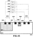
- FIG. 25 shows an embodiment of a HV ESD protection circuit 2500 comprising external triggers 2594-2598.
- An external trigger is a resistor, capacitor, diode, MOS device, bipolar, or any other electrical component or combination of components used to turn on the SCR device. Any one trigger of the triggers 2594-2498 may be present. Also, any combination of the triggers 2594-2598 may be present.
- a trigger is coupled to at least one of regions 2501, 2502, 2503, 2504, 2505, or 2506.
- a trigger may inject current into a region (e.g. a base of a bipolar that makes up the SCR) which may cause junctions of the SCR to become forward biased and turn on the HV ESD protection circuit 2500.
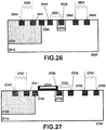
- Figure 26 shows an example, useful for understanding of the present invention, of a HV ESD protection circuit 2600 similar to Figure 6 and comprising region 2609 of the same conductivity type as region 2620.
- the region 2609 may be of the same conductivity type as region 2610. If a voltage in region 2620 relative to region 2610 rises to reach the reverse breakdown voltage of the junction between regions 2620 and 2610, a current may be induced and flow through regions 2603 and 2604 which may be viewed as the trigger taps of the SCR. The induced current may then trigger the SCR device to turn on. Region 2609 may lower the reverse breakdown voltage of the junction between regions 2620 and 2610. One may view region 2609 as a way to adjust the trigger voltage.
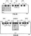
- Figure 28 shows an example, useful for understanding of the present invention, of a HV ESD protection circuit 2800 comprising compensation regions 2805, 2806, and 2807 in the LAC of the SCR device.
- Regions 2805, 2807, and 2810 may be of a first conductivity type and regions 2806 and 2802 may be of a second conductivity type.
- Region 2836 may be a low doped region of the second conductivity type and extend under regions 2806 and 2807.
- a first bipolar may be formed by region 2836 (collector), region 2810 (base), and region 2802 (emitter).
- a second bipolar may be formed by region 2807 (emitter), region 2836 (base), and region 2810 (collector).
- the current may be drawn from region 2806 which may cause a voltage drop in region 2836.
- the voltage drop may cause the junction between regions 2836 and 2807 to become forward biased.
- the forward biased junction may cause the second bipolar to turn on and inject current into region 2810.
- the additional SCR decreases the effectiveness of bipolar 2882 by creating a preferred current path to cathode 2802 which may increase the holding voltage of the SCR device.
- Figure 29 shows an embodiment of a HV ESD protection circuit 2900 comprising a multi-finger structure.
- the left half and right half each constitutes one finger of a two finger structure.
- Region 2903 may be a trigger tap common to both the left half "A" finger and the right half "B" finger.
- Region 2920 may be a lower doped region of the same conductivity type as region 2903 common to both fingers.
- Figure 29 shows an embodiment with two fingers, one should recognize a structure is possible with any number of fingers.
- Figure 30 shows an embodiment of the HV ESD protection circuit 2900 shown in Figure 29 .
- Compensation regions 2905 shown in Figure 29 may be implemented as a single ring region 2905 around region 2920.
- Compensation regions 2906 shown in Figure 29 may be implemented as a single ring region 2906 around region 2905.
- Lower doped regions 2936 extending regions 2906 in Figure 29 may be implemented as region 2936 by surrounding ring region 2906 shown in Figure 30 .
- Figure 31 shows an embodiment of a HV ESD protection circuit 3100 comprising a multi-finger structure.
- the left half and right half each constitutes one finger of a two finger structure.
- Region 3104 may be a trigger tap common to both the left half "A" finger and the right half "B" finger.
- Figure 31 shows an embodiment with two fingers, one should recognize a structure is possible with any number of fingers.
- Figure 31 differs from Figure 29 in that the embodiment shown in Figure 31 may have a central well of a first conductivity type, while the embodiment shown in Figure 29 may have a central well of a second conductivity type.
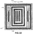
- FIG 32 shows an embodiment of the HV ESD protection circuit 3100 shown in Figure 31 .
- Compensation regions 3106 shown in Figure 31 may be implemented as a single ring region 3106 around regions 3102A, 3102B, and 3104.
- Compensation regions 3105 shown in Figure 31 may be implemented as a single ring region 3105 around region 3106.
- Lower doped regions 3136 extending regions 3106 in Figure 31 may be implemented as region 3136 by surrounding ring region 3106 shown in Figure 32 .
- Regions 3103 shown in Figure 31 may be implemented as a single ring region 3103.
- Regions 3120 shown in Figure 31 may be implemented as a single ring region 3120.
Landscapes
- Semiconductor Integrated Circuits (AREA)
- Metal-Oxide And Bipolar Metal-Oxide Semiconductor Integrated Circuits (AREA)
- Thyristors (AREA)
- Bipolar Integrated Circuits (AREA)
- Emergency Protection Circuit Devices (AREA)
Applications Claiming Priority (2)
| Application Number | Priority Date | Filing Date | Title |
|---|---|---|---|
| US30665810P | 2010-02-22 | 2010-02-22 | |
| PCT/EP2011/052576 WO2011101484A2 (en) | 2010-02-22 | 2011-02-22 | High holding voltage device |
Publications (2)
| Publication Number | Publication Date |
|---|---|
| EP2539934A2 EP2539934A2 (en) | 2013-01-02 |
| EP2539934B1 true EP2539934B1 (en) | 2020-12-16 |
Family
ID=44370630
Family Applications (1)
| Application Number | Title | Priority Date | Filing Date |
|---|---|---|---|
| EP11704784.5A Active EP2539934B1 (en) | 2010-02-22 | 2011-02-22 | High holding voltage device |
Country Status (6)
| Country | Link |
|---|---|
| US (1) | US8653557B2 (enExample) |
| EP (1) | EP2539934B1 (enExample) |
| JP (1) | JP5904644B2 (enExample) |
| CN (1) | CN102884624B (enExample) |
| TW (1) | TW201145488A (enExample) |
| WO (1) | WO2011101484A2 (enExample) |
Families Citing this family (21)
| Publication number | Priority date | Publication date | Assignee | Title |
|---|---|---|---|---|
| EP2812922B1 (en) | 2012-02-07 | 2023-12-20 | Sofics BVBA | Semiconductor device for electrostatic discharge protection having regions of alternating conductivity types |
| CN102569294B (zh) * | 2012-02-28 | 2016-01-13 | 北京燕东微电子有限公司 | 提高静电保护器件维持电压的方法 |
| FR2987938A1 (fr) * | 2012-03-12 | 2013-09-13 | St Microelectronics Sa | Dispositif electronique de protection contre les decharges electrostatiques, a structure concentrique |
| KR101975894B1 (ko) | 2012-12-04 | 2019-08-28 | 삼성전자주식회사 | 정전기 방전 보호 장치 |
| US9502890B2 (en) | 2013-05-22 | 2016-11-22 | Freescale Semiconductor, Inc. | Protection device and related fabrication methods |
| US9129806B2 (en) | 2013-05-22 | 2015-09-08 | Freescale Semiconductor Inc. | Protection device and related fabrication methods |
| JP6052068B2 (ja) * | 2013-06-07 | 2016-12-27 | 株式会社デンソー | 半導体装置の保護回路 |
| US9543420B2 (en) | 2013-07-19 | 2017-01-10 | Nxp Usa, Inc. | Protection device and related fabrication methods |
| US9685431B2 (en) * | 2013-09-27 | 2017-06-20 | Sofics Bvba | Semiconductor device for electrostatic discharge protection |
| TWI548060B (zh) * | 2014-04-23 | 2016-09-01 | 立錡科技股份有限公司 | 為高電壓積體電路提供靜電防護的矽控整流器 |
| US9287255B2 (en) | 2014-07-09 | 2016-03-15 | Freescale Semiconductor Inc. | ESD protection device and related fabrication methods |
| KR102238544B1 (ko) | 2014-12-08 | 2021-04-09 | 삼성전자주식회사 | 정전기 방전 보호 장치 및 이를 포함하는 전자 장치 |
| CN104538436A (zh) * | 2015-01-05 | 2015-04-22 | 武汉新芯集成电路制造有限公司 | 一种高保持电压的可控硅整流器 |
| EP3116027A1 (en) | 2015-07-10 | 2017-01-11 | Nxp B.V. | An electrostatic discharge protection device comprising a silicon controlled rectifier |
| CN105655333A (zh) * | 2016-03-30 | 2016-06-08 | 中国电子科技集团公司第二十四研究所 | 一种高维持电压的双向scr保护结构 |
| EP3451379A1 (en) * | 2017-09-01 | 2019-03-06 | NXP USA, Inc. | Electrostatic discharge protection circuit with a bi-directional silicon controlled rectifier (scr) |
| CN109979931B (zh) * | 2017-12-28 | 2020-11-10 | 无锡华润上华科技有限公司 | 一种双向静电放电保护器件 |
| CN111785717B (zh) * | 2019-04-04 | 2023-05-26 | 中芯国际集成电路制造(上海)有限公司 | Scr静电保护结构及其形成方法 |
| CN113497027B (zh) * | 2020-04-03 | 2024-03-26 | 长鑫存储技术有限公司 | 半导体器件 |
| EP3951884A1 (en) | 2020-08-05 | 2022-02-09 | Nexperia B.V. | A semiconductor device and a method of manufacture of a semiconductor device |
| CN117790500B (zh) * | 2024-02-19 | 2024-05-10 | 成都芯翼科技有限公司 | 一种用于m-lvds端口的静电放电保护结构 |
Citations (1)
| Publication number | Priority date | Publication date | Assignee | Title |
|---|---|---|---|---|
| US20090244797A1 (en) * | 2008-03-27 | 2009-10-01 | Nec Electronics Corporation | Protection circuit |
Family Cites Families (26)
| Publication number | Priority date | Publication date | Assignee | Title |
|---|---|---|---|---|
| JPS58119670A (ja) | 1982-01-11 | 1983-07-16 | Nissan Motor Co Ltd | 半導体装置 |
| US4939616A (en) | 1988-11-01 | 1990-07-03 | Texas Instruments Incorporated | Circuit structure with enhanced electrostatic discharge protection |
| US5274262A (en) | 1989-05-17 | 1993-12-28 | David Sarnoff Research Center, Inc. | SCR protection structure and circuit with reduced trigger voltage |
| US5465189A (en) | 1990-03-05 | 1995-11-07 | Texas Instruments Incorporated | Low voltage triggering semiconductor controlled rectifiers |
| US5268588A (en) | 1992-09-30 | 1993-12-07 | Texas Instruments Incorporated | Semiconductor structure for electrostatic discharge protection |
| US5343053A (en) | 1993-05-21 | 1994-08-30 | David Sarnoff Research Center Inc. | SCR electrostatic discharge protection for integrated circuits |
| US5493133A (en) | 1994-06-30 | 1996-02-20 | Texas Instruments Incorporated | PNP punchthrough-assisted protection device for special applications in CMOS technologies |
| JPH09162298A (ja) | 1995-12-12 | 1997-06-20 | Fujitsu Ltd | 半導体装置 |
| US6172404B1 (en) | 1997-10-31 | 2001-01-09 | Texas Instruments Incorporated | Tuneable holding voltage SCR ESD protection |
| TW411607B (en) | 1998-12-02 | 2000-11-11 | Winbond Electronics Corp | Electrostatic discharge protection circuit |
| US5962876A (en) | 1998-04-06 | 1999-10-05 | Winbond Electronics Corporation | Low voltage triggering electrostatic discharge protection circuit |
| TW393755B (en) | 1998-09-02 | 2000-06-11 | Winbond Electronics Corp | The electrostatic protecting structure of semiconductor |
| US6268639B1 (en) * | 1999-02-11 | 2001-07-31 | Xilinx, Inc. | Electrostatic-discharge protection circuit |
| DE69941977D1 (de) | 1999-06-01 | 2010-03-18 | Imec | ESD-Schutz-Bauteil für mittlere Triggerspannung |
| US6420221B1 (en) * | 2000-02-22 | 2002-07-16 | Taiwan Semiconductor Manufacturing Company | Method of manufacturing a highly latchup-immune CMOS I/O structure |
| US6538266B2 (en) * | 2000-08-11 | 2003-03-25 | Samsung Electronics Co., Ltd. | Protection device with a silicon-controlled rectifier |
| US6433368B1 (en) | 2001-01-22 | 2002-08-13 | National Semiconductor Corporation | LVTSCR with a holding voltage that is greater than a DC bias voltage on a to-be-protected node |
| JP4005920B2 (ja) | 2001-03-16 | 2007-11-14 | サーノフ コーポレーション | ラッチアップ耐性のための高保持電流を有する静電放電保護構造 |
| US6441439B1 (en) | 2001-05-30 | 2002-08-27 | Winbond Electronic Corp. | Low-voltage triggering pseudo bipolar ESD protection device for positive/negative signal input pads |
| US6822294B1 (en) | 2001-06-29 | 2004-11-23 | National Semiconductor Corporation | High holding voltage LVTSCR |
| US20040100745A1 (en) | 2002-11-21 | 2004-05-27 | Industrial Technology Research Institute | Silicon-controlled rectifier with dynamic holding voltage for on-chip electrostatic discharge protection |
| JP3851893B2 (ja) | 2003-08-27 | 2006-11-29 | 株式会社東芝 | 半導体集積回路装置 |
| US7285828B2 (en) * | 2005-01-12 | 2007-10-23 | Intersail Americas Inc. | Electrostatic discharge protection device for digital circuits and for applications with input/output bipolar voltage much higher than the core circuit power supply |
| CN101558498A (zh) | 2005-03-30 | 2009-10-14 | 沙诺夫欧洲公司 | 静电放电保护电路 |
| US7825473B2 (en) * | 2005-07-21 | 2010-11-02 | Industrial Technology Research Institute | Initial-on SCR device for on-chip ESD protection |
| US8247839B2 (en) | 2008-07-09 | 2012-08-21 | Sofics Bvba | ESD protection device with increased holding voltage during normal operation |
-
2011
- 2011-02-17 US US13/029,560 patent/US8653557B2/en active Active
- 2011-02-22 TW TW100105853A patent/TW201145488A/zh unknown
- 2011-02-22 EP EP11704784.5A patent/EP2539934B1/en active Active
- 2011-02-22 WO PCT/EP2011/052576 patent/WO2011101484A2/en not_active Ceased
- 2011-02-22 JP JP2012553345A patent/JP5904644B2/ja active Active
- 2011-02-22 CN CN201180009779.8A patent/CN102884624B/zh active Active
Patent Citations (1)
| Publication number | Priority date | Publication date | Assignee | Title |
|---|---|---|---|---|
| US20090244797A1 (en) * | 2008-03-27 | 2009-10-01 | Nec Electronics Corporation | Protection circuit |
Also Published As
| Publication number | Publication date |
|---|---|
| US8653557B2 (en) | 2014-02-18 |
| WO2011101484A2 (en) | 2011-08-25 |
| WO2011101484A3 (en) | 2011-11-24 |
| JP2013520789A (ja) | 2013-06-06 |
| JP5904644B2 (ja) | 2016-04-13 |
| CN102884624B (zh) | 2015-08-26 |
| EP2539934A2 (en) | 2013-01-02 |
| CN102884624A (zh) | 2013-01-16 |
| US20110204415A1 (en) | 2011-08-25 |
| TW201145488A (en) | 2011-12-16 |
Similar Documents
| Publication | Publication Date | Title |
|---|---|---|
| EP2539934B1 (en) | High holding voltage device | |
| US9041054B2 (en) | High holding voltage electrostatic discharge protection device | |
| CN101506974B (zh) | 利用沟槽隔离形成的无闭锁垂直瞬态电压抑制二极管阵列结构 | |
| US8455315B2 (en) | Symmetric blocking transient voltage suppressor (TVS) using bipolar transistor base snatch | |
| US6858902B1 (en) | Efficient ESD protection with application for low capacitance I/O pads | |
| US20140167099A1 (en) | Integrated circuit including silicon controlled rectifier | |
| US9685431B2 (en) | Semiconductor device for electrostatic discharge protection | |
| US20140363930A1 (en) | Latch-up free vertical tvs diode array structure using trench isolation | |
| CN103975434A (zh) | 高保持电压、混合电压域静电放电钳位 | |
| JP2004221569A (ja) | トリプル・ウェル半導体デバイスの静電放電保護回路 | |
| US7973334B2 (en) | Localized trigger ESD protection device | |
| CN101764151A (zh) | 具有高维持电压的scr esd保护结构 | |
| US8859361B1 (en) | Symmetric blocking transient voltage suppressor (TVS) using bipolar NPN and PNP transistor base snatch | |
| US10665584B1 (en) | Low capacitance and high-holding-voltage transient-voltage-suppressor (TVS) device for electro-static-discharge (ESD) protection | |
| EP2846359B1 (en) | LVTSCR device | |
| CN107546223B (zh) | 一种华夫饼型小岛式二极管触发可控硅静电防护器件 | |
| KR20040090480A (ko) | 내부 회로를 보호하는 보호 회로를 구비한 반도체 장치 | |
| KR102262041B1 (ko) | 정전기 방전 보호소자 | |
| KR102139088B1 (ko) | 높은 홀딩 전류를 갖는 정전기 방전 보호소자 | |
| US20240222959A1 (en) | Electrostatic discharge protection device | |
| KR101258993B1 (ko) | Esd 보호소자 | |
| Tsai et al. | Investigation and solution to the early failure of parasitic NPN triggered by the adjacent PNP ESD clamps | |
| Liu | Design Of Silicon Controlled Rectifers Sic] For Robust Electrostatic Discharge Protection Applications |
Legal Events
| Date | Code | Title | Description |
|---|---|---|---|
| PUAI | Public reference made under article 153(3) epc to a published international application that has entered the european phase |
Free format text: ORIGINAL CODE: 0009012 |
|
| 17P | Request for examination filed |
Effective date: 20120821 |
|
| AK | Designated contracting states |
Kind code of ref document: A2 Designated state(s): AL AT BE BG CH CY CZ DE DK EE ES FI FR GB GR HR HU IE IS IT LI LT LU LV MC MK MT NL NO PL PT RO RS SE SI SK SM TR |
|
| DAX | Request for extension of the european patent (deleted) | ||
| STAA | Information on the status of an ep patent application or granted ep patent |
Free format text: STATUS: EXAMINATION IS IN PROGRESS |
|
| 17Q | First examination report despatched |
Effective date: 20171120 |
|
| GRAP | Despatch of communication of intention to grant a patent |
Free format text: ORIGINAL CODE: EPIDOSNIGR1 |
|
| STAA | Information on the status of an ep patent application or granted ep patent |
Free format text: STATUS: GRANT OF PATENT IS INTENDED |
|
| INTG | Intention to grant announced |
Effective date: 20191017 |
|
| GRAJ | Information related to disapproval of communication of intention to grant by the applicant or resumption of examination proceedings by the epo deleted |
Free format text: ORIGINAL CODE: EPIDOSDIGR1 |
|
| STAA | Information on the status of an ep patent application or granted ep patent |
Free format text: STATUS: EXAMINATION IS IN PROGRESS |
|
| INTC | Intention to grant announced (deleted) | ||
| GRAP | Despatch of communication of intention to grant a patent |
Free format text: ORIGINAL CODE: EPIDOSNIGR1 |
|
| STAA | Information on the status of an ep patent application or granted ep patent |
Free format text: STATUS: GRANT OF PATENT IS INTENDED |
|
| INTG | Intention to grant announced |
Effective date: 20200708 |
|
| GRAS | Grant fee paid |
Free format text: ORIGINAL CODE: EPIDOSNIGR3 |
|
| GRAA | (expected) grant |
Free format text: ORIGINAL CODE: 0009210 |
|
| STAA | Information on the status of an ep patent application or granted ep patent |
Free format text: STATUS: THE PATENT HAS BEEN GRANTED |
|
| AK | Designated contracting states |
Kind code of ref document: B1 Designated state(s): AL AT BE BG CH CY CZ DE DK EE ES FI FR GB GR HR HU IE IS IT LI LT LU LV MC MK MT NL NO PL PT RO RS SE SI SK SM TR |
|
| REG | Reference to a national code |
Ref country code: GB Ref legal event code: FG4D |
|
| REG | Reference to a national code |
Ref country code: IE Ref legal event code: FG4D |
|
| REG | Reference to a national code |
Ref country code: DE Ref legal event code: R096 Ref document number: 602011069646 Country of ref document: DE |
|
| REG | Reference to a national code |
Ref country code: AT Ref legal event code: REF Ref document number: 1346358 Country of ref document: AT Kind code of ref document: T Effective date: 20210115 |
|
| PG25 | Lapsed in a contracting state [announced via postgrant information from national office to epo] |
Ref country code: FI Free format text: LAPSE BECAUSE OF FAILURE TO SUBMIT A TRANSLATION OF THE DESCRIPTION OR TO PAY THE FEE WITHIN THE PRESCRIBED TIME-LIMIT Effective date: 20201216 Ref country code: RS Free format text: LAPSE BECAUSE OF FAILURE TO SUBMIT A TRANSLATION OF THE DESCRIPTION OR TO PAY THE FEE WITHIN THE PRESCRIBED TIME-LIMIT Effective date: 20201216 Ref country code: NO Free format text: LAPSE BECAUSE OF FAILURE TO SUBMIT A TRANSLATION OF THE DESCRIPTION OR TO PAY THE FEE WITHIN THE PRESCRIBED TIME-LIMIT Effective date: 20210316 Ref country code: GR Free format text: LAPSE BECAUSE OF FAILURE TO SUBMIT A TRANSLATION OF THE DESCRIPTION OR TO PAY THE FEE WITHIN THE PRESCRIBED TIME-LIMIT Effective date: 20210317 |
|
| REG | Reference to a national code |
Ref country code: AT Ref legal event code: MK05 Ref document number: 1346358 Country of ref document: AT Kind code of ref document: T Effective date: 20201216 |
|
| REG | Reference to a national code |
Ref country code: NL Ref legal event code: MP Effective date: 20201216 |
|
| PG25 | Lapsed in a contracting state [announced via postgrant information from national office to epo] |
Ref country code: LV Free format text: LAPSE BECAUSE OF FAILURE TO SUBMIT A TRANSLATION OF THE DESCRIPTION OR TO PAY THE FEE WITHIN THE PRESCRIBED TIME-LIMIT Effective date: 20201216 Ref country code: SE Free format text: LAPSE BECAUSE OF FAILURE TO SUBMIT A TRANSLATION OF THE DESCRIPTION OR TO PAY THE FEE WITHIN THE PRESCRIBED TIME-LIMIT Effective date: 20201216 Ref country code: BG Free format text: LAPSE BECAUSE OF FAILURE TO SUBMIT A TRANSLATION OF THE DESCRIPTION OR TO PAY THE FEE WITHIN THE PRESCRIBED TIME-LIMIT Effective date: 20210316 |
|
| PG25 | Lapsed in a contracting state [announced via postgrant information from national office to epo] |
Ref country code: NL Free format text: LAPSE BECAUSE OF FAILURE TO SUBMIT A TRANSLATION OF THE DESCRIPTION OR TO PAY THE FEE WITHIN THE PRESCRIBED TIME-LIMIT Effective date: 20201216 Ref country code: HR Free format text: LAPSE BECAUSE OF FAILURE TO SUBMIT A TRANSLATION OF THE DESCRIPTION OR TO PAY THE FEE WITHIN THE PRESCRIBED TIME-LIMIT Effective date: 20201216 |
|
| REG | Reference to a national code |
Ref country code: LT Ref legal event code: MG9D |
|
| PG25 | Lapsed in a contracting state [announced via postgrant information from national office to epo] |
Ref country code: LT Free format text: LAPSE BECAUSE OF FAILURE TO SUBMIT A TRANSLATION OF THE DESCRIPTION OR TO PAY THE FEE WITHIN THE PRESCRIBED TIME-LIMIT Effective date: 20201216 Ref country code: RO Free format text: LAPSE BECAUSE OF FAILURE TO SUBMIT A TRANSLATION OF THE DESCRIPTION OR TO PAY THE FEE WITHIN THE PRESCRIBED TIME-LIMIT Effective date: 20201216 Ref country code: PT Free format text: LAPSE BECAUSE OF FAILURE TO SUBMIT A TRANSLATION OF THE DESCRIPTION OR TO PAY THE FEE WITHIN THE PRESCRIBED TIME-LIMIT Effective date: 20210416 Ref country code: SK Free format text: LAPSE BECAUSE OF FAILURE TO SUBMIT A TRANSLATION OF THE DESCRIPTION OR TO PAY THE FEE WITHIN THE PRESCRIBED TIME-LIMIT Effective date: 20201216 Ref country code: SM Free format text: LAPSE BECAUSE OF FAILURE TO SUBMIT A TRANSLATION OF THE DESCRIPTION OR TO PAY THE FEE WITHIN THE PRESCRIBED TIME-LIMIT Effective date: 20201216 Ref country code: EE Free format text: LAPSE BECAUSE OF FAILURE TO SUBMIT A TRANSLATION OF THE DESCRIPTION OR TO PAY THE FEE WITHIN THE PRESCRIBED TIME-LIMIT Effective date: 20201216 Ref country code: CZ Free format text: LAPSE BECAUSE OF FAILURE TO SUBMIT A TRANSLATION OF THE DESCRIPTION OR TO PAY THE FEE WITHIN THE PRESCRIBED TIME-LIMIT Effective date: 20201216 |
|
| PG25 | Lapsed in a contracting state [announced via postgrant information from national office to epo] |
Ref country code: PL Free format text: LAPSE BECAUSE OF FAILURE TO SUBMIT A TRANSLATION OF THE DESCRIPTION OR TO PAY THE FEE WITHIN THE PRESCRIBED TIME-LIMIT Effective date: 20201216 Ref country code: AT Free format text: LAPSE BECAUSE OF FAILURE TO SUBMIT A TRANSLATION OF THE DESCRIPTION OR TO PAY THE FEE WITHIN THE PRESCRIBED TIME-LIMIT Effective date: 20201216 |
|
| REG | Reference to a national code |
Ref country code: DE Ref legal event code: R097 Ref document number: 602011069646 Country of ref document: DE |
|
| PG25 | Lapsed in a contracting state [announced via postgrant information from national office to epo] |
Ref country code: MC Free format text: LAPSE BECAUSE OF FAILURE TO SUBMIT A TRANSLATION OF THE DESCRIPTION OR TO PAY THE FEE WITHIN THE PRESCRIBED TIME-LIMIT Effective date: 20201216 Ref country code: IS Free format text: LAPSE BECAUSE OF FAILURE TO SUBMIT A TRANSLATION OF THE DESCRIPTION OR TO PAY THE FEE WITHIN THE PRESCRIBED TIME-LIMIT Effective date: 20210416 |
|
| PLBE | No opposition filed within time limit |
Free format text: ORIGINAL CODE: 0009261 |
|
| STAA | Information on the status of an ep patent application or granted ep patent |
Free format text: STATUS: NO OPPOSITION FILED WITHIN TIME LIMIT |
|
| REG | Reference to a national code |
Ref country code: BE Ref legal event code: MM Effective date: 20210228 |
|
| PG25 | Lapsed in a contracting state [announced via postgrant information from national office to epo] |
Ref country code: LI Free format text: LAPSE BECAUSE OF NON-PAYMENT OF DUE FEES Effective date: 20210228 Ref country code: LU Free format text: LAPSE BECAUSE OF NON-PAYMENT OF DUE FEES Effective date: 20210222 Ref country code: IT Free format text: LAPSE BECAUSE OF FAILURE TO SUBMIT A TRANSLATION OF THE DESCRIPTION OR TO PAY THE FEE WITHIN THE PRESCRIBED TIME-LIMIT Effective date: 20201216 Ref country code: CH Free format text: LAPSE BECAUSE OF NON-PAYMENT OF DUE FEES Effective date: 20210228 Ref country code: AL Free format text: LAPSE BECAUSE OF FAILURE TO SUBMIT A TRANSLATION OF THE DESCRIPTION OR TO PAY THE FEE WITHIN THE PRESCRIBED TIME-LIMIT Effective date: 20201216 |
|
| 26N | No opposition filed |
Effective date: 20210917 |
|
| PG25 | Lapsed in a contracting state [announced via postgrant information from national office to epo] |
Ref country code: DK Free format text: LAPSE BECAUSE OF FAILURE TO SUBMIT A TRANSLATION OF THE DESCRIPTION OR TO PAY THE FEE WITHIN THE PRESCRIBED TIME-LIMIT Effective date: 20201216 Ref country code: ES Free format text: LAPSE BECAUSE OF FAILURE TO SUBMIT A TRANSLATION OF THE DESCRIPTION OR TO PAY THE FEE WITHIN THE PRESCRIBED TIME-LIMIT Effective date: 20201216 |
|
| PG25 | Lapsed in a contracting state [announced via postgrant information from national office to epo] |
Ref country code: IE Free format text: LAPSE BECAUSE OF NON-PAYMENT OF DUE FEES Effective date: 20210222 |
|
| PG25 | Lapsed in a contracting state [announced via postgrant information from national office to epo] |
Ref country code: SI Free format text: LAPSE BECAUSE OF FAILURE TO SUBMIT A TRANSLATION OF THE DESCRIPTION OR TO PAY THE FEE WITHIN THE PRESCRIBED TIME-LIMIT Effective date: 20201216 |
|
| PG25 | Lapsed in a contracting state [announced via postgrant information from national office to epo] |
Ref country code: IS Free format text: LAPSE BECAUSE OF FAILURE TO SUBMIT A TRANSLATION OF THE DESCRIPTION OR TO PAY THE FEE WITHIN THE PRESCRIBED TIME-LIMIT Effective date: 20210416 |
|
| PG25 | Lapsed in a contracting state [announced via postgrant information from national office to epo] |
Ref country code: BE Free format text: LAPSE BECAUSE OF NON-PAYMENT OF DUE FEES Effective date: 20210228 |
|
| PG25 | Lapsed in a contracting state [announced via postgrant information from national office to epo] |
Ref country code: HU Free format text: LAPSE BECAUSE OF FAILURE TO SUBMIT A TRANSLATION OF THE DESCRIPTION OR TO PAY THE FEE WITHIN THE PRESCRIBED TIME-LIMIT; INVALID AB INITIO Effective date: 20110222 Ref country code: CY Free format text: LAPSE BECAUSE OF FAILURE TO SUBMIT A TRANSLATION OF THE DESCRIPTION OR TO PAY THE FEE WITHIN THE PRESCRIBED TIME-LIMIT Effective date: 20201216 |
|
| P01 | Opt-out of the competence of the unified patent court (upc) registered |
Effective date: 20230524 |
|
| PG25 | Lapsed in a contracting state [announced via postgrant information from national office to epo] |
Ref country code: MK Free format text: LAPSE BECAUSE OF FAILURE TO SUBMIT A TRANSLATION OF THE DESCRIPTION OR TO PAY THE FEE WITHIN THE PRESCRIBED TIME-LIMIT Effective date: 20201216 |
|
| PG25 | Lapsed in a contracting state [announced via postgrant information from national office to epo] |
Ref country code: TR Free format text: LAPSE BECAUSE OF FAILURE TO SUBMIT A TRANSLATION OF THE DESCRIPTION OR TO PAY THE FEE WITHIN THE PRESCRIBED TIME-LIMIT Effective date: 20201216 |
|
| PG25 | Lapsed in a contracting state [announced via postgrant information from national office to epo] |
Ref country code: MT Free format text: LAPSE BECAUSE OF FAILURE TO SUBMIT A TRANSLATION OF THE DESCRIPTION OR TO PAY THE FEE WITHIN THE PRESCRIBED TIME-LIMIT Effective date: 20201216 |
|
| REG | Reference to a national code |
Ref country code: DE Ref legal event code: R079 Ref document number: 602011069646 Country of ref document: DE Free format text: PREVIOUS MAIN CLASS: H01L0027020000 Ipc: H10D0089000000 |
|
| PGFP | Annual fee paid to national office [announced via postgrant information from national office to epo] |
Ref country code: DE Payment date: 20250227 Year of fee payment: 15 |
|
| PGFP | Annual fee paid to national office [announced via postgrant information from national office to epo] |
Ref country code: FR Payment date: 20250225 Year of fee payment: 15 |
|
| PGFP | Annual fee paid to national office [announced via postgrant information from national office to epo] |
Ref country code: GB Payment date: 20250227 Year of fee payment: 15 |