EP2526565B1 - Semiconductor packaging method - Google Patents
Semiconductor packaging method Download PDFInfo
- Publication number
- EP2526565B1 EP2526565B1 EP10844172.6A EP10844172A EP2526565B1 EP 2526565 B1 EP2526565 B1 EP 2526565B1 EP 10844172 A EP10844172 A EP 10844172A EP 2526565 B1 EP2526565 B1 EP 2526565B1
- Authority
- EP
- European Patent Office
- Prior art keywords
- lead frame
- die
- leads
- lower lead
- upper lead
- Prior art date
- Legal status (The legal status is an assumption and is not a legal conclusion. Google has not performed a legal analysis and makes no representation as to the accuracy of the status listed.)
- Active
Links
Images
Classifications
-
- H—ELECTRICITY
- H10—SEMICONDUCTOR DEVICES; ELECTRIC SOLID-STATE DEVICES NOT OTHERWISE PROVIDED FOR
- H10W—GENERIC PACKAGES, INTERCONNECTIONS, CONNECTORS OR OTHER CONSTRUCTIONAL DETAILS OF DEVICES COVERED BY CLASS H10
- H10W72/00—Interconnections or connectors in packages
- H10W72/60—Strap connectors, e.g. thick copper clips for grounding of power devices
-
- H—ELECTRICITY
- H10—SEMICONDUCTOR DEVICES; ELECTRIC SOLID-STATE DEVICES NOT OTHERWISE PROVIDED FOR
- H10W—GENERIC PACKAGES, INTERCONNECTIONS, CONNECTORS OR OTHER CONSTRUCTIONAL DETAILS OF DEVICES COVERED BY CLASS H10
- H10W70/00—Package substrates; Interposers; Redistribution layers [RDL]
- H10W70/40—Leadframes
- H10W70/421—Shapes or dispositions
- H10W70/424—Cross-sectional shapes
-
- H—ELECTRICITY
- H10—SEMICONDUCTOR DEVICES; ELECTRIC SOLID-STATE DEVICES NOT OTHERWISE PROVIDED FOR
- H10W—GENERIC PACKAGES, INTERCONNECTIONS, CONNECTORS OR OTHER CONSTRUCTIONAL DETAILS OF DEVICES COVERED BY CLASS H10
- H10W70/00—Package substrates; Interposers; Redistribution layers [RDL]
- H10W70/40—Leadframes
- H10W70/481—Leadframes for devices being provided for in groups H10D8/00 - H10D48/00
-
- H—ELECTRICITY
- H10—SEMICONDUCTOR DEVICES; ELECTRIC SOLID-STATE DEVICES NOT OTHERWISE PROVIDED FOR
- H10W—GENERIC PACKAGES, INTERCONNECTIONS, CONNECTORS OR OTHER CONSTRUCTIONAL DETAILS OF DEVICES COVERED BY CLASS H10
- H10W72/00—Interconnections or connectors in packages
- H10W72/01—Manufacture or treatment
- H10W72/0198—Manufacture or treatment batch processes
-
- H—ELECTRICITY
- H10—SEMICONDUCTOR DEVICES; ELECTRIC SOLID-STATE DEVICES NOT OTHERWISE PROVIDED FOR
- H10W—GENERIC PACKAGES, INTERCONNECTIONS, CONNECTORS OR OTHER CONSTRUCTIONAL DETAILS OF DEVICES COVERED BY CLASS H10
- H10W74/00—Encapsulations, e.g. protective coatings
- H10W74/10—Encapsulations, e.g. protective coatings characterised by their shape or disposition
- H10W74/111—Encapsulations, e.g. protective coatings characterised by their shape or disposition the semiconductor body being completely enclosed
-
- H—ELECTRICITY
- H10—SEMICONDUCTOR DEVICES; ELECTRIC SOLID-STATE DEVICES NOT OTHERWISE PROVIDED FOR
- H10W—GENERIC PACKAGES, INTERCONNECTIONS, CONNECTORS OR OTHER CONSTRUCTIONAL DETAILS OF DEVICES COVERED BY CLASS H10
- H10W72/00—Interconnections or connectors in packages
- H10W72/071—Connecting or disconnecting
- H10W72/076—Connecting or disconnecting of strap connectors
- H10W72/07631—Techniques
- H10W72/07636—Soldering or alloying
-
- H—ELECTRICITY
- H10—SEMICONDUCTOR DEVICES; ELECTRIC SOLID-STATE DEVICES NOT OTHERWISE PROVIDED FOR
- H10W—GENERIC PACKAGES, INTERCONNECTIONS, CONNECTORS OR OTHER CONSTRUCTIONAL DETAILS OF DEVICES COVERED BY CLASS H10
- H10W72/00—Interconnections or connectors in packages
- H10W72/30—Die-attach connectors
-
- H—ELECTRICITY
- H10—SEMICONDUCTOR DEVICES; ELECTRIC SOLID-STATE DEVICES NOT OTHERWISE PROVIDED FOR
- H10W—GENERIC PACKAGES, INTERCONNECTIONS, CONNECTORS OR OTHER CONSTRUCTIONAL DETAILS OF DEVICES COVERED BY CLASS H10
- H10W72/00—Interconnections or connectors in packages
- H10W72/851—Dispositions of multiple connectors or interconnections
- H10W72/874—On different surfaces
- H10W72/877—Bump connectors and die-attach connectors
-
- H—ELECTRICITY
- H10—SEMICONDUCTOR DEVICES; ELECTRIC SOLID-STATE DEVICES NOT OTHERWISE PROVIDED FOR
- H10W—GENERIC PACKAGES, INTERCONNECTIONS, CONNECTORS OR OTHER CONSTRUCTIONAL DETAILS OF DEVICES COVERED BY CLASS H10
- H10W74/00—Encapsulations, e.g. protective coatings
-
- H—ELECTRICITY
- H10—SEMICONDUCTOR DEVICES; ELECTRIC SOLID-STATE DEVICES NOT OTHERWISE PROVIDED FOR
- H10W—GENERIC PACKAGES, INTERCONNECTIONS, CONNECTORS OR OTHER CONSTRUCTIONAL DETAILS OF DEVICES COVERED BY CLASS H10
- H10W90/00—Package configurations
- H10W90/701—Package configurations characterised by the relative positions of pads or connectors relative to package parts
- H10W90/721—Package configurations characterised by the relative positions of pads or connectors relative to package parts of bump connectors
- H10W90/726—Package configurations characterised by the relative positions of pads or connectors relative to package parts of bump connectors between a chip and a stacked lead frame, conducting package substrate or heat sink
-
- H—ELECTRICITY
- H10—SEMICONDUCTOR DEVICES; ELECTRIC SOLID-STATE DEVICES NOT OTHERWISE PROVIDED FOR
- H10W—GENERIC PACKAGES, INTERCONNECTIONS, CONNECTORS OR OTHER CONSTRUCTIONAL DETAILS OF DEVICES COVERED BY CLASS H10
- H10W90/00—Package configurations
- H10W90/701—Package configurations characterised by the relative positions of pads or connectors relative to package parts
- H10W90/761—Package configurations characterised by the relative positions of pads or connectors relative to package parts of strap connectors
- H10W90/766—Package configurations characterised by the relative positions of pads or connectors relative to package parts of strap connectors between a chip and a stacked lead frame, conducting package substrate or heat sink
Definitions
- a number of semiconductor die include terminals on opposite sides of the die.
- vertical power MOSFETs whether of the planar or trench-gated variety, typically have source and gate terminal on the front side of the die and a drain terminal on the back side of the die.
- the die it is advantageous for the die to be packaged such that all the terminals are on the same side of the package.
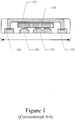
- a conventional package including a die that is interposed flip-chip style, between an upper and lower lead frame is shown in Figure 1 .
- One or more lower leads 110, 115, from a lower lead frame (not shown), are electrically coupled to terminals on the bottom surface of the die 130.
- the upper lead 135, from an upper lead frame (not shown), includes a center portion electrically coupled to a top side of the die 130 and opposite edges, that are bent downward around the die in a 'u' shape or cup shape, electrically coupled to a plurality of respective lower leads 120, 125.
- the terminals of the die 130 are electrically coupled to the lead 110, 115, 135 by means of solder layers.
- the die 130 and portions of upper and lower lead 110-125, 130 are then encapsulated.
- the bent down edges of the upper lead 135 contact multiple lower leads 120, 125, so that all of the external package contacts are coplanar allowing the package to be surface mounted on a printed circuit board.
- US2008036078 discloses a wirebond-less packaged semiconductor device that includes a plurality of I/O contacts and at least one semiconductor die, the semiconductor die having a bottom major surface and a top major surface, the top major surface having at least two electrically isolated electrodes, and a conductive clip system disposed over the top major surface, the clip system comprising at least two electrically isolated sections coupling the electrodes to respective I/O contacts.
- US 2002/121684 discloses a semiconductor device X1 that comprises: a first conductor 110 including a first terminal surface 113a; a second conductor 120 placed by the first conductor 110 and including a second terminal surface 123a facing a same direction as does the first terminal surface 113a; a third conductor 130 connected with the first conductor 110; a semiconductor chip 140 including a first surface 141 and a second surface 142 away from the first surface, and bonded to the first conductor 110 and to the second conductor 120 via the second surface 142; and a resin package 150.
- the first surface 141 of the semiconductor chip 140 is provided with a first electrode electrically connected with the first conductor 110 via the third conductor 130.
- the second surface 142 is provided with a second electrode electrically connected directly with the second conductor 120.;
- the resin package 150 seals the first conductor 110, the second conductor 120, the third conductor 130 and the semiconductor chip 140 while exposing the first terminal surface 113a and the second terminal surface 123a.
- US 7,238,551 discloses a semiconductor package that includes a die that is interposed, flip-chip style, between an upper lead frame and a lower lead frame.
- the lower lead frame has contacts that are aligned with terminals on the bottom surface of the die.
- the upper lead frame contacts a terminal on the top side of the die, and the edges of the upper lead frame are bent downward around the edges of the die, giving the upper lead frame a cup shape.
- the edge of the upper lead frame contact another portion of the lower lead frame, so that all of the contacts of the package are coplanar and can be surface-mounted on a printed circuit board.
- the terminals of the die are electrically connected to the lead frames by means of solder layers.
- the thicknesses of the respective solder layers that connect the die to the lead frames are predetermined to optimize the performance of the package through numerous thermal cycles. This is done by fabricating the lower lead frame with a plurality of mesas and using a double solder reflow process.
- US 2008/233679 discloses a semiconductor package and method for making a semiconductor package.
- the semiconductor package has a top surface and a mounting surface and includes a die, a conducting connecting material, a plating material and an insulating material.
- the die has a processed surface facing towards the mounting surface of the semiconductor package. Exposed metal connections are at the processed surface of the die.
- the conducting connecting material is disposed on the exposed metal connections.
- the plating material is in contact with the conducting connecting material.
- the insulating material is formed around the conducting connecting material, and the plating material extends to the exterior of the insulating material.
- US 2004/063240 discloses a semiconductor die package including a semiconductor die comprising a first surface, a second surface, and a vertical power MOSFET having a gate region and a source region at the first surface a drain region at the second surface.
- a drain clip having a major surface is electrically coupled to the drain region.
- a gate lead is electrically coupled to the gate region.
- a source lead is electrically coupled to the source region.
- a non-conductive molding material encapsulates the semiconductor die. The major surface of the drain clip is exposed through the non-conductive molding material.
- Embodiments of the present technology are directed toward a flip-chip style semiconductor package including a die, one or more lower leads and one or more upper 'L' shaped leads, and a method of manufacturing.
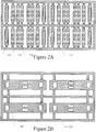
- the lower lead frame includes one or more leads 210-220, for each of a plurality of die, coupled by one or more tie bars 225.
- the upper lead frame also includes one or more leads 230 coupled by one or more tie bars 235.
- the lower lead frame may include a source lead, a gate lead and a lower portion of a drain lead for each die, and the upper lead frame may include an upper portion of a drain lead for each die.
- Each set of a source lead, gate lead and lower portion of a drain lead in the lower lead frame is typically referred to as a panel.
- each upper portion of the drain lead in the upper lead frame is typically referred to as a panel.
- the lead frame normally includes a large array of panels.
- the upper and lower lead frames may be made formed from a sheet of copper alloy 194 that is approximately 0.006 to 0.012 inches thick.
- the pattern of the leads and tie bars may be formed by etching, punching, stamping and/or the like.
- the lower lead frame may be partially etched to form a plurality of raised mesas on the source and/or gate leads.
- the etching process may also be used to form cavities in the lower portion of the drain leads.
- the mesas and cavities may be formed by etching the copper alloy of the lower lead frame with a chemical solution to a thickness of approximately one half of its original thickness.
- the mesas and cavities may be formed by progressive stamping. Different patterns of raised mesas may be formed on the lower lead frame.
- the upper lead frame may be partially etched to form one or more grooves (not shown) on the lower surface. The grooves may improve the compliance of the upper lead with the semiconductor die during thermal cycles.
- the grooves may be formed as one or more parallel and/or perpendicular grooves.
- forming too many grooves in the upper leads may increase the risk of dies cracking during the molding process, because the flat central portion of the upper lead protects the die from differential forces that might crack the die during molding.
- the die may be a vertical trench MOSFET with a drain terminal on the top surface of the die and a source and gate terminal on the lower surface of the die.
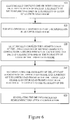
- One or more leads 210-22 of the lower lead frame are electrically coupled to respective terminals on the die 130 by a conductor such as a solder layer, at 610.
- the leads are coupled to the terminal of the die by a solder reflow process after solder paste is applied to the source and gate leads.
- the solder layer extends from the top surfaces of mesas on the source and gate leads to respective contacts on the die.
- the solder layer may also be applied to the lower portion of the drain lead at the same time as it is applied to the source and gate leads and may flow into the groove in the lower portion of the drain lead when the solder layer is reflowed to coupled the source and gate leads to the respective terminals of the die.
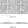
- FIG. 4A and 4B a top and side view of coupling the upper lead frame to the lower lead frame and the plurality of die, in accordance with one embodiment of the present technology, is shown.
- one or more edges of the leads of the upper lead frame are bent to form 'L' shaped leads for contact one or more leads of the lower lead frame, at 620.
- the opposite edges of each pair of leads, coupled together by the second set of tie bars, in the upper lead frame are bent to form 'L' shaped upper portions of drain leads.
- each lead of the upper lead frame is electrically coupled to respective terminals on a set of die by a conductor such as a solder layer.
- the bent edges of the leads are coupled to respective leads on the lower lead frame.
- the edges of the upper portion of the drain leads are electrically coupled to respective lower portions of the drain leads of the lower lead frame.
- the upper portion of the drain leads are coupled to corresponding terminals of the die and the lower portion of the drain leads by a solder reflow process after solder paste is applied to the terminals of the die and the lower portion of the drain leads of the lower lead frame.
- the relative thickness of the solder layer coupling the upper lead frame to the die and the thickness of the solder layer coupling the lower lead frame to the die are set such that the resulting package is able to undergo numerous thermal cycles without fracture or cracks in either solder layer.
- the upper solder layer is thinner than the lower solder layer because the upper solder layer has a wider area of contact between the leads of the upper lead frame and the die.
- the relative proportions between the thickness of the upper solder layer and the lower solder layer may be achieved by a double-reflow process. In accordance with this process, drops of a solder paste are first applied to the lower lead frame, typically on the tops of the mesas.
- solder paste drops are applied to the top side of the die.
- solder paste may also be placed on the portions of the lower lead frames that will be coupled to the bent portions of the leads of the upper lead frame.
- the upper lead frame is placed into position over the die, resting on the solder paste drops on the backside of the die and then a second reflow process is performed. As the solder past reflows, the die are lifted from the lower lead frame to a position intermediate between the upper lead frame and the lower lead frame. This lifting of the die occurs as a result of the surface tension of the solder.
- the desired position of the die may be further achieved.
- the ratio of the thickness between the upper solder layer and the lower solder layer is in the range of 1:1.5 to 1:4.
- the upper solder layer may be 1.1 mils thick and the lower solder layer may be 2.8 mils thick.
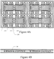
- the assembly including the lower lead frame, plurality of die, and upper lead frame, after solder is applied, is then be encapsulated, at 640.
- the assembly is placed in a mold that is then filled with a molding compound, such as Nitto 8000CH4.
- a molding compound such as Nitto 8000CH4.
- the upper surface of the panels from the upper lead frame may be left exposed by the encapsulant to maximize heat transfer from the package.
- the encapsulated panels of the upper lead frame, die and lower lead frame are then separated by severing the tie bars of the lower and upper lead frames, at 650.
- the upper lead of each packaged die has a substantially 'L' shape.
- the die are separate by cutting through the encapsulant and tie bars of the upper and lower lead frame between the die to form the packaged semiconductor device.
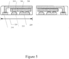
- each package semiconductor includes a die 130 electrically coupled to one or more of a plurality of lower leads 215, 220, an 'L' shaped upper lead 230 electrically coupled between the die 130 and another one of the plurality of lower leads 210, an encapsulant 510.
- the upper lead is coupled to a lower lead on one side and is not coupled to another lower lead on the other side of the die. Therefore, the semiconductor device, in accordance with embodiments of the present technology, have a smaller package size 520 as compared to similar semiconductor packages according to the conventional art.
- different sawing arrangements may be utilized to produce different paired packages with different lead layouts (e.g., pin outs).
- the resulting package advantageously provides excellent electrical and thermal conductivity between the terminals on the top and bottom sides of the die and the upper and lower lead frames respectively.
- the contacts from the terminals on the top and bottom side of the die are advantageously located in a single plane of the package for surface mounting on a printed circuit board or other flat surface.
- the package can advantageously be made thin and compact and is able to withstand numerous thermal cycles without solder or die cracking.
- Embodiments of the present technology advantageously support the upper lead without the need for an additional lower lead in each package. All elements, parts and steps described herein are preferably included. It is to be understood that any of these elements, parts and steps may be replaced by other elements, parts and steps or deleted all together as will be obvious to those skilled in the art.
- this writing discloses semiconductors packaged by electrically coupling a plurality of die to an upper and lower lead frame.
- the opposite edges of each corresponding set of leads in the upper lead frame are bent.
- the leads in the upper lead frame are electrically coupled between respective contacts on respective die and respective lower portion of the leads in the lower lead frame.
- the bent opposite edges of each corresponding set of leads of the upper lead frame support the upper lead frame before encapsulation, for achieving a desired position of the plurality of die between the leads of the upper and lower lead frames in the packaged semiconductor.
- the upper leads After the encapsulated die are separated, have an L-shape and electrically couple die contacts on upper side of the die to leads on the lower side of the die so that the package contacts are on the same side of the semiconductor package.
Landscapes
- Lead Frames For Integrated Circuits (AREA)
- Structures Or Materials For Encapsulating Or Coating Semiconductor Devices Or Solid State Devices (AREA)
- Wire Bonding (AREA)
- Encapsulation Of And Coatings For Semiconductor Or Solid State Devices (AREA)
Applications Claiming Priority (3)
| Application Number | Priority Date | Filing Date | Title |
|---|---|---|---|
| US29647110P | 2010-01-19 | 2010-01-19 | |
| US12/730,230 US8586419B2 (en) | 2010-01-19 | 2010-03-24 | Semiconductor packages including die and L-shaped lead and method of manufacture |
| PCT/US2010/059326 WO2011090574A2 (en) | 2010-01-19 | 2010-12-07 | Semiconductor package and method |
Publications (3)
| Publication Number | Publication Date |
|---|---|
| EP2526565A2 EP2526565A2 (en) | 2012-11-28 |
| EP2526565A4 EP2526565A4 (en) | 2014-03-05 |
| EP2526565B1 true EP2526565B1 (en) | 2019-02-20 |
Family
ID=44276982
Family Applications (1)
| Application Number | Title | Priority Date | Filing Date |
|---|---|---|---|
| EP10844172.6A Active EP2526565B1 (en) | 2010-01-19 | 2010-12-07 | Semiconductor packaging method |
Country Status (6)
| Country | Link |
|---|---|
| US (1) | US8586419B2 (enExample) |
| EP (1) | EP2526565B1 (enExample) |
| JP (2) | JP5607758B2 (enExample) |
| KR (1) | KR101534463B1 (enExample) |
| CN (1) | CN102714201B (enExample) |
| WO (1) | WO2011090574A2 (enExample) |
Families Citing this family (23)
| Publication number | Priority date | Publication date | Assignee | Title |
|---|---|---|---|---|
| TWI453831B (zh) | 2010-09-09 | 2014-09-21 | 台灣捷康綜合有限公司 | 半導體封裝結構及其製造方法 |
| JP5333402B2 (ja) * | 2010-10-06 | 2013-11-06 | 三菱電機株式会社 | 半導体装置の製造方法 |
| CN102394232A (zh) * | 2011-11-29 | 2012-03-28 | 杭州矽力杰半导体技术有限公司 | 一种引线框架及应用其的芯片倒装封装装置 |
| US9966330B2 (en) | 2013-03-14 | 2018-05-08 | Vishay-Siliconix | Stack die package |
| US9589929B2 (en) | 2013-03-14 | 2017-03-07 | Vishay-Siliconix | Method for fabricating stack die package |
| JP6245485B2 (ja) * | 2013-03-14 | 2017-12-13 | ヴィシェイ−シリコニックス | スタックダイパッケージを製造する方法 |
| CN103395735B (zh) * | 2013-08-05 | 2015-12-02 | 天津大学 | 微机电系统器件的封装结构 |
| CN103681582B (zh) * | 2013-12-05 | 2016-03-30 | 江苏长电科技股份有限公司 | 一次先蚀后镀金属框减法埋芯片正装凸点结构及工艺方法 |
| CN103646937B (zh) * | 2013-12-05 | 2016-02-24 | 江苏长电科技股份有限公司 | 二次先蚀后镀金属框减法埋芯片倒装凸点结构及工艺方法 |
| CN103646930B (zh) * | 2013-12-05 | 2016-02-24 | 江苏长电科技股份有限公司 | 二次先蚀后镀金属框减法埋芯片倒装平脚结构及工艺方法 |
| CN103646938B (zh) * | 2013-12-05 | 2016-02-24 | 江苏长电科技股份有限公司 | 一次先镀后蚀金属框减法埋芯片倒装凸点结构及工艺方法 |
| CN103646931B (zh) * | 2013-12-05 | 2016-06-29 | 江苏长电科技股份有限公司 | 一次先镀后蚀金属框减法埋芯片倒装平脚结构及工艺方法 |
| JP2015176871A (ja) * | 2014-03-12 | 2015-10-05 | 株式会社東芝 | 半導体装置及びその製造方法 |
| US9425304B2 (en) | 2014-08-21 | 2016-08-23 | Vishay-Siliconix | Transistor structure with improved unclamped inductive switching immunity |
| CN104952737B (zh) * | 2015-06-30 | 2017-12-26 | 通富微电子股份有限公司 | 一种具有铝带或l脚或凸起的封装框架结构及生产方法 |
| KR101734712B1 (ko) * | 2015-12-09 | 2017-05-11 | 현대자동차주식회사 | 파워모듈 |
| US9870985B1 (en) * | 2016-07-11 | 2018-01-16 | Amkor Technology, Inc. | Semiconductor package with clip alignment notch |
| JP6892796B2 (ja) * | 2017-07-07 | 2021-06-23 | 新光電気工業株式会社 | 電子部品装置及びその製造方法 |
| DE102019103281B4 (de) * | 2019-02-11 | 2023-03-16 | Infineon Technologies Ag | Verfahren zum bilden eines die-gehäuses |
| CN111725173A (zh) * | 2020-06-05 | 2020-09-29 | 杰群电子科技(东莞)有限公司 | 一种堆叠封装结构及堆叠封装结构的制造方法 |
| US20240112990A1 (en) * | 2020-12-23 | 2024-04-04 | Rohm Co., Ltd. | Method for manufacturing semiconductor apparatus and semiconductor apparatus |
| US12142548B2 (en) * | 2021-12-30 | 2024-11-12 | Alpha And Omega Semiconductor International Lp | Semiconductor package having mold locking feature |
| CN219123228U (zh) * | 2023-01-06 | 2023-06-02 | 上海凯虹科技电子有限公司 | 引线框架及封装结构 |
Family Cites Families (19)
| Publication number | Priority date | Publication date | Assignee | Title |
|---|---|---|---|---|
| JPH11177007A (ja) * | 1997-12-15 | 1999-07-02 | Hitachi Ltd | トランジスタパッケージ |
| JP4450800B2 (ja) * | 1999-02-17 | 2010-04-14 | 株式会社ルネサステクノロジ | 半導体装置の製造方法 |
| JP3314768B2 (ja) * | 1999-10-26 | 2002-08-12 | サンケン電気株式会社 | 半導体装置及びその製造方法 |
| JP2002222890A (ja) * | 2001-01-25 | 2002-08-09 | Rohm Co Ltd | 半導体装置およびその製造方法 |
| US6734536B2 (en) * | 2001-01-12 | 2004-05-11 | Rohm Co., Ltd. | Surface-mounting semiconductor device and method of making the same |
| US6777800B2 (en) * | 2002-09-30 | 2004-08-17 | Fairchild Semiconductor Corporation | Semiconductor die package including drain clip |
| US7132734B2 (en) * | 2003-01-06 | 2006-11-07 | Micron Technology, Inc. | Microelectronic component assemblies and microelectronic component lead frame structures |
| JP4294405B2 (ja) * | 2003-07-31 | 2009-07-15 | 株式会社ルネサステクノロジ | 半導体装置 |
| US7394150B2 (en) * | 2004-11-23 | 2008-07-01 | Siliconix Incorporated | Semiconductor package including die interposed between cup-shaped lead frame and lead frame having mesas and valleys |
| DE112005002899B4 (de) * | 2004-11-23 | 2016-11-17 | Siliconix Inc. | Halbleiterbauelement mit einem Chip, der zwischen einer becherförmigen Leiterplatte und einer Leiterplatte mit Mesas und Tälern angeordnet ist, und Verfahren zur dessen Herstellung |
| US7238551B2 (en) * | 2004-11-23 | 2007-07-03 | Siliconix Incorporated | Method of fabricating semiconductor package including die interposed between cup-shaped lead frame having mesas and valleys |
| US20060108635A1 (en) | 2004-11-23 | 2006-05-25 | Alpha Omega Semiconductor Limited | Trenched MOSFETS with part of the device formed on a (110) crystal plane |
| US7394151B2 (en) * | 2005-02-15 | 2008-07-01 | Alpha & Omega Semiconductor Limited | Semiconductor package with plated connection |
| US20070132073A1 (en) * | 2005-12-09 | 2007-06-14 | Tiong Toong T | Device and method for assembling a top and bottom exposed packaged semiconductor |
| CN101326636A (zh) * | 2005-12-09 | 2008-12-17 | 飞兆半导体公司 | 用于组装顶部与底部暴露的封装半导体的装置和方法 |
| US7271470B1 (en) * | 2006-05-31 | 2007-09-18 | Infineon Technologies Ag | Electronic component having at least two semiconductor power devices |
| US20080036078A1 (en) * | 2006-08-14 | 2008-02-14 | Ciclon Semiconductor Device Corp. | Wirebond-less semiconductor package |
| JP4365856B2 (ja) * | 2006-12-21 | 2009-11-18 | 株式会社オティックス | カムシャフトの支持構造及び支持部材 |
| US8035221B2 (en) * | 2007-11-08 | 2011-10-11 | Intersil Americas, Inc. | Clip mount for integrated circuit leadframes |
-
2010
- 2010-03-24 US US12/730,230 patent/US8586419B2/en active Active
- 2010-12-07 KR KR1020127017726A patent/KR101534463B1/ko active Active
- 2010-12-07 EP EP10844172.6A patent/EP2526565B1/en active Active
- 2010-12-07 CN CN201080061500.6A patent/CN102714201B/zh active Active
- 2010-12-07 WO PCT/US2010/059326 patent/WO2011090574A2/en not_active Ceased
- 2010-12-07 JP JP2012548940A patent/JP5607758B2/ja active Active
-
2014
- 2014-08-28 JP JP2014173498A patent/JP2015057823A/ja active Pending
Non-Patent Citations (1)
| Title |
|---|
| None * |
Also Published As
| Publication number | Publication date |
|---|---|
| EP2526565A2 (en) | 2012-11-28 |
| WO2011090574A3 (en) | 2011-09-22 |
| CN102714201B (zh) | 2015-12-09 |
| KR101534463B1 (ko) | 2015-07-07 |
| US20110175217A1 (en) | 2011-07-21 |
| EP2526565A4 (en) | 2014-03-05 |
| JP5607758B2 (ja) | 2014-10-15 |
| CN102714201A (zh) | 2012-10-03 |
| JP2015057823A (ja) | 2015-03-26 |
| US8586419B2 (en) | 2013-11-19 |
| JP2013517624A (ja) | 2013-05-16 |
| WO2011090574A2 (en) | 2011-07-28 |
| KR20120125462A (ko) | 2012-11-15 |
Similar Documents
| Publication | Publication Date | Title |
|---|---|---|
| EP2526565B1 (en) | Semiconductor packaging method | |
| CN101656250B (zh) | 具有立体匹配互连板的紧密封装半导体芯片 | |
| CN101443906B (zh) | 具有夹在杯状引线框和具台面和谷的引线框之间的管芯的半导体封装 | |
| JP4878030B2 (ja) | エッチング処理されたリードフレームを用いる再分散型ハンダパッド | |
| US8344499B2 (en) | Chip-exposed semiconductor device | |
| US8436429B2 (en) | Stacked power semiconductor device using dual lead frame and manufacturing method | |
| US11948870B2 (en) | Low stress asymmetric dual side module | |
| US8963302B2 (en) | Stacked packaged integrated circuit devices, and methods of making same | |
| US7095096B1 (en) | Microarray lead frame | |
| US9401318B2 (en) | Quad flat no-lead package and manufacturing method thereof | |
| JP6534677B2 (ja) | スタックされたチップ及びインターポーザを備えた部分的に薄化されたリードフレームを有するコンバータ | |
| US9281265B2 (en) | Packaging structure of a semiconductor device | |
| CN103824784B (zh) | 用连接片实现连接的半导体封装的方法 | |
| JP2012238737A (ja) | 半導体モジュール及びその製造方法 | |
| TWI427750B (zh) | 包括晶粒及l形引線之半導體封裝及其製造方法 | |
| CN114783883B (zh) | 一种功率封装结构及其制造方法 | |
| CN120319731A (zh) | 半导体封装结构 | |
| TWI244744B (en) | Flat package for circuit components having soldered metallic contact terminal blocks with lateral surface and process of fabricating the same | |
| CN205488099U (zh) | 半导体装置 | |
| HK1135232B (en) | Method of forming a semiconductor package and structure therefor | |
| CN101009348A (zh) | 表面贴装型半导体二极管装置 |
Legal Events
| Date | Code | Title | Description |
|---|---|---|---|
| PUAI | Public reference made under article 153(3) epc to a published international application that has entered the european phase |
Free format text: ORIGINAL CODE: 0009012 |
|
| 17P | Request for examination filed |
Effective date: 20120814 |
|
| AK | Designated contracting states |
Kind code of ref document: A2 Designated state(s): AL AT BE BG CH CY CZ DE DK EE ES FI FR GB GR HR HU IE IS IT LI LT LU LV MC MK MT NL NO PL PT RO RS SE SI SK SM TR |
|
| DAX | Request for extension of the european patent (deleted) | ||
| A4 | Supplementary search report drawn up and despatched |
Effective date: 20140203 |
|
| RIC1 | Information provided on ipc code assigned before grant |
Ipc: H01L 23/31 20060101ALI20140128BHEP Ipc: H01L 23/495 20060101AFI20140128BHEP |
|
| 17Q | First examination report despatched |
Effective date: 20160115 |
|
| STAA | Information on the status of an ep patent application or granted ep patent |
Free format text: STATUS: EXAMINATION IS IN PROGRESS |
|
| GRAJ | Information related to disapproval of communication of intention to grant by the applicant or resumption of examination proceedings by the epo deleted |
Free format text: ORIGINAL CODE: EPIDOSDIGR1 |
|
| STAA | Information on the status of an ep patent application or granted ep patent |
Free format text: STATUS: GRANT OF PATENT IS INTENDED |
|
| GRAP | Despatch of communication of intention to grant a patent |
Free format text: ORIGINAL CODE: EPIDOSNIGR1 |
|
| INTG | Intention to grant announced |
Effective date: 20180717 |
|
| GRAS | Grant fee paid |
Free format text: ORIGINAL CODE: EPIDOSNIGR3 |
|
| GRAA | (expected) grant |
Free format text: ORIGINAL CODE: 0009210 |
|
| STAA | Information on the status of an ep patent application or granted ep patent |
Free format text: STATUS: THE PATENT HAS BEEN GRANTED |
|
| AK | Designated contracting states |
Kind code of ref document: B1 Designated state(s): AL AT BE BG CH CY CZ DE DK EE ES FI FR GB GR HR HU IE IS IT LI LT LU LV MC MK MT NL NO PL PT RO RS SE SI SK SM TR |
|
| REG | Reference to a national code |
Ref country code: GB Ref legal event code: FG4D |
|
| REG | Reference to a national code |
Ref country code: CH Ref legal event code: EP |
|
| REG | Reference to a national code |
Ref country code: AT Ref legal event code: REF Ref document number: 1099299 Country of ref document: AT Kind code of ref document: T Effective date: 20190315 |
|
| REG | Reference to a national code |
Ref country code: IE Ref legal event code: FG4D |
|
| REG | Reference to a national code |
Ref country code: DE Ref legal event code: R096 Ref document number: 602010057132 Country of ref document: DE |
|
| REG | Reference to a national code |
Ref country code: LT Ref legal event code: MG4D Ref country code: NL Ref legal event code: MP Effective date: 20190220 |
|
| PG25 | Lapsed in a contracting state [announced via postgrant information from national office to epo] |
Ref country code: NO Free format text: LAPSE BECAUSE OF FAILURE TO SUBMIT A TRANSLATION OF THE DESCRIPTION OR TO PAY THE FEE WITHIN THE PRESCRIBED TIME-LIMIT Effective date: 20190520 Ref country code: FI Free format text: LAPSE BECAUSE OF FAILURE TO SUBMIT A TRANSLATION OF THE DESCRIPTION OR TO PAY THE FEE WITHIN THE PRESCRIBED TIME-LIMIT Effective date: 20190220 Ref country code: LT Free format text: LAPSE BECAUSE OF FAILURE TO SUBMIT A TRANSLATION OF THE DESCRIPTION OR TO PAY THE FEE WITHIN THE PRESCRIBED TIME-LIMIT Effective date: 20190220 Ref country code: PT Free format text: LAPSE BECAUSE OF FAILURE TO SUBMIT A TRANSLATION OF THE DESCRIPTION OR TO PAY THE FEE WITHIN THE PRESCRIBED TIME-LIMIT Effective date: 20190620 Ref country code: SE Free format text: LAPSE BECAUSE OF FAILURE TO SUBMIT A TRANSLATION OF THE DESCRIPTION OR TO PAY THE FEE WITHIN THE PRESCRIBED TIME-LIMIT Effective date: 20190220 |
|
| PG25 | Lapsed in a contracting state [announced via postgrant information from national office to epo] |
Ref country code: LV Free format text: LAPSE BECAUSE OF FAILURE TO SUBMIT A TRANSLATION OF THE DESCRIPTION OR TO PAY THE FEE WITHIN THE PRESCRIBED TIME-LIMIT Effective date: 20190220 Ref country code: NL Free format text: LAPSE BECAUSE OF FAILURE TO SUBMIT A TRANSLATION OF THE DESCRIPTION OR TO PAY THE FEE WITHIN THE PRESCRIBED TIME-LIMIT Effective date: 20190220 Ref country code: RS Free format text: LAPSE BECAUSE OF FAILURE TO SUBMIT A TRANSLATION OF THE DESCRIPTION OR TO PAY THE FEE WITHIN THE PRESCRIBED TIME-LIMIT Effective date: 20190220 Ref country code: IS Free format text: LAPSE BECAUSE OF FAILURE TO SUBMIT A TRANSLATION OF THE DESCRIPTION OR TO PAY THE FEE WITHIN THE PRESCRIBED TIME-LIMIT Effective date: 20190620 Ref country code: BG Free format text: LAPSE BECAUSE OF FAILURE TO SUBMIT A TRANSLATION OF THE DESCRIPTION OR TO PAY THE FEE WITHIN THE PRESCRIBED TIME-LIMIT Effective date: 20190520 Ref country code: GR Free format text: LAPSE BECAUSE OF FAILURE TO SUBMIT A TRANSLATION OF THE DESCRIPTION OR TO PAY THE FEE WITHIN THE PRESCRIBED TIME-LIMIT Effective date: 20190521 Ref country code: HR Free format text: LAPSE BECAUSE OF FAILURE TO SUBMIT A TRANSLATION OF THE DESCRIPTION OR TO PAY THE FEE WITHIN THE PRESCRIBED TIME-LIMIT Effective date: 20190220 |
|
| REG | Reference to a national code |
Ref country code: AT Ref legal event code: MK05 Ref document number: 1099299 Country of ref document: AT Kind code of ref document: T Effective date: 20190220 |
|
| PG25 | Lapsed in a contracting state [announced via postgrant information from national office to epo] |
Ref country code: DK Free format text: LAPSE BECAUSE OF FAILURE TO SUBMIT A TRANSLATION OF THE DESCRIPTION OR TO PAY THE FEE WITHIN THE PRESCRIBED TIME-LIMIT Effective date: 20190220 Ref country code: EE Free format text: LAPSE BECAUSE OF FAILURE TO SUBMIT A TRANSLATION OF THE DESCRIPTION OR TO PAY THE FEE WITHIN THE PRESCRIBED TIME-LIMIT Effective date: 20190220 Ref country code: AL Free format text: LAPSE BECAUSE OF FAILURE TO SUBMIT A TRANSLATION OF THE DESCRIPTION OR TO PAY THE FEE WITHIN THE PRESCRIBED TIME-LIMIT Effective date: 20190220 Ref country code: SK Free format text: LAPSE BECAUSE OF FAILURE TO SUBMIT A TRANSLATION OF THE DESCRIPTION OR TO PAY THE FEE WITHIN THE PRESCRIBED TIME-LIMIT Effective date: 20190220 Ref country code: IT Free format text: LAPSE BECAUSE OF FAILURE TO SUBMIT A TRANSLATION OF THE DESCRIPTION OR TO PAY THE FEE WITHIN THE PRESCRIBED TIME-LIMIT Effective date: 20190220 Ref country code: RO Free format text: LAPSE BECAUSE OF FAILURE TO SUBMIT A TRANSLATION OF THE DESCRIPTION OR TO PAY THE FEE WITHIN THE PRESCRIBED TIME-LIMIT Effective date: 20190220 Ref country code: ES Free format text: LAPSE BECAUSE OF FAILURE TO SUBMIT A TRANSLATION OF THE DESCRIPTION OR TO PAY THE FEE WITHIN THE PRESCRIBED TIME-LIMIT Effective date: 20190220 Ref country code: CZ Free format text: LAPSE BECAUSE OF FAILURE TO SUBMIT A TRANSLATION OF THE DESCRIPTION OR TO PAY THE FEE WITHIN THE PRESCRIBED TIME-LIMIT Effective date: 20190220 |
|
| REG | Reference to a national code |
Ref country code: DE Ref legal event code: R097 Ref document number: 602010057132 Country of ref document: DE |
|
| PG25 | Lapsed in a contracting state [announced via postgrant information from national office to epo] |
Ref country code: SM Free format text: LAPSE BECAUSE OF FAILURE TO SUBMIT A TRANSLATION OF THE DESCRIPTION OR TO PAY THE FEE WITHIN THE PRESCRIBED TIME-LIMIT Effective date: 20190220 Ref country code: PL Free format text: LAPSE BECAUSE OF FAILURE TO SUBMIT A TRANSLATION OF THE DESCRIPTION OR TO PAY THE FEE WITHIN THE PRESCRIBED TIME-LIMIT Effective date: 20190220 |
|
| PLBE | No opposition filed within time limit |
Free format text: ORIGINAL CODE: 0009261 |
|
| STAA | Information on the status of an ep patent application or granted ep patent |
Free format text: STATUS: NO OPPOSITION FILED WITHIN TIME LIMIT |
|
| PG25 | Lapsed in a contracting state [announced via postgrant information from national office to epo] |
Ref country code: AT Free format text: LAPSE BECAUSE OF FAILURE TO SUBMIT A TRANSLATION OF THE DESCRIPTION OR TO PAY THE FEE WITHIN THE PRESCRIBED TIME-LIMIT Effective date: 20190220 |
|
| 26N | No opposition filed |
Effective date: 20191121 |
|
| PG25 | Lapsed in a contracting state [announced via postgrant information from national office to epo] |
Ref country code: SI Free format text: LAPSE BECAUSE OF FAILURE TO SUBMIT A TRANSLATION OF THE DESCRIPTION OR TO PAY THE FEE WITHIN THE PRESCRIBED TIME-LIMIT Effective date: 20190220 |
|
| PG25 | Lapsed in a contracting state [announced via postgrant information from national office to epo] |
Ref country code: TR Free format text: LAPSE BECAUSE OF FAILURE TO SUBMIT A TRANSLATION OF THE DESCRIPTION OR TO PAY THE FEE WITHIN THE PRESCRIBED TIME-LIMIT Effective date: 20190220 |
|
| REG | Reference to a national code |
Ref country code: DE Ref legal event code: R119 Ref document number: 602010057132 Country of ref document: DE |
|
| REG | Reference to a national code |
Ref country code: CH Ref legal event code: PL |
|
| REG | Reference to a national code |
Ref country code: BE Ref legal event code: MM Effective date: 20191231 |
|
| PG25 | Lapsed in a contracting state [announced via postgrant information from national office to epo] |
Ref country code: MC Free format text: LAPSE BECAUSE OF FAILURE TO SUBMIT A TRANSLATION OF THE DESCRIPTION OR TO PAY THE FEE WITHIN THE PRESCRIBED TIME-LIMIT Effective date: 20190220 |
|
| GBPC | Gb: european patent ceased through non-payment of renewal fee |
Effective date: 20191207 |
|
| PG25 | Lapsed in a contracting state [announced via postgrant information from national office to epo] |
Ref country code: GB Free format text: LAPSE BECAUSE OF NON-PAYMENT OF DUE FEES Effective date: 20191207 Ref country code: DE Free format text: LAPSE BECAUSE OF NON-PAYMENT OF DUE FEES Effective date: 20200701 Ref country code: LU Free format text: LAPSE BECAUSE OF NON-PAYMENT OF DUE FEES Effective date: 20191207 Ref country code: IE Free format text: LAPSE BECAUSE OF NON-PAYMENT OF DUE FEES Effective date: 20191207 |
|
| PG25 | Lapsed in a contracting state [announced via postgrant information from national office to epo] |
Ref country code: LI Free format text: LAPSE BECAUSE OF NON-PAYMENT OF DUE FEES Effective date: 20191231 Ref country code: CH Free format text: LAPSE BECAUSE OF NON-PAYMENT OF DUE FEES Effective date: 20191231 Ref country code: BE Free format text: LAPSE BECAUSE OF NON-PAYMENT OF DUE FEES Effective date: 20191231 |
|
| PG25 | Lapsed in a contracting state [announced via postgrant information from national office to epo] |
Ref country code: CY Free format text: LAPSE BECAUSE OF FAILURE TO SUBMIT A TRANSLATION OF THE DESCRIPTION OR TO PAY THE FEE WITHIN THE PRESCRIBED TIME-LIMIT Effective date: 20190220 |
|
| PG25 | Lapsed in a contracting state [announced via postgrant information from national office to epo] |
Ref country code: MT Free format text: LAPSE BECAUSE OF FAILURE TO SUBMIT A TRANSLATION OF THE DESCRIPTION OR TO PAY THE FEE WITHIN THE PRESCRIBED TIME-LIMIT Effective date: 20190220 Ref country code: HU Free format text: LAPSE BECAUSE OF FAILURE TO SUBMIT A TRANSLATION OF THE DESCRIPTION OR TO PAY THE FEE WITHIN THE PRESCRIBED TIME-LIMIT; INVALID AB INITIO Effective date: 20101207 |
|
| PG25 | Lapsed in a contracting state [announced via postgrant information from national office to epo] |
Ref country code: MK Free format text: LAPSE BECAUSE OF FAILURE TO SUBMIT A TRANSLATION OF THE DESCRIPTION OR TO PAY THE FEE WITHIN THE PRESCRIBED TIME-LIMIT Effective date: 20190220 |
|
| PGFP | Annual fee paid to national office [announced via postgrant information from national office to epo] |
Ref country code: FR Payment date: 20251226 Year of fee payment: 16 |