EP2519979B1 - Optoelektronischer halbleiterchip mit zwei auf algan basierenden zwischenschichten - Google Patents
Optoelektronischer halbleiterchip mit zwei auf algan basierenden zwischenschichten Download PDFInfo
- Publication number
- EP2519979B1 EP2519979B1 EP10798083.1A EP10798083A EP2519979B1 EP 2519979 B1 EP2519979 B1 EP 2519979B1 EP 10798083 A EP10798083 A EP 10798083A EP 2519979 B1 EP2519979 B1 EP 2519979B1
- Authority
- EP
- European Patent Office
- Prior art keywords
- layer sequence
- intermediate layers
- semiconductor chip
- layers
- layer
- Prior art date
- Legal status (The legal status is an assumption and is not a legal conclusion. Google has not performed a legal analysis and makes no representation as to the accuracy of the status listed.)
- Active
Links
Images


Classifications
-
- H—ELECTRICITY
- H10—SEMICONDUCTOR DEVICES; ELECTRIC SOLID-STATE DEVICES NOT OTHERWISE PROVIDED FOR
- H10H—INORGANIC LIGHT-EMITTING SEMICONDUCTOR DEVICES HAVING POTENTIAL BARRIERS
- H10H20/00—Individual inorganic light-emitting semiconductor devices having potential barriers, e.g. light-emitting diodes [LED]
- H10H20/80—Constructional details
- H10H20/81—Bodies
- H10H20/822—Materials of the light-emitting regions
- H10H20/824—Materials of the light-emitting regions comprising only Group III-V materials, e.g. GaP
- H10H20/825—Materials of the light-emitting regions comprising only Group III-V materials, e.g. GaP containing nitrogen, e.g. GaN
-
- H—ELECTRICITY
- H10—SEMICONDUCTOR DEVICES; ELECTRIC SOLID-STATE DEVICES NOT OTHERWISE PROVIDED FOR
- H10H—INORGANIC LIGHT-EMITTING SEMICONDUCTOR DEVICES HAVING POTENTIAL BARRIERS
- H10H20/00—Individual inorganic light-emitting semiconductor devices having potential barriers, e.g. light-emitting diodes [LED]
- H10H20/01—Manufacture or treatment
- H10H20/011—Manufacture or treatment of bodies, e.g. forming semiconductor layers
- H10H20/013—Manufacture or treatment of bodies, e.g. forming semiconductor layers having light-emitting regions comprising only Group III-V materials
- H10H20/0133—Manufacture or treatment of bodies, e.g. forming semiconductor layers having light-emitting regions comprising only Group III-V materials with a substrate not being Group III-V materials
- H10H20/01335—Manufacture or treatment of bodies, e.g. forming semiconductor layers having light-emitting regions comprising only Group III-V materials with a substrate not being Group III-V materials the light-emitting regions comprising nitride materials
-
- H—ELECTRICITY
- H10—SEMICONDUCTOR DEVICES; ELECTRIC SOLID-STATE DEVICES NOT OTHERWISE PROVIDED FOR
- H10H—INORGANIC LIGHT-EMITTING SEMICONDUCTOR DEVICES HAVING POTENTIAL BARRIERS
- H10H20/00—Individual inorganic light-emitting semiconductor devices having potential barriers, e.g. light-emitting diodes [LED]
- H10H20/01—Manufacture or treatment
- H10H20/011—Manufacture or treatment of bodies, e.g. forming semiconductor layers
- H10H20/018—Bonding of wafers
-
- H—ELECTRICITY
- H10—SEMICONDUCTOR DEVICES; ELECTRIC SOLID-STATE DEVICES NOT OTHERWISE PROVIDED FOR
- H10H—INORGANIC LIGHT-EMITTING SEMICONDUCTOR DEVICES HAVING POTENTIAL BARRIERS
- H10H20/00—Individual inorganic light-emitting semiconductor devices having potential barriers, e.g. light-emitting diodes [LED]
- H10H20/80—Constructional details
- H10H20/81—Bodies
- H10H20/815—Bodies having stress relaxation structures, e.g. buffer layers
-
- H—ELECTRICITY
- H10—SEMICONDUCTOR DEVICES; ELECTRIC SOLID-STATE DEVICES NOT OTHERWISE PROVIDED FOR
- H10H—INORGANIC LIGHT-EMITTING SEMICONDUCTOR DEVICES HAVING POTENTIAL BARRIERS
- H10H20/00—Individual inorganic light-emitting semiconductor devices having potential barriers, e.g. light-emitting diodes [LED]
- H10H20/80—Constructional details
- H10H20/81—Bodies
- H10H20/817—Bodies characterised by the crystal structures or orientations, e.g. polycrystalline, amorphous or porous
-
- H—ELECTRICITY
- H10—SEMICONDUCTOR DEVICES; ELECTRIC SOLID-STATE DEVICES NOT OTHERWISE PROVIDED FOR
- H10H—INORGANIC LIGHT-EMITTING SEMICONDUCTOR DEVICES HAVING POTENTIAL BARRIERS
- H10H20/00—Individual inorganic light-emitting semiconductor devices having potential barriers, e.g. light-emitting diodes [LED]
- H10H20/80—Constructional details
- H10H20/81—Bodies
- H10H20/819—Bodies characterised by their shape, e.g. curved or truncated substrates
- H10H20/82—Roughened surfaces, e.g. at the interface between epitaxial layers
-
- H—ELECTRICITY
- H10—SEMICONDUCTOR DEVICES; ELECTRIC SOLID-STATE DEVICES NOT OTHERWISE PROVIDED FOR
- H10H—INORGANIC LIGHT-EMITTING SEMICONDUCTOR DEVICES HAVING POTENTIAL BARRIERS
- H10H20/00—Individual inorganic light-emitting semiconductor devices having potential barriers, e.g. light-emitting diodes [LED]
- H10H20/80—Constructional details
- H10H20/81—Bodies
- H10H20/8215—Bodies characterised by crystalline imperfections, e.g. dislocations; characterised by the distribution of dopants, e.g. delta-doping
-
- H—ELECTRICITY
- H01—ELECTRIC ELEMENTS
- H01L—SEMICONDUCTOR DEVICES NOT COVERED BY CLASS H10
- H01L2924/00—Indexing scheme for arrangements or methods for connecting or disconnecting semiconductor or solid-state bodies as covered by H01L24/00
- H01L2924/0001—Technical content checked by a classifier
- H01L2924/0002—Not covered by any one of groups H01L24/00, H01L24/00 and H01L2224/00
Definitions
- An optoelectronic semiconductor chip with intermediate layers based on AlGaN is specified.
- the publication EP 1 505 698 A2 relates to a semiconductor device with a superlattice.
- a group III nitride semiconductor multilayer structure can be found in the document EP 2 019 437 A1 ,
- One problem to be solved is to provide an optoelectronic semiconductor chip which is highly impervious to liquid chemicals.
- the present invention is defined in claim 1.
- the optoelectronic semiconductor chip comprises an epitaxially grown semiconductor layer sequence based on AlGaN and / or InAlGaN. Based means that the semiconductor layer sequence predominantly has or consists of at least one of the materials mentioned. This does not rule out that the semiconductor layer sequence can have comparatively small amounts of further substances, in particular dopants.
- the semiconductor layer sequence comprises a p-doped layer sequence, an n-doped layer sequence and an active zone which is located between the p-doped layer sequence and the n-doped layer sequence.
- layer sequence does not rule out that the layer sequence has only a single layer which is homogeneous in terms of its physical properties.
- a layer is to be understood as an area which extends in a direction perpendicular to a growth direction of the semiconductor layer sequence over the entire semiconductor layer sequence or over a predominant part of the semiconductor layer sequence, for example over more than 80%.
- a layer can therefore be a plane-shaped region of the semiconductor layer sequence oriented perpendicular to a growth direction with a specific physical property, such as a specific material composition.
- a sharp transition means in particular that a transition region between the layers or regions with regard to their physical properties, such as a material composition, takes place within the scope of the manufacturing tolerances and / or is at most five monolayers, in particular at most two monolayers of a crystal structure.
- the active zone is set up to generate electromagnetic radiation in the ultraviolet, in the visible and / or in the near-infrared spectral range during operation of the semiconductor chip.
- a main wavelength of the radiation generated by the active zone during operation of the semiconductor chip lies at wavelengths between and including 380 nm and 550 nm.
- the main wavelength is the wavelength at which the radiation generated in the active zone has a maximum intensity per nm spectral width.
- Radiation emitted by the semiconductor chip and generated in the active zone is furthermore preferably incoherent radiation.
- the semiconductor chip is then designed as a light-emitting diode and not as a laser diode or as a superluminescent diode.
- the semiconductor layer sequence contains two intermediate layers which are based on Al x Ga 1 - x N.
- the intermediate layers are layers based on GaN, in which a certain proportion of Ga lattice sites are occupied by Al atoms.
- the intermediate layers are on the same side of the active zone as the n-doped layer sequence.
- one of the intermediate layers is undoped.
- Undoped means in particular that a Dopant concentration is less than 5 x 10 16 per cm 3 .
- the intermediate layer can then directly adjoin the n-doped layer sequence.
- a material of the intermediate layer is then in direct contact with an n-doped material of the n-doped layer sequence.
- the intermediate layer is preferably located within the semiconductor layer sequence, so that the intermediate layer does not form a boundary surface of the semiconductor layer sequence in a direction parallel to the growth direction.
- the intermediate layers are located within the n-doped layer sequence.
- the fact that the intermediate layers are located within the n-doped layer sequence means that the intermediate layers on both sides border on further, n-doped regions of the n-doped layer sequence.
- the intermediate layers then do not form a boundary surface of the n-doped layer sequence in a direction parallel to the growth direction.
- a specific chemical permeability of the intermediate layers is smaller than for regions or layers of the semiconductor layer sequence adjacent to the intermediate layers.
- the intermediate layers have a specific chemical permeability which corresponds to a minimum specific chemical permeability of the entire semiconductor layer sequence or the entire n-doped layer sequence.
- Specific chemical permeability means permeability, based on a certain geometrical thickness of the layer and over a certain period of time, to liquids with a particularly low viscosity. Small viscosity can mean that the liquid has a viscosity of at most 2.5 mPas. What is meant here are in particular liquids or chemicals that do not decompose the intermediate layers.
- the intermediate layers are impermeable to nitric acid compared to the rest of the semiconductor layer sequence.
- the intermediate layers are also preferably impermeable to vapors.
- the intermediate layers preferably inhibit the diffusion of metals such as silver or the intermediate layers are not penetrated by metals by diffusion or, in comparison to the other layers of the semiconductor layer sequence, penetrate to a lesser extent.
- the optoelectronic semiconductor chip comprises an epitaxially grown semiconductor layer sequence based on AlGaN and / or InAlGaN.
- the semiconductor layer sequence includes a p-doped layer sequence, an n-doped layer sequence and an active zone which is provided for generating electromagnetic radiation and which is located between the p-doped and the n-doped layer sequence.
- the semiconductor layer sequence comprises Al x Ga 1 - x N-based, non-doped or n-doped intermediate layers.
- the intermediate layers are located within the semiconductor layer sequence and have a specific chemical permeability to nitric acid which is less than a specific chemical permeability of regions or layers of the semiconductor layer sequence adjacent to the intermediate layers.
- the permeability of layers of the semiconductor layer sequence to liquid chemicals or to vapors is caused, for example, by dislocations such as so-called threading dislocations, which can form channels or holes in the semiconductor material.
- the cracks are dislocation lines, for example.
- the AlGaN of the intermediate layers can accumulate in and / or on the holes and / or cracks, as a result of which the cracks and / or holes and / or cores of the dislocation lines can be reduced.
- layers of the n-doped layer sequence or the semiconductor layer sequence adjacent to the intermediate layers have cracks and / or holes which extend transversely to a main direction of expansion of the intermediate layers.
- a lateral direction that is, a direction perpendicular to a growth direction of the semiconductor layer sequence
- the cracks and / or the holes have lateral dimensions on the nanometer scale or the micrometer scale.
- the extent of the holes and / or cracks in a lateral direction is, for example, at most 25 nm or at most 50 nm or at most 0.10 ⁇ m or at most 0.25 ⁇ m or at most 0.40 ⁇ m.
- the intermediate layers close off at least some of the cracks and / or the holes.
- the intermediate layers completely cover at least some of the holes and / or the cracks.
- the intermediate layers have elevations which extend away from the active zone and / or towards the active zone Extend cracks and / or into the holes.
- the elevations which are preferably formed with the same material as the intermediate layers, are in places in direct, direct, physical contact with a material of the layer into which the cracks and / or the holes extend.
- the intermediate layers reduce a diameter and / or a span of the holes and / or cracks. That is, at least a part of the cracks and / or holes, for example more than 80% or more than 95% or more than 99% of the holes and / or cracks, are smaller after the intermediate layer than in front of the intermediate layers, as seen along the growth direction. This includes the fact that the holes and / or cracks are completely covered and / or blocked and / or interrupted by the intermediate layers.
- the holes and / or cracks extend at least in part further after the intermediate layers.
- the intermediate layers it is possible for the intermediate layers to seal the holes and / or cracks against the penetration of liquid chemicals, but not to remove the holes and / or cracks as impurities in the crystal lattice, so that the cracks and / or holes are at least partially on both sides of the intermediate layers available.
- the number of holes, as seen in the growth direction, immediately after the intermediate layers is at least 50% or at least 75% or at least 90% and / or at most 90% or at most 95% of the number of holes immediately before the Interlayers.
- the cracks or dislocation lines it is possible that these are completely eliminated by the intermediate layers or their number is reduced by at least 50% or by at least 75% or by at least 90%.
- Semiconductor layer sequences for optoelectronic semiconductor chips, in particular for light-emitting diodes, are epitaxially grown, for example, on sapphire substrates.
- holes in particular can arise in the semiconductor material to be grown.
- cracks can also arise in a laser lifting process, in which the fully grown semiconductor layer sequence is removed from the substrate.
- the holes and / or cracks on a boundary surface of the semiconductor layer sequence formerly facing the substrate can be exposed, for example in the laser lifting process itself or when a roughening is generated, for example by means of wet etching, so that at least some of the holes and / or cracks thus form this boundary surface Semiconductor layer sequence is sufficient.
- a liquid chemical can penetrate the semiconductor layer sequence in a subsequent process step and in particular attack a mirror, for example a silver mirror, which was previously applied to a side of the semiconductor layer sequence facing away from the growth substrate or to a plated-through hole. Damage to the mirror in this way reduces the light output efficiency.
- the cracks and / or holes which also represent defects in the semiconductor layer sequence, can furthermore reduce efficiency in generating the radiation in the active zone. Likewise, through the cracks and / or holes small current problems occur in the current-voltage characteristic of the semiconductor chip.
- AlGaN layers can have a smoothing effect on a surface morphology when growing compared to pure GaN layers , AlGaN layers thus react significantly less sensitive to facet growth than GaN layers, as a result of which holes, cracks and / or channels that are present in a GaN crystal can be closed or reduced by such an AlGaN layer.
- one of the intermediate layers is with a dopant concentration between 2 x 10 18 per cm 3 and 5 x 10 19 per cm 3 , preferably with a dopant concentration between 4 x 10 18 per cm 3 and 3 x 10 19 per cm 3 , in particular between 6 x 10 18 per cm 3 and 2 x 10 19 per cm 3 .
- Doping takes place, for example, with Si atoms.
- the fraction x of the Ga lattice sites which is occupied by Al atoms has a value between 0.03 and 0.5 inclusive, preferably between 0.07 and 0.13 inclusive, for example around 0.1.
- the intermediate layers have a thickness of between 15 nm and 250 nm or between 15 nm and 200 nm, in particular between 25 nm and 100 nm.
- one of the intermediate layers is an uninterrupted, continuous layer.
- no openings or breakthroughs are then specifically made in this intermediate layer in a direction perpendicular to the growth direction.
- This intermediate layer therefore extends in a direction perpendicular to the growth direction over the entire semiconductor layer sequence without there being any deliberately generated interruptions.
- the fact that this intermediate layer is an uninterrupted, continuous layer does not rule out that defects in the crystal lattice of the semiconductor layer sequence, such as cracks and / or holes, form small, unintentional openings in this intermediate layer. In other words, it is possible that not all of the cracks and / or holes are closed by this intermediate layer. However, preferably no such unintentional openings occur.
- At least one electrical via penetrates the active zone and one of the intermediate layers which are formed in the semiconductor layer sequence.
- all the electrical contacts for energizing the semiconductor chip it is possible for all the electrical contacts for energizing the semiconductor chip to be located on only one side of the active zone.
- the semiconductor chip can then be shaped as a so-called flip chip.
- a distance from an outer boundary surface of the semiconductor layer sequence to a mirror, for example at the via is comparatively small and is, for example, approximately 2 ⁇ m.
- the intermediate layers based on AlGaN border on both sides on GaN layers which have no Al content. At least one of these GaN layers is preferably doped higher than the intermediate layer in question and is formed, for example, as a current spreading layer. The other of these GaN layers can have a dopant concentration that is at least a factor of 2 lower than the relevant intermediate layer.
- the optoelectronic semiconductor chip comprises exactly two of the intermediate layers. There are then preferably no further layers in the semiconductor layer sequence which have a material composition corresponding to the intermediate layers.
- the intermediate layers are not part of a so-called superlattice.
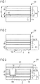
- FIG. 1 A modification of an optoelectronic semiconductor chip 100 is shown.
- the semiconductor chip 100 is in particular a light-emitting diode which emits incoherent radiation during operation.
- a semiconductor layer sequence 1 has grown epitaxially on a growth substrate 11.
- the semiconductor layer sequence 1 is based on AlGaN and / or InAlGaN.
- a total thickness G of the semiconductor layer sequence 1 is, for example, between 1.0 ⁇ m and 10 ⁇ m, in particular between 1.5 ⁇ m and 7.0 ⁇ m, in particular approximately 5 ⁇ m to 6 ⁇ m.
- An undoped GaN layer 15 is located directly on the growth substrate 11.
- the undoped layer 15 has, for example, a thickness between and including 300 nm 400 nm.
- An n-doped sublayer 17 is produced on a side of the undoped layer 15 facing away from the growth substrate 11 and is part of an n-doped layer sequence 4 of the semiconductor layer sequence 1. It is possible that only one of the layers 15, 17 is present.
- An active zone 3 is located on a side of the growth substrate 11 facing away from the n-doped layer sequence 4, followed by a p-doped layer sequence 2.
- the active zone 2 is located between the n-doped layer sequence 4 and the p-doped layer sequence 2 in particular at least one quantum well structure of any dimensionality, preferably several quantum well structures. For example, ultraviolet radiation, blue or green light is generated in the active zone during operation.
- the n-doped layer sequence 4 contains an intermediate layer 5.
- the intermediate layer 5 is located within the n-doped layer sequence 4 between the sub-layer 17 and an n-doped current expansion layer 7, which is also part of the n-doped layer sequence 4.
- the intermediate layer 5 has no direct contact with the growth substrate 11 or with the active zone 3.
- a minimum thickness of the undoped layer 15 and / or the sub-layer 17 is therefore to be set at least such that the growth substrate 11 is essentially completely covered by at least one of these layers 15, 17 and a side of these layers 15, 17 facing away from the growth substrate 11 is essentially is just shaped.
- a thickness T of the intermediate layer 5 is between 25 nm and 150 nm inclusive.
- the intermediate layer 5 is based on AlGaN, a proportion of 3% inclusive up to 20%, in particular about 10%, of the gallium lattice sites, compared to pure GaN, is occupied by aluminum atoms.
- a dopant concentration of the intermediate layer in this modification is preferably between 4 ⁇ 10 18 per cm 3 and 5 ⁇ 10 19 per cm 3 , especially between 6 ⁇ 10 18 per cm 3 and 2 ⁇ 10 19 per cm 3 .
- An example of a dopant is silicon.
- the intermediate layer 5 is a closed, continuous layer. In other words, no openings or openings are deliberately created in the intermediate layer 5.
- a buffer layer 6 of the semiconductor layer sequence 1 is formed by the partial layer 17, the intermediate layer 5 and the current spreading layer 7 and thus comprises the n-doped layer sequence 4.
- a thickness of the buffer layer 6 is, for example, between 300 nm and 6 ⁇ m, preferably between 500 inclusive nm and 1.8 ⁇ m.
- a thickness of the buffer layer 6 exceeds a thickness of the p-doped layer sequence 2, which according to the exemplary embodiment Figure 1 is formed only by a single layer, preferably by at least a factor of 10 or by at least a factor of 20.
- a p-contact layer 12p is applied to a side 20 of the p-doped layer sequence 2 facing away from the active zone 3.
- the p-contact layer 12p is in particular formed by one or more metallic layers and can represent and / or comprise a mirror 16 for a radiation generated in the active zone 3.
- a carrier 9 is attached, which mechanically seals the semiconductor chip 100 wearing.
- a thickness of the carrier 9 is preferably between 40 ⁇ m and 600 ⁇ m inclusive. The carrier 9 makes it possible to handle the semiconductor chip 100, for example by means of a so-called pick-and-place process.
- a roughening 8 is produced on a side 40 of the partial layer 17 of the n-doped layer sequence 4 facing away from the active zone 3, for example by means of etching.
- the roughening 8 does not extend to the intermediate layer 5 Figure 1 be completely removed.
- a coupling-out efficiency of the radiation from the semiconductor chip 100 can be increased via the roughening 8.
- An average roughness of the roughening 8 is preferably between 0.4 ⁇ m and 4.0 ⁇ m, in particular between 0.5 ⁇ m and 1.5 ⁇ m.
- an n-contact 12n is applied to the side 40 in which the roughening 8 is formed.
- the n-contact 12n is formed in particular by one or more metallic layers and / or by a transparent conductive oxide.
- the n contact 12n is a so-called bond pad.
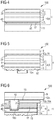
- a current flow takes place accordingly Figure 2 also through the intermediate layer 5, so that it is necessary to make the intermediate layer 5 electrically conductive, that is to say in particular n-doped.
- the semiconductor chip 100 according to Figure 2 can according to the semiconductor chip 100 Figure 1 be generated as follows: after the growth of the semiconductor layer sequence 100 on the growth substrate 11, the p-contact 12p and then on the p-contact 12p of the carrier 9 are attached. Subsequently, the growth substrate 11, in particular by means of a laser lift-off process, is removed from the semiconductor layer sequence 1 and the Carrier 9 removed. In this case, a thin area of the n-doped layer sequence 4, which is located near the growth substrate 11, is decomposed, in particular a part of the undoped layer 15 Partial layer 17 of the n-doped layer sequence 4 is formed on the side 40.
- n-contact 12n and the p-contact 12p are the n-contact 12n and the p-contact 12p on the same side of the active zone 3. This is made possible in particular that, starting from the n-contact 12n, a via 10 through the p-doped layer sequence 2 and through active zone 3 is formed towards the n-layer sequence 4.
- the via 10 can be formed by one or more metals. Via the via 10, a direct electrical connection between the n-contact 12n, which is formed between the carrier 9 and the p-contact 12p, and the current expansion layer 7 of the n-doped layer sequence 4 is established.
- the n-contact 12n and the via 10 are separated from the active zone 3, the p-doped layer sequence 2 and the p-contact 12p by an electrically insulating layer 13, which is formed, for example, with a transparent material such as silicon dioxide or silicon nitride ,
- the p-contact 12p serves as a mirror 16a for the radiation generated in operation in the active zone 3, which is coupled out of the semiconductor chip 100 via the roughening 8.
- a further mirror 16b for example a silver mirror, is preferably attached to one side of the via 10 facing the roughening 8. In contrast to the drawing, it is possible that the mirror 16b also extends partially or completely between the insulating layer 13 and the via 10.
- the intermediate layer 5 can therefore also be undoped and have a higher Al content between 5% and 50%, or also be based on AlN or consist of AlN.
- the semiconductor layer sequence 1 of the semiconductor chip 100 has two intermediate layers 5.
- the highly n-doped current spreading layer 7 is located between the two intermediate layers 5.
- the current spreading layer 7 is based, for example, on GaN and not on AlGaN like the intermediate layers 5 and has a high dopant concentration of preferably at least 5 ⁇ 10 18 per cm 3 .
- the current spreading layer 7 preferably borders directly on the two intermediate layers 5.
- the semiconductor chip 100 according to Figure 5 is a further development of the semiconductor chip 100 according to Figure 4 , in an analogous manner to the Figures 1 and 2 , Since a current flows from the n-contact 12n to the p-contact 12p via the two intermediate layers 5, the intermediate layers 5 are doped and designed to be electrically conductive.
- the intermediate layer 5b is penetrated by the plated-through hole 10
- the intermediate layer 5a is an uninterrupted, continuous layer, like the intermediate layers 5 according to FIGS Figures 1 to 5
- the plated-through hole 10 electrically connects the n-type contact 12n directly to the current expansion layer 7.
- the intermediate layer 5b penetrated by the plated-through hole 10 can be used for end point detection for etching the recess for the plated-through hole 10. Since a current does not flow through the intermediate layer 5a, the intermediate layer 5a can either be doped or also undoped.
- the intermediate layers 5, 5a, 5b and the current spreading layer 7, the undoped layer 15 and / or the partial layer 17 it is possible for the intermediate layers 5, 5a, 5b and the current spreading layer 7, the undoped layer 15 and / or the partial layer 17 to form part of the buffer layer 6.
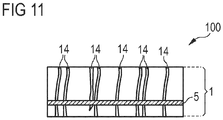
- FIGS 7A and 7B a light-emitting diode chip is shown without intermediate layers.
- the semiconductor layer sequence 1 is grown on the growth substrate 11, either at the interface between the undoped layer 15 or the n-doped layer sequence 4, which according to FIG Figure 7 is formed by a single layer, and compare the growth substrate 11 or also during the growth or during the laser lift-off process within the semiconductor layer sequence 1, cracks and / or holes 14 Figure 7A , When the growth substrate 11 is separated from the semiconductor layer sequence 1, for example by the laser lift-off method, part of the cracks and / or holes 14 is exposed, see Figure 7B ,
- a portion of the cracks and / or holes 14 extends from the side 40 of the n-doped layer sequence 4 to the p-contact 12p.
- These holes and / or cracks 14 make it possible for a liquid chemical such as nitric acid or potassium hydroxide solution to pass through the semiconductor layer sequence 1 to the p-type contact 12p in a later process step, for example to produce a roughening on the n-doped layer sequence 4 arrives, the semiconductor layer sequence 1 thus completely penetrated.
- FIG Figure 8 A modification of the semiconductor chip 100 with the intermediate layer 5 is illustrated, after which the growth substrate 11 is separated from the semiconductor layer sequence 1. In contrast to the drawing, it is also possible for only one of the layers 15, 17 to be present.
- the semiconductor layer sequence 1 according to FIG Figure 8 has cracks and / or holes 14 which run from the side 40 of the n-doped layer sequence 4 to the p-contact 12p and which are exposed by, for example, a laser lifting process on the side 40 facing the separated growth substrate 11.
- the intermediate layer 5 is thus used as a kind of seal or sealing layer for the cracks and / or holes 14. This is made possible in particular by the fact that the intermediate layer 5 and the elevations 50 are formed with AlGaN instead of GaN. Aluminum atoms are less mobile than gallium atoms when growing epitaxially on a surface. This enables the cracks and / or holes 14 to be closed and partially filled.
- the effect of the sealing of cracks and / or holes 14 by the intermediate layer 5 is particularly important when a distance between the roughening 8 or an outer boundary surface of the semiconductor layer sequence 1 and the mirror 16, 16a, 16b is particularly small, as is especially the case with the modifications or exemplary embodiments according to Figures 3 and 6 ,
- FIG. 9 Further modifications or exemplary embodiments of the semiconductor chips 100 are shown in a sectional illustration and in an associated plan view of a radiation passage side with a contact area 18, for example for a bond wire.
- the semiconductor chips 100 each have a plurality of plated-through holes 10 and mirrors 16b, which are not shown in the sectional views, see FIG Figures 3 and 6 ,
- the plated-through holes 10 and mirror 16b thus each extend from the p-type layer sequence 2 to the current spreading layer 7, each of which has a thickness of approximately 1.1 ⁇ m.
- the intermediate layer 5 has a thickness of approximately 60 nm, in accordance with the modification of FIG Figure 9B a thickness of approximately 30 nm.
- the n-doped layer 17 each has a thickness of approximately 1.3 ⁇ m.
- the current spreading layer 7 is located between the two intermediate layers 5a, 5b, each with a thickness of approximately 30 nm. There is therefore at least one intermediate layer 5, 5a, 5b on each side of the current spreading layer 7 facing away from the active zone 3.
- the mirrors 16b show no reduced reflectivity and are therefore not damaged. In particular, more than 50% or more than 80% of the radiation leaves the semiconductor chip 100 through the radiation passage side.
- the intermediate layers 5 are each located between the current spreading layer 7 and the active zone 3. There is therefore no intermediate layer between the mirrors 16b and the radiation passage side.
- the mirrors 16b are exposed to liquid chemicals, for example when roughening is generated on the radiation passage side, and are thereby damaged, which can be seen in a darkening and thus reduced reflectivity of the mirrors 16b.
- the semiconductor layer sequence 1 with the intermediate layer 5 is only shown in simplified form in a sectional view, in particular electrical contacts are not shown.
- the holes and / or cracks 14 in the semiconductor layer sequence 1 are reduced in diameter or, in the region of the intermediate layer 5, completely covered or blocked by the material of the intermediate layer 5.
- the holes and / or cracks 14 are in front of the Intermediate layer 5 is therefore larger than after the intermediate layer 5.
- a direction along which the cracks and / or holes 14 run can be changed by the intermediate layer 5.
- the holes and / or cracks 14 are sealed against liquid chemicals and / or against vapors and / or the diffusion of metals.
- the holes and / or cracks 14 are not eliminated in the crystal lattice of the semiconductor layer sequence 1 by the intermediate layer 5, but continue, seen along the growth direction of the semiconductor layer sequence 1, after the intermediate layer 5. In other words, it is possible that a number of the cracks and / or holes 14 is not or not significantly reduced by the intermediate layer 5. Regardless of the approximately constant number of cracks and / or holes 14 on both sides of the intermediate layer 14, the holes and / or cracks 14 are impermeable to chemicals due to the material of the intermediate layer 5.
Landscapes
- Led Devices (AREA)
Applications Claiming Priority (2)
| Application Number | Priority Date | Filing Date | Title |
|---|---|---|---|
| DE102009060749.8A DE102009060749B4 (de) | 2009-12-30 | 2009-12-30 | Optoelektronischer Halbleiterchip |
| PCT/EP2010/070274 WO2011080144A2 (de) | 2009-12-30 | 2010-12-20 | Optoelektronischer halbleiterchip und verwendung einer auf algan basierenden zwischenschicht |
Publications (2)
| Publication Number | Publication Date |
|---|---|
| EP2519979A2 EP2519979A2 (de) | 2012-11-07 |
| EP2519979B1 true EP2519979B1 (de) | 2019-12-18 |
Family
ID=43640034
Family Applications (1)
| Application Number | Title | Priority Date | Filing Date |
|---|---|---|---|
| EP10798083.1A Active EP2519979B1 (de) | 2009-12-30 | 2010-12-20 | Optoelektronischer halbleiterchip mit zwei auf algan basierenden zwischenschichten |
Country Status (8)
| Country | Link |
|---|---|
| US (1) | US8592840B2 (enExample) |
| EP (1) | EP2519979B1 (enExample) |
| JP (1) | JP2013516749A (enExample) |
| KR (1) | KR101759273B1 (enExample) |
| CN (1) | CN102687289B (enExample) |
| DE (1) | DE102009060749B4 (enExample) |
| TW (1) | TWI442600B (enExample) |
| WO (1) | WO2011080144A2 (enExample) |
Families Citing this family (6)
| Publication number | Priority date | Publication date | Assignee | Title |
|---|---|---|---|---|
| DE102009058796A1 (de) | 2009-12-18 | 2011-06-22 | OSRAM Opto Semiconductors GmbH, 93055 | Optoelektronisches Bauelement und Verfahren zur Herstellung eines optoelektronischen Bauelements |
| US9419182B2 (en) | 2012-01-05 | 2016-08-16 | Micron Technology, Inc. | Solid-state radiation transducer devices having at least partially transparent buried-contact elements, and associated systems and methods |
| CN108615725A (zh) | 2012-07-11 | 2018-10-02 | 亮锐控股有限公司 | 降低或者消除ⅲ-氮化物结构中的纳米管缺陷 |
| DE102012111245A1 (de) * | 2012-11-21 | 2014-05-22 | Osram Opto Semiconductors Gmbh | Verfahren zur Herstellung eines Anschlussbereichs eines optoelektronischen Halbleiterchips |
| DE102013104192A1 (de) | 2013-04-25 | 2014-10-30 | Osram Opto Semiconductors Gmbh | Halbleiterbauelement mit einer Zwischenschicht |
| DE102018126936A1 (de) * | 2018-10-29 | 2020-04-30 | Osram Opto Semiconductors Gmbh | Verfahren zur Herstellung von optoelektronischen Halbleiterbauteilen |
Citations (5)
| Publication number | Priority date | Publication date | Assignee | Title |
|---|---|---|---|---|
| US6121638A (en) * | 1995-09-12 | 2000-09-19 | Kabushiki Kaisha Toshiba | Multi-layer structured nitride-based semiconductor devices |
| US20030230754A1 (en) * | 2002-06-13 | 2003-12-18 | Steigerwald Daniel A. | Contacting scheme for large and small area semiconductor light emitting flip chip devices |
| WO2005036658A1 (en) * | 2003-10-14 | 2005-04-21 | Showa Denko K.K. | Group-iii nitride semiconductor device |
| DE102008011848A1 (de) * | 2008-02-29 | 2009-09-03 | Osram Opto Semiconductors Gmbh | Optoelektronischer Halbleiterkörper und Verfahren zur Herstellung eines solchen |
| US20090283787A1 (en) * | 2007-11-14 | 2009-11-19 | Matthew Donofrio | Semiconductor light emitting diodes having reflective structures and methods of fabricating same |
Family Cites Families (20)
| Publication number | Priority date | Publication date | Assignee | Title |
|---|---|---|---|---|
| US5903017A (en) * | 1996-02-26 | 1999-05-11 | Kabushiki Kaisha Toshiba | Compound semiconductor device formed of nitrogen-containing gallium compound such as GaN, AlGaN or InGaN |
| DE69835216T2 (de) * | 1997-07-25 | 2007-05-31 | Nichia Corp., Anan | Halbleitervorrichtung aus einer nitridverbindung |
| JP4166885B2 (ja) * | 1998-05-18 | 2008-10-15 | 富士通株式会社 | 光半導体装置およびその製造方法 |
| JP3786544B2 (ja) * | 1999-06-10 | 2006-06-14 | パイオニア株式会社 | 窒化物半導体素子の製造方法及びかかる方法により製造された素子 |
| DE10042947A1 (de) * | 2000-08-31 | 2002-03-21 | Osram Opto Semiconductors Gmbh | Strahlungsemittierendes Halbleiterbauelement auf GaN-Basis |
| US6504183B1 (en) | 2000-09-08 | 2003-01-07 | United Epitaxy Company | Epitaxial growth of nitride semiconductor device |
| DE10056475B4 (de) * | 2000-11-15 | 2010-10-07 | Osram Opto Semiconductors Gmbh | Strahlungsemittierendes Halbleiterbauelement auf GaN-Basis mit verbesserter p-Leitfähigkeit und Verfahren zu dessen Herstellung |
| KR100580623B1 (ko) * | 2003-08-04 | 2006-05-16 | 삼성전자주식회사 | 초격자 구조의 반도체층을 갖는 반도체 소자 및 그 제조방법 |
| JP4423969B2 (ja) * | 2003-12-25 | 2010-03-03 | 日亜化学工業株式会社 | 窒化物半導体積層基板およびそれを用いた窒化物半導体デバイス、窒化物半導体レーザ素子 |
| KR101386192B1 (ko) | 2004-01-26 | 2014-04-17 | 오스람 옵토 세미컨덕터스 게엠베하 | 전류 분산 구조물을 갖는 박막 led |
| DE102005003460A1 (de) * | 2004-01-26 | 2005-10-13 | Osram Opto Semiconductors Gmbh | Dünnfilm-LED mit einer Stromaufweitungsstruktur |
| WO2005106972A1 (de) * | 2004-04-29 | 2005-11-10 | Osram Opto Semiconductors Gmbh | Verfahren zum herstellen eines strahlungsemittierenden halbleiterchips |
| JP2007201195A (ja) | 2006-01-26 | 2007-08-09 | Sumitomo Electric Ind Ltd | 窒化物半導体発光素子 |
| JPWO2007129773A1 (ja) | 2006-05-10 | 2009-09-17 | 昭和電工株式会社 | Iii族窒化物化合物半導体積層構造体 |
| EP1883141B1 (de) | 2006-07-27 | 2017-05-24 | OSRAM Opto Semiconductors GmbH | LD oder LED mit Übergitter-Mantelschicht |
| DE102006046237A1 (de) * | 2006-07-27 | 2008-01-31 | Osram Opto Semiconductors Gmbh | Halbleiter-Schichtstruktur mit Übergitter |
| DE102007046027A1 (de) | 2007-09-26 | 2009-04-02 | Osram Opto Semiconductors Gmbh | Optoelektronischer Halbleiterchip mit einer Mehrfachquantentopfstruktur |
| DE102007057241A1 (de) | 2007-11-28 | 2009-06-04 | Osram Opto Semiconductors Gmbh | Verfahren zur Herstellung eines Schichtenstapels auf einem kristallinen Substrat und Anordnung umfassend einen auf einem Substrat angeordneten Schichtenstapel |
| DE102008032318A1 (de) | 2008-03-31 | 2009-10-01 | Osram Opto Semiconductors Gmbh | Optoelektronischer Halbleiterchip und Verfahren zur Herstellung eines solchen |
| KR101055090B1 (ko) * | 2009-03-02 | 2011-08-08 | 엘지이노텍 주식회사 | 반도체 발광소자 및 그 제조방법 |
-
2009
- 2009-12-30 DE DE102009060749.8A patent/DE102009060749B4/de active Active
-
2010
- 2010-12-20 US US13/519,345 patent/US8592840B2/en active Active
- 2010-12-20 WO PCT/EP2010/070274 patent/WO2011080144A2/de not_active Ceased
- 2010-12-20 JP JP2012546412A patent/JP2013516749A/ja active Pending
- 2010-12-20 CN CN201080060178.5A patent/CN102687289B/zh active Active
- 2010-12-20 EP EP10798083.1A patent/EP2519979B1/de active Active
- 2010-12-20 KR KR1020127020129A patent/KR101759273B1/ko active Active
- 2010-12-28 TW TW099146210A patent/TWI442600B/zh active
Patent Citations (5)
| Publication number | Priority date | Publication date | Assignee | Title |
|---|---|---|---|---|
| US6121638A (en) * | 1995-09-12 | 2000-09-19 | Kabushiki Kaisha Toshiba | Multi-layer structured nitride-based semiconductor devices |
| US20030230754A1 (en) * | 2002-06-13 | 2003-12-18 | Steigerwald Daniel A. | Contacting scheme for large and small area semiconductor light emitting flip chip devices |
| WO2005036658A1 (en) * | 2003-10-14 | 2005-04-21 | Showa Denko K.K. | Group-iii nitride semiconductor device |
| US20090283787A1 (en) * | 2007-11-14 | 2009-11-19 | Matthew Donofrio | Semiconductor light emitting diodes having reflective structures and methods of fabricating same |
| DE102008011848A1 (de) * | 2008-02-29 | 2009-09-03 | Osram Opto Semiconductors Gmbh | Optoelektronischer Halbleiterkörper und Verfahren zur Herstellung eines solchen |
Also Published As
| Publication number | Publication date |
|---|---|
| KR101759273B1 (ko) | 2017-07-18 |
| CN102687289A (zh) | 2012-09-19 |
| US8592840B2 (en) | 2013-11-26 |
| US20120313138A1 (en) | 2012-12-13 |
| DE102009060749A1 (de) | 2011-07-07 |
| EP2519979A2 (de) | 2012-11-07 |
| CN102687289B (zh) | 2016-08-03 |
| WO2011080144A2 (de) | 2011-07-07 |
| KR20120094528A (ko) | 2012-08-24 |
| TWI442600B (zh) | 2014-06-21 |
| WO2011080144A3 (de) | 2011-12-22 |
| TW201135976A (en) | 2011-10-16 |
| DE102009060749B4 (de) | 2021-12-30 |
| JP2013516749A (ja) | 2013-05-13 |
Similar Documents
| Publication | Publication Date | Title |
|---|---|---|
| DE112006001084B4 (de) | Licht emittierende Bauelemente mit aktiven Schichten, die sich in geöffnete Grübchen erstrecken | |
| DE112004002809B9 (de) | Verfahren zum Herstellen eines strahlungsemittierenden Halbleiterchips und durch dieses Verfahren hergestellter Halbleiterchip | |
| DE102012101718B4 (de) | Optoelektronischer Halbleiterchip | |
| DE69835216T2 (de) | Halbleitervorrichtung aus einer nitridverbindung | |
| EP2208240B1 (de) | Optoelektronischer halbleiterchip mit einer mehrfachquantentopfstruktur | |
| EP1709694B1 (de) | Dünnfilm-led mit einer stromaufweitungsstruktur | |
| EP2193550B1 (de) | Strahlungsemittierender halbleiterkörper | |
| WO2014053445A1 (de) | Verfahren zur herstellung eines leuchtdioden-displays und leuchtdioden-display | |
| EP2519979B1 (de) | Optoelektronischer halbleiterchip mit zwei auf algan basierenden zwischenschichten | |
| DE102007056970A1 (de) | Halbleiterelemente mit geringen TDs (Threading Dislocations) und verbesserter Lichtextraktion sowie Verfahren zum Herstellen derselben | |
| DE112007000223T5 (de) | Nitridhalbleiterlichtemissionselement mit einer verbesserten Lichtentnahmeeffizienz | |
| WO2018122103A1 (de) | Halbleiterlaserdiode | |
| DE102005052357A1 (de) | Verfahren zum lateralen Zertrennen eines Halbleiterwafers und optoelektronisches Bauelement | |
| WO2012049031A1 (de) | Verfahren zur herstellung einer halbleiterschichtenfolge, strahlungsemittierender halbleiterchip und optoelektronisches bauteil | |
| DE102009059887A1 (de) | Optoelektronischer Halbleiterchip | |
| EP1299909B1 (de) | LUMINESZENZDIODENCHIP AUF DER BASIS VON InGaN UND VERFAHREN ZU DESSEN HERSTELLUNG | |
| DE102007057756B4 (de) | Verfahren zur Herstellung eines optoelektronischen Halbleiterkörpers | |
| WO2017060158A1 (de) | Verfahren zur herstellung eines halbleiterchips und halbleiterchip | |
| DE102016124860A1 (de) | Optoelektronischer Halbleiterchip und Verfahren zur Herstellung eines optoelektronischen Halbleiterchips | |
| WO2020038743A1 (de) | Optoelektronisches halbleiterbauelement mit einer halbleiterkontaktschicht und verfahren zur herstellung des optoelektronischen halbleiterbauelements | |
| DE102005003460A1 (de) | Dünnfilm-LED mit einer Stromaufweitungsstruktur | |
| WO2021175635A1 (de) | Strahlungsemittierender halbleiterkörper und dessen verfahren zur herstellung | |
| DE10244447B4 (de) | Strahlungsemittierendes Halbleiterbauelement mit vertikaler Emissionsrichtung und Herstellungsverfahren dafür | |
| WO2017021301A1 (de) | Verfahren zur herstellung eines nitrid-halbleiterbauelements und nitrid-halbleiterbauelement | |
| DE102017105397A1 (de) | Verfahren zur Herstellung von Leuchtdioden und Leuchtdiode |
Legal Events
| Date | Code | Title | Description |
|---|---|---|---|
| PUAI | Public reference made under article 153(3) epc to a published international application that has entered the european phase |
Free format text: ORIGINAL CODE: 0009012 |
|
| 17P | Request for examination filed |
Effective date: 20120411 |
|
| AK | Designated contracting states |
Kind code of ref document: A2 Designated state(s): AL AT BE BG CH CY CZ DE DK EE ES FI FR GB GR HR HU IE IS IT LI LT LU LV MC MK MT NL NO PL PT RO RS SE SI SK SM TR |
|
| RIN1 | Information on inventor provided before grant (corrected) |
Inventor name: LUGAUER, HANS-JUERGEN Inventor name: TAKI, TETSUYA Inventor name: WALTER, ALEXANDER Inventor name: GMEINWIESER, NIKOLAUS Inventor name: MEYER, TOBIAS Inventor name: PETER, MATTHIAS |
|
| RIN1 | Information on inventor provided before grant (corrected) |
Inventor name: GMEINWIESER, NIKOLAUS Inventor name: WALTER, ALEXANDER Inventor name: LUGAUER, HANS-JUERGEN Inventor name: PETER, MATTHIAS Inventor name: MEYER, TOBIAS Inventor name: TAKI, TETSUYA |
|
| DAX | Request for extension of the european patent (deleted) | ||
| STAA | Information on the status of an ep patent application or granted ep patent |
Free format text: STATUS: EXAMINATION IS IN PROGRESS |
|
| PUAG | Search results despatched under rule 164(2) epc together with communication from examining division |
Free format text: ORIGINAL CODE: 0009017 |
|
| 17Q | First examination report despatched |
Effective date: 20181205 |
|
| 17Q | First examination report despatched |
Effective date: 20190108 |
|
| B565 | Issuance of search results under rule 164(2) epc |
Effective date: 20190108 |
|
| RIC1 | Information provided on ipc code assigned before grant |
Ipc: H01L 33/22 20100101ALN20190103BHEP Ipc: H01L 33/00 20100101AFI20190103BHEP Ipc: H01L 33/12 20100101ALN20190103BHEP Ipc: H01L 33/02 20100101ALI20190103BHEP Ipc: H01L 33/32 20100101ALI20190103BHEP Ipc: H01L 33/16 20100101ALN20190103BHEP |
|
| RIC1 | Information provided on ipc code assigned before grant |
Ipc: H01L 33/16 20100101ALN20190524BHEP Ipc: H01L 33/14 20100101ALN20190524BHEP Ipc: H01L 33/12 20100101ALN20190524BHEP Ipc: H01L 33/00 20100101AFI20190524BHEP Ipc: H01L 33/32 20100101ALI20190524BHEP Ipc: H01L 33/38 20100101ALI20190524BHEP Ipc: H01L 33/22 20100101ALN20190524BHEP |
|
| GRAP | Despatch of communication of intention to grant a patent |
Free format text: ORIGINAL CODE: EPIDOSNIGR1 |
|
| STAA | Information on the status of an ep patent application or granted ep patent |
Free format text: STATUS: GRANT OF PATENT IS INTENDED |
|
| RIC1 | Information provided on ipc code assigned before grant |
Ipc: H01L 33/32 20100101ALI20190704BHEP Ipc: H01L 33/16 20100101ALN20190704BHEP Ipc: H01L 33/00 20100101AFI20190704BHEP Ipc: H01L 33/12 20100101ALN20190704BHEP Ipc: H01L 33/22 20100101ALN20190704BHEP Ipc: H01L 33/14 20100101ALN20190704BHEP Ipc: H01L 33/38 20100101ALI20190704BHEP |
|
| INTG | Intention to grant announced |
Effective date: 20190725 |
|
| RAP1 | Party data changed (applicant data changed or rights of an application transferred) |
Owner name: OSRAM OPTO SEMICONDUCTORS GMBH |
|
| GRAS | Grant fee paid |
Free format text: ORIGINAL CODE: EPIDOSNIGR3 |
|
| GRAA | (expected) grant |
Free format text: ORIGINAL CODE: 0009210 |
|
| STAA | Information on the status of an ep patent application or granted ep patent |
Free format text: STATUS: THE PATENT HAS BEEN GRANTED |
|
| AK | Designated contracting states |
Kind code of ref document: B1 Designated state(s): AL AT BE BG CH CY CZ DE DK EE ES FI FR GB GR HR HU IE IS IT LI LT LU LV MC MK MT NL NO PL PT RO RS SE SI SK SM TR |
|
| REG | Reference to a national code |
Ref country code: GB Ref legal event code: FG4D Free format text: NOT ENGLISH |
|
| REG | Reference to a national code |
Ref country code: CH Ref legal event code: EP |
|
| REG | Reference to a national code |
Ref country code: IE Ref legal event code: FG4D Free format text: LANGUAGE OF EP DOCUMENT: GERMAN |
|
| REG | Reference to a national code |
Ref country code: DE Ref legal event code: R096 Ref document number: 502010016421 Country of ref document: DE |
|
| REG | Reference to a national code |
Ref country code: AT Ref legal event code: REF Ref document number: 1215549 Country of ref document: AT Kind code of ref document: T Effective date: 20200115 |
|
| REG | Reference to a national code |
Ref country code: NL Ref legal event code: MP Effective date: 20191218 |
|
| PG25 | Lapsed in a contracting state [announced via postgrant information from national office to epo] |
Ref country code: LT Free format text: LAPSE BECAUSE OF FAILURE TO SUBMIT A TRANSLATION OF THE DESCRIPTION OR TO PAY THE FEE WITHIN THE PRESCRIBED TIME-LIMIT Effective date: 20191218 Ref country code: GR Free format text: LAPSE BECAUSE OF FAILURE TO SUBMIT A TRANSLATION OF THE DESCRIPTION OR TO PAY THE FEE WITHIN THE PRESCRIBED TIME-LIMIT Effective date: 20200319 Ref country code: NO Free format text: LAPSE BECAUSE OF FAILURE TO SUBMIT A TRANSLATION OF THE DESCRIPTION OR TO PAY THE FEE WITHIN THE PRESCRIBED TIME-LIMIT Effective date: 20200318 Ref country code: BG Free format text: LAPSE BECAUSE OF FAILURE TO SUBMIT A TRANSLATION OF THE DESCRIPTION OR TO PAY THE FEE WITHIN THE PRESCRIBED TIME-LIMIT Effective date: 20200318 Ref country code: FI Free format text: LAPSE BECAUSE OF FAILURE TO SUBMIT A TRANSLATION OF THE DESCRIPTION OR TO PAY THE FEE WITHIN THE PRESCRIBED TIME-LIMIT Effective date: 20191218 Ref country code: SE Free format text: LAPSE BECAUSE OF FAILURE TO SUBMIT A TRANSLATION OF THE DESCRIPTION OR TO PAY THE FEE WITHIN THE PRESCRIBED TIME-LIMIT Effective date: 20191218 Ref country code: LV Free format text: LAPSE BECAUSE OF FAILURE TO SUBMIT A TRANSLATION OF THE DESCRIPTION OR TO PAY THE FEE WITHIN THE PRESCRIBED TIME-LIMIT Effective date: 20191218 |
|
| REG | Reference to a national code |
Ref country code: LT Ref legal event code: MG4D |
|
| PG25 | Lapsed in a contracting state [announced via postgrant information from national office to epo] |
Ref country code: RS Free format text: LAPSE BECAUSE OF FAILURE TO SUBMIT A TRANSLATION OF THE DESCRIPTION OR TO PAY THE FEE WITHIN THE PRESCRIBED TIME-LIMIT Effective date: 20191218 Ref country code: HR Free format text: LAPSE BECAUSE OF FAILURE TO SUBMIT A TRANSLATION OF THE DESCRIPTION OR TO PAY THE FEE WITHIN THE PRESCRIBED TIME-LIMIT Effective date: 20191218 |
|
| PG25 | Lapsed in a contracting state [announced via postgrant information from national office to epo] |
Ref country code: AL Free format text: LAPSE BECAUSE OF FAILURE TO SUBMIT A TRANSLATION OF THE DESCRIPTION OR TO PAY THE FEE WITHIN THE PRESCRIBED TIME-LIMIT Effective date: 20191218 |
|
| PG25 | Lapsed in a contracting state [announced via postgrant information from national office to epo] |
Ref country code: PT Free format text: LAPSE BECAUSE OF FAILURE TO SUBMIT A TRANSLATION OF THE DESCRIPTION OR TO PAY THE FEE WITHIN THE PRESCRIBED TIME-LIMIT Effective date: 20200513 Ref country code: CZ Free format text: LAPSE BECAUSE OF FAILURE TO SUBMIT A TRANSLATION OF THE DESCRIPTION OR TO PAY THE FEE WITHIN THE PRESCRIBED TIME-LIMIT Effective date: 20191218 Ref country code: NL Free format text: LAPSE BECAUSE OF FAILURE TO SUBMIT A TRANSLATION OF THE DESCRIPTION OR TO PAY THE FEE WITHIN THE PRESCRIBED TIME-LIMIT Effective date: 20191218 Ref country code: RO Free format text: LAPSE BECAUSE OF FAILURE TO SUBMIT A TRANSLATION OF THE DESCRIPTION OR TO PAY THE FEE WITHIN THE PRESCRIBED TIME-LIMIT Effective date: 20191218 Ref country code: EE Free format text: LAPSE BECAUSE OF FAILURE TO SUBMIT A TRANSLATION OF THE DESCRIPTION OR TO PAY THE FEE WITHIN THE PRESCRIBED TIME-LIMIT Effective date: 20191218 |
|
| REG | Reference to a national code |
Ref country code: CH Ref legal event code: PL |
|
| REG | Reference to a national code |
Ref country code: BE Ref legal event code: MM Effective date: 20191231 |
|
| PG25 | Lapsed in a contracting state [announced via postgrant information from national office to epo] |
Ref country code: IS Free format text: LAPSE BECAUSE OF FAILURE TO SUBMIT A TRANSLATION OF THE DESCRIPTION OR TO PAY THE FEE WITHIN THE PRESCRIBED TIME-LIMIT Effective date: 20200418 Ref country code: SK Free format text: LAPSE BECAUSE OF FAILURE TO SUBMIT A TRANSLATION OF THE DESCRIPTION OR TO PAY THE FEE WITHIN THE PRESCRIBED TIME-LIMIT Effective date: 20191218 Ref country code: SM Free format text: LAPSE BECAUSE OF FAILURE TO SUBMIT A TRANSLATION OF THE DESCRIPTION OR TO PAY THE FEE WITHIN THE PRESCRIBED TIME-LIMIT Effective date: 20191218 |
|
| REG | Reference to a national code |
Ref country code: DE Ref legal event code: R097 Ref document number: 502010016421 Country of ref document: DE |
|
| PG25 | Lapsed in a contracting state [announced via postgrant information from national office to epo] |
Ref country code: MC Free format text: LAPSE BECAUSE OF FAILURE TO SUBMIT A TRANSLATION OF THE DESCRIPTION OR TO PAY THE FEE WITHIN THE PRESCRIBED TIME-LIMIT Effective date: 20191218 |
|
| PLBE | No opposition filed within time limit |
Free format text: ORIGINAL CODE: 0009261 |
|
| STAA | Information on the status of an ep patent application or granted ep patent |
Free format text: STATUS: NO OPPOSITION FILED WITHIN TIME LIMIT |
|
| PG25 | Lapsed in a contracting state [announced via postgrant information from national office to epo] |
Ref country code: IE Free format text: LAPSE BECAUSE OF NON-PAYMENT OF DUE FEES Effective date: 20191220 Ref country code: ES Free format text: LAPSE BECAUSE OF FAILURE TO SUBMIT A TRANSLATION OF THE DESCRIPTION OR TO PAY THE FEE WITHIN THE PRESCRIBED TIME-LIMIT Effective date: 20191218 Ref country code: DK Free format text: LAPSE BECAUSE OF FAILURE TO SUBMIT A TRANSLATION OF THE DESCRIPTION OR TO PAY THE FEE WITHIN THE PRESCRIBED TIME-LIMIT Effective date: 20191218 Ref country code: LU Free format text: LAPSE BECAUSE OF NON-PAYMENT OF DUE FEES Effective date: 20191220 |
|
| 26N | No opposition filed |
Effective date: 20200921 |
|
| PG25 | Lapsed in a contracting state [announced via postgrant information from national office to epo] |
Ref country code: LI Free format text: LAPSE BECAUSE OF NON-PAYMENT OF DUE FEES Effective date: 20191231 Ref country code: CH Free format text: LAPSE BECAUSE OF NON-PAYMENT OF DUE FEES Effective date: 20191231 Ref country code: SI Free format text: LAPSE BECAUSE OF FAILURE TO SUBMIT A TRANSLATION OF THE DESCRIPTION OR TO PAY THE FEE WITHIN THE PRESCRIBED TIME-LIMIT Effective date: 20191218 Ref country code: BE Free format text: LAPSE BECAUSE OF NON-PAYMENT OF DUE FEES Effective date: 20191231 |
|
| PG25 | Lapsed in a contracting state [announced via postgrant information from national office to epo] |
Ref country code: FR Free format text: LAPSE BECAUSE OF NON-PAYMENT OF DUE FEES Effective date: 20200218 Ref country code: IT Free format text: LAPSE BECAUSE OF FAILURE TO SUBMIT A TRANSLATION OF THE DESCRIPTION OR TO PAY THE FEE WITHIN THE PRESCRIBED TIME-LIMIT Effective date: 20191218 |
|
| REG | Reference to a national code |
Ref country code: AT Ref legal event code: MM01 Ref document number: 1215549 Country of ref document: AT Kind code of ref document: T Effective date: 20191220 |
|
| PG25 | Lapsed in a contracting state [announced via postgrant information from national office to epo] |
Ref country code: PL Free format text: LAPSE BECAUSE OF FAILURE TO SUBMIT A TRANSLATION OF THE DESCRIPTION OR TO PAY THE FEE WITHIN THE PRESCRIBED TIME-LIMIT Effective date: 20191218 |
|
| GBPC | Gb: european patent ceased through non-payment of renewal fee |
Effective date: 20200318 |
|
| PG25 | Lapsed in a contracting state [announced via postgrant information from national office to epo] |
Ref country code: GB Free format text: LAPSE BECAUSE OF NON-PAYMENT OF DUE FEES Effective date: 20200318 |
|
| PG25 | Lapsed in a contracting state [announced via postgrant information from national office to epo] |
Ref country code: CY Free format text: LAPSE BECAUSE OF FAILURE TO SUBMIT A TRANSLATION OF THE DESCRIPTION OR TO PAY THE FEE WITHIN THE PRESCRIBED TIME-LIMIT Effective date: 20191218 Ref country code: AT Free format text: LAPSE BECAUSE OF NON-PAYMENT OF DUE FEES Effective date: 20191220 |
|
| PG25 | Lapsed in a contracting state [announced via postgrant information from national office to epo] |
Ref country code: HU Free format text: LAPSE BECAUSE OF FAILURE TO SUBMIT A TRANSLATION OF THE DESCRIPTION OR TO PAY THE FEE WITHIN THE PRESCRIBED TIME-LIMIT; INVALID AB INITIO Effective date: 20101220 Ref country code: MT Free format text: LAPSE BECAUSE OF FAILURE TO SUBMIT A TRANSLATION OF THE DESCRIPTION OR TO PAY THE FEE WITHIN THE PRESCRIBED TIME-LIMIT Effective date: 20191218 |
|
| PG25 | Lapsed in a contracting state [announced via postgrant information from national office to epo] |
Ref country code: TR Free format text: LAPSE BECAUSE OF FAILURE TO SUBMIT A TRANSLATION OF THE DESCRIPTION OR TO PAY THE FEE WITHIN THE PRESCRIBED TIME-LIMIT Effective date: 20191218 |
|
| PG25 | Lapsed in a contracting state [announced via postgrant information from national office to epo] |
Ref country code: MK Free format text: LAPSE BECAUSE OF FAILURE TO SUBMIT A TRANSLATION OF THE DESCRIPTION OR TO PAY THE FEE WITHIN THE PRESCRIBED TIME-LIMIT Effective date: 20191218 |
|
| P01 | Opt-out of the competence of the unified patent court (upc) registered |
Effective date: 20230825 |
|
| REG | Reference to a national code |
Ref country code: DE Ref legal event code: R079 Ref document number: 502010016421 Country of ref document: DE Free format text: PREVIOUS MAIN CLASS: H01L0033000000 Ipc: H10H0020000000 |
|
| PGFP | Annual fee paid to national office [announced via postgrant information from national office to epo] |
Ref country code: DE Payment date: 20241210 Year of fee payment: 15 |