JP2013516749A - オプトエレクトロニクス半導体チップおよびAlGaNをベースとする中間層の使用 - Google Patents
オプトエレクトロニクス半導体チップおよびAlGaNをベースとする中間層の使用 Download PDFInfo
- Publication number
- JP2013516749A JP2013516749A JP2012546412A JP2012546412A JP2013516749A JP 2013516749 A JP2013516749 A JP 2013516749A JP 2012546412 A JP2012546412 A JP 2012546412A JP 2012546412 A JP2012546412 A JP 2012546412A JP 2013516749 A JP2013516749 A JP 2013516749A
- Authority
- JP
- Japan
- Prior art keywords
- intermediate layer
- layer
- semiconductor chip
- hole
- optoelectronic semiconductor
- Prior art date
- Legal status (The legal status is an assumption and is not a legal conclusion. Google has not performed a legal analysis and makes no representation as to the accuracy of the status listed.)
- Pending
Links
Images


Classifications
-
- H—ELECTRICITY
- H01—ELECTRIC ELEMENTS
- H01L—SEMICONDUCTOR DEVICES NOT COVERED BY CLASS H10
- H01L33/00—Semiconductor devices with at least one potential-jump barrier or surface barrier specially adapted for light emission; Processes or apparatus specially adapted for the manufacture or treatment thereof or of parts thereof; Details thereof
- H01L33/005—Processes
- H01L33/0062—Processes for devices with an active region comprising only III-V compounds
- H01L33/0066—Processes for devices with an active region comprising only III-V compounds with a substrate not being a III-V compound
- H01L33/007—Processes for devices with an active region comprising only III-V compounds with a substrate not being a III-V compound comprising nitride compounds
-
- H—ELECTRICITY
- H01—ELECTRIC ELEMENTS
- H01L—SEMICONDUCTOR DEVICES NOT COVERED BY CLASS H10
- H01L33/00—Semiconductor devices with at least one potential-jump barrier or surface barrier specially adapted for light emission; Processes or apparatus specially adapted for the manufacture or treatment thereof or of parts thereof; Details thereof
- H01L33/02—Semiconductor devices with at least one potential-jump barrier or surface barrier specially adapted for light emission; Processes or apparatus specially adapted for the manufacture or treatment thereof or of parts thereof; Details thereof characterised by the semiconductor bodies
- H01L33/025—Physical imperfections, e.g. particular concentration or distribution of impurities
-
- H—ELECTRICITY
- H01—ELECTRIC ELEMENTS
- H01L—SEMICONDUCTOR DEVICES NOT COVERED BY CLASS H10
- H01L33/00—Semiconductor devices with at least one potential-jump barrier or surface barrier specially adapted for light emission; Processes or apparatus specially adapted for the manufacture or treatment thereof or of parts thereof; Details thereof
- H01L33/02—Semiconductor devices with at least one potential-jump barrier or surface barrier specially adapted for light emission; Processes or apparatus specially adapted for the manufacture or treatment thereof or of parts thereof; Details thereof characterised by the semiconductor bodies
- H01L33/26—Materials of the light emitting region
- H01L33/30—Materials of the light emitting region containing only elements of group III and group V of the periodic system
- H01L33/32—Materials of the light emitting region containing only elements of group III and group V of the periodic system containing nitrogen
-
- H—ELECTRICITY
- H01—ELECTRIC ELEMENTS
- H01L—SEMICONDUCTOR DEVICES NOT COVERED BY CLASS H10
- H01L2924/00—Indexing scheme for arrangements or methods for connecting or disconnecting semiconductor or solid-state bodies as covered by H01L24/00
- H01L2924/0001—Technical content checked by a classifier
- H01L2924/0002—Not covered by any one of groups H01L24/00, H01L24/00 and H01L2224/00
-
- H—ELECTRICITY
- H01—ELECTRIC ELEMENTS
- H01L—SEMICONDUCTOR DEVICES NOT COVERED BY CLASS H10
- H01L33/00—Semiconductor devices with at least one potential-jump barrier or surface barrier specially adapted for light emission; Processes or apparatus specially adapted for the manufacture or treatment thereof or of parts thereof; Details thereof
- H01L33/005—Processes
- H01L33/0093—Wafer bonding; Removal of the growth substrate
-
- H—ELECTRICITY
- H01—ELECTRIC ELEMENTS
- H01L—SEMICONDUCTOR DEVICES NOT COVERED BY CLASS H10
- H01L33/00—Semiconductor devices with at least one potential-jump barrier or surface barrier specially adapted for light emission; Processes or apparatus specially adapted for the manufacture or treatment thereof or of parts thereof; Details thereof
- H01L33/02—Semiconductor devices with at least one potential-jump barrier or surface barrier specially adapted for light emission; Processes or apparatus specially adapted for the manufacture or treatment thereof or of parts thereof; Details thereof characterised by the semiconductor bodies
- H01L33/12—Semiconductor devices with at least one potential-jump barrier or surface barrier specially adapted for light emission; Processes or apparatus specially adapted for the manufacture or treatment thereof or of parts thereof; Details thereof characterised by the semiconductor bodies with a stress relaxation structure, e.g. buffer layer
-
- H—ELECTRICITY
- H01—ELECTRIC ELEMENTS
- H01L—SEMICONDUCTOR DEVICES NOT COVERED BY CLASS H10
- H01L33/00—Semiconductor devices with at least one potential-jump barrier or surface barrier specially adapted for light emission; Processes or apparatus specially adapted for the manufacture or treatment thereof or of parts thereof; Details thereof
- H01L33/02—Semiconductor devices with at least one potential-jump barrier or surface barrier specially adapted for light emission; Processes or apparatus specially adapted for the manufacture or treatment thereof or of parts thereof; Details thereof characterised by the semiconductor bodies
- H01L33/16—Semiconductor devices with at least one potential-jump barrier or surface barrier specially adapted for light emission; Processes or apparatus specially adapted for the manufacture or treatment thereof or of parts thereof; Details thereof characterised by the semiconductor bodies with a particular crystal structure or orientation, e.g. polycrystalline, amorphous or porous
-
- H—ELECTRICITY
- H01—ELECTRIC ELEMENTS
- H01L—SEMICONDUCTOR DEVICES NOT COVERED BY CLASS H10
- H01L33/00—Semiconductor devices with at least one potential-jump barrier or surface barrier specially adapted for light emission; Processes or apparatus specially adapted for the manufacture or treatment thereof or of parts thereof; Details thereof
- H01L33/02—Semiconductor devices with at least one potential-jump barrier or surface barrier specially adapted for light emission; Processes or apparatus specially adapted for the manufacture or treatment thereof or of parts thereof; Details thereof characterised by the semiconductor bodies
- H01L33/20—Semiconductor devices with at least one potential-jump barrier or surface barrier specially adapted for light emission; Processes or apparatus specially adapted for the manufacture or treatment thereof or of parts thereof; Details thereof characterised by the semiconductor bodies with a particular shape, e.g. curved or truncated substrate
- H01L33/22—Roughened surfaces, e.g. at the interface between epitaxial layers
Abstract
Description
本特許出願は、独国特許出願第102009060749.8号の優先権を主張し、この文書の開示内容は参照によって本出願に組み込まれている。
Claims (14)
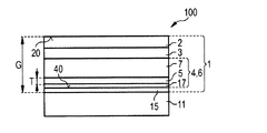
- GaN、InGaN、AlGaN、InAlGaNのうちの少なくとも1種類をベースとする、エピタキシャル成長した半導体積層体(1)、を備えたオプトエレクトロニクス半導体チップ(100)であって、前記半導体積層体(1)が、
− p型にドープされた積層体(2)と、
− n型にドープされた積層体(4)と、
− 電磁放射を生成する目的で設けられている活性ゾーン(3)であって、前記p型にドープされた積層体(2)と前記n型にドープされた積層体(4)との間に位置している、活性ゾーン(3)と、
− AlxGa1−xN(0<x≦1))をベースとする少なくとも1層の中間層(5)であって、前記活性ゾーン(3)を基準として前記n型にドープされた積層体(4)と同じ側に位置している、中間層(5)と、
を備えており、
以下の関係、すなわち、
− 前記中間層(5)が、前記半導体積層体(1)の層のうち前記中間層(5)に隣接する層(4,7,15,17)、における割れ(14)もしくは穴(14)またはその両方の中に延びる突出部(50)、を有し、前記突出部(50)が、前記割れ(14)もしくは前記穴(14)またはその両方の境界領域に少なくとも部分的に直接接触しており、前記割れ(14)もしくは前記穴(14)またはその両方の少なくとも一部またはすべてが、前記中間層(5)によって完全に覆われている、もしくは、
− 前記割れ(14)もしくは前記穴(14)またはその両方の大きさが、前記半導体積層体(1)の成長方向に沿って、前記中間層(5)によって減少し、前記割れ(14)もしくは前記穴(14)またはその両方の少なくとも一部が、前記中間層(5)の両側に延びている、
の少なくとも一方があてはまる、
オプトエレクトロニクス半導体チップ(100)。 - 特に液体に対する、前記中間層(5)の固有の薬剤浸透性が、前記半導体積層体(1)の層のうち前記中間層(5)に隣接する層(4,7,15,17)、におけるよりも小さい、もしくは、
前記中間層(5)が薬液に対して不浸透性である、
またはその両方である、
請求項1に記載のオプトエレクトロニクス半導体チップ(100)。 - 前記中間層(5)、または複数の前記中間層(5)のうちの1層のドーパント濃度が、4×10¹⁸/cm3〜5×1019/cm3の範囲内(両端値を含む)であり、ドーパントがSiである、
請求項1または請求項2に記載のオプトエレクトロニクス半導体チップ(100)。 - 前記中間層(5)、または複数の前記中間層(5)のうちの1層が、ドープされていない、
請求項1から請求項3のいずれかに記載のオプトエレクトロニクス半導体チップ(100)。 - 0.03≦x≦0.5が成り立ち、
1層または2層の前記中間層(5)を備えている、
請求項1から請求項4のいずれかに記載のオプトエレクトロニクス半導体チップ(100)。 - 前記中間層(5)が、15nm〜250nmの範囲内(両端値を含む)の厚さ(T)を有する、
請求項1から請求項5のいずれかに記載のオプトエレクトロニクス半導体チップ(100)。 - 前記中間層(5)、または複数の前記中間層(5)のうちの少なくとも1層が、中断のない連続的な層である、
請求項1から請求項6のいずれかに記載のオプトエレクトロニクス半導体チップ(100)。 - 前記n型にドープされた積層体(4)の、GaNをベースとする電流拡散層(7)であって、少なくとも5×10¹⁸/cm3のドーパント濃度でn型にドープされている、前記電流拡散層(7)が、2層の前記中間層(5)の間に位置しており、前記中間層(5)に直接隣接している、
請求項1から請求項7のいずれかに記載のオプトエレクトロニクス半導体チップ(100)。 - 前記活性ゾーン(3)を基準として前記n型にドープされた積層体(4)と同じ側、前記活性ゾーン(3)とは反対側の前記半導体積層体(1)の面(40)が、0.4μm〜4.0μmの範囲内(両端値を含む)の平均粗さを有する粗面(8)を有する、
請求項1から請求項8のいずれかに記載のオプトエレクトロニクス半導体チップ(100)。 - 前記活性ゾーン(3)を電気めっきスルーホール(10)が貫いている、
請求項1から請求項9のいずれかに記載のオプトエレクトロニクス半導体チップ(100)。 - 電気めっきスルーホール(10)が、前記中間層(5)のうちの1層を貫いており、前記中間層(5)のさらなる1層が、中断されておらず連続的である、
請求項1から請求項10のいずれかに記載のオプトエレクトロニクス半導体チップ(100)。 - 前記半導体積層体(1)の合計厚さ(G)が、1.0μm〜10.0μmの範囲内(両端値を含む)である、
請求項1から請求項11のいずれかに記載のオプトエレクトロニクス半導体チップ(100)。 - 前記半導体チップ(100)に通電するための電気コンタクト接続部(12)すべてが、前記活性ゾーン(3)とは反対側の、前記p型にドープされた積層体(2)の面(20)、に位置している、
請求項1から請求項12のいずれかに記載のオプトエレクトロニクス半導体チップ(100)。 - GaN、InGaN、AlGaN、InAlGaNのうちの少なくとも1種類をベースとするエピタキシャル成長した半導体積層体(1)において、前記半導体積層体(1)の層のうち中間層(5)に隣接する層(4,7,15,17)、における割れ(14)もしくは穴(14)またはその両方をふさぐ層として、AlxGa1−xN(0.03≦x≦1)をベースとする前記中間層(5)の使用であって、
前記割れ(14)もしくは前記穴(14)またはその両方の、横方向の大きさが、最大で0.40μmであり、
以下の関係、すなわち、
− 前記隣接する層(4,7,15,17)の前記割れ(14)もしくは前記穴(14)またはその両方の中に、前記中間層(5)の突出部(50)が延びており、前記突出部(50)が、前記割れ(14)もしくは前記穴(14)またはその両方の横方向の境界領域に少なくとも部分的に直接接触しており、前記割れ(14)もしくは前記穴(14)またはその両方の少なくとも一部またはすべてが、前記中間層(5)によって完全に覆われている、もしくは、
− 前記割れ(14)もしくは前記穴(14)またはその両方の大きさが、前記半導体積層体(1)の成長方向に沿って、前記中間層(5)によって減少しており、前記割れ(14)もしくは前記穴(14)またはその両方の少なくとも一部が、前記中間層(5)の両側に延びている、
の少なくとも一方があてはまる、
中間層(5)の使用。
Applications Claiming Priority (3)
| Application Number | Priority Date | Filing Date | Title |
|---|---|---|---|
| DE102009060749.8 | 2009-12-30 | ||
| DE102009060749.8A DE102009060749B4 (de) | 2009-12-30 | 2009-12-30 | Optoelektronischer Halbleiterchip |
| PCT/EP2010/070274 WO2011080144A2 (de) | 2009-12-30 | 2010-12-20 | Optoelektronischer halbleiterchip und verwendung einer auf algan basierenden zwischenschicht |
Publications (2)
| Publication Number | Publication Date |
|---|---|
| JP2013516749A true JP2013516749A (ja) | 2013-05-13 |
| JP2013516749A5 JP2013516749A5 (ja) | 2013-10-10 |
Family
ID=43640034
Family Applications (1)
| Application Number | Title | Priority Date | Filing Date |
|---|---|---|---|
| JP2012546412A Pending JP2013516749A (ja) | 2009-12-30 | 2010-12-20 | オプトエレクトロニクス半導体チップおよびAlGaNをベースとする中間層の使用 |
Country Status (8)
| Country | Link |
|---|---|
| US (1) | US8592840B2 (ja) |
| EP (1) | EP2519979B1 (ja) |
| JP (1) | JP2013516749A (ja) |
| KR (1) | KR101759273B1 (ja) |
| CN (1) | CN102687289B (ja) |
| DE (1) | DE102009060749B4 (ja) |
| TW (1) | TWI442600B (ja) |
| WO (1) | WO2011080144A2 (ja) |
Families Citing this family (6)
| Publication number | Priority date | Publication date | Assignee | Title |
|---|---|---|---|---|
| DE102009058796A1 (de) | 2009-12-18 | 2011-06-22 | OSRAM Opto Semiconductors GmbH, 93055 | Optoelektronisches Bauelement und Verfahren zur Herstellung eines optoelektronischen Bauelements |
| US9419182B2 (en) | 2012-01-05 | 2016-08-16 | Micron Technology, Inc. | Solid-state radiation transducer devices having at least partially transparent buried-contact elements, and associated systems and methods |
| KR102148363B1 (ko) | 2012-07-11 | 2020-08-27 | 루미리즈 홀딩 비.브이. | Iii-질화물 구조체들에서의 나노파이프 결함들의 감소 또는 제거 |
| DE102012111245A1 (de) * | 2012-11-21 | 2014-05-22 | Osram Opto Semiconductors Gmbh | Verfahren zur Herstellung eines Anschlussbereichs eines optoelektronischen Halbleiterchips |
| DE102013104192A1 (de) * | 2013-04-25 | 2014-10-30 | Osram Opto Semiconductors Gmbh | Halbleiterbauelement mit einer Zwischenschicht |
| DE102018126936A1 (de) * | 2018-10-29 | 2020-04-30 | Osram Opto Semiconductors Gmbh | Verfahren zur Herstellung von optoelektronischen Halbleiterbauteilen |
Citations (2)
| Publication number | Priority date | Publication date | Assignee | Title |
|---|---|---|---|---|
| JP2000353821A (ja) * | 1999-06-10 | 2000-12-19 | Pioneer Electronic Corp | 窒化物半導体素子の製造方法及びかかる方法により製造された素子 |
| JP2005191306A (ja) * | 2003-12-25 | 2005-07-14 | Nichia Chem Ind Ltd | 窒化物半導体積層基板およびそれを用いた窒化物半導体デバイス、窒化物半導体レーザ素子 |
Family Cites Families (23)
| Publication number | Priority date | Publication date | Assignee | Title |
|---|---|---|---|---|
| US6121638A (en) * | 1995-09-12 | 2000-09-19 | Kabushiki Kaisha Toshiba | Multi-layer structured nitride-based semiconductor devices |
| US5903017A (en) * | 1996-02-26 | 1999-05-11 | Kabushiki Kaisha Toshiba | Compound semiconductor device formed of nitrogen-containing gallium compound such as GaN, AlGaN or InGaN |
| DE69835216T2 (de) | 1997-07-25 | 2007-05-31 | Nichia Corp., Anan | Halbleitervorrichtung aus einer nitridverbindung |
| JP4166885B2 (ja) | 1998-05-18 | 2008-10-15 | 富士通株式会社 | 光半導体装置およびその製造方法 |
| DE10042947A1 (de) | 2000-08-31 | 2002-03-21 | Osram Opto Semiconductors Gmbh | Strahlungsemittierendes Halbleiterbauelement auf GaN-Basis |
| US6504183B1 (en) | 2000-09-08 | 2003-01-07 | United Epitaxy Company | Epitaxial growth of nitride semiconductor device |
| DE10056475B4 (de) * | 2000-11-15 | 2010-10-07 | Osram Opto Semiconductors Gmbh | Strahlungsemittierendes Halbleiterbauelement auf GaN-Basis mit verbesserter p-Leitfähigkeit und Verfahren zu dessen Herstellung |
| US6828596B2 (en) * | 2002-06-13 | 2004-12-07 | Lumileds Lighting U.S., Llc | Contacting scheme for large and small area semiconductor light emitting flip chip devices |
| KR100580623B1 (ko) * | 2003-08-04 | 2006-05-16 | 삼성전자주식회사 | 초격자 구조의 반도체층을 갖는 반도체 소자 및 그 제조방법 |
| EP1673815B1 (en) * | 2003-10-14 | 2019-06-05 | Toyoda Gosei Co., Ltd. | Group iii nitride semiconductor element and semiconductor devices incorporating the same |
| EP1709694B1 (de) | 2004-01-26 | 2017-03-15 | OSRAM Opto Semiconductors GmbH | Dünnfilm-led mit einer stromaufweitungsstruktur |
| DE102005003460A1 (de) | 2004-01-26 | 2005-10-13 | Osram Opto Semiconductors Gmbh | Dünnfilm-LED mit einer Stromaufweitungsstruktur |
| JP4653804B2 (ja) | 2004-04-29 | 2011-03-16 | オスラム オプト セミコンダクターズ ゲゼルシャフト ミット ベシュレンクテル ハフツング | 発光半導体チップの製造方法および半導体チップ |
| JP2007201195A (ja) * | 2006-01-26 | 2007-08-09 | Sumitomo Electric Ind Ltd | 窒化物半導体発光素子 |
| US8148712B2 (en) * | 2006-05-10 | 2012-04-03 | Showa Denko K.K. | Group III nitride compound semiconductor stacked structure |
| EP1883141B1 (de) | 2006-07-27 | 2017-05-24 | OSRAM Opto Semiconductors GmbH | LD oder LED mit Übergitter-Mantelschicht |
| DE102006046237A1 (de) | 2006-07-27 | 2008-01-31 | Osram Opto Semiconductors Gmbh | Halbleiter-Schichtstruktur mit Übergitter |
| DE102007046027A1 (de) | 2007-09-26 | 2009-04-02 | Osram Opto Semiconductors Gmbh | Optoelektronischer Halbleiterchip mit einer Mehrfachquantentopfstruktur |
| US8368100B2 (en) * | 2007-11-14 | 2013-02-05 | Cree, Inc. | Semiconductor light emitting diodes having reflective structures and methods of fabricating same |
| DE102007057241A1 (de) * | 2007-11-28 | 2009-06-04 | Osram Opto Semiconductors Gmbh | Verfahren zur Herstellung eines Schichtenstapels auf einem kristallinen Substrat und Anordnung umfassend einen auf einem Substrat angeordneten Schichtenstapel |
| DE102008011848A1 (de) * | 2008-02-29 | 2009-09-03 | Osram Opto Semiconductors Gmbh | Optoelektronischer Halbleiterkörper und Verfahren zur Herstellung eines solchen |
| DE102008032318A1 (de) | 2008-03-31 | 2009-10-01 | Osram Opto Semiconductors Gmbh | Optoelektronischer Halbleiterchip und Verfahren zur Herstellung eines solchen |
| KR101055090B1 (ko) * | 2009-03-02 | 2011-08-08 | 엘지이노텍 주식회사 | 반도체 발광소자 및 그 제조방법 |
-
2009
- 2009-12-30 DE DE102009060749.8A patent/DE102009060749B4/de active Active
-
2010
- 2010-12-20 CN CN201080060178.5A patent/CN102687289B/zh active Active
- 2010-12-20 US US13/519,345 patent/US8592840B2/en active Active
- 2010-12-20 JP JP2012546412A patent/JP2013516749A/ja active Pending
- 2010-12-20 KR KR1020127020129A patent/KR101759273B1/ko active IP Right Grant
- 2010-12-20 WO PCT/EP2010/070274 patent/WO2011080144A2/de active Application Filing
- 2010-12-20 EP EP10798083.1A patent/EP2519979B1/de active Active
- 2010-12-28 TW TW099146210A patent/TWI442600B/zh active
Patent Citations (2)
| Publication number | Priority date | Publication date | Assignee | Title |
|---|---|---|---|---|
| JP2000353821A (ja) * | 1999-06-10 | 2000-12-19 | Pioneer Electronic Corp | 窒化物半導体素子の製造方法及びかかる方法により製造された素子 |
| JP2005191306A (ja) * | 2003-12-25 | 2005-07-14 | Nichia Chem Ind Ltd | 窒化物半導体積層基板およびそれを用いた窒化物半導体デバイス、窒化物半導体レーザ素子 |
Also Published As
| Publication number | Publication date |
|---|---|
| US20120313138A1 (en) | 2012-12-13 |
| DE102009060749B4 (de) | 2021-12-30 |
| TW201135976A (en) | 2011-10-16 |
| WO2011080144A2 (de) | 2011-07-07 |
| TWI442600B (zh) | 2014-06-21 |
| EP2519979A2 (de) | 2012-11-07 |
| EP2519979B1 (de) | 2019-12-18 |
| US8592840B2 (en) | 2013-11-26 |
| CN102687289B (zh) | 2016-08-03 |
| KR20120094528A (ko) | 2012-08-24 |
| DE102009060749A1 (de) | 2011-07-07 |
| CN102687289A (zh) | 2012-09-19 |
| WO2011080144A3 (de) | 2011-12-22 |
| KR101759273B1 (ko) | 2017-07-18 |
Similar Documents
| Publication | Publication Date | Title |
|---|---|---|
| US9209362B2 (en) | Semiconductor light emitting device and method of fabricating semiconductor light emitting device | |
| TWI711186B (zh) | 深紫外線發光元件的製造方法 | |
| JP2007173465A (ja) | 窒化物半導体発光素子の製造方法 | |
| JP2007134415A (ja) | 窒化物半導体発光素子及び窒化物半導体発光素子製造方法 | |
| US9214595B2 (en) | Semiconductor light emitting device | |
| US7846753B2 (en) | Vertical light emitting diode and method of making a vertical light emitting diode | |
| JP2010103478A (ja) | 窒化物半導体装置及びその製造方法 | |
| JP4804930B2 (ja) | 窒化物半導体素子の製造方法 | |
| KR102401209B1 (ko) | 반도체 발광 소자의 제조 방법 | |
| JP2013516749A (ja) | オプトエレクトロニクス半導体チップおよびAlGaNをベースとする中間層の使用 | |
| TW201817034A (zh) | 用於發光裝置之反射性結構 | |
| JP2007200932A5 (ja) | ||
| JP2021097148A (ja) | 半導体発光素子 | |
| JP2011505073A (ja) | オプトエレクトロニクス半導体ボディおよびオプトエレクトロニクス半導体ボディの製造方法 | |
| JP3767863B2 (ja) | 半導体発光素子およびその製法 | |
| KR101534846B1 (ko) | 수직구조의 그룹 3족 질화물계 반도체 발광다이오드 소자및 제조방법 | |
| JP2016171141A (ja) | 窒化物発光素子および窒化物発光素子の製造方法 | |
| WO2016072326A1 (ja) | 半導体発光素子 | |
| KR101910567B1 (ko) | 광추출 효율이 개선된 발광다이오드 및 그 제조방법 | |
| KR101124470B1 (ko) | 반도체 발광소자 | |
| KR102051477B1 (ko) | 반도체 발광소자의 제조방법 | |
| JP6785221B2 (ja) | 半導体発光素子 | |
| KR101986548B1 (ko) | 질화갈륨계 발광다이오드 제조방법 및 이에 의한 질화갈륨계 발광다이오드 | |
| JP5725069B2 (ja) | 窒化物半導体発光素子 | |
| WO2014148542A1 (ja) | Led素子 |
Legal Events
| Date | Code | Title | Description |
|---|---|---|---|
| A521 | Request for written amendment filed |
Free format text: JAPANESE INTERMEDIATE CODE: A523 Effective date: 20130822 |
|
| A621 | Written request for application examination |
Free format text: JAPANESE INTERMEDIATE CODE: A621 Effective date: 20130822 |
|
| A977 | Report on retrieval |
Free format text: JAPANESE INTERMEDIATE CODE: A971007 Effective date: 20140312 |
|
| A131 | Notification of reasons for refusal |
Free format text: JAPANESE INTERMEDIATE CODE: A131 Effective date: 20140318 |
|
| A02 | Decision of refusal |
Free format text: JAPANESE INTERMEDIATE CODE: A02 Effective date: 20140916 |