EP2500988A2 - Dispositif électronique et structure de connexion pour carte de circuit - Google Patents
Dispositif électronique et structure de connexion pour carte de circuit Download PDFInfo
- Publication number
- EP2500988A2 EP2500988A2 EP20120159435 EP12159435A EP2500988A2 EP 2500988 A2 EP2500988 A2 EP 2500988A2 EP 20120159435 EP20120159435 EP 20120159435 EP 12159435 A EP12159435 A EP 12159435A EP 2500988 A2 EP2500988 A2 EP 2500988A2
- Authority
- EP
- European Patent Office
- Prior art keywords
- backplane
- guide
- connector
- board
- connectors
- Prior art date
- Legal status (The legal status is an assumption and is not a legal conclusion. Google has not performed a legal analysis and makes no representation as to the accuracy of the status listed.)
- Withdrawn
Links
Images


Classifications
-
- H—ELECTRICITY
- H01—ELECTRIC ELEMENTS
- H01R—ELECTRICALLY-CONDUCTIVE CONNECTIONS; STRUCTURAL ASSOCIATIONS OF A PLURALITY OF MUTUALLY-INSULATED ELECTRICAL CONNECTING ELEMENTS; COUPLING DEVICES; CURRENT COLLECTORS
- H01R13/00—Details of coupling devices of the kinds covered by groups H01R12/70 or H01R24/00 - H01R33/00
- H01R13/62—Means for facilitating engagement or disengagement of coupling parts or for holding them in engagement
-
- H—ELECTRICITY
- H01—ELECTRIC ELEMENTS
- H01R—ELECTRICALLY-CONDUCTIVE CONNECTIONS; STRUCTURAL ASSOCIATIONS OF A PLURALITY OF MUTUALLY-INSULATED ELECTRICAL CONNECTING ELEMENTS; COUPLING DEVICES; CURRENT COLLECTORS
- H01R12/00—Structural associations of a plurality of mutually-insulated electrical connecting elements, specially adapted for printed circuits, e.g. printed circuit boards [PCB], flat or ribbon cables, or like generally planar structures, e.g. terminal strips, terminal blocks; Coupling devices specially adapted for printed circuits, flat or ribbon cables, or like generally planar structures; Terminals specially adapted for contact with, or insertion into, printed circuits, flat or ribbon cables, or like generally planar structures
- H01R12/70—Coupling devices
- H01R12/71—Coupling devices for rigid printing circuits or like structures
-
- H—ELECTRICITY
- H05—ELECTRIC TECHNIQUES NOT OTHERWISE PROVIDED FOR
- H05K—PRINTED CIRCUITS; CASINGS OR CONSTRUCTIONAL DETAILS OF ELECTRIC APPARATUS; MANUFACTURE OF ASSEMBLAGES OF ELECTRICAL COMPONENTS
- H05K7/00—Constructional details common to different types of electric apparatus
- H05K7/14—Mounting supporting structure in casing or on frame or rack
- H05K7/1401—Mounting supporting structure in casing or on frame or rack comprising clamping or extracting means
- H05K7/1402—Mounting supporting structure in casing or on frame or rack comprising clamping or extracting means for securing or extracting printed circuit boards
-
- H—ELECTRICITY
- H05—ELECTRIC TECHNIQUES NOT OTHERWISE PROVIDED FOR
- H05K—PRINTED CIRCUITS; CASINGS OR CONSTRUCTIONAL DETAILS OF ELECTRIC APPARATUS; MANUFACTURE OF ASSEMBLAGES OF ELECTRICAL COMPONENTS
- H05K7/00—Constructional details common to different types of electric apparatus
- H05K7/14—Mounting supporting structure in casing or on frame or rack
- H05K7/1417—Mounting supporting structure in casing or on frame or rack having securing means for mounting boards, plates or wiring boards
- H05K7/1418—Card guides, e.g. grooves
Definitions
- the embodiments discussed herein are related to an electronic device and a connection structure for circuit board.
- daughter boards which are circuit boards removably mounted in housings, have connectors concentrated at the front ends of the daughter boards in a direction in which the daughter boards are inserted.
- backplanes which are boards disposed on surfaces of the housings toward which the daughter boards are inserted, the length of signal paths is increased.
- the density of wiring on the daughter boards is increased, thereby increasing the number of daughter boards used in an electronic device and, accordingly, increasing the cost of the electronic devices.
- connectors are provided on a plurality of edges of the daughter board.
- the backplanes which are boards on the housing side, are provided corresponding to the edges of the daughter board where the connectors are disposed.
- the length of wiring on the daughter board from electronic components to the connectors may be decreased. This is useful for high-speed communication of a large number of signals.
- the above-described electronic device also allows the density of wiring on the daughter board to be decreased.
- connection structure uses a three-dimensional mounting structure in which backplanes are disposed on both side surfaces of the daughter board, or uses a structure in which a daughter board having been inserted into a housing is moved perpendicularly to the plane of the daughter board to connect the connectors on the backplane and the daughter board to each other. These connectors are disposed so as to be engageable in a direction perpendicular to the plane of the daughter board.
- Japanese Laid-open Patent Publications No. 2006-164627 , No. 50-119282 , and No. 2002-223085 are examples of related art.
- An object in one aspect of the invention is to provide an electronic device and a connection structure for a circuit board that allow the board to be simultaneously connected to a plurality of backplanes with a single operation.
- an electronic device includes a housing including six sides at right angles to each other, a first side of the six sides including an opening, a first backplane arranged on a second side of the six sides, the first backplane being arranged so as to oppose to the opening, a second backplane arranged on a third side of the six sides, the third side being adjacent to the second side, a circuit board which is inserted toward the first backplane through the opening to be coupled with both of the first backplane and the second backplane with use of a plurality of connectors, the circuit board including a specified corner, and a guide configured to shift the circuit board toward the second backplane while the specified corner slides with contacting a portion of the guide, the guide being arranged on a fourth side of the six sides, the fourth side being opposed to the third side.
- FIG. 1 is an exploded perspective view of an electronic device according to a first embodiment with part of the electronic device omitted.
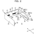
- FIG. 2 is a perspective view of a housing of the electronic device according to the first embodiment with part of the housing omitted.
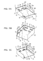
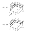
- FIGs. 3A to 3E are explanatory diagrams illustrating an example of an assembly process of the electronic device according to the first embodiment.
- FIGs. 4A to 4C are explanatory diagrams illustrating the example of the assembly process of the electronic device according to the first embodiment.
- FIG. 5 is an exploded perspective view of an electronic device according to a second embodiment with part of the electronic device omitted.
- FIG. 6 is a perspective view of a housing of the electronic device according to the second embodiment with part of the housing of the electronic device omitted.
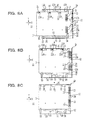
- FIGs. 7A to 7E are explanatory diagrams illustrating an example of an assembly process of the electronic device according to the second embodiment.
- FIGs. 8A to 8C are explanatory diagrams illustrating the example of the assembly process of the electronic device according to the second embodiment.
- FIGs. 9A and 9B are respectively an exploded perspective view and a perspective view of an electronic device in which a plurality of daughter boards are mounted with part of the electronic device omitted.
- FIG. 1 is an exploded perspective view of an electronic device according to a first embodiment with part of the electronic device omitted.
- FIG. 2 is a perspective view of a housing of the electronic device according to the first embodiment with part of the housing omitted.
- An electronic device 1 illustrated in FIG. 1 includes a housing 2 and a daughter board 3 that is mounted in the housing 2.
- the housing 2 has a front portion 2A, a rear surface portion 2B, a first side surface portion 2C, a second side surface portion 2D, a top surface portion (not illustrated), and a bottom surface portion (not illustrated).
- the front portion 2A is defined by an opening portion 11.
- the rear surface portion 2B opposes the front portion 2A.
- the first side surface portion 2C is adjacent to the rear surface portion 2B.
- the second side surface portion 2D is adjacent to the rear surface portion 2B and opposes the first side surface portion 2C.
- a first backplane 12 is disposed on the rear surface portion 2B,
- the first backplane 12 includes two first connectors 13 disposed thereon as an example.
- Each of the first connectors 13 is a straight connector having an engagement surface 13A on the front surface portion thereof.
- a second backplane 14 is disposed on the first side surface portion 2C.
- the second backplane 14 includes three second connectors 15 disposed thereon as an example.
- Each of the second connectors 15 is a right-angle connector having an engagement surface 15A on the side surface portion thereof.
- the daughter board 3 includes two straight third connectors 21 disposed on a leading end area 3A side thereof.
- the third connectors 21 are engaged with the first connectors 13 of the first backplane 12.
- the daughter board 3 also includes three right-angle fourth connectors 22 disposed on a first side surface portion 3B side thereof.
- the fourth connectors 22 are engaged with the second connectors 15 of the second backplane 14.
- the housing 2 has guide rails 16 disposed therein on the first side surface portion 2C and the second side surface portion 2D thereof.
- the guide rails 16 contact a lower surface of the daughter board 3 inserted through the opening portion 11, and hold the daughter board 3 such that the daughter board 3 is slidable relative to the guide rails 16.
- the guide rails 16 hold the daughter board 3 such that the daughter board 3 is perpendicular to the rear surface portion 2B, the first side surface portion 2C, and the second side surface portion 2D while the first connectors 13, the third connectors 21, the second connectors 15, and the fourth connectors 22 are horizontally disposed.
- a guide mechanism 17 is provided on the second side surface portion 2D inside the housing 2.
- the guide mechanism 17 guides the daughter board 3 inserted through the opening portion 11 into the housing 2.
- the guide mechanism 17 contacts a side surface portion 3C of the daughter board 3 and guides the daughter board 3 held on the guide rails 16 in a direction in which the daughter board 3 is inserted into the housing 2.
- this insertion direction is the X-direction
- a horizontal direction of the plane of the daughter board 3 that is directed toward the first side surface portion 2C and perpendicular to the X-direction is the Y-direction.
- the guide mechanism 17 has a guide groove member 30 that is provided on the second side surface portion 2D.
- the guide groove member 30 has a guide groove 31 formed therein.
- the second side surface portion 3C of the daughter board 3 inserted through the opening portion 11 contacts the guide groove 31 while sliding in the guide groove 31.
- the guide groove 31 guides the daughter board 3 from the start of insertion to the completion of mounting via following positions: a linear movement start position 30A, a parallel movement start position 30B, a parallel movement end position 30C, and a linear movement end position 30D.
- a linear movement of the daughter board 3 in the X-direction in the guide groove 31 starts at the linear movement start position 30A when the daughter board 3 is slid.
- the parallel movement start position 30B the linear movement of the daughter board 3 in the X-direction started from the linear movement start position 30A is stopped, and parallel movement of the daughter board 3 in the guide groove 31 in a diagonal direction toward the first side surface portion 2C side starts.
- the parallel movement end position 30C the parallel movement of the daughter board 3 in a diagonal direction toward the first side surface portion 2C side is complete, and the linear movement of the daughter board 3 in the X-direction in the guide groove 31 restarts.
- the linear movement end position 30D the linear movement of the daughter board 3 in the X-direction in the guide groove 31 is complete.
- the guide groove 31 includes a first guide groove 31A, a second guide groove 31B, and a third guide groove 31C.
- the second guide groove 31B is continuous with the first guide groove 31A
- the third guide groove 31C is continuous with the second guide groove 31B.
- the first guide groove 31A guides the daughter board 3 between the linear movement start position 30A and the parallel movement start position 30B.
- the first guide groove 31A guides the daughter board 3 so as to prevent the fourth connectors 22 from interfering with the second connectors 15 in the linear movement in the X-direction.
- the second guide groove 31B guides the daughter board 3 between the parallel movement start position 30B and the parallel movement end position 30C.
- the second guide groove 31B makes the daughter board 3 sliding toward the first backplane 12 undergo the parallel movement in a sliding manner from the second side surface portion 2D toward the first side surface portion 2C.
- the daughter board 3 is guided to a position in which engagement surfaces 22A of the fourth connectors 22 to be engaged with the second connectors 15 oppose the engagement surfaces 15A of the second connectors 15.
- the daughter board 3 is guided to a position in which engagement surfaces 21A of the third connectors 21 to be engaged with the first connectors 13 oppose the engagement surfaces 13A of the first connectors 13.
- the third guide groove 31C guides the daughter board 3 between the parallel movement end position 30C and the linear movement end position 30D.
- the third guide groove 31C makes the daughter board 3 restart the linear movement in the X-direction.
- the third connectors 21 are engaged with the first connectors 13, and the fourth connectors 22 are engaged with the second connectors 15.
- the daughter board 3 is guided by the first guide groove 31A, the second guide groove 31B, and the third guide groove 31C to be connected to the first side surface portion 2C and the first backplane 12 with a single operation.
- the distance between the parallel movement end position 30C to the linear movement end position 30D is equal to or greater than the moving distance of the third connectors 21 between a position at which engagement of the third connectors 21 with the first connectors 13 starts and a position at which the engagement of third connectors 21 with the first connectors 13 is complete.
- the side surface portion 3C of the daughter board 3 has a protruding portion 41 that protrudes at a position in a rearward direction of the daughter board 3, for example, at a position spaced away from a leading end portion 3D by a distance equal to the distance between the linear movement start position 30A and the parallel movement start position 308.
- the protruding portion 41 reaches the linear movement start position 30A in the first guide groove 31A.
- the protruding portion 41 assists the daughter board 3 in undergoing the parallel movement in a sliding manner toward the first side surface portion 2C side as the protruding portion 41 enters the first guide groove 31A.
- the protruding portion 41 protrudes from the surface of the side surface portion 3C by a dimension L1.
- L1 is equal to the distance of movement L2 in Y-direction, by which the daughter board 3 undergoes the parallel movement in the second guide groove 31B from the second side surface portion 2D side toward the first side surface portion 2C side (see FIG. 3A ).
- FIGs. 3A to 3E and FIGs. 4A to 4C are explanatory diagrams illustrating an example of an assembly process of the electronic device 1 according to the first embodiment.
- the daughter board 3 is inserted into the housing 2 through the opening portion 11.
- the daughter board 3 is guided into the housing 2 as illustrated in FIG. 3A while the side surface portion 3C of the daughter board 3 slides in the first guide groove 31A.
- the daughter board 3 is guided into the housing 2 in the X-direction through the first guide groove 31A.
- the daughter board 3 is held on the guide rails 16 formed on the first side surface portion 2C and the second side surface portion 2D.
- the daughter board 3 is held perpendicularly to the first backplane 12 and the second backplane 14 while the first connectors 13, the third connectors 21, the second connectors 15, and the fourth connectors 22 are horizontally disposed.
- the daughter board 3 undergoes the linear movement in the X-direction on the guide rails 16 until the leading end portion 3D of the side surface portion 3C thereof reaches the parallel movement start position 30B through the first guide groove 31A.
- the protruding portion 41 located in a rearward direction of the daughter board 3 enters the first guide groove 31A, As illustrated in FIG.
- the leading end portion 3D of the side surface portion 3C of the daughter board 3 enters the third guide groove 31C and reaches the linear movement end position 30D as the daughter board 3 undergoes the linear movement in the X-direction.
- the third connectors 21 are engaged with the first connectors 13, and the fourth connectors 22 are engaged with the second connectors 15.
- the daughter board 3 is mounted perpendicularly to the first backplane 12 and the second backplane 14.
- the daughter board 3 is guided through the guide groove 31 to a position at which the engagement surfaces 21A of the third connectors 21 and the engagement surfaces 13A of the first connectors 13 oppose each other, and the engagement surfaces 22A of the fourth connectors 22 and the engagement surfaces 15A of the second connectors 15 oppose each other.
- the daughter board 3 is mounted perpendicularly to the first backplane 12 and the second backplane 14 by engaging the third connectors 21 with the first connectors 13 and engaging the fourth connectors 22 with the second connectors 15.
- a work burden in mounting the daughter board 3 in a direction perpendicular to the first backplane 12 and the second backplane 14 may be reduced.
- the non-uniform density of wiring on the daughter board 3 is suppressed. This allows the number of daughter boards 3 to be mounted to be decreased.
- the daughter board 3 is caused to undergo the parallel movement in a diagonal direction toward the first side surface portion 2C side through the guide groove 31 of the guide groove member 30,
- a guide protruding portion may be formed instead of the guide groove 31, and the daughter board 3 may have a guide recess portion in the side surface portion 3C thereof.
- the guide protruding portion slides in the guide recess portion so as to cause the daughter board 3 to undergo the parallel movement in a diagonal direction toward the first side surface portion 2C side.
- the guide mechanism 17 may use a guide surface that allows the side surface portion 3C of the daughter board 3 to slide along the guide surface so as to cause the daughter board 3 to undergo the parallel movement in a diagonal direction toward the first side surface portion 2C side without use of the guide groove 31 or the guide protruding portion.
- the guide groove member 30 having the guide groove 31 is disposed on the second side surface portion 2D.
- the guide groove 31 may be directly formed in the second side surface portion 2D.
- the protruding portion 41 formed on the side surface portion 3C of the daughter board 3 enters the first guide groove 31A so as to assist the parallel movement of the daughter board 3 as the protruding portion 41 interferes with the guide groove 31.
- formation of the protruding portion 41 may be omitted.
- the guide groove member 30 exemplifies the guide mechanism 17.
- a lever member may be pivotally disposed on the second side surface portion 2D instead of the guide groove member 30 so as to cause the daughter board 3 to undergo the parallel movement toward the first side surface portion 2C side.
- An embodiment in this case will be described below as a second embodiment.
- FIG. 5 is an exploded perspective view of an electronic device 1A according to a second embodiment with part of the electronic device 1A omitted.
- FIG. 6 is a perspective view of a housing 2a of the electronic device 1A according to the second embodiment with part of the housing 2a omitted.
- Components similar to those of the electronic device 1 according to the first embodiment are denoted by the same reference signs in order to omit duplicate descriptions of structures and operations thereof.
- a main difference between the electronic device 1A illustrated in FIG. 5 and the electronic device 1 illustrated in FIG. 1 is that, in the electronic device 1A, the guide mechanism 17 provided on the second side surface portion 2D uses a lever member 50 instead of the guide groove member 30.
- the lever member 50 is pivotally disposed on one of the guide rails 16 formed on the second side surface portion 2D.
- the lever member 50 has a base member 51, a lever portion 52, a guide portion 53, and a fulcrum 54.
- the lever portion 52 is formed in a front end portion of the base member 51.
- the guide portion 53 is formed in a rear end portion of the base member 51.
- the lever portion 52 and the guide portion 53 are pivotable about the fulcrum 54.
- the guide portion 53 of the lever member 50 guides a daughter board 3a in the X-direction into the housing 2a while allowing the side surface portion 3C of the daughter board 3a inserted through the opening portion 11 to slide along the guide portion 53.
- the daughter board 3a is disposed perpendicularly to the first backplane 12 and the second backplane 14 while the first connectors 13, the third connectors 21, the second connectors 15, and the fourth connectors 22 are horizontally disposed.
- the lever portion 52 of the lever member 50 is pressed by the leading end portion 3D of the side surface portion 3C of the daughter board 3a in accordance with the linear movement in the X-direction of the daughter board 3a, which has been inserted from the opening portion 11.
- the lever portion 52 pivots about the fulcrum 54 toward the second side surface portion 2D side in accordance with a pressing operation performed by the leading end portion 3D.
- the guide portion 53 of the lever member 50 pivots about the fulcrum 54 toward the first side surface portion 2C side as the lever portion 52 pivots toward the second side surface portion 2D side.
- the guide portion 53 presses the side surface portion 3C of the daughter board 3a in a diagonal direction toward the first side surface portion 2C side as the guide portion 53 pivots toward the first side surface portion 2C side.
- the guide portion 53 causes the daughter board 3a to undergo a parallel movement to a position at which the engagement surfaces 21A of the third connectors 21 and the engagement surfaces 13A of the first connectors 13 oppose each other, and the engagement surfaces 22A of the fourth connectors 22 and the engagement surfaces 15A of the second connectors 15 oppose each other.
- the lever portion 52 of the lever member 50 causes the daughter board 3a to undergo a parallel movement in a diagonal direction toward the first side surface portion 2C side in accordance with the pressing operation performed by the leading end portion 3D of the daughter board 3a.
- the fever portion 52 is brought out of contact with the leading end portion 3D of the daughter board 3a at a timing at which the parallel movement of the daughter board 3a toward the first side surface portion 2C side is complete.
- the daughter board 3a undergoes a linear movement in the X-direction into the housing 2a from a position at which the engagement surfaces 21A of the third connectors 21 and the engagement surfaces 13A of the first connectors 13 oppose each other, and the engagement surfaces 22A of the fourth connectors 22 and the engagement surfaces 15A of the second connectors 15 oppose each other.
- the daughter board 3a is mounted perpendicularly to the first backplane 12 and the second backplane 14 by engaging the third connectors 21 with the first connectors 13 and engaging the fourth connectors 22 with the second connectors 15.
- FIGs. 7A to 7E and FIGs. 8A to 8C are explanatory diagrams illustrating an example of an assembly process of the electronic device 1A according to the second embodiment.
- the daughter board 3a is inserted into the housing 2a by the user.
- the daughter board 3a is inserted into the housing 2a in the X-direction as illustrated in FIG. 7A while the side surface portion 3C thereof slides from the opening portion 11 along the lever member 50 on the second side surface portion 2D side.
- the daughter board 3a is held on the guide rails 16 formed on the first side surface portion 2C and the second side surface portion 2D in the housing 2a.
- the daughter board 3a is held perpendicularly to the first backplane 12 and the second backplane 14 while the first connectors 13, the third connectors 21, the second connectors 15, and the fourth connectors 22 are horizontally disposed.
- the daughter board 3a When the daughter board 3a is inserted into the housing 2a in the X-direction, the daughter board 3a undergoes a linear movement in the X-direction on the guide rails 16 as illustrated in FIG. 7B .
- the leading end portion 3D of the side surface portion 3C of the daughter board 3a presses the lever portion 52 of the lever member 50 as the daughter board 3a undergoes the linear movement in the X-direction.
- the lever portion 52 of the lever member 50 pivots about the fulcrum 54 toward the second side surface portion 2D side in accordance with the pressing operation performed by the daughter board 3a.
- the guide portion 53 of the lever member 50 pivots toward the first side surface portion 2C side as the lever portion 52 undergoes the pivotal movement toward the second side surface portion 2D side,
- a rear end portion of the daughter board 3a starts the parallel movement in a diagonal direction toward the first side surface portion 2C in accordance with the pivotal movement of the guide portion 53 of the lever member 50 toward the first side surface portion 2C side.
- the lever portion 52 of the lever member 50 is brought out of contact with the leading end portion 3D of the daughter board 3a at a timing at which the parallel movement of the daughter board 3a toward the first side surface portion 2C side is complete as illustrated in FIGs. 7C and 7D .
- the lever portion 52 stops the pivotal movement toward the second side surface portion 2D side when the lever portion 52 is brought out of contact with the leading end portion 3D of the daughter board 3a.
- the guide portion 53 also stops the pivotal movement toward the first side surface portion 2C side.
- the daughter board 3a is guided to a position at which the engagement surfaces 21A of the third connectors 21 and the engagement surfaces 13A of the first connectors 13 oppose each other, and the engagement surfaces 22A of the fourth connectors 22 and the engagement surfaces 15A of the second connectors 15 oppose each other.
- the daughter board 3a undergoes the linear movement in the X-direction while the pivotal movement of the guide portion 53 toward the first side surface portion 2C side is stopped. As illustrated in FIGs. 7E and 8C , the third connectors 21 of the daughter board 3a are engaged with the first connectors 13, and the fourth connectors 22 of the daughter board 3a are engaged with the second connectors 15. As a result, the daughter board 3a is mounted perpendicularly to the first backplane 12 and the second backplane 14.
- the lever portion 52 of the lever member 50 pivots toward the second side surface portion 2D side in accordance with the linear movement of the leading end portion 3D of the daughter board 3a in the X-direction caused with a single insertion operation.
- the guide portion 53 of the lever member 50 pivots toward the first side surface portion 2C side as the lever portion 52 undergoes a pivotal movement.
- the guide portion 53 causes the daughter board 3a to undergo the parallel movement in a diagonal direction toward the first side surface portion 2C side as the guide portion 53 undergoes the pivotal movement toward the first side surface portion 2C side.
- the daughter board 3a is guided to the position at which the engagement surfaces 21A of the third connectors 21 and the engagement surfaces 13A of the first connectors 13 oppose each other, and the engagement surfaces 22A of the fourth connectors 22 and the engagement surfaces 15A of the second connectors 15 oppose each other.
- the daughter board 3a is mounted perpendicularly to the first backplane 12 and the second backplane 14 by engaging the first connectors 13 with the third connectors 21 and engaging the second connectors 15 with the fourth connectors 22.
- a work burden in mounting the daughter board 3a perpendicularly to the first backplane 12 and the second backplane 14 may be reduced.
- first backplane 12 and the second backplane 14 are respectively disposed on the rear surface portion 2B and the first side surface portion 2C in the housing 2 or 2a.
- two backplanes may be disposed on the rear surface portion 2B and the second side surface portion 2D, on the top surface portion and the first side surface portion 2C, on the top surface portion and the second side surface portion 2D, on the bottom surface portion and the first side surface portion 2C, on the bottom surface portion and the second side surface portion 2D, or the like.
- one daughter board 3 or 3a is perpendicularly mounted to the first backplane 12 and the second backplane 14. Similar advantages are obtainable when a plurality of daughter boards 3 or 3a are mounted to the first backplane 12 and second backplane 14.
- FIGs. 9A and 9B are respectively an exploded perspective view and a perspective view of an electronic device 1B in which a plurality of daughter boards 3 are mounted with part of the electronic device 1B omitted.
- a plurality of daughter board 3a may similarly be mounted in a housing of an electronic device.
- components similar to those of the electronic device 1 illustrated in FIG. 1 are denoted by the same reference signs in order to omit duplicate descriptions of structures and operations thereof.
- FIGs. 9A and 9B use the guide mechanism 17 (not illustrated) to sequentially mount the daughter boards 3 perpendicularly to the first backplane 12 and the second backplane 14.
- the electronic device 1B allows the plurality of daughter boards 3 to be easily mounted to the first backplane 12 and the second backplane 14.
- a jumper 61 may be used to connect the daughter boards 3 to each other.
- the daughter board 3 or 3a when the daughter board 3 or 3a is inserted into the housing 2 or 2a, the daughter board 3 or 3a is caused to undergo the linear movement in the X-direction while occurrence of a situation in which the fourth connectors 22 interfere with the second connectors 15 is avoided, and the daughter board 3 or 3a is caused to undergo the parallel movement in a diagonal direction toward the first side surface portion 2C side.
- the daughter board 3 or 3a having undergone the parallel movement is again caused to undergo the linear movement in the X-direction.
- engagement of the third connectors 21 of the daughter board 3 or 3a with the first connectors 13 and engagement of the fourth connectors 22 of the daughter board 3 or 3a with the second connectors 15 simultaneously occur.
- the connectors are engaged with each other without a work space in which the daughter board 3 or 3a is moved in the perpendicular direction.
- the work space is not required, thereby allowing the size of the electronic device to be decreased by decreasing a distance between positions at which the daughter boards 3 or 3a are mounted.
- the daughter board 3 or 3a is perpendicularly mounted to the first backplane 12 and the second backplane 14.
- occurrence of a situation in which connectors to be engaged with those of the daughter board 3 or 3a are concentrated in the rear surface portion 2B of the first backplane 12 is avoidable.
- This may decrease the number of connectors mounted on the first backplane 12 on the rear surface portion 2B side opposing the opening portion 11, and accordingly, a space in which a vent hole is disposed may be allocated in the rear surface portion 2B.
- cooling air flows from the opening portion 11 to the vent hole of the rear surface portion 2B in a certain direction, that is, in the X-direction, and accordingly, cooling efficiency may be improved.
Landscapes
- Engineering & Computer Science (AREA)
- Microelectronics & Electronic Packaging (AREA)
- Mounting Of Printed Circuit Boards And The Like (AREA)
- Coupling Device And Connection With Printed Circuit (AREA)
Applications Claiming Priority (1)
| Application Number | Priority Date | Filing Date | Title |
|---|---|---|---|
| JP2011057108A JP5655648B2 (ja) | 2011-03-15 | 2011-03-15 | 電子装置及び回路基板の接続構造 |
Publications (2)
| Publication Number | Publication Date |
|---|---|
| EP2500988A2 true EP2500988A2 (fr) | 2012-09-19 |
| EP2500988A3 EP2500988A3 (fr) | 2015-03-04 |
Family
ID=45936755
Family Applications (1)
| Application Number | Title | Priority Date | Filing Date |
|---|---|---|---|
| EP20120159435 Withdrawn EP2500988A3 (fr) | 2011-03-15 | 2012-03-14 | Dispositif électronique et structure de connexion pour carte de circuit |
Country Status (3)
| Country | Link |
|---|---|
| US (1) | US9019711B2 (fr) |
| EP (1) | EP2500988A3 (fr) |
| JP (1) | JP5655648B2 (fr) |
Cited By (1)
| Publication number | Priority date | Publication date | Assignee | Title |
|---|---|---|---|---|
| WO2017129745A1 (fr) * | 2016-01-29 | 2017-08-03 | Avl List Gmbh | Dispositif d'entraînement et de commande pour débitmètre |
Families Citing this family (30)
| Publication number | Priority date | Publication date | Assignee | Title |
|---|---|---|---|---|
| US9136621B1 (en) * | 2012-08-14 | 2015-09-15 | Ciena Corporation | Guides and tab arrangement to retain a card having an edge connector and method of use |
| JP6229361B2 (ja) * | 2013-08-01 | 2017-11-15 | 富士通株式会社 | 電子機器及び基板ユニット |
| CN105578828B (zh) * | 2016-01-11 | 2018-07-17 | 俞岳田 | 一种可自动插拔电路板的通讯设备 |
| CN105592658B (zh) * | 2016-01-11 | 2018-06-19 | 安溪县百家宜家居用品有限公司 | 一种具有电路板自动插拔功能且可快速散热的通讯设备 |
| CN105658013B (zh) * | 2016-01-11 | 2018-07-17 | 岑浩明 | 一种可减震且能自动插拔电路板的通讯设备 |
| CN105430995B (zh) * | 2016-01-11 | 2018-07-17 | 俞岳田 | 一种可防震且可自动插拔电路板的通讯设备 |
| CN105578826B (zh) * | 2016-01-11 | 2018-07-17 | 岑浩明 | 一种带有led指示灯可自动插拔电路板的通讯设备 |
| CN105430994B (zh) * | 2016-01-11 | 2018-04-17 | 戎佰腾 | 一种安装有电子控制器且可自动插拔电路板的通讯设备 |
| CN105451501B (zh) * | 2016-01-11 | 2018-04-17 | 戎佰腾 | 一种带有滚轮且可自动插拔电路板的通讯设备 |
| CN105611778B (zh) * | 2016-01-11 | 2018-05-25 | 泉州市港生利来进出口贸易有限公司 | 一种具有电路板自动插拔功能且可提示的通讯设备 |
| CN105611777B (zh) * | 2016-01-11 | 2018-06-22 | 温岭市海玛进出口有限公司 | 一种具有电路板自动插拔功能且带有滚轮的通讯设备 |
| CN105578827B (zh) * | 2016-01-11 | 2018-07-17 | 俞岳田 | 一种可散热且可自动插拔电路板的通讯设备 |
| US10832101B2 (en) * | 2016-07-29 | 2020-11-10 | Hewlett-Packard Development Company, L.P. | Electronic card holders |
| JP6631581B2 (ja) * | 2017-04-17 | 2020-01-15 | 株式会社デンソー | 電子装置 |
| US10694635B1 (en) * | 2018-08-14 | 2020-06-23 | Amazon Technologies, Inc. | Mesh network topology based on midplane board |
| JP7201424B2 (ja) * | 2018-12-25 | 2023-01-10 | ファナック株式会社 | 電子装置 |
| US11378608B2 (en) | 2019-07-19 | 2022-07-05 | Dell Products L.P. | System and method for device state determination |
| US10980159B2 (en) | 2019-07-19 | 2021-04-13 | Dell Products L.P. | System and method for managing multiple connections |
| US11132038B2 (en) | 2019-07-19 | 2021-09-28 | Dell Products L.P. | System and method for thermal management of shadowed devices |
| US11122718B2 (en) | 2019-07-19 | 2021-09-14 | Dell Products L.P. | System and method for device level electromagnetic interference management |
| US11143682B2 (en) | 2019-07-19 | 2021-10-12 | Dell Products L.P. | System and method for communicating externally from an electromagnetic interference suppressed volume |
| US11399450B2 (en) | 2019-07-19 | 2022-07-26 | Dell Products L.P. | System and method for managing electromagnetic interference |
| US11234347B2 (en) * | 2019-07-19 | 2022-01-25 | Dell Products L.P. | System and method for physical management of devices |
| US11644425B2 (en) | 2019-07-19 | 2023-05-09 | Dell Products L.P. | System and method for optical state determination |
| US11129307B2 (en) | 2019-07-19 | 2021-09-21 | Dell Products L.P. | System and method for managing thermal states of devices |
| US10917996B1 (en) | 2019-07-19 | 2021-02-09 | Dell Products L.P. | System and method for device level thermal management and electromagnetic interference management |
| US11147194B2 (en) | 2019-08-21 | 2021-10-12 | Dell Products L.P. | System and method for managing electromagnetic interference |
| US11234350B2 (en) | 2019-08-21 | 2022-01-25 | Dell Products L.P. | System and method for isolated device access |
| TWI719603B (zh) * | 2019-08-23 | 2021-02-21 | 緯創資通股份有限公司 | 連接模組和電子裝置 |
| CN216412150U (zh) * | 2021-08-11 | 2022-04-29 | 富联精密电子(天津)有限公司 | OCP转接装置、OCP板卡和PCIe板卡兼容托架组件及服务器 |
Citations (3)
| Publication number | Priority date | Publication date | Assignee | Title |
|---|---|---|---|---|
| JPS50119282A (fr) | 1974-03-08 | 1975-09-18 | ||
| JP2002223085A (ja) | 2001-01-25 | 2002-08-09 | Hitachi Ltd | プリント基板とバックボードとの接続構造、及びプリント基板とバックボードに搭載のボードtoボードコネクタ |
| JP2006164627A (ja) | 2004-12-03 | 2006-06-22 | Fujitsu Ltd | コネクタ、プリント配線基板実装装置およびプリント配線基板実装方法 |
Family Cites Families (21)
| Publication number | Priority date | Publication date | Assignee | Title |
|---|---|---|---|---|
| JPS50105553U (fr) * | 1974-02-06 | 1975-08-30 | ||
| US6457647B1 (en) * | 1993-11-16 | 2002-10-01 | Canon Kabushiki Kaisha | Memory card adaptor to facilitate upgrades and the like |
| US5559317A (en) * | 1995-03-27 | 1996-09-24 | International Verifact Inc. | Card reader with carriage powered by movement of inserted card |
| US5644470A (en) | 1995-11-02 | 1997-07-01 | International Business Machines Corporation | Autodocking hardware for installing and/or removing adapter cards without opening the computer system cover |
| JPH1117367A (ja) * | 1997-06-26 | 1999-01-22 | Fujitsu I Network Syst Ltd | パッケージ実装方式 |
| JP3288277B2 (ja) * | 1997-09-16 | 2002-06-04 | アルプス電気株式会社 | Icカード用コネクタ |
| GB9807989D0 (en) | 1998-04-16 | 1998-06-17 | Babin Andre | Extension card insertion and removal system |
| JP3806271B2 (ja) * | 1999-07-09 | 2006-08-09 | 日本電産サンキョー株式会社 | 磁気カード取引装置 |
| JP3635625B2 (ja) * | 1999-11-05 | 2005-04-06 | 山一電機株式会社 | カードコネクタのスイッチ構造 |
| JP3338415B2 (ja) * | 1999-12-28 | 2002-10-28 | 山一電機株式会社 | カードコネクタ |
| EP1295364A2 (fr) * | 2000-06-29 | 2003-03-26 | Molex Incorporated | Connecteur de cartes a circuit integre |
| US20030033463A1 (en) * | 2001-08-10 | 2003-02-13 | Garnett Paul J. | Computer system storage |
| DE10203066A1 (de) * | 2002-01-28 | 2003-08-07 | Marconi Comm Gmbh | Leiterplatten-Bestückungssystem sowie Verfahren zum Positionieren von Leiterplatten |
| JP2004031806A (ja) * | 2002-06-27 | 2004-01-29 | Fujitsu Ltd | 電子回路ユニットの挿抜機構 |
| US6940727B2 (en) * | 2003-10-08 | 2005-09-06 | Hewlett-Packard Development Company, L.P. | Card guide that comprises card guide portions that serve to guide a circuit board into a chassis |
| JP2006024761A (ja) * | 2004-07-08 | 2006-01-26 | Matsushita Electric Ind Co Ltd | 無線基地局のユニットスライド構造 |
| JP4711194B2 (ja) | 2006-03-14 | 2011-06-29 | 日本電気株式会社 | 回路基板装置及びコネクタの挿抜方法 |
| KR101348247B1 (ko) * | 2007-06-07 | 2014-01-09 | 삼성디스플레이 주식회사 | 액정 표시 장치 |
| JP2010067192A (ja) * | 2008-09-12 | 2010-03-25 | Fujitsu Ltd | 電子機器 |
| JP5245923B2 (ja) | 2009-03-05 | 2013-07-24 | 富士通株式会社 | 電子機器システム及び基板の挿抜治具 |
| US8199511B2 (en) * | 2009-04-01 | 2012-06-12 | Fusion-Io, Inc. | Hot swappable computer card carrier |
-
2011
- 2011-03-15 JP JP2011057108A patent/JP5655648B2/ja not_active Expired - Fee Related
-
2012
- 2012-03-13 US US13/419,064 patent/US9019711B2/en not_active Expired - Fee Related
- 2012-03-14 EP EP20120159435 patent/EP2500988A3/fr not_active Withdrawn
Patent Citations (3)
| Publication number | Priority date | Publication date | Assignee | Title |
|---|---|---|---|---|
| JPS50119282A (fr) | 1974-03-08 | 1975-09-18 | ||
| JP2002223085A (ja) | 2001-01-25 | 2002-08-09 | Hitachi Ltd | プリント基板とバックボードとの接続構造、及びプリント基板とバックボードに搭載のボードtoボードコネクタ |
| JP2006164627A (ja) | 2004-12-03 | 2006-06-22 | Fujitsu Ltd | コネクタ、プリント配線基板実装装置およびプリント配線基板実装方法 |
Cited By (1)
| Publication number | Priority date | Publication date | Assignee | Title |
|---|---|---|---|---|
| WO2017129745A1 (fr) * | 2016-01-29 | 2017-08-03 | Avl List Gmbh | Dispositif d'entraînement et de commande pour débitmètre |
Also Published As
| Publication number | Publication date |
|---|---|
| JP5655648B2 (ja) | 2015-01-21 |
| US9019711B2 (en) | 2015-04-28 |
| EP2500988A3 (fr) | 2015-03-04 |
| JP2012195387A (ja) | 2012-10-11 |
| US20120236521A1 (en) | 2012-09-20 |
Similar Documents
| Publication | Publication Date | Title |
|---|---|---|
| US9019711B2 (en) | Electronic device and connection structure for circuit board | |
| JP5660756B2 (ja) | 基板対基板コネクタ | |
| US7510416B2 (en) | PIU plug-in/plug-off mechanism for electronic apparatus | |
| JP5197294B2 (ja) | 基板対基板コネクタ | |
| US8292648B2 (en) | Flexible cable connecting structure and flexible cable connector | |
| US8328571B2 (en) | Connector assemblies having moveable mating arrays and power connectors | |
| US9867307B2 (en) | Information processing apparatus | |
| US9356373B2 (en) | Connector for electrical connection of a plate-shaped object | |
| US7361043B2 (en) | Apparatus including card element, device inserted into apparatus and a method for connecting or disconnecting the card element | |
| TW200843215A (en) | Connector capable of absorbing an error in mounting position | |
| JP2010123690A (ja) | プリント基板およびプリント基板搭載構造 | |
| US8282290B2 (en) | Connectors and assemblies having a plurality of moveable mating arrays | |
| JP7002432B2 (ja) | コネクタ及びコネクタの製造方法 | |
| US9685749B1 (en) | Cable limiting device and server thereof | |
| KR102395645B1 (ko) | 기판 커넥터용 컨택트 및 기판 커넥터 | |
| KR20130032518A (ko) | Fpc 커넥터 | |
| TW201832420A (zh) | 機構件、使用該機構件之方法、具有該機構件之系統及組件 | |
| JP5842571B2 (ja) | 電気コネクタ | |
| JP2004213934A (ja) | 接続部品、及びコネクタ装置 | |
| JP4371836B2 (ja) | 電子ユニットを接続するための装置 | |
| WO2013159367A1 (fr) | Module d'affichage à cristaux liquides, dispositif d'affichage à cristaux liquides, et panneau arrière | |
| JP4559296B2 (ja) | 平形の接続部材の接続構造およびこれを用いた基板対基板の接続構造 | |
| JP7053975B1 (ja) | スライドレール及び電子機器 | |
| JP2007242515A (ja) | フラットケーブル用電気コネクタ | |
| JP2019021530A (ja) | コネクタ及びこれを備えた電子機器 |
Legal Events
| Date | Code | Title | Description |
|---|---|---|---|
| PUAI | Public reference made under article 153(3) epc to a published international application that has entered the european phase |
Free format text: ORIGINAL CODE: 0009012 |
|
| AK | Designated contracting states |
Kind code of ref document: A2 Designated state(s): AL AT BE BG CH CY CZ DE DK EE ES FI FR GB GR HR HU IE IS IT LI LT LU LV MC MK MT NL NO PL PT RO RS SE SI SK SM TR |
|
| AX | Request for extension of the european patent |
Extension state: BA ME |
|
| PUAL | Search report despatched |
Free format text: ORIGINAL CODE: 0009013 |
|
| AK | Designated contracting states |
Kind code of ref document: A3 Designated state(s): AL AT BE BG CH CY CZ DE DK EE ES FI FR GB GR HR HU IE IS IT LI LT LU LV MC MK MT NL NO PL PT RO RS SE SI SK SM TR |
|
| AX | Request for extension of the european patent |
Extension state: BA ME |
|
| RIC1 | Information provided on ipc code assigned before grant |
Ipc: H05K 7/14 20060101ALI20150126BHEP Ipc: H01R 13/62 20060101AFI20150126BHEP Ipc: H01R 12/71 20110101ALI20150126BHEP |
|
| 17P | Request for examination filed |
Effective date: 20150806 |
|
| RBV | Designated contracting states (corrected) |
Designated state(s): AL AT BE BG CH CY CZ DE DK EE ES FI FR GB GR HR HU IE IS IT LI LT LU LV MC MK MT NL NO PL PT RO RS SE SI SK SM TR |
|
| STAA | Information on the status of an ep patent application or granted ep patent |
Free format text: STATUS: THE APPLICATION HAS BEEN WITHDRAWN |
|
| 18W | Application withdrawn |
Effective date: 20171129 |