EP2474505B1 - Procédé de formation d'une couche mince diélectrique et condensateur en couches minces comprenant ladite couche mince diélectrique - Google Patents
Procédé de formation d'une couche mince diélectrique et condensateur en couches minces comprenant ladite couche mince diélectrique Download PDFInfo
- Publication number
- EP2474505B1 EP2474505B1 EP10813781.1A EP10813781A EP2474505B1 EP 2474505 B1 EP2474505 B1 EP 2474505B1 EP 10813781 A EP10813781 A EP 10813781A EP 2474505 B1 EP2474505 B1 EP 2474505B1
- Authority
- EP
- European Patent Office
- Prior art keywords
- thin film
- baking
- film capacitor
- dielectric thin
- thickness
- Prior art date
- Legal status (The legal status is an assumption and is not a legal conclusion. Google has not performed a legal analysis and makes no representation as to the accuracy of the status listed.)
- Active
Links
- 239000010409 thin film Substances 0.000 title claims description 304
- 239000003990 capacitor Substances 0.000 title claims description 154
- 238000000034 method Methods 0.000 title claims description 55
- 239000012298 atmosphere Substances 0.000 claims description 40
- 239000000203 mixture Substances 0.000 claims description 39
- 239000010408 film Substances 0.000 claims description 36
- 238000000576 coating method Methods 0.000 claims description 35
- 239000011248 coating agent Substances 0.000 claims description 34
- 239000010936 titanium Substances 0.000 claims description 31
- 229910052719 titanium Inorganic materials 0.000 claims description 27
- 239000013078 crystal Substances 0.000 claims description 26
- 229910052788 barium Inorganic materials 0.000 claims description 24
- 229910052712 strontium Inorganic materials 0.000 claims description 24
- 238000010438 heat treatment Methods 0.000 claims description 21
- 239000000758 substrate Substances 0.000 claims description 15
- 230000015572 biosynthetic process Effects 0.000 claims description 13
- 150000001553 barium compounds Chemical class 0.000 claims description 9
- 239000012212 insulator Substances 0.000 claims description 9
- 150000003438 strontium compounds Chemical class 0.000 claims description 9
- 229910008593 TiyO3 Inorganic materials 0.000 claims description 7
- 238000001035 drying Methods 0.000 claims description 6
- 229910052751 metal Inorganic materials 0.000 claims description 6
- 239000002184 metal Substances 0.000 claims description 6
- -1 titanium alkoxide Chemical class 0.000 claims description 5
- 150000001732 carboxylic acid derivatives Chemical class 0.000 claims description 4
- 150000003839 salts Chemical class 0.000 claims description 4
- 125000001495 ethyl group Chemical group [H]C([H])([H])C([H])([H])* 0.000 claims description 3
- 125000004435 hydrogen atom Chemical group [H]* 0.000 claims description 3
- 125000002496 methyl group Chemical group [H]C([H])([H])* 0.000 claims description 3
- 239000003960 organic solvent Substances 0.000 claims description 3
- 230000000052 comparative effect Effects 0.000 description 82
- IJGRMHOSHXDMSA-UHFFFAOYSA-N Atomic nitrogen Chemical compound N#N IJGRMHOSHXDMSA-UHFFFAOYSA-N 0.000 description 29
- 229910001873 dinitrogen Inorganic materials 0.000 description 29
- BASFCYQUMIYNBI-UHFFFAOYSA-N platinum Chemical compound [Pt] BASFCYQUMIYNBI-UHFFFAOYSA-N 0.000 description 16
- VYPSYNLAJGMNEJ-UHFFFAOYSA-N Silicium dioxide Chemical compound O=[Si]=O VYPSYNLAJGMNEJ-UHFFFAOYSA-N 0.000 description 12
- 229910052681 coesite Inorganic materials 0.000 description 6
- 229910052906 cristobalite Inorganic materials 0.000 description 6
- 239000000377 silicon dioxide Substances 0.000 description 6
- 229910052682 stishovite Inorganic materials 0.000 description 6
- VXUYXOFXAQZZMF-UHFFFAOYSA-N titanium(IV) isopropoxide Chemical compound CC(C)O[Ti](OC(C)C)(OC(C)C)OC(C)C VXUYXOFXAQZZMF-UHFFFAOYSA-N 0.000 description 6
- 229910052905 tridymite Inorganic materials 0.000 description 6
- 238000011156 evaluation Methods 0.000 description 5
- 229910052697 platinum Inorganic materials 0.000 description 5
- 238000002360 preparation method Methods 0.000 description 4
- 238000004528 spin coating Methods 0.000 description 4
- 238000004544 sputter deposition Methods 0.000 description 4
- 238000000427 thin-film deposition Methods 0.000 description 4
- 238000001000 micrograph Methods 0.000 description 3
- 239000002994 raw material Substances 0.000 description 3
- 238000001771 vacuum deposition Methods 0.000 description 3
- 229910010252 TiO3 Inorganic materials 0.000 description 2
- 229910052454 barium strontium titanate Inorganic materials 0.000 description 2
- 229910002113 barium titanate Inorganic materials 0.000 description 2
- FWPJKASAXSYLKP-UHFFFAOYSA-L barium(2+);2-ethylbutanoate Chemical compound [Ba+2].CCC(CC)C([O-])=O.CCC(CC)C([O-])=O FWPJKASAXSYLKP-UHFFFAOYSA-L 0.000 description 2
- VJFFDDQGMMQGTQ-UHFFFAOYSA-L barium(2+);2-ethylhexanoate Chemical compound [Ba+2].CCCCC(CC)C([O-])=O.CCCCC(CC)C([O-])=O VJFFDDQGMMQGTQ-UHFFFAOYSA-L 0.000 description 2
- YHWCPXVTRSHPNY-UHFFFAOYSA-N butan-1-olate;titanium(4+) Chemical compound [Ti+4].CCCC[O-].CCCC[O-].CCCC[O-].CCCC[O-] YHWCPXVTRSHPNY-UHFFFAOYSA-N 0.000 description 2
- 150000007942 carboxylates Chemical class 0.000 description 2
- 230000007423 decrease Effects 0.000 description 2
- 230000007850 degeneration Effects 0.000 description 2
- MLFHJEHSLIIPHL-UHFFFAOYSA-N isoamyl acetate Chemical compound CC(C)CCOC(C)=O MLFHJEHSLIIPHL-UHFFFAOYSA-N 0.000 description 2
- 238000010030 laminating Methods 0.000 description 2
- 239000000463 material Substances 0.000 description 2
- 230000003647 oxidation Effects 0.000 description 2
- 238000007254 oxidation reaction Methods 0.000 description 2
- 239000012071 phase Substances 0.000 description 2
- 239000010970 precious metal Substances 0.000 description 2
- 238000007650 screen-printing Methods 0.000 description 2
- 238000003980 solgel method Methods 0.000 description 2
- XKFQWWYUSWDWTF-UHFFFAOYSA-L strontium;2-ethylbutanoate Chemical compound [Sr+2].CCC(CC)C([O-])=O.CCC(CC)C([O-])=O XKFQWWYUSWDWTF-UHFFFAOYSA-L 0.000 description 2
- DLWBHRIWCMOQKI-UHFFFAOYSA-L strontium;2-ethylhexanoate Chemical compound [Sr+2].CCCCC(CC)C([O-])=O.CCCCC(CC)C([O-])=O DLWBHRIWCMOQKI-UHFFFAOYSA-L 0.000 description 2
- 238000001947 vapour-phase growth Methods 0.000 description 2
- JRPBQTZRNDNNOP-UHFFFAOYSA-N barium titanate Chemical compound [Ba+2].[Ba+2].[O-][Ti]([O-])([O-])[O-] JRPBQTZRNDNNOP-UHFFFAOYSA-N 0.000 description 1
- IUQPAAJWHZCRBB-UHFFFAOYSA-N barium(2+) propan-2-olate Chemical compound CC([O-])C.CC([O-])C.CC([O-])C.CC([O-])C.[Ba+2].[Ba+2] IUQPAAJWHZCRBB-UHFFFAOYSA-N 0.000 description 1
- AESMDVCWMVZFRQ-UHFFFAOYSA-L barium(2+);butanoate Chemical compound [Ba+2].CCCC([O-])=O.CCCC([O-])=O AESMDVCWMVZFRQ-UHFFFAOYSA-L 0.000 description 1
- 239000003795 chemical substances by application Substances 0.000 description 1
- 238000005229 chemical vapour deposition Methods 0.000 description 1
- 238000010586 diagram Methods 0.000 description 1
- 238000003618 dip coating Methods 0.000 description 1
- IEEFJSJUHWAVJP-UHFFFAOYSA-N distrontium propan-2-olate Chemical compound [Sr++].[Sr++].CC(C)[O-].CC(C)[O-].CC(C)[O-].CC(C)[O-] IEEFJSJUHWAVJP-UHFFFAOYSA-N 0.000 description 1
- 230000000694 effects Effects 0.000 description 1
- 238000005516 engineering process Methods 0.000 description 1
- 230000002708 enhancing effect Effects 0.000 description 1
- 239000007789 gas Substances 0.000 description 1
- 229940117955 isoamyl acetate Drugs 0.000 description 1
- 238000000608 laser ablation Methods 0.000 description 1
- 238000001182 laser chemical vapour deposition Methods 0.000 description 1
- 238000004519 manufacturing process Methods 0.000 description 1
- 239000012299 nitrogen atmosphere Substances 0.000 description 1
- 230000001590 oxidative effect Effects 0.000 description 1
- 230000000704 physical effect Effects 0.000 description 1
- 238000005240 physical vapour deposition Methods 0.000 description 1
- 238000005507 spraying Methods 0.000 description 1
- VEALVRVVWBQVSL-UHFFFAOYSA-N strontium titanate Chemical compound [Sr+2].[O-][Ti]([O-])=O VEALVRVVWBQVSL-UHFFFAOYSA-N 0.000 description 1
- ITUCOQTVTSFGRJ-UHFFFAOYSA-L strontium;butanoate Chemical compound [Sr+2].CCCC([O-])=O.CCCC([O-])=O ITUCOQTVTSFGRJ-UHFFFAOYSA-L 0.000 description 1
- 239000000126 substance Substances 0.000 description 1
- 238000009279 wet oxidation reaction Methods 0.000 description 1
Images

Classifications
-
- C—CHEMISTRY; METALLURGY
- C04—CEMENTS; CONCRETE; ARTIFICIAL STONE; CERAMICS; REFRACTORIES
- C04B—LIME, MAGNESIA; SLAG; CEMENTS; COMPOSITIONS THEREOF, e.g. MORTARS, CONCRETE OR LIKE BUILDING MATERIALS; ARTIFICIAL STONE; CERAMICS; REFRACTORIES; TREATMENT OF NATURAL STONE
- C04B35/00—Shaped ceramic products characterised by their composition; Ceramics compositions; Processing powders of inorganic compounds preparatory to the manufacturing of ceramic products
- C04B35/622—Forming processes; Processing powders of inorganic compounds preparatory to the manufacturing of ceramic products
- C04B35/624—Sol-gel processing
-
- H—ELECTRICITY
- H01—ELECTRIC ELEMENTS
- H01B—CABLES; CONDUCTORS; INSULATORS; SELECTION OF MATERIALS FOR THEIR CONDUCTIVE, INSULATING OR DIELECTRIC PROPERTIES
- H01B5/00—Non-insulated conductors or conductive bodies characterised by their form
-
- C—CHEMISTRY; METALLURGY
- C01—INORGANIC CHEMISTRY
- C01G—COMPOUNDS CONTAINING METALS NOT COVERED BY SUBCLASSES C01D OR C01F
- C01G23/00—Compounds of titanium
- C01G23/003—Titanates
- C01G23/006—Alkaline earth titanates
-
- C—CHEMISTRY; METALLURGY
- C04—CEMENTS; CONCRETE; ARTIFICIAL STONE; CERAMICS; REFRACTORIES
- C04B—LIME, MAGNESIA; SLAG; CEMENTS; COMPOSITIONS THEREOF, e.g. MORTARS, CONCRETE OR LIKE BUILDING MATERIALS; ARTIFICIAL STONE; CERAMICS; REFRACTORIES; TREATMENT OF NATURAL STONE
- C04B35/00—Shaped ceramic products characterised by their composition; Ceramics compositions; Processing powders of inorganic compounds preparatory to the manufacturing of ceramic products
- C04B35/01—Shaped ceramic products characterised by their composition; Ceramics compositions; Processing powders of inorganic compounds preparatory to the manufacturing of ceramic products based on oxide ceramics
- C04B35/46—Shaped ceramic products characterised by their composition; Ceramics compositions; Processing powders of inorganic compounds preparatory to the manufacturing of ceramic products based on oxide ceramics based on titanium oxides or titanates
- C04B35/462—Shaped ceramic products characterised by their composition; Ceramics compositions; Processing powders of inorganic compounds preparatory to the manufacturing of ceramic products based on oxide ceramics based on titanium oxides or titanates based on titanates
- C04B35/465—Shaped ceramic products characterised by their composition; Ceramics compositions; Processing powders of inorganic compounds preparatory to the manufacturing of ceramic products based on oxide ceramics based on titanium oxides or titanates based on titanates based on alkaline earth metal titanates
- C04B35/468—Shaped ceramic products characterised by their composition; Ceramics compositions; Processing powders of inorganic compounds preparatory to the manufacturing of ceramic products based on oxide ceramics based on titanium oxides or titanates based on titanates based on alkaline earth metal titanates based on barium titanates
- C04B35/4686—Shaped ceramic products characterised by their composition; Ceramics compositions; Processing powders of inorganic compounds preparatory to the manufacturing of ceramic products based on oxide ceramics based on titanium oxides or titanates based on titanates based on alkaline earth metal titanates based on barium titanates based on phases other than BaTiO3 perovskite phase
-
- C—CHEMISTRY; METALLURGY
- C04—CEMENTS; CONCRETE; ARTIFICIAL STONE; CERAMICS; REFRACTORIES
- C04B—LIME, MAGNESIA; SLAG; CEMENTS; COMPOSITIONS THEREOF, e.g. MORTARS, CONCRETE OR LIKE BUILDING MATERIALS; ARTIFICIAL STONE; CERAMICS; REFRACTORIES; TREATMENT OF NATURAL STONE
- C04B35/00—Shaped ceramic products characterised by their composition; Ceramics compositions; Processing powders of inorganic compounds preparatory to the manufacturing of ceramic products
- C04B35/01—Shaped ceramic products characterised by their composition; Ceramics compositions; Processing powders of inorganic compounds preparatory to the manufacturing of ceramic products based on oxide ceramics
- C04B35/46—Shaped ceramic products characterised by their composition; Ceramics compositions; Processing powders of inorganic compounds preparatory to the manufacturing of ceramic products based on oxide ceramics based on titanium oxides or titanates
- C04B35/462—Shaped ceramic products characterised by their composition; Ceramics compositions; Processing powders of inorganic compounds preparatory to the manufacturing of ceramic products based on oxide ceramics based on titanium oxides or titanates based on titanates
- C04B35/465—Shaped ceramic products characterised by their composition; Ceramics compositions; Processing powders of inorganic compounds preparatory to the manufacturing of ceramic products based on oxide ceramics based on titanium oxides or titanates based on titanates based on alkaline earth metal titanates
- C04B35/47—Shaped ceramic products characterised by their composition; Ceramics compositions; Processing powders of inorganic compounds preparatory to the manufacturing of ceramic products based on oxide ceramics based on titanium oxides or titanates based on titanates based on alkaline earth metal titanates based on strontium titanates
-
- H—ELECTRICITY
- H01—ELECTRIC ELEMENTS
- H01B—CABLES; CONDUCTORS; INSULATORS; SELECTION OF MATERIALS FOR THEIR CONDUCTIVE, INSULATING OR DIELECTRIC PROPERTIES
- H01B3/00—Insulators or insulating bodies characterised by the insulating materials; Selection of materials for their insulating or dielectric properties
- H01B3/02—Insulators or insulating bodies characterised by the insulating materials; Selection of materials for their insulating or dielectric properties mainly consisting of inorganic substances
- H01B3/10—Insulators or insulating bodies characterised by the insulating materials; Selection of materials for their insulating or dielectric properties mainly consisting of inorganic substances metallic oxides
-
- H—ELECTRICITY
- H01—ELECTRIC ELEMENTS
- H01B—CABLES; CONDUCTORS; INSULATORS; SELECTION OF MATERIALS FOR THEIR CONDUCTIVE, INSULATING OR DIELECTRIC PROPERTIES
- H01B3/00—Insulators or insulating bodies characterised by the insulating materials; Selection of materials for their insulating or dielectric properties
- H01B3/02—Insulators or insulating bodies characterised by the insulating materials; Selection of materials for their insulating or dielectric properties mainly consisting of inorganic substances
- H01B3/12—Insulators or insulating bodies characterised by the insulating materials; Selection of materials for their insulating or dielectric properties mainly consisting of inorganic substances ceramics
-
- H—ELECTRICITY
- H01—ELECTRIC ELEMENTS
- H01G—CAPACITORS; CAPACITORS, RECTIFIERS, DETECTORS, SWITCHING DEVICES, LIGHT-SENSITIVE OR TEMPERATURE-SENSITIVE DEVICES OF THE ELECTROLYTIC TYPE
- H01G4/00—Fixed capacitors; Processes of their manufacture
- H01G4/002—Details
- H01G4/018—Dielectrics
- H01G4/06—Solid dielectrics
- H01G4/08—Inorganic dielectrics
- H01G4/12—Ceramic dielectrics
- H01G4/1209—Ceramic dielectrics characterised by the ceramic dielectric material
- H01G4/1218—Ceramic dielectrics characterised by the ceramic dielectric material based on titanium oxides or titanates
- H01G4/1227—Ceramic dielectrics characterised by the ceramic dielectric material based on titanium oxides or titanates based on alkaline earth titanates
-
- H—ELECTRICITY
- H01—ELECTRIC ELEMENTS
- H01G—CAPACITORS; CAPACITORS, RECTIFIERS, DETECTORS, SWITCHING DEVICES, LIGHT-SENSITIVE OR TEMPERATURE-SENSITIVE DEVICES OF THE ELECTROLYTIC TYPE
- H01G4/00—Fixed capacitors; Processes of their manufacture
- H01G4/33—Thin- or thick-film capacitors
-
- H—ELECTRICITY
- H01—ELECTRIC ELEMENTS
- H01G—CAPACITORS; CAPACITORS, RECTIFIERS, DETECTORS, SWITCHING DEVICES, LIGHT-SENSITIVE OR TEMPERATURE-SENSITIVE DEVICES OF THE ELECTROLYTIC TYPE
- H01G7/00—Capacitors in which the capacitance is varied by non-mechanical means; Processes of their manufacture
- H01G7/06—Capacitors in which the capacitance is varied by non-mechanical means; Processes of their manufacture having a dielectric selected for the variation of its permittivity with applied voltage, i.e. ferroelectric capacitors
-
- H—ELECTRICITY
- H01—ELECTRIC ELEMENTS
- H01L—SEMICONDUCTOR DEVICES NOT COVERED BY CLASS H10
- H01L21/00—Processes or apparatus adapted for the manufacture or treatment of semiconductor or solid state devices or of parts thereof
- H01L21/02—Manufacture or treatment of semiconductor devices or of parts thereof
- H01L21/02104—Forming layers
- H01L21/02107—Forming insulating materials on a substrate
- H01L21/02109—Forming insulating materials on a substrate characterised by the type of layer, e.g. type of material, porous/non-porous, pre-cursors, mixtures or laminates
- H01L21/02112—Forming insulating materials on a substrate characterised by the type of layer, e.g. type of material, porous/non-porous, pre-cursors, mixtures or laminates characterised by the material of the layer
- H01L21/02172—Forming insulating materials on a substrate characterised by the type of layer, e.g. type of material, porous/non-porous, pre-cursors, mixtures or laminates characterised by the material of the layer the material containing at least one metal element, e.g. metal oxides, metal nitrides, metal oxynitrides or metal carbides
- H01L21/02197—Forming insulating materials on a substrate characterised by the type of layer, e.g. type of material, porous/non-porous, pre-cursors, mixtures or laminates characterised by the material of the layer the material containing at least one metal element, e.g. metal oxides, metal nitrides, metal oxynitrides or metal carbides the material having a perovskite structure, e.g. BaTiO3
-
- H—ELECTRICITY
- H01—ELECTRIC ELEMENTS
- H01L—SEMICONDUCTOR DEVICES NOT COVERED BY CLASS H10
- H01L21/00—Processes or apparatus adapted for the manufacture or treatment of semiconductor or solid state devices or of parts thereof
- H01L21/02—Manufacture or treatment of semiconductor devices or of parts thereof
- H01L21/02104—Forming layers
- H01L21/02107—Forming insulating materials on a substrate
- H01L21/02225—Forming insulating materials on a substrate characterised by the process for the formation of the insulating layer
- H01L21/0226—Forming insulating materials on a substrate characterised by the process for the formation of the insulating layer formation by a deposition process
- H01L21/02282—Forming insulating materials on a substrate characterised by the process for the formation of the insulating layer formation by a deposition process liquid deposition, e.g. spin-coating, sol-gel techniques, spray coating
-
- H—ELECTRICITY
- H01—ELECTRIC ELEMENTS
- H01L—SEMICONDUCTOR DEVICES NOT COVERED BY CLASS H10
- H01L28/00—Passive two-terminal components without a potential-jump or surface barrier for integrated circuits; Details thereof; Multistep manufacturing processes therefor
- H01L28/40—Capacitors
- H01L28/55—Capacitors with a dielectric comprising a perovskite structure material
-
- C—CHEMISTRY; METALLURGY
- C04—CEMENTS; CONCRETE; ARTIFICIAL STONE; CERAMICS; REFRACTORIES
- C04B—LIME, MAGNESIA; SLAG; CEMENTS; COMPOSITIONS THEREOF, e.g. MORTARS, CONCRETE OR LIKE BUILDING MATERIALS; ARTIFICIAL STONE; CERAMICS; REFRACTORIES; TREATMENT OF NATURAL STONE
- C04B2235/00—Aspects relating to ceramic starting mixtures or sintered ceramic products
- C04B2235/02—Composition of constituents of the starting material or of secondary phases of the final product
- C04B2235/30—Constituents and secondary phases not being of a fibrous nature
- C04B2235/44—Metal salt constituents or additives chosen for the nature of the anions, e.g. hydrides or acetylacetonate
- C04B2235/441—Alkoxides, e.g. methoxide, tert-butoxide
-
- C—CHEMISTRY; METALLURGY
- C04—CEMENTS; CONCRETE; ARTIFICIAL STONE; CERAMICS; REFRACTORIES
- C04B—LIME, MAGNESIA; SLAG; CEMENTS; COMPOSITIONS THEREOF, e.g. MORTARS, CONCRETE OR LIKE BUILDING MATERIALS; ARTIFICIAL STONE; CERAMICS; REFRACTORIES; TREATMENT OF NATURAL STONE
- C04B2235/00—Aspects relating to ceramic starting mixtures or sintered ceramic products
- C04B2235/65—Aspects relating to heat treatments of ceramic bodies such as green ceramics or pre-sintered ceramics, e.g. burning, sintering or melting processes
- C04B2235/656—Aspects relating to heat treatments of ceramic bodies such as green ceramics or pre-sintered ceramics, e.g. burning, sintering or melting processes characterised by specific heating conditions during heat treatment
- C04B2235/6562—Heating rate
-
- Y—GENERAL TAGGING OF NEW TECHNOLOGICAL DEVELOPMENTS; GENERAL TAGGING OF CROSS-SECTIONAL TECHNOLOGIES SPANNING OVER SEVERAL SECTIONS OF THE IPC; TECHNICAL SUBJECTS COVERED BY FORMER USPC CROSS-REFERENCE ART COLLECTIONS [XRACs] AND DIGESTS
- Y10—TECHNICAL SUBJECTS COVERED BY FORMER USPC
- Y10T—TECHNICAL SUBJECTS COVERED BY FORMER US CLASSIFICATION
- Y10T29/00—Metal working
- Y10T29/43—Electric condenser making
- Y10T29/435—Solid dielectric type
-
- Y—GENERAL TAGGING OF NEW TECHNOLOGICAL DEVELOPMENTS; GENERAL TAGGING OF CROSS-SECTIONAL TECHNOLOGIES SPANNING OVER SEVERAL SECTIONS OF THE IPC; TECHNICAL SUBJECTS COVERED BY FORMER USPC CROSS-REFERENCE ART COLLECTIONS [XRACs] AND DIGESTS
- Y10—TECHNICAL SUBJECTS COVERED BY FORMER USPC
- Y10T—TECHNICAL SUBJECTS COVERED BY FORMER US CLASSIFICATION
- Y10T428/00—Stock material or miscellaneous articles
- Y10T428/24—Structurally defined web or sheet [e.g., overall dimension, etc.]
- Y10T428/24942—Structurally defined web or sheet [e.g., overall dimension, etc.] including components having same physical characteristic in differing degree
- Y10T428/2495—Thickness [relative or absolute]
Definitions
- the present invention relates to a process of forming a dielectric thin film capable of demonstrating high tunability in the case of using in a thin film capacitor.
- the present invention relates to a thin film capacitor having high tunability that has a dielectric thin film formed by this process.
- the present invention relates to a tunable device provided with this thin film capacitor.
- tunable refers being able to change capacitance in response to a change in an applied voltage
- “tunability” refers to the variability or changing rate of capacitance.
- High-frequency tunable devices such as high-frequency filters, high-frequency antennas or phase shifters incorporate a thin film capacitor, composed of an upper electrode, a lower electrode and a dielectric layer formed between the two electrodes, as a variable capacitance element (tunable element).
- Thin film capacitors function as capacitors that change the capacitance thereof according to a change in voltage applied between the electrodes.
- Dielectric thin films formed using a perovskite oxide such as strontium titanate (SrTiO 3 ), barium strontium titanate (BST) or barium titanate (BaTiO 3 ) are used for the dielectric layer that composes these thin film capacitors.
- An example of one of the properties used to evaluate thin film capacitors used in such tunable devices is variability of capacitance versus applied voltage (tunability), and a thin film capacitor that is able to control capacitance over a wide range when a voltage is applied, namely a thin film capacitor having high tunability, is preferred.
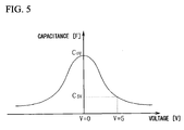
- the reason for this is that the higher the tunability, the greater the ability of a thin film capacitor to accommodate a broader resonance frequency band in response to smaller changes in voltage. More specifically, when the capacitance prior to application of voltage is defined as C 0V and the capacitance after a voltage tV has been applied is defined as C tV , then tunability is represented by (C 0V - C tV )/C tV x 100 (%).
- a tunable capacitor has been disclosed as an example of a technology for enhancing tunability in which high tunability is able to be ensured by using a material having a high dielectric constant while maintaining desired impedance during use in a high-frequency band (see, for example, Patent Document 2).
- Patent Document 2 ensures high tunability at low capacitance by forming a second dielectric layer having a lower dielectric constant than a first dielectric layer between the first dielectric layer and a top electrode so as to cover a portion of the principal surface of the first dielectric layer.
- Patent Document 3 describes a method for the preparation of a dielectric thin film with the composition Ba 0.7 Sr 0.3 TiO 3 . For the preparation of this thin film commercially available agents are used.
- the Patent Document 4 describes a further method for the preparation of a dielectric thin film.
- Patent Document 5 describes the preparation of a thin film from a composition consisting of barium n-butyrate, strontium n-butyrate and titanium isopropoxide.
- the inventors of the present invention determined that the microstructure observed in a film cross-section of a dielectric thin film is intimately related to the tunable properties of thin film capacitors.
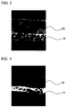
- a dielectric thin film 26 having a microstructure in which granular crystals having a large grain diameter are aggregated in a longitudinal cross-section of the film as shown in FIG 3 or a dielectric thin film 36 having a microstructure in which fine granular crystals are aggregated as shown in FIG. 4 , it tends to be difficult to obtain high tunability.
- An object of the present invention is to provide a process of forming a dielectric thin film capable of demonstrating high tunability in the case of being used in a thin film capacitor and the like, and that dielectric thin film.
- Another object of the present invention is to provide a thin film capacitor having high tunability and a tunable device provided with that thin film capacitor.
- a first aspect of the present invention is a process of forming a dielectric thin film having a composition consisting of Ba 1-x Sr x Ti y O 3 by coating and drying onto a support a composition for forming a Ba 1-x Sr x Ti y O 3 thin film, obtained by dissolving an organic barium compound, an organic strontium compound and a titanium alkoxide in an organic solvent at a molar ratio of Ba:Sr:Ti of 1-x:x:y, to form a coated film, followed by baking the support on which the coated film has been formed, wherein the process from coating to baking is carried out two to nine times, the thickness of the thin film formed after initial baking is 20 nm to 80 nm, the thickness of each thin film formed after the second baking and beyond is 20 nm to less than 200 nm, each baking from the first time to the second to ninth times is carried out by heating to a prescribed temperature within a range of 500°C to 800°C at a heating rate of 1°C to 50°C/
- the organic barium compound and the organic strontium compound each are a carboxylate that is a metal salt of a carboxylic acid represented by the general formula C n H 2n+1 COOH (wherein 3 ⁇ n ⁇ 7) and have the following structure
- R 1 to R 6 represent hydrogen atoms, methyl groups or ethyl groups
- M represents Ba or Sr.
- a second aspect of the present invention is a thin film capacitor having a substrate, an insulator film formed on the substrate, an adhesion layer formed on the insulator film, a lower electrode formed on the adhesion layer, a dielectric thin film formed according to the formation process of the first aspect on the lower electrode, and an upper electrode formed on the dielectric thin film, wherein the changing rate T of capacitance according to an applied voltage as indicated with the following formula (1) is 60% or more.
- T C 0 v ⁇ C 5 v / C 0 v ⁇ 100
- C 0V represents capacitance in the absence of an applied voltage
- C 5V represents capacitance during an applied voltage of 5 V.
- a third aspect of the present invention is a dielectric thin film formed according to the formation process of the first aspect that has a microstructure in which a plurality of columnar crystals are longitudinally arranged in the direction of thickness in a longitudinal cross-section thereof.
- a fourth aspect of the present invention is a tunable device provided with the thin film capacitor of the second aspect.
- the process from coating to baking is carried out two to nine times, the thickness of the thin film formed after the initial baking is 20 nm to 80 nm, and the thickness of each thin film formed after the second baking and beyond is 20 nm to less than 200 nm.
- each baking from the first time to the second to ninth times is carried out by heating to a prescribed temperature within the range of 500°C to 800°C at a heating rate of 1°C to 50°C/minute in an atmosphere at atmospheric pressure.
- the total thickness of the finally formed dielectric thin film is 100 nm to 600 nm, and the composition thereof is represented by Ba 1-x Sr x Ti y O 3 (0.2 ⁇ x ⁇ 0.6 and 0.9 ⁇ y ⁇ 1.1).
- a dielectric thin film can be formed that has a microstructure in which a plurality of columnar crystals are longitudinally arranged in the direction of thickness in a longitudinal cross-section of the film.
- a thin film capacitor and the like that is formed by using this dielectric thin film is able to demonstrate extremely high tunability.
- the thin film capacitor of the second aspect of the present invention allows the obtaining of extremely high tunability having a changing rate of capacitance in response to an applied voltage of 60% or more as a result of being provided with a dielectric thin film obtained according to the formation process of the present invention.
- the dielectric thin film of the third aspect of the present invention enables the demonstration of extremely high tunability in a thin film capacitor and the like formed by using that dielectric thin film that has a microstructure in which a plurality of columnar crystals are arranged longitudinally in the direction of thickness in a longitudinal cross-section of the film as a result of being formed according to the formation process of the present invention.
- the tunable device of the fourth aspect of the present invention allows the obtaining of extremely high tunable properties as a result of being provided with a tunable device in the form of the thin film capacitor of the present invention.
- the present invention demonstrates high tunability by forming a dielectric thin film used as a dielectric layer to have a desired microstructure in a thin film capacitor and the like.
- the desired microstructure refers to a microstructure in which a plurality of columnar crystals are longitudinally arranged in the direction of thickness in a longitudinal cross-section of the dielectric thin film 16 formed on a lower electrode 14 shown in FIG 2 .
- the dielectric thin film 16 having this microstructure is able to demonstrate high tunability in a thin film capacitor and the like formed by using this dielectric thin film 16 in comparison with the dielectric thin film 26 having a microstructure in which granular crystals having a large grain diameter are aggregated as shown in FIG. 3 or the dielectric thin film 36 having a microstructure in which fine granular crystals are aggregated as shown in FIG. 4 .
- the reason for this is presumed to be attributable to the increase in relative permittivity as the structure becomes larger.
- the microstructure of the present invention refers to a microstructure formed from, for example, a plurality of columnar crystals in each crystal grain is roughly mutually parallel in the lengthwise direction and perpendicular to the surface of the dielectric thin film.
- the dielectric thin film 16 having this microstructure can be formed by a so-called sol-gel method in which a composition for forming a thin film is coated and dried on a support to form a coated film followed by baking the support on which the coated film is formed.
- sol-gel method in which a composition for forming a thin film is coated and dried on a support to form a coated film followed by baking the support on which the coated film is formed.
- thin film capacitors consist of a three-layer type obtained by laminating the lower electrode 14, the dielectric thin film 16 and an upper electrode 17 on a substrate 11 in that order as shown in FIG. 1 , and a two-layer type not shown obtained by using an Si substrate having low specific resistance as a lower electrode and laminating a dielectric thin film and upper electrode thereon.
- the following provides an explanation of a thin film capacitor using the case of the former as an example.
- the substrate 11 examples include an Si substrate, and on an insulator film 12, a thermal oxide film (SiO 2 ) formed on the surface of this Si substrate by dry oxidation or wet oxidation in an oxidizing gas atmosphere.
- a precious metal such as platinum (Pt), for example, is used for the lower electrode 14, and this lower electrode 14 can be formed by a vapor phase growth method such as sputtering or vacuum deposition or by a screen printing method.
- an adhesion layer 13 may be suitably provided to ensure adhesion between the insulator film 12 and the lower electrode 14.
- a metal thin film having high oxidation affinity, such as that of Ti or Ta, or an oxide thereof, can be used for the adhesion layer 13.
- an example of the support on which the dielectric thin film 16 is formed is the substrate 11 having the insulator film 12 on which the adhesion layer 13 and lower electrode 14 are laminated, specific examples of which include Pt/Ti/SiO 2 /Si, Pt/IrO/Ir/SiO 2 /Si, Pt/TiN/SiO 2 /Si, Pt/Ta/SiO 2 /Si and Pt/Ir/SiO 2 /Si.
- an example of the composition for forming a thin film is a Ba 1-x Sr x Ti y O 3 composition for forming a thin film obtained by dissolving an organic barium compound, an organic strontium compound and a titanium alkoxide in an organic solvent so that the molar ratio of Ba:Sr:Ti is 1-x:x:y. Since the molar ratio in the composition is reflected in the molar ratio of the dielectric thin film following the formation thereof, the values of x and y are within the ranges of 0.2 ⁇ x ⁇ 0.6 and 0.9 ⁇ y ⁇ 1.1 for reasons to be subsequently described.
- a carboxylate that is a metal salt of a carboxylic acid represented by the general formula C n H 2n+1 COOH (where, 3 ⁇ n ⁇ 7) and is able to adopt the structure shown in the following formula (2) is used for the organic barium compound and the organic strontium compound.
- R 1 to R 6 represent hydrogen atoms, methyl groups or ethyl groups, and M represents Ba or Sr.
- the organic barium compound is particularly preferably barium 2-ethylhexanoate or barium 2-ethylbutyrate in consideration of availability of the raw materials.
- the organic strontium compound is particularly preferably strontium 2-ethylhexanoate or strontium 2-ethylbutyrate also in consideration of raw material availability.
- the titanium alkoxide is particularly preferably titanium isopropoxide or titanium butoxide again in consideration of raw material availability.
- This composition for forming a thin film is coated onto a support, namely the lower substrate 14 in this example. Continuing, the coated composition is dried to form a coated film followed by baking the support on which the coated film is formed to form the dielectric thin film 16 of a desired thickness on the lower electrode 14.
- the process from coating to baking is carried out two or more times in the present invention.
- the thickness of the thin film formed after the initial baking is 20 nm to 80 nm, while the thickness of each thin film formed after the second baking and beyond is 20 nm to less than 200 nm.
- the reason for carrying out the process from coating to baking two or more times is that if a thin film is formed to a desired film thickness in a single process, cracks form in the surface of the dielectric thin film due to differences in stress with the substrate and the like during baking, and for reasons to be subsequently described, the aforementioned desired microstructure consisting of columnar crystals is unable to be obtained.
- the reason for making the thickness of the thin film formed after the initial baking 80 nm or less is that, if a thick film is attempted be formed once on a lower electrode having different physical properties than those of the thin film, nuclei serving as starting points of crystal growth are formed not only at the electrode interface but also within the film during baking, and these nuclei facilitate the growth of granular crystals at the starting points, thereby preventing the obtaining of the desired columnar crystals.
- nuclei serving as starting points of crystal growth are not formed within the film and are preferentially formed in the vicinity of the interface with the lower electrode, thereby making it possible to form a microstructure consisting of columnar crystals.
- the desired microstructure consisting of columnar crystals can ultimately be obtained by using the initial thin film formed at the interface with the lower electrode in this manner as a seed layer, and successively growing columnar crystals by the process from coating to baking that is carried out repeatedly thereafter.
- the reason for making the thickness of the thin film formed after the initial baking 20 nm or more is that, if the thickness if less than 20 nm, hemispherical bulges of about 1 ⁇ m or less referred to as hillocks occur on the lower electrode during baking, and these hillocks cause problems in terms of leakage current and withstand voltage properties.
- the thickness of the thin film formed after initial baking is preferably 25 nm to 60 nm.
- the thin film can be grown into the desired microstructure consisting of columnar crystals even if the thickness of each thin film formed after the second baking and beyond is somewhat thick.
- the reason for limiting the thickness of each thin film formed after the second baking and beyond to the aforementioned range is that, if the thickness of each thin film is less then the lower limit value thereof, the number of processes from coating to baking becomes excessively large, thereby resulting in poor productivity.
- more of the hillocks described above are formed on the lower electrode, thereby creating problems in terms of leakage current and withstand voltage properties.
- the thickness of each thin film formed after the second baking and beyond is preferably 30 nm to 150 nm.
- the thickness of each thin film formed after the second baking and beyond is preferably equal to or greater than the film thickness of the thin film formed after the initial baking.
- the process from coating to baking is repeated two to nine times and preferably repeated 3 to 6 times.
- a conventional coating method such as spin coating, dip coating or spray coating can be preferably used to coat the composition for forming a thin film
- spin coating is used particularly preferably. Adjustment of film thickness is carried out by adjusting the rotating speed of spin coating and the viscosity of the composition for forming a thin film.
- Drying of the composition for forming a thin film that has been coated on the lower electrode 14 or a thin film formed after baking is preferably carried out within the range of room temperature to 350°C in an atmosphere at atmospheric pressure.
- thin film thickness is adjusted so that the thickness of each thin film after baking is within each of the aforementioned ranges.
- Each baking process from the initial baking to the second to ninth baking of the thin films formed by drying the coated composition for forming a thin film is carried out by heating to a prescribed temperature within the range of 500°C to 800°C at a heating rate of 1°C to 50°C/minute in an atmosphere at atmospheric pressure and preferably holding for 1 minute to 120 minutes.
- the reason for limiting the heating rate to the aforementioned range is that if the heating rate is below the lower limit value, the process ends up becoming extremely long, while on the other hand, if the heating rate exceeds the upper limit value, a microstructure composed of columnar crystals is unable to be obtained even if each film thickness after baking is set to the aforementioned ranges.
- the reason for limiting the prescribed temperature, namely the baking temperature, to the aforementioned range is that if the prescribed temperature is below the lower limit value, adequate crystallinity is unable to be obtained thereby preventing the obtaining of high tunability, while if the prescribed temperature exceeds the upper limit value, there is the risk of causing degeneration of the electrodes.
- Each drying and baking from the initial time to the final time may vary within the range of the aforementioned conditions even if the respective conditions are the same.
- Baking can be carried out at atmospheric pressure equivalent to an atmosphere at atmospheric pressure, and may be carried out, for example, in a nitrogen atmosphere at atmospheric pressure.
- the total thickness of the dielectric thin film formed by going through the processes described above is 100 nm to 600 nm.
- the reason for limiting the total thickness to the range of 100 nm to 600 nm is that if the total thickness is below the lower limit value, problems occur with respect to leakage current and withstand voltage properties.
- the total thickness of the dielectric thin film is preferably within the range of 250 nm to 450 nm.
- the values of x and y in the composition of the dielectric thin film, namely the dielectric thin film represented by Ba 1-x Sr x Ti y O 3 are such that 0.2 ⁇ x ⁇ 0.6 and 0.9 ⁇ y ⁇ 1.1.
- x is outside the aforementioned range, relative permittivity decreases and becomes inadequate.
- y is outside the aforementioned range, tunability decreases.
- the values of x and y are preferably such that 0.25 ⁇ x ⁇ 0.55 and 0.95 ⁇ y ⁇ 1.05.
- the upper electrode 17 is laminated onto the dielectric thin film 16 to obtain a thin film capacitor. Similar to the aforementioned lower electrode 14, a precious metal such as Pt is also used for the upper electrode 17, and the upper electrode 17 can be formed by a vapor phase growth method such as sputtering or vacuum deposition or by a screen printing method. Furthermore, the composition of the thin film capacitor is not limited to the composition shown in the example.
- a thin film capacitor having the dielectric thin film of the present invention allows the obtaining of high tunability as a result of the dielectric thin film having a desired microstructure consisting of columnar crystals in a longitudinal cross-section of the film.
- the range of a capacitance C 0V in the absence of an applied voltage to a capacitance C 5V during application of an applied voltage of 5 V can be made to be larger than that of the prior art.
- a thin film capacitor formed by using the dielectric thin film of the present invention has various superior properties, including tunability, and can be applied to high-frequency tunable devices such as high-frequency filters, high-frequency antennas or phase shifters.
- a substrate 11 was prepared in which the adhesion layer 13 and the Pt lower electrode 14 were laminated on the insulator film 12.
- barium 2-ethylhexanoate as organic barium compound, strontium 2-ethylhexanoate as organic strontium compound, and titanium isopropoxide as titanium alkoxide were prepared, and these were dissolved in isoamyl acetate so that the molar ratio of Ba, Sr and Ti was 45:55:100 to prepare a composition for forming a thin film.
- the coated film was heated to 700°C at a heating rate of 5°C/min in air followed by holding at this temperature (baking temperature) for 60 minutes to form a thin film having a thickness of 80 nm.
- the process from coating to baking was carried out a total of four times, including the initial coating and baking, under the same conditions as described above to form the dielectric thin film 16 on the Pt lower electrode 14 such that the molar ratio of Ba, Sr and Ti of the dielectric thin film 16 was 45:55:100 and the total thickness thereof was 320 nm. Furthermore, the thickness of each thin film formed after the second baking and beyond was 80 nm in all cases.
- Example 1 the Pt upper electrode 17 measuring about 250 ⁇ m x 250 ⁇ m square was formed on the formed dielectric thin film 16 by sputtering method using a metal mask to obtain a thin film capacitor.
- This thin film capacitor was designated as Example 1.
- a thin film capacitor was obtained in the same manner as Example 1 with the exception of making the molar ratio of Ba, Sr and Ti in the composition for forming a thin film, namely the molar ratio of Ba, Sr and Ti in the dielectric thin film after forming, to be 50:50:100.
- This thin film capacitor was designated as Example 2.
- a thin film capacitor was obtained in the same manner as Example 1 with the exception of making the molar ratio of Ba, Sr and Ti in the composition for forming a thin film, namely the molar ratio of Ba, Sr and Ti in the dielectric thin film after forming, to be 70:30:100.
- This thin film capacitor was designated as Example 3.
- a thin film capacitor was obtained in the same manner as Example 1 with the exception of making the molar ratio of Ba, Sr and Ti in the composition for forming a thin film, namely the molar ratio of Ba, Sr and Ti in the dielectric thin film after forming, to be 75:25:100.
- This thin film capacitor was designated as Example 4.
- a thin film capacitor was obtained in the same manner as Example 1 with the exception of making the molar ratio of Ba, Sr and Ti in the composition for forming a thin film, namely the molar ratio of Ba, Sr and Ti in the dielectric thin film after forming, to be 70:35:95.
- This thin film capacitor was designated as Example 5.
- a thin film capacitor was obtained in the same manner as Example 1 with the exception of making the molar ratio of Ba, Sr and Ti in the composition for forming a thin film, namely the molar ratio of Ba, Sr and Ti in the dielectric thin film after forming, to be 70:30:105.
- This thin film capacitor was designated as Example 6.
- a thin film capacitor was obtained in the same manner as Example 3 with the exception of making the thickness of the thin film formed after the initial baking to be 40 nm, making the thickness of each thin film formed after the second baking and beyond to be 40 nm, and carrying out the process from coating to baking a total of 8 times, including the initial coating and baking.
- This thin film capacitor was designated as Example 7.
- a thin film capacitor was obtained in the same manner as Example 3 with the exception of making the thickness of the thin film formed after the initial baking to be 80 nm, making the thickness of each thin film formed after the second baking and beyond to be 120 nm, and carrying out the process from coating to baking a total of 3 times, including the initial coating and baking.
- This thin film capacitor was designated as Example 8.
- a thin film capacitor was obtained in the same manner as Example 3 with the exception of making the thickness of the thin film formed after the initial baking to be 80 nm, making the thickness of each thin film formed after the second baking and beyond to be 80 nm, carrying out the process from coating to baking a total of 2 times, including the initial coating and baking, and forming a dielectric thin film having a total thickness of 160 nm.
- This thin film capacitor was designated as Example 9.
- a thin film capacitor was obtained in the same manner as Example 3 with the exception of making the heating rate during baking to be 30°C/minute. This thin film capacitor was designated as Example 10.
- a thin film capacitor was obtained in the same manner as Example 3 with the exception of making the baking temperature to be 500°C. This thin film capacitor was designated as Example 11.
- a thin film capacitor was obtained in the same manner as Example 3 with the exception of making the baking temperature to be 600°C. This thin film capacitor was designated as Example 12.
- a thin film capacitor was obtained in the same manner as Example 3 with the exception of making the baking temperature to be 800°C. This thin film capacitor was designated as Example 13.
- a thin film capacitor was obtained in the same manner as Example 1 with the exception of preparing the composition for forming a thin film using barium 2-ethylbutyrate for the organic barium compound and using strontium 2-ethylbutyrate for the organic strontium compound.
- This thin film capacitor was designated as Example 14.
- Example 15 A thin film capacitor was obtained in the same manner as Example 1 with the exception of carrying out baking in a nitrogen gas atmosphere at atmospheric pressure. This thin film capacitor was designated as Example 15.
- Example 16 A thin film capacitor was obtained in the same manner as Example 2 with the exception of carrying out baking in a nitrogen gas atmosphere at atmospheric pressure. This thin film capacitor was designated as Example 16.
- Example 17 A thin film capacitor was obtained in the same manner as Example 3 with the exception of carrying out baking in a nitrogen gas atmosphere at atmospheric pressure. This thin film capacitor was designated as Example 17.
- Example 18 A thin film capacitor was obtained in the same manner as Example 4 with the exception of carrying out baking in a nitrogen gas atmosphere at atmospheric pressure. This thin film capacitor was designated as Example 18.
- Example 19 A thin film capacitor was obtained in the same manner as Example 5 with the exception of carrying out baking in a nitrogen gas atmosphere at atmospheric pressure. This thin film capacitor was designated as Example 19.
- Example 20 A thin film capacitor was obtained in the same manner as Example 6 with the exception of carrying out baking in a nitrogen gas atmosphere at atmospheric pressure. This thin film capacitor was designated as Example 20.
- Example 21 A thin film capacitor was obtained in the same manner as Example 7 with the exception of carrying out baking in a nitrogen gas atmosphere at atmospheric pressure. This thin film capacitor was designated as Example 21.
- Example 22 A thin film capacitor was obtained in the same manner as Example 8 with the exception of carrying out baking in a nitrogen gas atmosphere at atmospheric pressure. This thin film capacitor was designated as Example 22.
- Example 23 A thin film capacitor was obtained in the same manner as Example 9 with the exception of carrying out baking in a nitrogen gas atmosphere at atmospheric pressure. This thin film capacitor was designated as Example 23.
- Example 24 A thin film capacitor was obtained in the same manner as Example 10 with the exception of carrying out baking in a nitrogen gas atmosphere at atmospheric pressure. This thin film capacitor was designated as Example 24.
- Example 25 A thin film capacitor was obtained in the same manner as Example 11 with the exception of carrying out baking in a nitrogen gas atmosphere at atmospheric pressure. This thin film capacitor was designated as Example 25.
- Example 26 A thin film capacitor was obtained in the same manner as Example 12 with the exception of carrying out baking in a nitrogen gas atmosphere at atmospheric pressure. This thin film capacitor was designated as Example 26.
- Example 27 A thin film capacitor was obtained in the same manner as Example 13 with the exception of carrying out baking in a nitrogen gas atmosphere at atmospheric pressure. This thin film capacitor was designated as Example 27.
- Example 28 A thin film capacitor was obtained in the same manner as Example 14 with the exception of carrying out baking in a nitrogen gas atmosphere at atmospheric pressure. This thin film capacitor was designated as Example 28.
- a thin film capacitor was obtained in the same manner as Example 1 with the exception of making the molar ratio of Ba, Sr and Ti in the composition for forming a thin film, namely the molar ratio of Ba, Sr and Ti in the dielectric thin film after forming, to be 10:90:100.
- This thin film capacitor was designated as Comparative Example 1.
- a thin film capacitor was obtained in the same manner as Example 1 with the exception of making the molar ratio of Ba, Sr and Ti in the composition for forming a thin film, namely the molar ratio of Ba, Sr and Ti in the dielectric thin film after forming, to be 30:70:100.
- This thin film capacitor was designated as Comparative Example 2.
- a thin film capacitor was obtained in the same manner as Example 1 with the exception of making the molar ratio of Ba, Sr and Ti in the composition for forming a thin film, namely the molar ratio of Ba, Sr and Ti in the dielectric thin film after forming, to be 90:10:100.
- This thin film capacitor was designated as Comparative Example 3.
- a thin film capacitor was obtained in the same manner as Example 1 with the exception of making the molar ratio of Ba, Sr and Ti in the composition for forming a thin film, namely the molar ratio of Ba, Sr and Ti in the dielectric thin film after forming, to be 100:0:100.
- This thin film capacitor was designated as Comparative Example 4.
- a thin film capacitor was obtained in the same manner as Example 3 with the exception of making the thickness of the thin film formed after the initial baking to be 10 nm, making the thickness of each thin film formed after the second baking and beyond to be 10 nm, and carrying out the process from coating to baking a total of 32 times, including the initial coating and baking.
- This thin film capacitor was designated as Comparative Example 5.
- a thin film capacitor was obtained in the same manner as Example 3 with the exception of making the thickness of the thin film formed after the initial baking to be 160 nm, making the thickness of each thin film formed after the second baking and beyond to be 160 nm, and carrying out the process from coating to baking a total of 2 times, including the initial coating and baking.
- This thin film capacitor was designated as Comparative Example 6.
- a thin film capacitor was obtained in the same manner as Example 3 with the exception of making the thickness of the thin film formed after the initial baking to be 320 nm, and carrying out the process from coating to baking a total of 1 time.
- This thin film capacitor was designated as Comparative Example 7.
- a thin film capacitor was obtained in the same manner as Example 3 with the exception of carrying out the process from coating to baking a total of 10 times, including the initial coating and baking, and forming a dielectric thin film having a total thickness of 800 nm.
- This thin film capacitor was designated as Comparative Example 8.
- a thin film capacitor was obtained in the same manner as Example 3 with the exception of making the thickness of the thin film formed after the initial baking to be 80 nm, carrying out the process from coating to baking a total of 1 time, and forming a dielectric thin film having a total thickness of 80 nm.
- This thin film capacitor was designated as Comparative Example 9.
- a thin film capacitor was obtained in the same manner as Example 3 with the exception of making the heating rate during baking to be 60°C/minute. This thin film capacitor was designated as Comparative Example 10.
- a thin film capacitor was obtained in the same manner as Example 3 with the exception of making the heating rate during baking to be 100°C/minute. This thin film capacitor was designated as Comparative Example 11.
- a thin film capacitor was obtained in the same manner as Example 3 with the exception of making the heating rate during baking to be 600°C/minute. This thin film capacitor was designated as Comparative Example 12.
- a thin film capacitor was obtained in the same manner as Example 3 with the exception of making the baking temperature to be 450°C. This thin film capacitor was designated as Comparative Example 13.
- a thin film capacitor was obtained in the same manner as Example 3 with the exception of making the baking temperature to be 900°C. This thin film capacitor was designated as Comparative Example 14.
- a thin film capacitor was obtained in the same manner as Comparative Example 1 with the exception of carrying out baking in a nitrogen gas atmosphere at atmospheric pressure. This thin film capacitor was designated as Comparative Example 15.
- a thin film capacitor was obtained in the same manner as Comparative Example 2 with the exception of carrying out baking in a nitrogen gas atmosphere at atmospheric pressure. This thin film capacitor was designated as Comparative Example 16.
- a thin film capacitor was obtained in the same manner as Comparative Example 3 with the exception of carrying out baking in a nitrogen gas atmosphere at atmospheric pressure. This thin film capacitor was designated as Comparative Example 17.
- a thin film capacitor was obtained in the same manner as Comparative Example 4 with the exception of carrying out baking in a nitrogen gas atmosphere at atmospheric pressure. This thin film capacitor was designated as Comparative Example 18.
- a thin film capacitor was obtained in the same manner as Comparative Example 5 with the exception of carrying out baking in a nitrogen gas atmosphere at atmospheric pressure. This thin film capacitor was designated as Comparative Example 19.
- a thin film capacitor was obtained in the same manner as Comparative Example 6 with the exception of carrying out baking in a nitrogen gas atmosphere at atmospheric pressure. This thin film capacitor was designated as Comparative Example 20.
- a thin film capacitor was obtained in the same manner as Comparative Example 7 with the exception of carrying out baking in a nitrogen gas atmosphere at atmospheric pressure. This thin film capacitor was designated as Comparative Example 21.
- a thin film capacitor was obtained in the same manner as Comparative Example 8 with the exception of carrying out baking in a nitrogen gas atmosphere at atmospheric pressure. This thin film capacitor was designated as Comparative Example 22.
- a thin film capacitor was obtained in the same manner as Comparative Example 9 with the exception of carrying out baking in a nitrogen gas atmosphere at atmospheric pressure. This thin film capacitor was designated as Comparative Example 23.
- a thin film capacitor was obtained in the same manner as Comparative Example 10 with the exception of carrying out baking in a nitrogen gas atmosphere at atmospheric pressure. This thin film capacitor was designated as Comparative Example 24.
- a thin film capacitor was obtained in the same manner as Comparative Example 11 with the exception of carrying out baking in a nitrogen gas atmosphere at atmospheric pressure. This thin film capacitor was designated as Comparative Example 25.
- a thin film capacitor was obtained in the same manner as Comparative Example 12 with the exception of carrying out baking in a nitrogen gas atmosphere at atmospheric pressure. This thin film capacitor was designated as Comparative Example 26.
- a thin film capacitor was obtained in the same manner as Comparative Example 13 with the exception of carrying out baking in a nitrogen gas atmosphere at atmospheric pressure. This thin film capacitor was designated as Comparative Example 27.
- a thin film capacitor was obtained in the same manner as Comparative Example 14 with the exception of carrying out baking in a nitrogen gas atmosphere at atmospheric pressure. This thin film capacitor was designated as Comparative Example 28.
- a voltage up to 5 V was applied at a frequency of 1 MHz and at a temperature of 23°C between the Pt lower electrode and the Pt upper electrode of the thin film capacitors, and the changing rate T of capacitance as calculated from the following formula (1) was measured from a capacitance C 0V when the voltage was not applied and a capacitance C 5V when a voltage of 5 V was applied. Furthermore, the capacitance changing rate T was measured using an impedance material analyzer (Hewlett-Packard, Model HP4291 A).
- Comparative Example 5 in which the thickness of the thin film formed after the initial baking was less than 20 nm and the process from coating to baking was carried out in excess of 9 times, hillocks formed and adequate withstand voltage was unable to be obtained due to the presence of these hillocks.
- Comparative Example 6 in which the thickness of the thin film formed after the initial baking exceeded 80 nm, and in Comparative Example 7, in which the dielectric thin film was formed in a single process from coating to baking, the desired columnar crystals were not obtained resulting in low tunability.
- Comparative Example 8 in which the total thickness of the dielectric thin film exceeded 600 nm, high relative permittivity was unable to be obtained, and as a result thereof, adequate tunability was unable to be obtained.
- Comparative Example 9 in which the total thickness was less than 100 nm and the dielectric thin film was formed with a single process from coating to baking, adequate withstand voltage was unable to be obtained.
- Comparative Example 13 in which baking was carried out a baking temperature below 500°C, adequate tunability was unable to be obtained as a result of not obtaining adequate crystallinity, while in Comparative Example 14, in which baking was carried out at a baking temperature above 800°C, although high tunability was obtained, this resulted in the occurrence of degeneration of the Pt lower electrode.
Landscapes
- Engineering & Computer Science (AREA)
- Chemical & Material Sciences (AREA)
- Power Engineering (AREA)
- Ceramic Engineering (AREA)
- Manufacturing & Machinery (AREA)
- Microelectronics & Electronic Packaging (AREA)
- Materials Engineering (AREA)
- Organic Chemistry (AREA)
- Inorganic Chemistry (AREA)
- Computer Hardware Design (AREA)
- Structural Engineering (AREA)
- Condensed Matter Physics & Semiconductors (AREA)
- General Physics & Mathematics (AREA)
- Physics & Mathematics (AREA)
- Dispersion Chemistry (AREA)
- Life Sciences & Earth Sciences (AREA)
- Environmental & Geological Engineering (AREA)
- General Life Sciences & Earth Sciences (AREA)
- Geology (AREA)
- Fixed Capacitors And Capacitor Manufacturing Machines (AREA)
- Ceramic Capacitors (AREA)
- Inorganic Insulating Materials (AREA)
- Compositions Of Oxide Ceramics (AREA)
- Inorganic Compounds Of Heavy Metals (AREA)
Claims (4)
- Procédé de formation d'un film mince diélectrique comprenant le fait :de préparer une composition constituée de Ba1-xSrxTiyO3 obtenue par dissolution d'un composé de baryum organique, d'un composé de strontium organique et d'un alcoxyde de titane dans un solvant organique à un rapport molaire de Ba : Sr : Ti de 1-x : x : y ;de déposer et de sécher sur un support, la composition pour former un film déposé ; etde cuire le support sur lequel le film déposé a été formé afin de former un film mince de Ba1-xSrxTiyO3, oùle procédé depuis le dépôt jusqu'à la cuisson est effectué deux à neuf fois,l'épaisseur du film mince formé après la cuisson initiale est comprise entre 20 nm et 80 nm,l'épaisseur de chaque film mince formé après la deuxième cuisson et au-delà est supérieure ou égale à 20 nm et inférieure à 200 nm,chaque cuisson depuis la première fois jusqu'à la deuxième à la neuvième fois est effectuée par chauffage à une température prescrite se trouvant dans une plage allant de 500°C à 800°C à une vitesse de chauffage allant de 1 °C à 50°C/minute dans une atmosphère à pression atmosphérique,l'épaisseur totale du film mince diélectrique est comprise entre 100 nm et 600 nm,les valeurs de x et y indiquant la composition du film mince diélectrique sont telles que 0,2 < x < 0,6 et 0,9 < y < 1,1,le composé de baryum organique et le composé de strontium organique sont des sels métalliques d'un acide carboxylique représenté par la formule générale CnH2n+1COOH moyennant quoi 3 ≤ n ≤ 7 ; etles sels métalliques de l'acide carboxylique présentent une structure représentée dans la formule (2) suivante :

- Condensateur à film mince comprenant :un substrat ;un film isolant formé sur le substrat ;une couche d'adhérence formée sur le film isolant ;une électrode inférieure formée sur la couche d'adhérence ;un film mince diélectrique formé par le procédé de formation selon la revendication 1 sur l'électrode inférieure ; etune électrode supérieure formée sur le film mince diélectrique, oùle taux de variation T de capacité selon une tension appliquée comme l'indique la formule (1) suivante est supérieur ou égal à 60% :

- Film mince diélectrique formé par le procédé de formation selon la revendication 1 comprenant :une microstructure dans laquelle une pluralité de cristaux en colonnes sont agencés longitudinalement dans la direction de l'épaisseur dans une section longitudinale de celui-ci.
- Dispositif accordable comprenant :le condensateur à film mince selon la revendication 2.
Applications Claiming Priority (2)
| Application Number | Priority Date | Filing Date | Title |
|---|---|---|---|
| JP2009202474 | 2009-09-02 | ||
| PCT/JP2010/065059 WO2011027833A1 (fr) | 2009-09-02 | 2010-09-02 | Procédé de formation d'une couche mince diélectrique et condensateur en couches minces comprenant la couche mince diélectrique |
Publications (3)
| Publication Number | Publication Date |
|---|---|
| EP2474505A1 EP2474505A1 (fr) | 2012-07-11 |
| EP2474505A4 EP2474505A4 (fr) | 2013-03-20 |
| EP2474505B1 true EP2474505B1 (fr) | 2016-07-27 |
Family
ID=43649367
Family Applications (1)
| Application Number | Title | Priority Date | Filing Date |
|---|---|---|---|
| EP10813781.1A Active EP2474505B1 (fr) | 2009-09-02 | 2010-09-02 | Procédé de formation d'une couche mince diélectrique et condensateur en couches minces comprenant ladite couche mince diélectrique |
Country Status (7)
| Country | Link |
|---|---|
| US (1) | US8891227B2 (fr) |
| EP (1) | EP2474505B1 (fr) |
| JP (1) | JP5617441B2 (fr) |
| KR (1) | KR101759361B1 (fr) |
| CN (1) | CN102482115A (fr) |
| IN (1) | IN2012DN02314A (fr) |
| WO (1) | WO2011027833A1 (fr) |
Families Citing this family (6)
| Publication number | Priority date | Publication date | Assignee | Title |
|---|---|---|---|---|
| KR101452186B1 (ko) * | 2012-12-26 | 2014-10-21 | 주식회사 누리비스타 | 내부 전극용 페이스트 및 이를 이용하여 제조된 적층형 세라믹 전자 부품 |
| JP2014144881A (ja) * | 2013-01-28 | 2014-08-14 | Mitsubishi Materials Corp | 誘電体薄膜形成用組成物及びこの組成物を用いた誘電体薄膜の形成方法 |
| CN105006362B (zh) * | 2015-07-28 | 2018-06-19 | 桂林电子科技大学 | 一种可剥离衬底的薄膜电容器制备方法 |
| KR101813374B1 (ko) * | 2016-05-13 | 2017-12-28 | 삼성전기주식회사 | 박막 커패시터 및 그 제조방법 |
| US10479732B2 (en) * | 2017-03-31 | 2019-11-19 | Tdk Corporation | Oxynitride thin film and capacitance element |
| HRP20231014T1 (hr) * | 2018-07-30 | 2023-12-08 | Digital Concepts Company Limited | Upravljivi kondenzator i postupak njegovog upravljanja i proizvodnje |
Family Cites Families (19)
| Publication number | Priority date | Publication date | Assignee | Title |
|---|---|---|---|---|
| JPS60236404A (ja) | 1984-05-10 | 1985-11-25 | 日本曹達株式会社 | 薄膜強誘電体の製造方法 |
| JPH01308801A (ja) | 1988-06-08 | 1989-12-13 | Murata Mfg Co Ltd | 誘電体薄膜の製造方法 |
| US5005102A (en) * | 1989-06-20 | 1991-04-02 | Ramtron Corporation | Multilayer electrodes for integrated circuit capacitors |
| US6174564B1 (en) * | 1991-12-13 | 2001-01-16 | Symetrix Corporation | Method of making metal polyoxyalkylated precursor solutions |
| JP3007795B2 (ja) * | 1994-06-16 | 2000-02-07 | シャープ株式会社 | 複合金属酸化物誘電体薄膜の製造方法 |
| JP3446461B2 (ja) * | 1995-06-09 | 2003-09-16 | 三菱マテリアル株式会社 | Ba1−xSrxTiyO3薄膜形成用組成物、Ba1−xSrxTiyO3薄膜の形成方法及び薄膜コンデンサの製造方法 |
| KR100406665B1 (ko) * | 1995-06-09 | 2004-03-26 | 미쓰비시 마테리알 가부시키가이샤 | Ba1-xSrxTiyO3 박막 형성용 조성물 및 Ba1-xSrxTiyO3 박막의 형성방법 |
| JP3178303B2 (ja) * | 1995-06-23 | 2001-06-18 | 三菱マテリアル株式会社 | Ba1−xSrxTiyO3薄膜形成用組成物及びBa1−xSrxTiyO3薄膜の形成方法 |
| JPH0978249A (ja) | 1995-09-14 | 1997-03-25 | Fujitsu Ltd | 誘電体薄膜の作製方法 |
| CN1049644C (zh) | 1997-03-21 | 2000-02-23 | 中国科学院上海硅酸盐研究所 | 用水为溶剂的前驱物溶液制备钛酸锶钡薄膜的方法 |
| JP3599558B2 (ja) * | 1998-03-10 | 2004-12-08 | シャープ株式会社 | 高周波用容量可変素子の製造方法及び高周波用容量可変素子 |
| JP4048650B2 (ja) | 1999-06-07 | 2008-02-20 | 三菱マテリアル株式会社 | ペロブスカイト型酸化物薄膜形成用原料溶液 |
| US6803134B1 (en) | 2002-05-31 | 2004-10-12 | The United States Of America As Represented By The Secretary Of The Army | Paraelectric thin film material and method statement of government interest |
| WO2005089051A2 (fr) | 2004-03-15 | 2005-09-29 | Energenius, Inc. | Composants micro-ondes ferroelectriques a film mince et dispositifs sur substrats en feuille metallique souples |
| KR100861959B1 (ko) | 2005-04-28 | 2008-10-09 | 미쓰이 긴조꾸 고교 가부시키가이샤 | 산화물 유전층의 형성 방법 및 그 형성 방법으로 얻어진산화물 유전층을 구비한 커패시터층 형성재 |
| JP3958343B2 (ja) | 2005-04-28 | 2007-08-15 | 三井金属鉱業株式会社 | 酸化物誘電層の形成方法及びその形成方法で得られた酸化物誘電層を備えたキャパシタ層形成材 |
| JP2007019432A (ja) * | 2005-07-11 | 2007-01-25 | Tokyo Ohka Kogyo Co Ltd | 常誘電体薄膜およびその形成方法 |
| JP4907266B2 (ja) * | 2006-08-25 | 2012-03-28 | 太陽誘電株式会社 | チューナブルキャパシタ |
| JP2009202474A (ja) | 2008-02-28 | 2009-09-10 | Toshiba Tec Corp | インクジェット記録装置 |
-
2010
- 2010-08-30 JP JP2010192655A patent/JP5617441B2/ja active Active
- 2010-09-02 CN CN2010800389132A patent/CN102482115A/zh active Pending
- 2010-09-02 WO PCT/JP2010/065059 patent/WO2011027833A1/fr active Application Filing
- 2010-09-02 IN IN2314DEN2012 patent/IN2012DN02314A/en unknown
- 2010-09-02 KR KR1020127008343A patent/KR101759361B1/ko active IP Right Grant
- 2010-09-02 US US13/393,908 patent/US8891227B2/en active Active
- 2010-09-02 EP EP10813781.1A patent/EP2474505B1/fr active Active
Also Published As
| Publication number | Publication date |
|---|---|
| JP2011073960A (ja) | 2011-04-14 |
| EP2474505A4 (fr) | 2013-03-20 |
| US8891227B2 (en) | 2014-11-18 |
| IN2012DN02314A (fr) | 2015-08-21 |
| JP5617441B2 (ja) | 2014-11-05 |
| WO2011027833A1 (fr) | 2011-03-10 |
| EP2474505A1 (fr) | 2012-07-11 |
| KR101759361B1 (ko) | 2017-07-18 |
| KR20120059596A (ko) | 2012-06-08 |
| US20120224297A1 (en) | 2012-09-06 |
| CN102482115A (zh) | 2012-05-30 |
Similar Documents
| Publication | Publication Date | Title |
|---|---|---|
| EP2474505B1 (fr) | Procédé de formation d'une couche mince diélectrique et condensateur en couches minces comprenant ladite couche mince diélectrique | |
| TWI613725B (zh) | 強介電體薄膜之製造方法 | |
| JP4935674B2 (ja) | 薄膜コンデンサの製造方法 | |
| EP2431986B1 (fr) | Composition pour la formation de film mince diélectrique, procédé de formation de film mince diélectrique et film mince diélectrique ainsi formé | |
| WO2005083726A1 (fr) | Composites ferroelectriques en film mince, leur procede de fabrication et condensateur en etant fait | |
| EP1780305B1 (fr) | Film diélectrique et procedé de fabrication | |
| EP2402982B1 (fr) | Procédé de fabrication d'un condensateur à film mince et condensateur à film mince ainsi obtenu | |
| JP2008109082A (ja) | コンデンサのための同時焼成電極を有する薄膜誘電体、およびその製造方法 | |
| KR102111825B1 (ko) | 강유전체막이 부착된 실리콘 기판 | |
| CN103979617B (zh) | LaNiO3薄膜形成用组合物及使用该组合物的LaNiO3薄膜的形成方法 | |
| US20100206215A1 (en) | Method for producing single-crystal thin film | |
| JP3681844B2 (ja) | 誘電体薄膜及びセラミックコンデンサ | |
| EP3041032B1 (fr) | Composition de formation de film mince de lanio3, et procédé de formation d'un film mince de lanio3 dans lequel ladite composition est utilisée | |
| JP5531853B2 (ja) | 薄膜キャパシタの製造方法及び該方法により得られた薄膜キャパシタ | |
| JP3481807B2 (ja) | 誘電体薄膜およびセラミックコンデンサ | |
| JP3215030B2 (ja) | 誘電体薄膜 | |
| US6921671B1 (en) | Buffer layers to enhance the C-axis growth of Bi4Ti3O12 thin film on high temperature iridium-composite electrode | |
| JPH08330179A (ja) | セラミックコンデンサ | |
| JPH09293629A (ja) | 薄膜コンデンサ | |
| JPH0528831A (ja) | 薄膜誘電体およびその製造方法 | |
| JP2008004576A (ja) | 誘電体薄膜形成用基板の前処理方法 | |
| JPH04328817A (ja) | 電極付きセラミック薄膜の製造方法 | |
| JPH06215630A (ja) | 薄膜状誘電体及びその製造方法 | |
| JPH1149567A (ja) | 誘電体薄膜およびセラミックコンデンサ | |
| JPH1143371A (ja) | 誘電体薄膜およびセラミックコンデンサ |
Legal Events
| Date | Code | Title | Description |
|---|---|---|---|
| PUAI | Public reference made under article 153(3) epc to a published international application that has entered the european phase |
Free format text: ORIGINAL CODE: 0009012 |
|
| 17P | Request for examination filed |
Effective date: 20120307 |
|
| AK | Designated contracting states |
Kind code of ref document: A1 Designated state(s): AL AT BE BG CH CY CZ DE DK EE ES FI FR GB GR HR HU IE IS IT LI LT LU LV MC MK MT NL NO PL PT RO SE SI SK SM TR |
|
| DAX | Request for extension of the european patent (deleted) | ||
| A4 | Supplementary search report drawn up and despatched |
Effective date: 20130219 |
|
| RIC1 | Information provided on ipc code assigned before grant |
Ipc: H01G 4/12 20060101ALI20130213BHEP Ipc: C04B 35/468 20060101ALI20130213BHEP Ipc: C04B 35/624 20060101ALI20130213BHEP Ipc: C04B 35/47 20060101ALI20130213BHEP Ipc: C01G 23/00 20060101AFI20130213BHEP Ipc: H01G 7/06 20060101ALI20130213BHEP Ipc: C04B 35/46 20060101ALI20130213BHEP Ipc: H01G 4/33 20060101ALI20130213BHEP Ipc: H01L 21/02 20060101ALI20130213BHEP Ipc: B32B 18/00 20060101ALI20130213BHEP |
|
| 17Q | First examination report despatched |
Effective date: 20131125 |
|
| REG | Reference to a national code |
Ref country code: DE Ref legal event code: R079 Ref document number: 602010035100 Country of ref document: DE Free format text: PREVIOUS MAIN CLASS: C01G0023000000 Ipc: C04B0035468000 |
|
| GRAP | Despatch of communication of intention to grant a patent |
Free format text: ORIGINAL CODE: EPIDOSNIGR1 |
|
| RIC1 | Information provided on ipc code assigned before grant |
Ipc: C04B 35/47 20060101ALI20160127BHEP Ipc: H01L 49/02 20060101ALI20160127BHEP Ipc: H01G 4/33 20060101ALI20160127BHEP Ipc: H01L 21/02 20060101ALI20160127BHEP Ipc: H01G 7/06 20060101ALI20160127BHEP Ipc: C01G 23/00 20060101ALI20160127BHEP Ipc: C04B 35/468 20060101AFI20160127BHEP Ipc: C04B 35/624 20060101ALI20160127BHEP Ipc: H01G 4/12 20060101ALI20160127BHEP |
|
| INTG | Intention to grant announced |
Effective date: 20160229 |
|
| GRAS | Grant fee paid |
Free format text: ORIGINAL CODE: EPIDOSNIGR3 |
|
| GRAA | (expected) grant |
Free format text: ORIGINAL CODE: 0009210 |
|
| AK | Designated contracting states |
Kind code of ref document: B1 Designated state(s): AL AT BE BG CH CY CZ DE DK EE ES FI FR GB GR HR HU IE IS IT LI LT LU LV MC MK MT NL NO PL PT RO SE SI SK SM TR |
|
| REG | Reference to a national code |
Ref country code: GB Ref legal event code: FG4D |
|
| REG | Reference to a national code |
Ref country code: CH Ref legal event code: EP |
|
| REG | Reference to a national code |
Ref country code: AT Ref legal event code: REF Ref document number: 815663 Country of ref document: AT Kind code of ref document: T Effective date: 20160815 |
|
| REG | Reference to a national code |
Ref country code: IE Ref legal event code: FG4D |
|
| REG | Reference to a national code |
Ref country code: DE Ref legal event code: R096 Ref document number: 602010035100 Country of ref document: DE |
|
| REG | Reference to a national code |
Ref country code: FR Ref legal event code: PLFP Year of fee payment: 7 |
|
| REG | Reference to a national code |
Ref country code: LT Ref legal event code: MG4D |
|
| REG | Reference to a national code |
Ref country code: NL Ref legal event code: MP Effective date: 20160727 |
|
| REG | Reference to a national code |
Ref country code: AT Ref legal event code: MK05 Ref document number: 815663 Country of ref document: AT Kind code of ref document: T Effective date: 20160727 |
|
| PG25 | Lapsed in a contracting state [announced via postgrant information from national office to epo] |
Ref country code: FI Free format text: LAPSE BECAUSE OF FAILURE TO SUBMIT A TRANSLATION OF THE DESCRIPTION OR TO PAY THE FEE WITHIN THE PRESCRIBED TIME-LIMIT Effective date: 20160727 Ref country code: HR Free format text: LAPSE BECAUSE OF FAILURE TO SUBMIT A TRANSLATION OF THE DESCRIPTION OR TO PAY THE FEE WITHIN THE PRESCRIBED TIME-LIMIT Effective date: 20160727 Ref country code: NL Free format text: LAPSE BECAUSE OF FAILURE TO SUBMIT A TRANSLATION OF THE DESCRIPTION OR TO PAY THE FEE WITHIN THE PRESCRIBED TIME-LIMIT Effective date: 20160727 Ref country code: IS Free format text: LAPSE BECAUSE OF FAILURE TO SUBMIT A TRANSLATION OF THE DESCRIPTION OR TO PAY THE FEE WITHIN THE PRESCRIBED TIME-LIMIT Effective date: 20161127 Ref country code: NO Free format text: LAPSE BECAUSE OF FAILURE TO SUBMIT A TRANSLATION OF THE DESCRIPTION OR TO PAY THE FEE WITHIN THE PRESCRIBED TIME-LIMIT Effective date: 20161027 Ref country code: LT Free format text: LAPSE BECAUSE OF FAILURE TO SUBMIT A TRANSLATION OF THE DESCRIPTION OR TO PAY THE FEE WITHIN THE PRESCRIBED TIME-LIMIT Effective date: 20160727 Ref country code: IT Free format text: LAPSE BECAUSE OF FAILURE TO SUBMIT A TRANSLATION OF THE DESCRIPTION OR TO PAY THE FEE WITHIN THE PRESCRIBED TIME-LIMIT Effective date: 20160727 |
|
| PG25 | Lapsed in a contracting state [announced via postgrant information from national office to epo] |
Ref country code: ES Free format text: LAPSE BECAUSE OF FAILURE TO SUBMIT A TRANSLATION OF THE DESCRIPTION OR TO PAY THE FEE WITHIN THE PRESCRIBED TIME-LIMIT Effective date: 20160727 Ref country code: PT Free format text: LAPSE BECAUSE OF FAILURE TO SUBMIT A TRANSLATION OF THE DESCRIPTION OR TO PAY THE FEE WITHIN THE PRESCRIBED TIME-LIMIT Effective date: 20161128 Ref country code: BE Free format text: LAPSE BECAUSE OF NON-PAYMENT OF DUE FEES Effective date: 20160727 Ref country code: PL Free format text: LAPSE BECAUSE OF FAILURE TO SUBMIT A TRANSLATION OF THE DESCRIPTION OR TO PAY THE FEE WITHIN THE PRESCRIBED TIME-LIMIT Effective date: 20160727 Ref country code: AT Free format text: LAPSE BECAUSE OF FAILURE TO SUBMIT A TRANSLATION OF THE DESCRIPTION OR TO PAY THE FEE WITHIN THE PRESCRIBED TIME-LIMIT Effective date: 20160727 Ref country code: LV Free format text: LAPSE BECAUSE OF FAILURE TO SUBMIT A TRANSLATION OF THE DESCRIPTION OR TO PAY THE FEE WITHIN THE PRESCRIBED TIME-LIMIT Effective date: 20160727 Ref country code: SE Free format text: LAPSE BECAUSE OF FAILURE TO SUBMIT A TRANSLATION OF THE DESCRIPTION OR TO PAY THE FEE WITHIN THE PRESCRIBED TIME-LIMIT Effective date: 20160727 Ref country code: GR Free format text: LAPSE BECAUSE OF FAILURE TO SUBMIT A TRANSLATION OF THE DESCRIPTION OR TO PAY THE FEE WITHIN THE PRESCRIBED TIME-LIMIT Effective date: 20161028 |
|
| PG25 | Lapsed in a contracting state [announced via postgrant information from national office to epo] |
Ref country code: MC Free format text: LAPSE BECAUSE OF FAILURE TO SUBMIT A TRANSLATION OF THE DESCRIPTION OR TO PAY THE FEE WITHIN THE PRESCRIBED TIME-LIMIT Effective date: 20160727 Ref country code: EE Free format text: LAPSE BECAUSE OF FAILURE TO SUBMIT A TRANSLATION OF THE DESCRIPTION OR TO PAY THE FEE WITHIN THE PRESCRIBED TIME-LIMIT Effective date: 20160727 Ref country code: RO Free format text: LAPSE BECAUSE OF FAILURE TO SUBMIT A TRANSLATION OF THE DESCRIPTION OR TO PAY THE FEE WITHIN THE PRESCRIBED TIME-LIMIT Effective date: 20160727 |
|
| REG | Reference to a national code |
Ref country code: CH Ref legal event code: PL |
|
| REG | Reference to a national code |
Ref country code: DE Ref legal event code: R097 Ref document number: 602010035100 Country of ref document: DE |
|
| PG25 | Lapsed in a contracting state [announced via postgrant information from national office to epo] |
Ref country code: DK Free format text: LAPSE BECAUSE OF FAILURE TO SUBMIT A TRANSLATION OF THE DESCRIPTION OR TO PAY THE FEE WITHIN THE PRESCRIBED TIME-LIMIT Effective date: 20160727 Ref country code: SK Free format text: LAPSE BECAUSE OF FAILURE TO SUBMIT A TRANSLATION OF THE DESCRIPTION OR TO PAY THE FEE WITHIN THE PRESCRIBED TIME-LIMIT Effective date: 20160727 Ref country code: SM Free format text: LAPSE BECAUSE OF FAILURE TO SUBMIT A TRANSLATION OF THE DESCRIPTION OR TO PAY THE FEE WITHIN THE PRESCRIBED TIME-LIMIT Effective date: 20160727 Ref country code: BG Free format text: LAPSE BECAUSE OF FAILURE TO SUBMIT A TRANSLATION OF THE DESCRIPTION OR TO PAY THE FEE WITHIN THE PRESCRIBED TIME-LIMIT Effective date: 20161027 Ref country code: CZ Free format text: LAPSE BECAUSE OF FAILURE TO SUBMIT A TRANSLATION OF THE DESCRIPTION OR TO PAY THE FEE WITHIN THE PRESCRIBED TIME-LIMIT Effective date: 20160727 |
|
| PLBE | No opposition filed within time limit |
Free format text: ORIGINAL CODE: 0009261 |
|
| STAA | Information on the status of an ep patent application or granted ep patent |
Free format text: STATUS: NO OPPOSITION FILED WITHIN TIME LIMIT |
|
| GBPC | Gb: european patent ceased through non-payment of renewal fee |
Effective date: 20161027 |
|
| REG | Reference to a national code |
Ref country code: IE Ref legal event code: MM4A |
|
| 26N | No opposition filed |
Effective date: 20170502 |
|
| PG25 | Lapsed in a contracting state [announced via postgrant information from national office to epo] |
Ref country code: GB Free format text: LAPSE BECAUSE OF NON-PAYMENT OF DUE FEES Effective date: 20161027 Ref country code: LI Free format text: LAPSE BECAUSE OF NON-PAYMENT OF DUE FEES Effective date: 20160930 Ref country code: CH Free format text: LAPSE BECAUSE OF NON-PAYMENT OF DUE FEES Effective date: 20160930 Ref country code: IE Free format text: LAPSE BECAUSE OF NON-PAYMENT OF DUE FEES Effective date: 20160902 |
|
| PG25 | Lapsed in a contracting state [announced via postgrant information from national office to epo] |
Ref country code: SI Free format text: LAPSE BECAUSE OF FAILURE TO SUBMIT A TRANSLATION OF THE DESCRIPTION OR TO PAY THE FEE WITHIN THE PRESCRIBED TIME-LIMIT Effective date: 20160727 Ref country code: LU Free format text: LAPSE BECAUSE OF NON-PAYMENT OF DUE FEES Effective date: 20160902 |
|
| REG | Reference to a national code |
Ref country code: FR Ref legal event code: PLFP Year of fee payment: 8 |
|
| PG25 | Lapsed in a contracting state [announced via postgrant information from national office to epo] |
Ref country code: HU Free format text: LAPSE BECAUSE OF FAILURE TO SUBMIT A TRANSLATION OF THE DESCRIPTION OR TO PAY THE FEE WITHIN THE PRESCRIBED TIME-LIMIT; INVALID AB INITIO Effective date: 20100902 Ref country code: CY Free format text: LAPSE BECAUSE OF FAILURE TO SUBMIT A TRANSLATION OF THE DESCRIPTION OR TO PAY THE FEE WITHIN THE PRESCRIBED TIME-LIMIT Effective date: 20160727 |
|
| PG25 | Lapsed in a contracting state [announced via postgrant information from national office to epo] |
Ref country code: TR Free format text: LAPSE BECAUSE OF FAILURE TO SUBMIT A TRANSLATION OF THE DESCRIPTION OR TO PAY THE FEE WITHIN THE PRESCRIBED TIME-LIMIT Effective date: 20160727 Ref country code: MT Free format text: LAPSE BECAUSE OF NON-PAYMENT OF DUE FEES Effective date: 20160930 Ref country code: MK Free format text: LAPSE BECAUSE OF FAILURE TO SUBMIT A TRANSLATION OF THE DESCRIPTION OR TO PAY THE FEE WITHIN THE PRESCRIBED TIME-LIMIT Effective date: 20160727 |
|
| REG | Reference to a national code |
Ref country code: FR Ref legal event code: PLFP Year of fee payment: 9 |
|
| PG25 | Lapsed in a contracting state [announced via postgrant information from national office to epo] |
Ref country code: AL Free format text: LAPSE BECAUSE OF FAILURE TO SUBMIT A TRANSLATION OF THE DESCRIPTION OR TO PAY THE FEE WITHIN THE PRESCRIBED TIME-LIMIT Effective date: 20160727 |
|
| PGFP | Annual fee paid to national office [announced via postgrant information from national office to epo] |
Ref country code: FR Payment date: 20230928 Year of fee payment: 14 Ref country code: DE Payment date: 20230920 Year of fee payment: 14 |