EP2313927B1 - Image sensor having multiple sensing layers - Google Patents
Image sensor having multiple sensing layers Download PDFInfo
- Publication number
- EP2313927B1 EP2313927B1 EP09788904.2A EP09788904A EP2313927B1 EP 2313927 B1 EP2313927 B1 EP 2313927B1 EP 09788904 A EP09788904 A EP 09788904A EP 2313927 B1 EP2313927 B1 EP 2313927B1
- Authority
- EP
- European Patent Office
- Prior art keywords
- pixel
- floating diffusion
- sensor
- sensor layer
- layer
- Prior art date
- Legal status (The legal status is an assumption and is not a legal conclusion. Google has not performed a legal analysis and makes no representation as to the accuracy of the status listed.)
- Active
Links
Images


Classifications
-
- H—ELECTRICITY
- H10—SEMICONDUCTOR DEVICES; ELECTRIC SOLID-STATE DEVICES NOT OTHERWISE PROVIDED FOR
- H10F—INORGANIC SEMICONDUCTOR DEVICES SENSITIVE TO INFRARED RADIATION, LIGHT, ELECTROMAGNETIC RADIATION OF SHORTER WAVELENGTH OR CORPUSCULAR RADIATION
- H10F39/00—Integrated devices, or assemblies of multiple devices, comprising at least one element covered by group H10F30/00, e.g. radiation detectors comprising photodiode arrays
- H10F39/10—Integrated devices
- H10F39/12—Image sensors
- H10F39/18—Complementary metal-oxide-semiconductor [CMOS] image sensors; Photodiode array image sensors
- H10F39/182—Colour image sensors
- H10F39/1825—Multicolour image sensors having stacked structure, e.g. NPN, NPNPN or multiple quantum well [MQW] structures
-
- H—ELECTRICITY
- H04—ELECTRIC COMMUNICATION TECHNIQUE
- H04N—PICTORIAL COMMUNICATION, e.g. TELEVISION
- H04N25/00—Circuitry of solid-state image sensors [SSIS]; Control thereof
- H04N25/10—Circuitry of solid-state image sensors [SSIS]; Control thereof for transforming different wavelengths into image signals
- H04N25/17—Colour separation based on photon absorption depth, e.g. full colour resolution obtained simultaneously at each pixel location
-
- H—ELECTRICITY
- H10—SEMICONDUCTOR DEVICES; ELECTRIC SOLID-STATE DEVICES NOT OTHERWISE PROVIDED FOR
- H10F—INORGANIC SEMICONDUCTOR DEVICES SENSITIVE TO INFRARED RADIATION, LIGHT, ELECTROMAGNETIC RADIATION OF SHORTER WAVELENGTH OR CORPUSCULAR RADIATION
- H10F39/00—Integrated devices, or assemblies of multiple devices, comprising at least one element covered by group H10F30/00, e.g. radiation detectors comprising photodiode arrays
- H10F39/10—Integrated devices
- H10F39/12—Image sensors
- H10F39/18—Complementary metal-oxide-semiconductor [CMOS] image sensors; Photodiode array image sensors
- H10F39/184—Infrared image sensors
- H10F39/1847—Multispectral infrared image sensors having a stacked structure, e.g. NPN, NPNPN or multiple quantum well [MQW] structures
-
- H—ELECTRICITY
- H10—SEMICONDUCTOR DEVICES; ELECTRIC SOLID-STATE DEVICES NOT OTHERWISE PROVIDED FOR
- H10F—INORGANIC SEMICONDUCTOR DEVICES SENSITIVE TO INFRARED RADIATION, LIGHT, ELECTROMAGNETIC RADIATION OF SHORTER WAVELENGTH OR CORPUSCULAR RADIATION
- H10F39/00—Integrated devices, or assemblies of multiple devices, comprising at least one element covered by group H10F30/00, e.g. radiation detectors comprising photodiode arrays
- H10F39/80—Constructional details of image sensors
- H10F39/813—Electronic components shared by multiple pixels, e.g. one amplifier shared by two pixels
-
- H—ELECTRICITY
- H10—SEMICONDUCTOR DEVICES; ELECTRIC SOLID-STATE DEVICES NOT OTHERWISE PROVIDED FOR
- H10F—INORGANIC SEMICONDUCTOR DEVICES SENSITIVE TO INFRARED RADIATION, LIGHT, ELECTROMAGNETIC RADIATION OF SHORTER WAVELENGTH OR CORPUSCULAR RADIATION
- H10F39/00—Integrated devices, or assemblies of multiple devices, comprising at least one element covered by group H10F30/00, e.g. radiation detectors comprising photodiode arrays
- H10F39/80—Constructional details of image sensors
- H10F39/805—Coatings
- H10F39/8053—Colour filters
-
- H—ELECTRICITY
- H10—SEMICONDUCTOR DEVICES; ELECTRIC SOLID-STATE DEVICES NOT OTHERWISE PROVIDED FOR
- H10F—INORGANIC SEMICONDUCTOR DEVICES SENSITIVE TO INFRARED RADIATION, LIGHT, ELECTROMAGNETIC RADIATION OF SHORTER WAVELENGTH OR CORPUSCULAR RADIATION
- H10F39/00—Integrated devices, or assemblies of multiple devices, comprising at least one element covered by group H10F30/00, e.g. radiation detectors comprising photodiode arrays
- H10F39/80—Constructional details of image sensors
- H10F39/809—Constructional details of image sensors of hybrid image sensors
-
- H—ELECTRICITY
- H10—SEMICONDUCTOR DEVICES; ELECTRIC SOLID-STATE DEVICES NOT OTHERWISE PROVIDED FOR
- H10F—INORGANIC SEMICONDUCTOR DEVICES SENSITIVE TO INFRARED RADIATION, LIGHT, ELECTROMAGNETIC RADIATION OF SHORTER WAVELENGTH OR CORPUSCULAR RADIATION
- H10F39/00—Integrated devices, or assemblies of multiple devices, comprising at least one element covered by group H10F30/00, e.g. radiation detectors comprising photodiode arrays
- H10F39/80—Constructional details of image sensors
- H10F39/811—Interconnections
Definitions
- the invention relates generally to the field of stacked CMOS image sensor constructions.
- JP 10-284714A discloses an image sensor using a charge coupled device.
- US 2008/0083939A discloses a vertically-integrated CMOS image sensor including a sensor wafer connected to a support circuit wafer. Inter-wafer connectors transfer signals between the sensor wafer and the support circuit wafer.
- the sensor wafer comprises a pixel array with pixel kernels, wherein photodetectors in each pixel kernel share a common floating diffusion.
- US 2005/0204901 discloses a stacked organic detector with laminated electrode films.
- CMOS Complementary Metal Oxide Semiconductor
- image sensing portion that includes a photodiode for collecting charge in response to incident light and a transfer gate for transferring charge from the photodiode to a charge-to-voltage conversion mechanism, such as a floating diffusion.
- the sensing portion is fabricated within the same material layer and with similar processes as the control circuitry for the image sensor. In an effort to increase the number of pixels provided in an image sensor, pixel size has been decreasing.
- the illuminated area of the photodetector is also typically reduced, in turn decreasing the captured signal level and degrading performance.
- a CMOS image sensor according to the present invention is disclosed in claim 1 and a method of binning pixels of this CMOS image sensor is disclosed in claim 11. Further advantageous modifications are disclosed in the dependent claims.
- the present invention has the advantage of providing an improved image sensor structure.
- FIG. 1 a block diagram of an image capture device shown as a digital camera embodying aspects of the present disclosure is illustrated.
- a digital camera is illustrated and described, the present invention is clearly applicable to other types of image capture devices.
- light 10 from a subject scene is input to an imaging stage 11, where the light is focused by a lens 12 to form an image on an image sensor 20.
- the image sensor 20 converts the incident light to an electrical signal for each picture element (pixel).
- the image sensor 20 is an active pixel sensor (APS) type (APS devices are often referred to as CMOS sensors because of the ability to fabricate them in a Complementary Metal Oxide Semiconductor process).
- APS active pixel sensor
- the amount of light reaching the sensor 20 is regulated by an iris block 14 that varies the aperture and the neutral density (ND) filter block 13 that includes one or more ND filters interposed in the optical path. Also regulating the overall light level is the time that the shutter block 18 is open.
- the exposure controller block 40 responds to the amount of light available in the scene as metered by the brightness sensor block 16 and controls all three of these regulating functions.
- An analog signal from the image sensor 20 is processed by an analog signal processor 22 and applied to an analog to digital (A/D) converter 24.
- a timing generator 26 produces various clocking signals to select rows and pixels and synchronizes the operation of the analog signal processor 22 and the A/D converter 24.
- the image sensor stage 28 includes the image sensor 20, the analog signal processor 22, the A/D converter 24, and the timing generator 26.
- the components of the image sensor stage 28 can be separately fabricated integrated circuits, or they could be fabricated as a single integrated circuit as is commonly done with CMOS image sensors.
- the resulting stream of digital pixel values from the A/D converter 24 is stored in a memory 32 associated with the digital signal processor (DSP) 36.
- DSP digital signal processor
- the digital signal processor 36 is one of three processors or controllers in the illustrated example, in addition to a system controller 50 and an exposure controller 40. Although this partitioning of camera functional control among multiple controllers and processors is typical, these controllers or processors are combined in various ways without affecting the functional operation of the camera.
- controllers or processors can comprise one or more digital signal processor devices, microcontrollers, programmable logic devices, or other digital logic circuits. Although a combination of such controllers or processors has been described, it should be apparent that one controller or processor can be designated to perform all of the needed functions. All of these variations can perform the same function and fall within the scope of this invention, and the term "processing stage" will be used as needed to encompass all of this functionality within one phrase, for example, as in processing stage 38 in Figure 1 .
- the DSP 36 manipulates the digital image data in its memory 32 according to a software program permanently stored in program memory 54 and copied to the memory 32 for execution during image capture.
- the DSP 36 executes the software necessary for practicing image processing.
- the memory 32 includes of any type of random access memory, such as SDRAM.
- a bus 30 comprising a pathway for address and data signals connects the DSP 36 to its related memory 32, A/D converter 24 and other related devices.
- the system controller 50 controls the overall operation of the camera based on a software program stored in the program memory 54, which can include Flash EEPROM or other nonvolatile memory. This memory can also be used to store image sensor calibration data, user setting selections and other data which must be preserved when the camera is turned off.
- the system controller 50 controls the sequence of image capture by directing the exposure controller 40 to operate the lens 12, ND filter 13, iris 14, and shutter 18 as previously described, directing the timing generator 26 to operate the image sensor 20 and associated elements, and directing the DSP 36 to process the captured image data. After an image is captured and processed, the final image file stored in memory 32 is transferred to a host computer via an interface 57, stored on a removable memory card 64 or other storage device, and displayed for the user on an image display 88.
- a bus 52 includes a pathway for address, data and control signals, and connects the system controller 50 to the DSP 36, program memory 54, system memory 56, host interface 57, memory card interface 60 and other related devices.
- the host interface 57 provides a high speed connection to a personal computer (PC) or other host computer for transfer of image data for display, storage, manipulation or printing.
- PC personal computer
- This interface is an IEEE1394 or USB2.0 serial interface or any other suitable digital interface.
- the memory card 64 is typically a Compact Flash (CF) card inserted into a socket 62 and connected to the system controller 50 via a memory card interface 60.
- CF Compact Flash
- Other types of storage that are utilized include, for example, PC-Cards, MultiMedia Cards (MMC), or Secure Digital (SD) cards.
- Processed images are copied to a display buffer in the system memory 56 and continuously read out via a video encoder 80 to produce a video signal.
- This signal is output directly from the camera for display on an external monitor, or processed by the display controller 82 and presented on an image display 88.
- This display is typically an active matrix color liquid crystal display (LCD), although other types of displays are used as well.
- the user interface including all or any combination of viewfinder display 70, exposure display 72, status display 76 and image display 88, and user inputs 74, is controlled by a combination of software programs executed on the exposure controller 40 and the system controller 50.
- User inputs 74 typically include some combination of buttons, rocker switches, joysticks, rotary dials or touchscreens.
- the exposure controller 40 operates light metering, exposure mode, autofocus and other exposure functions.
- the system controller 50 manages the graphical user interface (GUI) presented on one or more of the displays, for example, on the image display 88.
- the GUI typically includes menus for making various option selections and review modes for examining captured images.
- the exposure controller 40 accepts user inputs selecting exposure mode, lens aperture, exposure time (shutter speed), and exposure index or ISO speed rating and directs the lens and shutter accordingly for subsequent captures.
- the brightness sensor 16 is employed to measure the brightness of the scene and provide an exposure meter function for the user to refer to when manually setting the ISO speed rating, aperture and shutter speed. In this case, as the user changes one or more settings, the light meter indicator presented on viewfinder display 70 tells the user to what degree the image will be over or underexposed.
- an automatic exposure mode the user changes one setting and the exposure controller 40 automatically alters another setting to maintain correct exposure. For example, for a given ISO speed rating when the user reduces the lens aperture, the exposure controller 40 automatically increases the exposure time to maintain the same overall exposure.
- the image sensor 20 shown in Figure 1 typically includes a two-dimensional array of light sensitive pixels fabricated on a silicon substrate that provide a way of converting incoming light at each pixel into an electrical signal that is measured.
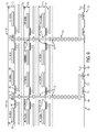
- FIG 2 portions of an embodiment of the image sensor 20 are conceptually illustrated.
- the image sensor 20 is a Complementary Metal Oxide Semiconductor (CMOS) image sensor that includes a first sensor layer 101 having a first array of pixels 111.
- a second sensor layer 102 is situated over the first sensor layer 101, which has a second array of pixels 112.
- a circuit layer 120 is situated below the first sensor layer 101, with support circuitry 122 for the pixel arrays 111,112 of the first and second sensor layers 101,102.
- Interlayer connectors 130 between the pixels 111,112 of the first and second layers 101,102 and the support circuitry 122 provide electrical connections between the respective layers.
- the first sensor layer 101 has a thickness T1 to collect light with a first preselected range of wavelengths and the second sensor layer has a thickness T2 to collect light with a second preselected range of wavelengths.
- Regular silicon wafers, silicon on insulator (SOI) wafers or silicon on sapphire (SOS) wafers are all suitable materials for manufacture of the sensor layers 101, 102.
- FIG. 3 is a block diagram conceptually portions of a pixel 110 of the pixel arrays 111, 112.
- the pixel 110 includes a photodetector, such as a photodiode 140 and a transfer mechanism, such as a transfer gate 142.
- the photodetector 140 collects charge in response to incident light and the transfer gate 142 functions to transfer charge from the photodetector 140 to a charge-to-voltage mechanism, such as a floating diffusion sense node 144, which receives the charge from the photodetector 140 and converts the charge to a voltage signal.
- the pixels 110 are typically configured in arrays of rows and columns.
- a row select transistor is coupled to a column bus, and the readout of charge from the pixels 110 is accomplished by selecting the desired row of the array by activating the proper row select transistor, and the information is read out from the columns of the selected row.
- the pixels 110 of the first and second pixel arrays 111,112 are organized into pixel kernels 150.
- Figures 4A and 4B illustrate examples of some pixel kernel configurations.
- four photodiodes 140 share a common floating diffusion 144 via respective transfer gates 142
- two photodiodes 140 share a common floating diffusion 144.
- the interlayer connectors 130 are coupled to the floating diffusions 144 of the pixel kernels 150.
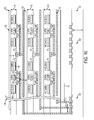
- Figure 5 is a cross-section view showing further aspects of an embodiment of an image sensor having two sensor layers 101,102 and a circuit layer 120.
- Each of the sensor layers 101, 102 and the circuit layer 120 include a silicon portion 152 and one or more metal layers 154.
- the support circuitry 122 of the circuit layer 120 includes a floating diffusion 144 corresponding to each pixel kernel 150, and coupled to the corresponding pixel kernel by the interlayer connectors 130.
- the structure illustrated in Figure 5 has an extra metal layer 154 (the metal layer corresponding to the transfer gate 142) and the wafer interconnection 130 is done through the floating diffusions 144. This allows binning the pixels onto the same floating diffusion 144.
- the support circuitry 122 also includes a reset gate 124, a voltage supply VDD, and a source follower input and output 126, 128 for each pixel kernel 150.
- the interlayer connectors 130 electrically connect the respective floating diffusions nodes 144 on sensing layer T2, sensing layer T1, and the circuit wafer to form a collective floating diffusion 144.
- antireflection coatings are used on both sides of each of the sensing layers and on top on the circuit layer in some embodiments.
- Such antireflection coatings are known, and are used, for example, for single layer structures such as ONO stacks (silicon oxide- silicon nitride - silicon oxide) or hafnium oxide-magnesium oxide stacks.
- ONO stacks silicon oxide- silicon nitride - silicon oxide
- hafnium oxide-magnesium oxide stacks hafnium oxide-magnesium oxide stacks.
- Other suitable antireflection coatings could also be used. These antireflection coatings can be deposited using any typical deposition technique before the sensing and the circuit layer are bonded together.
- Figure 6 illustrates another embodiment where the interlayer connections 130 are implemented by row and column interconnects, which connect the pixels 111 to the circuit layer 120 via row and column circuitry 132.
- An extra two metal layers 154 are included and the wafer interconnections 130 are done through row and column interconnects placed at the periphery of the imager area.
- each output signal and timing line on the sensor layers are electrically coupled with the interconnects 130 to the column or row circuitry 132 on the circuit layer 120.
- standard CMOS digital and analog circuitry is situated outside the image area on sensor layers 101, 102 and/or the circuit wafer 120.
- a color filter array (CFA) 160 is situated over the top sensor layer 102.
- the silicon portions 152 or the first and second sensor layers 101,102 have different thicknesses T1,T2 so that each layer collects light with in a predetermined range of wavelengths.
- the thickness of the sensor layers can be about 0.5 ⁇ m to collect predominantly blue light, about 1.3 ⁇ m to collect predominantly green light, and/or about 3.0 ⁇ m to collect predominantly red light.
- Figures 5 and 6 having two sensor layers 101, 102 with layer thicknesses T1, T2 eliminates the need for two of the layers of the CFA 160.
- Figures 7 and 8 illustrate examples of two complementary CFAs 160, where Y stands for yellow, M stands for magenta and P stands for panchromatic.
- the silicon thickness T2 of the top sensor layer 102 is about 2 ⁇ m in the illustrated embodiments.
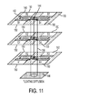
- the embodiments illustrated in Figures 9 and 10 each include an additional sensor layer 103.
- the interlayer connections 130 connect the floating diffusions 144, and in Figure 10 , the interlayer connections 130 are made using the row and column circuitry 132.
- the silicon thickness T3 of the third sensor layer is about 0.5 ⁇ m so that it collects predominantly blue light
- the silicon thickness T2 of the second sensor layer 102 is about 1.3 ⁇ m so that it collects predominantly green light
- the silicon thickness T1 of the first sensor layer is about 3 ⁇ m so that it collects predominantly red light.
- Such a sensor does not require wavelength selective filters to detect color, which are known to decrease quantum efficiency.
- This structure also allows multiple ways of binning pixels onto a common floating diffusion.
- three or more photodiodes 140 can be connected to the same electrical interconnect 130.
- This allows multiple ways of binning the pixels 110.
- the transfer gates 142 for photodiodes B1, G1, and R1 can be activated to transfer charge onto the common floating diffusion 142 and produce a binned panchromatic signal.
- transfer gates 142 for each photodiode 110 in the pixel kernel 150 can be activated to bin all of the color signals and produce a higher sensitivity output at lower spatial resolution.
- red pixels R1+R2+R3+R4 functions like a single large (high sensitivity) red pixel.
- the option also exists to sacrifice spatial resolution for color response in one color plane, but not others.
- the four red pixels could be binned together, but individual photodiode data preserved in the green channel.
- Another option would be to bin all photodiodes (for example using all 12 photodiodes in Figure 11 (four blue pixels B1-B4, four green pixels G1-G4, and four red pixels R1-R4) onto the shared floating diffusion 144. This would produce a high sensitivity, low spatial resolution panchromatic signal for the stacked kernel. Color separation in this case would be accomplished by preserving color separation in nearby kernels.
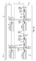
- Figure 12 illustrates another embodiment that includes two sensor layers 101,102 and a circuit layer 120 that also contains sensing elements.
- This structure requires one less wafer as compared to the embodiments illustrated in Figures 9 and 10 while still providing three sensor layers.
- the circuit layer 120 includes pixels 110 in addition to support circuitry.
- the silicon thickness T1,T2,T3 circuit layer 120 and the two sensor layers 101,102 are such that each layer collects light with predetermined ranges of wavelengths.
- the interlayer connections 130 are made through the row and column circuitry 132, though in similar embodiments the connections are made through the floating diffusions 144.
- Figure 13 illustrates an example not forming part of the claimed invention having one sensor layer 101 and a circuit layer 120 that also includes sensing elements.
- the embodiment illustrated in Figure 113 has interlayer connections 130 through the floating diffusions 144, though the connections can alternatively be made through the row and column circuitry as disclosed in other embodiments herein.
- the sensor layer 101 and the circuit layer 120 each have silicon thicknesses T1,T2 to layer collect light with predetermined ranges of wavelengths.
- a complementary CFA 160 such as illustrated in Figures 7 and 8 is provided for filtering the third color.
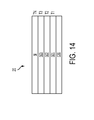
- Figure 14 conceptually illustrates another embodiment having more than three sensing layers 101-N, with each layer having a predetermined thickness for collecting light having corresponding ranges of wavelengths. This structure allows the extension of sensitivity beyond the visible spectrum.
- the top three layers will be responsible for capturing the light in the visible frequency range as described, for example, in the embodiments illustrated in Figures 9 and 10 , while the extra layers N may be used to capture infrared light.
Landscapes
- Engineering & Computer Science (AREA)
- Multimedia (AREA)
- Signal Processing (AREA)
- Solid State Image Pick-Up Elements (AREA)
- Transforming Light Signals Into Electric Signals (AREA)
Applications Claiming Priority (2)
| Application Number | Priority Date | Filing Date | Title |
|---|---|---|---|
| US12/184,314 US8471939B2 (en) | 2008-08-01 | 2008-08-01 | Image sensor having multiple sensing layers |
| PCT/US2009/004051 WO2010014138A1 (en) | 2008-08-01 | 2009-07-13 | Image sensor having multiple sensing layers |
Publications (2)
| Publication Number | Publication Date |
|---|---|
| EP2313927A1 EP2313927A1 (en) | 2011-04-27 |
| EP2313927B1 true EP2313927B1 (en) | 2015-12-02 |
Family
ID=41170970
Family Applications (1)
| Application Number | Title | Priority Date | Filing Date |
|---|---|---|---|
| EP09788904.2A Active EP2313927B1 (en) | 2008-08-01 | 2009-07-13 | Image sensor having multiple sensing layers |
Country Status (7)
| Country | Link |
|---|---|
| US (1) | US8471939B2 (enExample) |
| EP (1) | EP2313927B1 (enExample) |
| JP (1) | JP5562953B2 (enExample) |
| KR (1) | KR101417232B1 (enExample) |
| CN (1) | CN102089882B (enExample) |
| TW (1) | TWI431766B (enExample) |
| WO (1) | WO2010014138A1 (enExample) |
Cited By (1)
| Publication number | Priority date | Publication date | Assignee | Title |
|---|---|---|---|---|
| US11463634B2 (en) | 2020-04-07 | 2022-10-04 | Caeleste Cvba | Charge domain binning in a MOS pixel |
Families Citing this family (54)
| Publication number | Priority date | Publication date | Assignee | Title |
|---|---|---|---|---|
| US20100301437A1 (en) * | 2009-06-01 | 2010-12-02 | Kla-Tencor Corporation | Anti-Reflective Coating For Sensors Suitable For High Throughput Inspection Systems |
| JP5146499B2 (ja) * | 2009-08-08 | 2013-02-20 | 株式会社ニコン | 固体撮像素子 |
| US20110156197A1 (en) * | 2009-12-31 | 2011-06-30 | Tivarus Cristian A | Interwafer interconnects for stacked CMOS image sensors |
| CN102792677B (zh) * | 2010-03-08 | 2015-08-05 | 株式会社半导体能源研究所 | 半导体器件及其制造方法 |
| CA2787911C (en) * | 2010-06-01 | 2017-07-11 | Boly Media Communications (Shenzhen) Co., Ltd. | Multi-spectrum photosensitive devices and methods for sampling the same |
| JP2012015274A (ja) | 2010-06-30 | 2012-01-19 | Canon Inc | 固体撮像装置、及び固体撮像装置の製造方法。 |
| FR2966978B1 (fr) * | 2010-11-03 | 2016-04-01 | Commissariat Energie Atomique | Detecteur de rayonnement visible et proche infrarouge |
| FR2966977B1 (fr) * | 2010-11-03 | 2016-02-26 | Commissariat Energie Atomique | Detecteur de rayonnement visible et proche infrarouge |
| CN102256047B (zh) * | 2011-07-28 | 2013-06-19 | 北京空间机电研究所 | 一种基于滤波的2×2数字binning系统 |
| KR101399338B1 (ko) * | 2011-08-08 | 2014-05-30 | (주)실리콘화일 | 이중 감지 기능을 가지는 기판 적층형 이미지 센서 |
| JP5999750B2 (ja) * | 2011-08-25 | 2016-09-28 | ソニー株式会社 | 撮像素子、撮像装置及び生体撮像装置 |
| JP2013070030A (ja) * | 2011-09-06 | 2013-04-18 | Sony Corp | 撮像素子、電子機器、並びに、情報処理装置 |
| JP2013187475A (ja) * | 2012-03-09 | 2013-09-19 | Olympus Corp | 固体撮像装置およびカメラシステム |
| US8686342B2 (en) * | 2012-04-09 | 2014-04-01 | Omnivision Technologies, Inc. | Double-sided image sensor formed on a single semiconductor wafer die |
| JP6042636B2 (ja) * | 2012-05-28 | 2016-12-14 | オリンパス株式会社 | 固体撮像素子および固体撮像装置 |
| JP2014022561A (ja) | 2012-07-18 | 2014-02-03 | Sony Corp | 固体撮像装置、及び、電子機器 |
| JP6128787B2 (ja) | 2012-09-28 | 2017-05-17 | キヤノン株式会社 | 半導体装置 |
| JP2014099582A (ja) * | 2012-10-18 | 2014-05-29 | Sony Corp | 固体撮像装置 |
| JP2014199898A (ja) * | 2013-03-11 | 2014-10-23 | ソニー株式会社 | 固体撮像素子および製造方法、並びに、電子機器 |
| JP6136669B2 (ja) * | 2013-07-08 | 2017-05-31 | 株式会社ニコン | 撮像装置 |
| KR102065633B1 (ko) | 2013-08-12 | 2020-01-13 | 삼성전자 주식회사 | 이미지 센서, 이의 동작 방법, 및 이를 포함하는 시스템 |
| CN105975126A (zh) * | 2013-09-29 | 2016-09-28 | 宸鸿科技(厦门)有限公司 | 触控面板及其制作方法 |
| JP6177117B2 (ja) * | 2013-12-10 | 2017-08-09 | オリンパス株式会社 | 固体撮像装置、撮像装置、固体撮像装置の製造方法 |
| US9347890B2 (en) | 2013-12-19 | 2016-05-24 | Kla-Tencor Corporation | Low-noise sensor and an inspection system using a low-noise sensor |
| US9748294B2 (en) | 2014-01-10 | 2017-08-29 | Hamamatsu Photonics K.K. | Anti-reflection layer for back-illuminated sensor |
| JP2015162604A (ja) * | 2014-02-27 | 2015-09-07 | 株式会社東芝 | Cmosイメージセンサ |
| US9410901B2 (en) | 2014-03-17 | 2016-08-09 | Kla-Tencor Corporation | Image sensor, an inspection system and a method of inspecting an article |
| JP2015192015A (ja) * | 2014-03-28 | 2015-11-02 | オリンパス株式会社 | 固体撮像装置 |
| US9438866B2 (en) | 2014-04-23 | 2016-09-06 | Omnivision Technologies, Inc. | Image sensor with scaled filter array and in-pixel binning |
| US10211250B2 (en) * | 2014-07-03 | 2019-02-19 | Sony Semiconductor Solutions Corporation | Solid-state image sensor electronic device |
| JP6218687B2 (ja) * | 2014-07-17 | 2017-10-25 | オリンパス株式会社 | 固体撮像装置および撮像装置 |
| WO2016103315A1 (ja) * | 2014-12-22 | 2016-06-30 | オリンパス株式会社 | 固体撮像装置および撮像装置 |
| JP6388669B2 (ja) * | 2015-01-09 | 2018-09-12 | オリンパス株式会社 | 固体撮像装置 |
| US10163968B2 (en) * | 2015-01-23 | 2018-12-25 | Dartmouth College | Multi-junction pixel image sensor with dielectric reflector between photodetection layers |
| US9860466B2 (en) | 2015-05-14 | 2018-01-02 | Kla-Tencor Corporation | Sensor with electrically controllable aperture for inspection and metrology systems |
| US9686486B2 (en) * | 2015-05-27 | 2017-06-20 | Semiconductor Components Industries, Llc | Multi-resolution pixel architecture with shared floating diffusion nodes |
| US10341592B2 (en) | 2015-06-09 | 2019-07-02 | Sony Semiconductor Solutions Corporation | Imaging element, driving method, and electronic device |
| JP6607262B2 (ja) * | 2016-01-08 | 2019-11-20 | 株式会社ニコン | 撮像素子および撮像装置 |
| US10778925B2 (en) | 2016-04-06 | 2020-09-15 | Kla-Tencor Corporation | Multiple column per channel CCD sensor architecture for inspection and metrology |
| US10313622B2 (en) | 2016-04-06 | 2019-06-04 | Kla-Tencor Corporation | Dual-column-parallel CCD sensor and inspection systems using a sensor |
| US10313609B2 (en) * | 2016-04-14 | 2019-06-04 | Qualcomm Incorporated | Image sensors having pixel-binning with configurable shared floating diffusion |
| KR102524400B1 (ko) * | 2016-07-04 | 2023-04-24 | 에스케이하이닉스 주식회사 | 하나의 컬러 필터 및 하나의 마이크로렌즈를 공유하는 다수 개의 포토다이오드들을 갖는 이미지 센서 |
| KR102549621B1 (ko) * | 2016-09-02 | 2023-06-28 | 삼성전자주식회사 | 반도체 장치 |
| US9818791B1 (en) * | 2016-10-04 | 2017-11-14 | Omnivision Technologies, Inc. | Stacked image sensor |
| JP2018081946A (ja) | 2016-11-14 | 2018-05-24 | ソニーセミコンダクタソリューションズ株式会社 | 固体撮像装置およびその製造方法、並びに電子機器 |
| JP7038494B2 (ja) * | 2017-06-15 | 2022-03-18 | ルネサスエレクトロニクス株式会社 | 固体撮像素子 |
| US10468448B2 (en) * | 2017-11-30 | 2019-11-05 | Taiwan Semiconductor Manufacturing Company Ltd. | Semiconductor image sensor and method for forming the same |
| JP7262011B2 (ja) * | 2018-11-19 | 2023-04-21 | パナソニックIpマネジメント株式会社 | 撮像装置及び撮像システム |
| US11114491B2 (en) | 2018-12-12 | 2021-09-07 | Kla Corporation | Back-illuminated sensor and a method of manufacturing a sensor |
| US20240038814A1 (en) * | 2020-12-28 | 2024-02-01 | Sony Semiconductor Solutions Corporation | Solid-state imaging device, method of manufacturing the same, and electronic device |
| US12205973B2 (en) | 2021-01-14 | 2025-01-21 | Imec Vzw | Image sensor comprising stacked photo-sensitive devices |
| JPWO2023171008A1 (enExample) * | 2022-03-09 | 2023-09-14 | ||
| WO2024202539A1 (ja) * | 2023-03-31 | 2024-10-03 | ソニーセミコンダクタソリューションズ株式会社 | 光検出装置 |
| WO2025047330A1 (ja) * | 2023-08-31 | 2025-03-06 | パナソニックIpマネジメント株式会社 | 撮像装置 |
Family Cites Families (37)
| Publication number | Priority date | Publication date | Assignee | Title |
|---|---|---|---|---|
| US4438455A (en) * | 1981-12-15 | 1984-03-20 | Fuji Photo Film Co., Ltd. | Solid-state color imager with three layer four story structure |
| US4677289A (en) * | 1984-11-12 | 1987-06-30 | Kabushiki Kaisha Toshiba | Color sensor |
| JPH01151262A (ja) * | 1987-12-09 | 1989-06-14 | Fuji Photo Film Co Ltd | 計測用イメージセンサー |
| JP2617798B2 (ja) | 1989-09-22 | 1997-06-04 | 三菱電機株式会社 | 積層型半導体装置およびその製造方法 |
| JPH10284714A (ja) | 1997-04-07 | 1998-10-23 | Toshiba Corp | 固体撮像装置及びこれを用いた撮像システム |
| DE19737561C1 (de) * | 1997-08-28 | 1999-04-15 | Forschungszentrum Juelich Gmbh | Mehrfarbensensor |
| US6693670B1 (en) * | 1999-07-29 | 2004-02-17 | Vision - Sciences, Inc. | Multi-photodetector unit cell |
| JP3713418B2 (ja) | 2000-05-30 | 2005-11-09 | 光正 小柳 | 3次元画像処理装置の製造方法 |
| JP4031901B2 (ja) | 2000-07-19 | 2008-01-09 | 株式会社東芝 | 固体撮像装置 |
| KR20050043754A (ko) * | 2001-11-05 | 2005-05-11 | 미츠마사 코야나기 | 고체 영상센서 및 그 제조방법 |
| JP2003298038A (ja) * | 2002-04-05 | 2003-10-17 | Canon Inc | 光電変換素子及びそれを用いた固体撮像装置 |
| US6933489B2 (en) | 2002-05-10 | 2005-08-23 | Hamamatsu Photonics K.K. | Back illuminated photodiode array and method of manufacturing the same |
| US6646318B1 (en) * | 2002-08-15 | 2003-11-11 | National Semiconductor Corporation | Bandgap tuned vertical color imager cell |
| US7154157B2 (en) * | 2002-12-30 | 2006-12-26 | Intel Corporation | Stacked semiconductor radiation sensors having color component and infrared sensing capability |
| US7339216B1 (en) * | 2003-01-31 | 2008-03-04 | Foveon, Inc. | Vertical color filter sensor group array with full-resolution top layer and lower-resolution lower layer |
| JP4075678B2 (ja) * | 2003-05-06 | 2008-04-16 | ソニー株式会社 | 固体撮像素子 |
| CN100407433C (zh) | 2003-05-23 | 2008-07-30 | 浜松光子学株式会社 | 光检测装置 |
| US7214999B2 (en) | 2003-10-31 | 2007-05-08 | Motorola, Inc. | Integrated photoserver for CMOS imagers |
| JP4046067B2 (ja) | 2003-11-04 | 2008-02-13 | ソニー株式会社 | 固体撮像素子の製造方法 |
| US20050109917A1 (en) * | 2003-11-26 | 2005-05-26 | Wong Hon-Sum P. | Multi-spectral imaging with almost-full fill-factor using 3D pixels |
| JP4186851B2 (ja) | 2004-03-18 | 2008-11-26 | ヤマハ株式会社 | 演奏情報表示装置およびプログラム |
| JP2005268479A (ja) | 2004-03-18 | 2005-09-29 | Fuji Film Microdevices Co Ltd | 光電変換膜積層型固体撮像装置 |
| JP4491323B2 (ja) * | 2004-10-22 | 2010-06-30 | 富士フイルム株式会社 | 光電変換膜積層型カラー固体撮像装置 |
| KR100598015B1 (ko) * | 2005-02-07 | 2006-07-06 | 삼성전자주식회사 | 공유 구조 상보성 금속 산화막 반도체 액티브 픽셀 센서어레이의 레이 아웃 |
| US7271025B2 (en) * | 2005-07-12 | 2007-09-18 | Micron Technology, Inc. | Image sensor with SOI substrate |
| FR2888989B1 (fr) | 2005-07-21 | 2008-06-06 | St Microelectronics Sa | Capteur d'images |
| JP4984634B2 (ja) * | 2005-07-21 | 2012-07-25 | ソニー株式会社 | 物理情報取得方法および物理情報取得装置 |
| US8139130B2 (en) | 2005-07-28 | 2012-03-20 | Omnivision Technologies, Inc. | Image sensor with improved light sensitivity |
| JP2007059517A (ja) * | 2005-08-23 | 2007-03-08 | Fujifilm Corp | 光電変換膜、光電変換素子、及び撮像素子、並びに、これらに電場を印加する方法 |
| KR100775058B1 (ko) * | 2005-09-29 | 2007-11-08 | 삼성전자주식회사 | 픽셀 및 이를 이용한 이미지 센서, 그리고 상기 이미지센서를 포함하는 이미지 처리 시스템 |
| JP2007228460A (ja) | 2006-02-27 | 2007-09-06 | Mitsumasa Koyanagi | 集積センサを搭載した積層型半導体装置 |
| US7419844B2 (en) * | 2006-03-17 | 2008-09-02 | Sharp Laboratories Of America, Inc. | Real-time CMOS imager having stacked photodiodes fabricated on SOI wafer |
| JP4130211B2 (ja) | 2006-05-31 | 2008-08-06 | 三洋電機株式会社 | 撮像装置 |
| US8049256B2 (en) | 2006-10-05 | 2011-11-01 | Omnivision Technologies, Inc. | Active pixel sensor having a sensor wafer connected to a support circuit wafer |
| KR100825808B1 (ko) * | 2007-02-26 | 2008-04-29 | 삼성전자주식회사 | 후면 조명 구조의 이미지 센서 및 그 이미지 센서 제조방법 |
| US8106426B2 (en) * | 2008-02-04 | 2012-01-31 | Sharp Laboratories Of America, Inc. | Full color CMOS imager filter |
| US7893468B2 (en) * | 2008-05-30 | 2011-02-22 | International Business Machines Corporation | Optical sensor including stacked photodiodes |
-
2008
- 2008-08-01 US US12/184,314 patent/US8471939B2/en active Active
-
2009
- 2009-07-13 EP EP09788904.2A patent/EP2313927B1/en active Active
- 2009-07-13 WO PCT/US2009/004051 patent/WO2010014138A1/en not_active Ceased
- 2009-07-13 KR KR1020117002504A patent/KR101417232B1/ko active Active
- 2009-07-13 CN CN200980127273XA patent/CN102089882B/zh active Active
- 2009-07-13 JP JP2011521091A patent/JP5562953B2/ja active Active
- 2009-07-31 TW TW098125958A patent/TWI431766B/zh active
Cited By (1)
| Publication number | Priority date | Publication date | Assignee | Title |
|---|---|---|---|---|
| US11463634B2 (en) | 2020-04-07 | 2022-10-04 | Caeleste Cvba | Charge domain binning in a MOS pixel |
Also Published As
| Publication number | Publication date |
|---|---|
| KR20110036823A (ko) | 2011-04-11 |
| TW201013910A (en) | 2010-04-01 |
| JP5562953B2 (ja) | 2014-07-30 |
| KR101417232B1 (ko) | 2014-07-08 |
| CN102089882B (zh) | 2013-07-24 |
| EP2313927A1 (en) | 2011-04-27 |
| CN102089882A (zh) | 2011-06-08 |
| US8471939B2 (en) | 2013-06-25 |
| TWI431766B (zh) | 2014-03-21 |
| WO2010014138A1 (en) | 2010-02-04 |
| US20100026865A1 (en) | 2010-02-04 |
| JP2011530165A (ja) | 2011-12-15 |
Similar Documents
| Publication | Publication Date | Title |
|---|---|---|
| EP2313927B1 (en) | Image sensor having multiple sensing layers | |
| US7781716B2 (en) | Stacked image sensor with shared diffusion regions in respective dropped pixel positions of a pixel array | |
| CN102177585B (zh) | 具有多个感测层的图像传感器及其操作与制作方法 | |
| US9319611B2 (en) | Image sensor with flexible pixel summing | |
| KR102398120B1 (ko) | 고체 촬상 소자 및 그 제조 방법, 및 전자 기기 | |
| US20100149396A1 (en) | Image sensor with inlaid color pixels in etched panchromatic array | |
| US8947572B2 (en) | Dual-sided image sensor | |
| CN207896093U (zh) | 图像传感器和成像系统 | |
| US20110157395A1 (en) | Image sensor with fractional resolution image processing | |
| CN207731929U (zh) | 图像传感器以及成像系统 | |
| US20100149379A1 (en) | Image sensor with three-dimensional interconnect and ccd |
Legal Events
| Date | Code | Title | Description |
|---|---|---|---|
| PUAI | Public reference made under article 153(3) epc to a published international application that has entered the european phase |
Free format text: ORIGINAL CODE: 0009012 |
|
| 17P | Request for examination filed |
Effective date: 20110128 |
|
| AK | Designated contracting states |
Kind code of ref document: A1 Designated state(s): AT BE BG CH CY CZ DE DK EE ES FI FR GB GR HR HU IE IS IT LI LT LU LV MC MK MT NL NO PL PT RO SE SI SK SM TR |
|
| AX | Request for extension of the european patent |
Extension state: AL BA RS |
|
| RAP1 | Party data changed (applicant data changed or rights of an application transferred) |
Owner name: OMNIVISION TECHNOLOGIES, INC. |
|
| DAX | Request for extension of the european patent (deleted) | ||
| 17Q | First examination report despatched |
Effective date: 20141126 |
|
| GRAP | Despatch of communication of intention to grant a patent |
Free format text: ORIGINAL CODE: EPIDOSNIGR1 |
|
| INTG | Intention to grant announced |
Effective date: 20150720 |
|
| GRAS | Grant fee paid |
Free format text: ORIGINAL CODE: EPIDOSNIGR3 |
|
| GRAA | (expected) grant |
Free format text: ORIGINAL CODE: 0009210 |
|
| AK | Designated contracting states |
Kind code of ref document: B1 Designated state(s): AT BE BG CH CY CZ DE DK EE ES FI FR GB GR HR HU IE IS IT LI LT LU LV MC MK MT NL NO PL PT RO SE SI SK SM TR |
|
| REG | Reference to a national code |
Ref country code: GB Ref legal event code: FG4D |
|
| REG | Reference to a national code |
Ref country code: AT Ref legal event code: REF Ref document number: 763966 Country of ref document: AT Kind code of ref document: T Effective date: 20151215 Ref country code: CH Ref legal event code: EP |
|
| REG | Reference to a national code |
Ref country code: IE Ref legal event code: FG4D |
|
| REG | Reference to a national code |
Ref country code: DE Ref legal event code: R096 Ref document number: 602009035128 Country of ref document: DE |
|
| REG | Reference to a national code |
Ref country code: NL Ref legal event code: MP Effective date: 20160302 |
|
| REG | Reference to a national code |
Ref country code: LT Ref legal event code: MG4D |
|
| REG | Reference to a national code |
Ref country code: AT Ref legal event code: MK05 Ref document number: 763966 Country of ref document: AT Kind code of ref document: T Effective date: 20151202 |
|
| PG25 | Lapsed in a contracting state [announced via postgrant information from national office to epo] |
Ref country code: NO Free format text: LAPSE BECAUSE OF FAILURE TO SUBMIT A TRANSLATION OF THE DESCRIPTION OR TO PAY THE FEE WITHIN THE PRESCRIBED TIME-LIMIT Effective date: 20160302 Ref country code: ES Free format text: LAPSE BECAUSE OF FAILURE TO SUBMIT A TRANSLATION OF THE DESCRIPTION OR TO PAY THE FEE WITHIN THE PRESCRIBED TIME-LIMIT Effective date: 20151202 Ref country code: HR Free format text: LAPSE BECAUSE OF FAILURE TO SUBMIT A TRANSLATION OF THE DESCRIPTION OR TO PAY THE FEE WITHIN THE PRESCRIBED TIME-LIMIT Effective date: 20151202 Ref country code: LT Free format text: LAPSE BECAUSE OF FAILURE TO SUBMIT A TRANSLATION OF THE DESCRIPTION OR TO PAY THE FEE WITHIN THE PRESCRIBED TIME-LIMIT Effective date: 20151202 |
|
| REG | Reference to a national code |
Ref country code: FR Ref legal event code: PLFP Year of fee payment: 8 |
|
| PG25 | Lapsed in a contracting state [announced via postgrant information from national office to epo] |
Ref country code: GR Free format text: LAPSE BECAUSE OF FAILURE TO SUBMIT A TRANSLATION OF THE DESCRIPTION OR TO PAY THE FEE WITHIN THE PRESCRIBED TIME-LIMIT Effective date: 20160303 Ref country code: SE Free format text: LAPSE BECAUSE OF FAILURE TO SUBMIT A TRANSLATION OF THE DESCRIPTION OR TO PAY THE FEE WITHIN THE PRESCRIBED TIME-LIMIT Effective date: 20151202 Ref country code: PL Free format text: LAPSE BECAUSE OF FAILURE TO SUBMIT A TRANSLATION OF THE DESCRIPTION OR TO PAY THE FEE WITHIN THE PRESCRIBED TIME-LIMIT Effective date: 20151202 Ref country code: AT Free format text: LAPSE BECAUSE OF FAILURE TO SUBMIT A TRANSLATION OF THE DESCRIPTION OR TO PAY THE FEE WITHIN THE PRESCRIBED TIME-LIMIT Effective date: 20151202 Ref country code: LV Free format text: LAPSE BECAUSE OF FAILURE TO SUBMIT A TRANSLATION OF THE DESCRIPTION OR TO PAY THE FEE WITHIN THE PRESCRIBED TIME-LIMIT Effective date: 20151202 Ref country code: NL Free format text: LAPSE BECAUSE OF FAILURE TO SUBMIT A TRANSLATION OF THE DESCRIPTION OR TO PAY THE FEE WITHIN THE PRESCRIBED TIME-LIMIT Effective date: 20151202 Ref country code: FI Free format text: LAPSE BECAUSE OF FAILURE TO SUBMIT A TRANSLATION OF THE DESCRIPTION OR TO PAY THE FEE WITHIN THE PRESCRIBED TIME-LIMIT Effective date: 20151202 |
|
| PG25 | Lapsed in a contracting state [announced via postgrant information from national office to epo] |
Ref country code: IS Free format text: LAPSE BECAUSE OF FAILURE TO SUBMIT A TRANSLATION OF THE DESCRIPTION OR TO PAY THE FEE WITHIN THE PRESCRIBED TIME-LIMIT Effective date: 20151202 |
|
| PG25 | Lapsed in a contracting state [announced via postgrant information from national office to epo] |
Ref country code: CZ Free format text: LAPSE BECAUSE OF FAILURE TO SUBMIT A TRANSLATION OF THE DESCRIPTION OR TO PAY THE FEE WITHIN THE PRESCRIBED TIME-LIMIT Effective date: 20151202 Ref country code: IT Free format text: LAPSE BECAUSE OF FAILURE TO SUBMIT A TRANSLATION OF THE DESCRIPTION OR TO PAY THE FEE WITHIN THE PRESCRIBED TIME-LIMIT Effective date: 20151202 |
|
| PG25 | Lapsed in a contracting state [announced via postgrant information from national office to epo] |
Ref country code: SM Free format text: LAPSE BECAUSE OF FAILURE TO SUBMIT A TRANSLATION OF THE DESCRIPTION OR TO PAY THE FEE WITHIN THE PRESCRIBED TIME-LIMIT Effective date: 20151202 Ref country code: EE Free format text: LAPSE BECAUSE OF FAILURE TO SUBMIT A TRANSLATION OF THE DESCRIPTION OR TO PAY THE FEE WITHIN THE PRESCRIBED TIME-LIMIT Effective date: 20151202 Ref country code: RO Free format text: LAPSE BECAUSE OF FAILURE TO SUBMIT A TRANSLATION OF THE DESCRIPTION OR TO PAY THE FEE WITHIN THE PRESCRIBED TIME-LIMIT Effective date: 20151202 Ref country code: PT Free format text: LAPSE BECAUSE OF FAILURE TO SUBMIT A TRANSLATION OF THE DESCRIPTION OR TO PAY THE FEE WITHIN THE PRESCRIBED TIME-LIMIT Effective date: 20160404 Ref country code: SK Free format text: LAPSE BECAUSE OF FAILURE TO SUBMIT A TRANSLATION OF THE DESCRIPTION OR TO PAY THE FEE WITHIN THE PRESCRIBED TIME-LIMIT Effective date: 20151202 Ref country code: IS Free format text: LAPSE BECAUSE OF FAILURE TO SUBMIT A TRANSLATION OF THE DESCRIPTION OR TO PAY THE FEE WITHIN THE PRESCRIBED TIME-LIMIT Effective date: 20160402 |
|
| REG | Reference to a national code |
Ref country code: DE Ref legal event code: R097 Ref document number: 602009035128 Country of ref document: DE |
|
| PLBE | No opposition filed within time limit |
Free format text: ORIGINAL CODE: 0009261 |
|
| STAA | Information on the status of an ep patent application or granted ep patent |
Free format text: STATUS: NO OPPOSITION FILED WITHIN TIME LIMIT |
|
| PG25 | Lapsed in a contracting state [announced via postgrant information from national office to epo] |
Ref country code: DK Free format text: LAPSE BECAUSE OF FAILURE TO SUBMIT A TRANSLATION OF THE DESCRIPTION OR TO PAY THE FEE WITHIN THE PRESCRIBED TIME-LIMIT Effective date: 20151202 |
|
| 26N | No opposition filed |
Effective date: 20160905 |
|
| PG25 | Lapsed in a contracting state [announced via postgrant information from national office to epo] |
Ref country code: SI Free format text: LAPSE BECAUSE OF FAILURE TO SUBMIT A TRANSLATION OF THE DESCRIPTION OR TO PAY THE FEE WITHIN THE PRESCRIBED TIME-LIMIT Effective date: 20151202 |
|
| PG25 | Lapsed in a contracting state [announced via postgrant information from national office to epo] |
Ref country code: BE Free format text: LAPSE BECAUSE OF FAILURE TO SUBMIT A TRANSLATION OF THE DESCRIPTION OR TO PAY THE FEE WITHIN THE PRESCRIBED TIME-LIMIT Effective date: 20151202 |
|
| PG25 | Lapsed in a contracting state [announced via postgrant information from national office to epo] |
Ref country code: MC Free format text: LAPSE BECAUSE OF FAILURE TO SUBMIT A TRANSLATION OF THE DESCRIPTION OR TO PAY THE FEE WITHIN THE PRESCRIBED TIME-LIMIT Effective date: 20151202 |
|
| REG | Reference to a national code |
Ref country code: IE Ref legal event code: MM4A |
|
| REG | Reference to a national code |
Ref country code: FR Ref legal event code: PLFP Year of fee payment: 9 |
|
| PG25 | Lapsed in a contracting state [announced via postgrant information from national office to epo] |
Ref country code: IE Free format text: LAPSE BECAUSE OF NON-PAYMENT OF DUE FEES Effective date: 20160713 |
|
| PG25 | Lapsed in a contracting state [announced via postgrant information from national office to epo] |
Ref country code: LU Free format text: LAPSE BECAUSE OF NON-PAYMENT OF DUE FEES Effective date: 20160713 |
|
| PG25 | Lapsed in a contracting state [announced via postgrant information from national office to epo] |
Ref country code: CY Free format text: LAPSE BECAUSE OF FAILURE TO SUBMIT A TRANSLATION OF THE DESCRIPTION OR TO PAY THE FEE WITHIN THE PRESCRIBED TIME-LIMIT Effective date: 20151202 Ref country code: HU Free format text: LAPSE BECAUSE OF FAILURE TO SUBMIT A TRANSLATION OF THE DESCRIPTION OR TO PAY THE FEE WITHIN THE PRESCRIBED TIME-LIMIT; INVALID AB INITIO Effective date: 20090713 |
|
| REG | Reference to a national code |
Ref country code: FR Ref legal event code: PLFP Year of fee payment: 10 |
|
| PG25 | Lapsed in a contracting state [announced via postgrant information from national office to epo] |
Ref country code: MT Free format text: LAPSE BECAUSE OF NON-PAYMENT OF DUE FEES Effective date: 20160731 Ref country code: TR Free format text: LAPSE BECAUSE OF FAILURE TO SUBMIT A TRANSLATION OF THE DESCRIPTION OR TO PAY THE FEE WITHIN THE PRESCRIBED TIME-LIMIT Effective date: 20151202 Ref country code: MK Free format text: LAPSE BECAUSE OF FAILURE TO SUBMIT A TRANSLATION OF THE DESCRIPTION OR TO PAY THE FEE WITHIN THE PRESCRIBED TIME-LIMIT Effective date: 20151202 |
|
| PG25 | Lapsed in a contracting state [announced via postgrant information from national office to epo] |
Ref country code: BG Free format text: LAPSE BECAUSE OF FAILURE TO SUBMIT A TRANSLATION OF THE DESCRIPTION OR TO PAY THE FEE WITHIN THE PRESCRIBED TIME-LIMIT Effective date: 20151202 |
|
| P01 | Opt-out of the competence of the unified patent court (upc) registered |
Effective date: 20230419 |
|
| REG | Reference to a national code |
Ref country code: DE Ref legal event code: R079 Ref document number: 602009035128 Country of ref document: DE Free format text: PREVIOUS MAIN CLASS: H01L0027146000 Ipc: H10F0039180000 |
|
| PGFP | Annual fee paid to national office [announced via postgrant information from national office to epo] |
Ref country code: GB Payment date: 20250612 Year of fee payment: 17 |
|
| PGFP | Annual fee paid to national office [announced via postgrant information from national office to epo] |
Ref country code: FR Payment date: 20250612 Year of fee payment: 17 |
|
| PGFP | Annual fee paid to national office [announced via postgrant information from national office to epo] |
Ref country code: DE Payment date: 20250616 Year of fee payment: 17 |
|
| PGFP | Annual fee paid to national office [announced via postgrant information from national office to epo] |
Ref country code: CH Payment date: 20250801 Year of fee payment: 17 |