EP2297780B1 - Optoelektronisches modul mit einem trägersubstrat und einer mehrzahl von strahlung emittierenden halbleiterbauelementen und verfahren zu dessen herstellung - Google Patents
Optoelektronisches modul mit einem trägersubstrat und einer mehrzahl von strahlung emittierenden halbleiterbauelementen und verfahren zu dessen herstellung Download PDFInfo
- Publication number
- EP2297780B1 EP2297780B1 EP09740632.6A EP09740632A EP2297780B1 EP 2297780 B1 EP2297780 B1 EP 2297780B1 EP 09740632 A EP09740632 A EP 09740632A EP 2297780 B1 EP2297780 B1 EP 2297780B1
- Authority
- EP
- European Patent Office
- Prior art keywords
- radiation
- emitting semiconductor
- semiconductor components
- carrier substrate
- contact surface
- Prior art date
- Legal status (The legal status is an assumption and is not a legal conclusion. Google has not performed a legal analysis and makes no representation as to the accuracy of the status listed.)
- Active
Links
Images

Classifications
-
- H—ELECTRICITY
- H01—ELECTRIC ELEMENTS
- H01L—SEMICONDUCTOR DEVICES NOT COVERED BY CLASS H10
- H01L25/00—Assemblies consisting of a plurality of semiconductor or other solid state devices
- H01L25/03—Assemblies consisting of a plurality of semiconductor or other solid state devices all the devices being of a type provided for in a single subclass of subclasses H10B, H10D, H10F, H10H, H10K or H10N, e.g. assemblies of rectifier diodes
- H01L25/04—Assemblies consisting of a plurality of semiconductor or other solid state devices all the devices being of a type provided for in a single subclass of subclasses H10B, H10D, H10F, H10H, H10K or H10N, e.g. assemblies of rectifier diodes the devices not having separate containers
- H01L25/075—Assemblies consisting of a plurality of semiconductor or other solid state devices all the devices being of a type provided for in a single subclass of subclasses H10B, H10D, H10F, H10H, H10K or H10N, e.g. assemblies of rectifier diodes the devices not having separate containers the devices being of a type provided for in group H10H20/00
-
- H—ELECTRICITY
- H10—SEMICONDUCTOR DEVICES; ELECTRIC SOLID-STATE DEVICES NOT OTHERWISE PROVIDED FOR
- H10H—INORGANIC LIGHT-EMITTING SEMICONDUCTOR DEVICES HAVING POTENTIAL BARRIERS
- H10H20/00—Individual inorganic light-emitting semiconductor devices having potential barriers, e.g. light-emitting diodes [LED]
- H10H20/80—Constructional details
- H10H20/85—Packages
- H10H20/857—Interconnections, e.g. lead-frames, bond wires or solder balls
-
- H—ELECTRICITY
- H01—ELECTRIC ELEMENTS
- H01L—SEMICONDUCTOR DEVICES NOT COVERED BY CLASS H10
- H01L24/00—Arrangements for connecting or disconnecting semiconductor or solid-state bodies; Methods or apparatus related thereto
- H01L24/01—Means for bonding being attached to, or being formed on, the surface to be connected, e.g. chip-to-package, die-attach, "first-level" interconnects; Manufacturing methods related thereto
- H01L24/18—High density interconnect [HDI] connectors; Manufacturing methods related thereto
- H01L24/23—Structure, shape, material or disposition of the high density interconnect connectors after the connecting process
- H01L24/24—Structure, shape, material or disposition of the high density interconnect connectors after the connecting process of an individual high density interconnect connector
-
- H—ELECTRICITY
- H01—ELECTRIC ELEMENTS
- H01L—SEMICONDUCTOR DEVICES NOT COVERED BY CLASS H10
- H01L24/00—Arrangements for connecting or disconnecting semiconductor or solid-state bodies; Methods or apparatus related thereto
- H01L24/80—Methods for connecting semiconductor or other solid state bodies using means for bonding being attached to, or being formed on, the surface to be connected
- H01L24/82—Methods for connecting semiconductor or other solid state bodies using means for bonding being attached to, or being formed on, the surface to be connected by forming build-up interconnects at chip-level, e.g. for high density interconnects [HDI]
-
- H—ELECTRICITY
- H01—ELECTRIC ELEMENTS
- H01L—SEMICONDUCTOR DEVICES NOT COVERED BY CLASS H10
- H01L25/00—Assemblies consisting of a plurality of semiconductor or other solid state devices
- H01L25/03—Assemblies consisting of a plurality of semiconductor or other solid state devices all the devices being of a type provided for in a single subclass of subclasses H10B, H10D, H10F, H10H, H10K or H10N, e.g. assemblies of rectifier diodes
- H01L25/04—Assemblies consisting of a plurality of semiconductor or other solid state devices all the devices being of a type provided for in a single subclass of subclasses H10B, H10D, H10F, H10H, H10K or H10N, e.g. assemblies of rectifier diodes the devices not having separate containers
- H01L25/075—Assemblies consisting of a plurality of semiconductor or other solid state devices all the devices being of a type provided for in a single subclass of subclasses H10B, H10D, H10F, H10H, H10K or H10N, e.g. assemblies of rectifier diodes the devices not having separate containers the devices being of a type provided for in group H10H20/00
- H01L25/0753—Assemblies consisting of a plurality of semiconductor or other solid state devices all the devices being of a type provided for in a single subclass of subclasses H10B, H10D, H10F, H10H, H10K or H10N, e.g. assemblies of rectifier diodes the devices not having separate containers the devices being of a type provided for in group H10H20/00 the devices being arranged next to each other
-
- H—ELECTRICITY
- H10—SEMICONDUCTOR DEVICES; ELECTRIC SOLID-STATE DEVICES NOT OTHERWISE PROVIDED FOR
- H10H—INORGANIC LIGHT-EMITTING SEMICONDUCTOR DEVICES HAVING POTENTIAL BARRIERS
- H10H20/00—Individual inorganic light-emitting semiconductor devices having potential barriers, e.g. light-emitting diodes [LED]
- H10H20/80—Constructional details
-
- H—ELECTRICITY
- H10—SEMICONDUCTOR DEVICES; ELECTRIC SOLID-STATE DEVICES NOT OTHERWISE PROVIDED FOR
- H10H—INORGANIC LIGHT-EMITTING SEMICONDUCTOR DEVICES HAVING POTENTIAL BARRIERS
- H10H29/00—Integrated devices, or assemblies of multiple devices, comprising at least one light-emitting semiconductor element covered by group H10H20/00
- H10H29/10—Integrated devices comprising at least one light-emitting semiconductor component covered by group H10H20/00
-
- H—ELECTRICITY
- H01—ELECTRIC ELEMENTS
- H01L—SEMICONDUCTOR DEVICES NOT COVERED BY CLASS H10
- H01L2224/00—Indexing scheme for arrangements for connecting or disconnecting semiconductor or solid-state bodies and methods related thereto as covered by H01L24/00
- H01L2224/01—Means for bonding being attached to, or being formed on, the surface to be connected, e.g. chip-to-package, die-attach, "first-level" interconnects; Manufacturing methods related thereto
- H01L2224/18—High density interconnect [HDI] connectors; Manufacturing methods related thereto
- H01L2224/23—Structure, shape, material or disposition of the high density interconnect connectors after the connecting process
- H01L2224/24—Structure, shape, material or disposition of the high density interconnect connectors after the connecting process of an individual high density interconnect connector
- H01L2224/241—Disposition
- H01L2224/24105—Connecting bonding areas at different heights
-
- H—ELECTRICITY
- H01—ELECTRIC ELEMENTS
- H01L—SEMICONDUCTOR DEVICES NOT COVERED BY CLASS H10
- H01L2224/00—Indexing scheme for arrangements for connecting or disconnecting semiconductor or solid-state bodies and methods related thereto as covered by H01L24/00
- H01L2224/01—Means for bonding being attached to, or being formed on, the surface to be connected, e.g. chip-to-package, die-attach, "first-level" interconnects; Manufacturing methods related thereto
- H01L2224/18—High density interconnect [HDI] connectors; Manufacturing methods related thereto
- H01L2224/23—Structure, shape, material or disposition of the high density interconnect connectors after the connecting process
- H01L2224/24—Structure, shape, material or disposition of the high density interconnect connectors after the connecting process of an individual high density interconnect connector
- H01L2224/241—Disposition
- H01L2224/24135—Connecting between different semiconductor or solid-state bodies, i.e. chip-to-chip
- H01L2224/24137—Connecting between different semiconductor or solid-state bodies, i.e. chip-to-chip the bodies being arranged next to each other, e.g. on a common substrate
-
- H—ELECTRICITY
- H01—ELECTRIC ELEMENTS
- H01L—SEMICONDUCTOR DEVICES NOT COVERED BY CLASS H10
- H01L2224/00—Indexing scheme for arrangements for connecting or disconnecting semiconductor or solid-state bodies and methods related thereto as covered by H01L24/00
- H01L2224/01—Means for bonding being attached to, or being formed on, the surface to be connected, e.g. chip-to-package, die-attach, "first-level" interconnects; Manufacturing methods related thereto
- H01L2224/18—High density interconnect [HDI] connectors; Manufacturing methods related thereto
- H01L2224/23—Structure, shape, material or disposition of the high density interconnect connectors after the connecting process
- H01L2224/24—Structure, shape, material or disposition of the high density interconnect connectors after the connecting process of an individual high density interconnect connector
- H01L2224/241—Disposition
- H01L2224/24151—Connecting between a semiconductor or solid-state body and an item not being a semiconductor or solid-state body, e.g. chip-to-substrate, chip-to-passive
- H01L2224/24221—Connecting between a semiconductor or solid-state body and an item not being a semiconductor or solid-state body, e.g. chip-to-substrate, chip-to-passive the body and the item being stacked
- H01L2224/24225—Connecting between a semiconductor or solid-state body and an item not being a semiconductor or solid-state body, e.g. chip-to-substrate, chip-to-passive the body and the item being stacked the item being non-metallic, e.g. insulating substrate with or without metallisation
- H01L2224/24226—Connecting between a semiconductor or solid-state body and an item not being a semiconductor or solid-state body, e.g. chip-to-substrate, chip-to-passive the body and the item being stacked the item being non-metallic, e.g. insulating substrate with or without metallisation the HDI interconnect connecting to the same level of the item at which the semiconductor or solid-state body is mounted, e.g. the item being planar
-
- H—ELECTRICITY
- H01—ELECTRIC ELEMENTS
- H01L—SEMICONDUCTOR DEVICES NOT COVERED BY CLASS H10
- H01L2224/00—Indexing scheme for arrangements for connecting or disconnecting semiconductor or solid-state bodies and methods related thereto as covered by H01L24/00
- H01L2224/01—Means for bonding being attached to, or being formed on, the surface to be connected, e.g. chip-to-package, die-attach, "first-level" interconnects; Manufacturing methods related thereto
- H01L2224/18—High density interconnect [HDI] connectors; Manufacturing methods related thereto
- H01L2224/23—Structure, shape, material or disposition of the high density interconnect connectors after the connecting process
- H01L2224/24—Structure, shape, material or disposition of the high density interconnect connectors after the connecting process of an individual high density interconnect connector
- H01L2224/2499—Auxiliary members for HDI interconnects, e.g. spacers, alignment aids
- H01L2224/24996—Auxiliary members for HDI interconnects, e.g. spacers, alignment aids being formed on an item to be connected not being a semiconductor or solid-state body
- H01L2224/24998—Reinforcing structures, e.g. ramp-like support
-
- H—ELECTRICITY
- H01—ELECTRIC ELEMENTS
- H01L—SEMICONDUCTOR DEVICES NOT COVERED BY CLASS H10
- H01L2224/00—Indexing scheme for arrangements for connecting or disconnecting semiconductor or solid-state bodies and methods related thereto as covered by H01L24/00
- H01L2224/01—Means for bonding being attached to, or being formed on, the surface to be connected, e.g. chip-to-package, die-attach, "first-level" interconnects; Manufacturing methods related thereto
- H01L2224/26—Layer connectors, e.g. plate connectors, solder or adhesive layers; Manufacturing methods related thereto
- H01L2224/31—Structure, shape, material or disposition of the layer connectors after the connecting process
- H01L2224/32—Structure, shape, material or disposition of the layer connectors after the connecting process of an individual layer connector
- H01L2224/321—Disposition
- H01L2224/32151—Disposition the layer connector connecting between a semiconductor or solid-state body and an item not being a semiconductor or solid-state body, e.g. chip-to-substrate, chip-to-passive
- H01L2224/32221—Disposition the layer connector connecting between a semiconductor or solid-state body and an item not being a semiconductor or solid-state body, e.g. chip-to-substrate, chip-to-passive the body and the item being stacked
- H01L2224/32225—Disposition the layer connector connecting between a semiconductor or solid-state body and an item not being a semiconductor or solid-state body, e.g. chip-to-substrate, chip-to-passive the body and the item being stacked the item being non-metallic, e.g. insulating substrate with or without metallisation
-
- H—ELECTRICITY
- H01—ELECTRIC ELEMENTS
- H01L—SEMICONDUCTOR DEVICES NOT COVERED BY CLASS H10
- H01L2224/00—Indexing scheme for arrangements for connecting or disconnecting semiconductor or solid-state bodies and methods related thereto as covered by H01L24/00
- H01L2224/73—Means for bonding being of different types provided for in two or more of groups H01L2224/10, H01L2224/18, H01L2224/26, H01L2224/34, H01L2224/42, H01L2224/50, H01L2224/63, H01L2224/71
- H01L2224/732—Location after the connecting process
- H01L2224/73251—Location after the connecting process on different surfaces
- H01L2224/73267—Layer and HDI connectors
-
- H—ELECTRICITY
- H01—ELECTRIC ELEMENTS
- H01L—SEMICONDUCTOR DEVICES NOT COVERED BY CLASS H10
- H01L2224/00—Indexing scheme for arrangements for connecting or disconnecting semiconductor or solid-state bodies and methods related thereto as covered by H01L24/00
- H01L2224/91—Methods for connecting semiconductor or solid state bodies including different methods provided for in two or more of groups H01L2224/80 - H01L2224/90
- H01L2224/92—Specific sequence of method steps
- H01L2224/922—Connecting different surfaces of the semiconductor or solid-state body with connectors of different types
- H01L2224/9222—Sequential connecting processes
- H01L2224/92242—Sequential connecting processes the first connecting process involving a layer connector
- H01L2224/92244—Sequential connecting processes the first connecting process involving a layer connector the second connecting process involving a build-up interconnect
-
- H—ELECTRICITY
- H01—ELECTRIC ELEMENTS
- H01L—SEMICONDUCTOR DEVICES NOT COVERED BY CLASS H10
- H01L2924/00—Indexing scheme for arrangements or methods for connecting or disconnecting semiconductor or solid-state bodies as covered by H01L24/00
- H01L2924/10—Details of semiconductor or other solid state devices to be connected
- H01L2924/11—Device type
- H01L2924/12—Passive devices, e.g. 2 terminal devices
- H01L2924/1203—Rectifying Diode
- H01L2924/12036—PN diode
-
- H—ELECTRICITY
- H01—ELECTRIC ELEMENTS
- H01L—SEMICONDUCTOR DEVICES NOT COVERED BY CLASS H10
- H01L2924/00—Indexing scheme for arrangements or methods for connecting or disconnecting semiconductor or solid-state bodies as covered by H01L24/00
- H01L2924/10—Details of semiconductor or other solid state devices to be connected
- H01L2924/11—Device type
- H01L2924/12—Passive devices, e.g. 2 terminal devices
- H01L2924/1204—Optical Diode
- H01L2924/12041—LED
-
- H—ELECTRICITY
- H01—ELECTRIC ELEMENTS
- H01L—SEMICONDUCTOR DEVICES NOT COVERED BY CLASS H10
- H01L2924/00—Indexing scheme for arrangements or methods for connecting or disconnecting semiconductor or solid-state bodies as covered by H01L24/00
- H01L2924/10—Details of semiconductor or other solid state devices to be connected
- H01L2924/11—Device type
- H01L2924/12—Passive devices, e.g. 2 terminal devices
- H01L2924/1204—Optical Diode
- H01L2924/12042—LASER
Definitions
- the present invention relates to an optoelectronic module having a carrier substrate and a plurality of radiation-emitting semiconductor components. Furthermore, the invention relates to a method for producing an optoelectronic module.
- JP2004172578 shows an arrangement of a plurality of LEDs on a carrier substrate, which has for contacting conductors and a planarization layer.
- a miniaturized construction and connection technology for LEDs is, for example, from the published patent application DE 10 353 679 A1 known.
- a component has a carrier with a semiconductor chip arranged thereon, which is contacted in a planar manner.
- Modules with planar-contacted semiconductor chips advantageously have a low component height, whereby preferably a minimum distance between the light exit surface of the semiconductor chip and provided optical components can be achieved.
- the base area of the module can not be readily reduced by the planar contacting, since conductive structures arranged on the carrier, which serve for electrical contacting of the semiconductor chips, must be integrated into the module in an electrically insulated manner.
- the invention has for its object to provide an optoelectronic module, which in particular has a low overall height and at the same time a compact arrangement of a plurality of radiation-emitting semiconductor devices.
- An optoelectronic module which has a carrier substrate and a plurality of radiation-emitting semiconductor components.
- the carrier substrate has structured interconnects for electrical contacting of the radiation-emitting semiconductor components.
- the radiation-emitting Semiconductor components each have an active layer suitable for generating electromagnetic radiation, a first contact surface and a second contact surface, wherein the first contact surface is in each case arranged on the side of the radiation-emitting semiconductor components facing away from the carrier substrate.
- the radiation-emitting semiconductor components are provided with an electrically insulating layer which in each case has a recess in a region of the first contact surface of the radiation-emitting semiconductor components.
- conductive patterns are arranged in some areas.
- One of the conductive structures electrically connects at least the first contact surface of a radiation-emitting semiconductor component with a further first contact surface of a further radiation-emitting semiconductor component or with a conductor track of the carrier substrate.
- the electrical contacting of the radiation-emitting semiconductor components therefore does not take place by wires guided at a distance from the carrier substrate, but rather by a conductive structure which is guided at least partially on the electrically insulating layer.
- a compact module can be provided by the conductive structure which electrically conductively connects the radiation-emitting semiconductor components to one another or to a conductor track of the carrier substrate.
- the radiation-emitting semiconductor components of the module can be arranged in a space-saving manner on the carrier substrate. The base of the module is thus reduced with advantage.
- optical elements for example, lenses are to be understood.
- optical elements are understood to mean components which specifically influence the radiation emitted by a semiconductor component, in particular change the emission characteristic.
- the radiation-emitting semiconductor components are preferably semiconductor chips, particularly preferably light-emitting diodes (LED).
- LED light-emitting diodes
- the radiation-emitting semiconductor components each have an active layer.
- the active layer in each case has a pn junction, a double heterostructure, a single quantum well structure (SQW, single quantum well) or a multiple quantum well structure (MQW, multi quantum well) for generating radiation.
- SQW single quantum well
- MQW multiple quantum well structure
- quantum well structure unfolds no significance with regard to the dimensionality of the quantization. It thus includes quantum wells, quantum wires and quantum dots and any combination of these structures.
- the radiation-emitting semiconductor components are preferably each based on a nitride, phosphide or arsenide compound semiconductor.
- "Based on nitride, phosphide or arsenide compound semiconductors" in the present context means that the active epitaxial layer sequence or at least one layer thereof is a III / V semiconductor material having the composition In x Ga y Al 1-xy P, In x Ga y Al 1-xy N or In x Ga y Al 1-xy As, each with 0 ⁇ x ⁇ 1, 0 ⁇ y ⁇ 1 and x + y ⁇ 1.
- the radiation-emitting semiconductor components are each designed as thin-film semiconductor components.
- a semiconductor component is considered as the thin-film semiconductor component, during its production the growth substrate to which a semiconductor layer sequence comprising a semiconductor body of the thin-film semiconductor component has been grown, for example epitaxially, has been detached.
- the radiation-emitting semiconductor components are each connected to a carrier substrate, which is different from the growth substrate for the semiconductor layer sequence of the semiconductor component.
- the carrier substrate is advantageously not subject to the comparatively high requirements which a growth substrate, for example with regard to the crystal structure, has to meet.
- a growth substrate for example with regard to the crystal structure
- the electrically insulating layer is preferably at least partially transparent to radiation for the radiation emitted by the active layer of the radiation-emitting semiconductor components.
- the of the radiation emitted by radiation-emitting semiconductor components can thus be coupled out by the electrically insulating layer without suffering substantial optical losses.
- An absorption of the radiation emitted by the active layer in the electrically insulating layer can thereby be advantageously reduced, so that the efficiency of the module advantageously increases.
- the absorption of the radiation emitted by the active layer of the radiation-emitting semiconductor components in the electrically insulating layer is preferably less than 40%, particularly preferably less than 20%.
- the electrically insulating layer is preferably a film, a lacquer or a polymer layer.
- the electrically insulating layer contains at least one conversion element.
- Suitable conversion elements such as a YAG: Ce powder are, for example in the WO98 / 12757 whose contents are hereby incorporated by reference.
- the radiation-emitting semiconductor components each preferably emit a primary radiation having a wavelength ⁇ 0 .
- the conversion element in the electrically insulating layer preferably at least partially absorbs radiation of wavelength ⁇ 0 and emits secondary radiation in another wavelength range.
- the module emits mixed radiation which contains the primary radiation of the radiation-emitting semiconductor components and the secondary radiation of the conversion element.
- the color locus refers to the numerical values which describe the color of the emitted light of the module in the CIE color space.
- the electrically insulating layer may include more than one conversion element. This results in a mixed radiation of the radiation emitted by the module, which contains primary radiation and a plurality of secondary radiations of the plurality of conversion elements.
- more than one conversion element can be done with advantage an accurate color selection of the color locus, resulting in a desired color location of the emitted radiation of the module.
- the radiation-emitting semiconductor components each emit primary radiation in the same wavelength range. Rather, the radiation-emitting semiconductor components can be designed so that they at least partially emit radiation in different wavelength ranges. By overlaying the radiation emitted by the semiconductor components, a mixed radiation emitted by the module can thus be generated, which is preferably located in the white color region of the CIE color space.
- a planarization layer is arranged at least between the individual radiation-emitting semiconductor components.
- planarization layer By means of the planarization layer, it is advantageously possible to achieve a flat surface of the module facing away from the carrier substrate.
- the electrically insulating layer is preferably arranged on this flat surface.
- the planarization layer is electrically insulating.
- the planarization layer contains at least one conversion element.
- the conversion element absorbs radiation emitted by at least one of the radiation-emitting semiconductor components and converts it into radiation of another wavelength range, so that mixed radiation of the radiation emitted by the module is generated.
- optical layers are layers which specifically change and / or correct the color locus of the radiation emitted by the radiation-emitting semiconductor components. Because the conversion element is integrated in the electrically insulating layer and / or the planarization layer, and the radiation-emitting semiconductor components are preferably directly surrounded by the planarization layer and / or the electrically insulating layer, a close conversion of the radiation emitted by the radiation-emitting semiconductor components advantageously takes place to the radiation-emitting Semiconductor devices. A compact module is thereby made possible with advantage.
- the electrically insulating layer can thus assume the functions of a light conversion layer, a carrier layer for the conductive structure and a protective layer for the radiation-emitting components in this case.
- the radiation-emitting semiconductor components are jointly surrounded by a frame which is arranged on the carrier substrate.
- the frame preferably contains a ceramic or a plastic.
- the radiation-emitting semiconductor components are spatially delimited from the surrounding medium.
- the frame advantageously protects the radiation-emitting semiconductor components from, for example, environmental influences, such as, for example, impacts or penetration of moisture.
- the carrier substrate is a flexible substrate.
- the carrier substrate is rigid.
- the carrier substrate may be formed as a film.
- the surface of the carrier substrate, on which the radiation-emitting semiconductor components are arranged is not planar.
- the carrier substrate may thus have, for example, a curvature.
- the surface of the carrier substrate may also have other shapes as long as the mounting of the radiation-emitting semiconductor components on one of the surfaces of the carrier substrate is possible.
- the conductive structures are formed by an anisotropic layer which is arranged on the electrically insulating layer and which in each case has electrically conductive regions at least in the region of the first contact surface of the radiation-emitting semiconductor components.
- the anisotropic film thus partially has areas that are conductive. This conductivity can arise, for example, by a locally applied pressure or irradiation. An electrical connection of the radiation-emitting semiconductor components is ensured in each case by the conductive regions of the anisotropic film.
- the anisotropic film is preferably at least partially radiation-permeable to the radiation emitted by the semiconductor components.
- the anisotropic foil is particularly preferably at least partially radiation-permeable in regions for the radiation emitted by the semiconductor components, in which no conductivity is formed.
- the anisotropic film may be partially removed.
- the anisotropic film is preferably removed in each case in the region of the radiation exit side of the radiation-emitting semiconductor components.
- the electrically insulating layer is formed by way of a structured printed circuit board and the conductive structures by means of electrically conductive webs projecting from the printed circuit board.
- the webs preferably each lead from a contact point of a conductor track of the printed circuit board to the first contact surface of a radiation-emitting semiconductor component.
- the webs are each preferably shaped so that they are curved away from the circuit board in the direction of the semiconductor devices.
- the printed circuit board preferably has recesses, which are particularly preferably arranged in each case over the first contact surface of a radiation-emitting semiconductor component.
- the webs are metal webs.
- the printed circuit board preferably has printed conductors.
- the conductor tracks of the printed circuit board are preferably each arranged electrically isolated from each other. Particularly preferably, this electrical insulation takes place via the recesses, which achieve a spacing between the conductor tracks of the printed circuit board.
- a plurality of circuit boards can be arranged one above the other, so that a multi-layer arrangement is formed.
- a plurality of interconnection levels of the module are advantageously possible, whereby advantageously a higher circuit integration is achieved in the module.
- the electrically insulating layer is in each case in regions guided the side surfaces of the respective radiation-emitting semiconductor device to the respective radiation-emitting semiconductor device.
- the first contact surface of the radiation-emitting semiconductor components is guided on the electrically insulating layer such that in each case the surface of the radiation-emitting semiconductor components remote from the carrier substrate is free of the first contact surface.
- the first contact layer ensures homogeneous current supply to the radiation-emitting semiconductor components. Furthermore, it is thus possible to arrange an external electrical connection of the radiation-emitting semiconductor components at any regions of the first contact layer.
- the electrically insulating layer is guided on the side surfaces of the semiconductor component via the active layer of the semiconductor component.
- the first contact surface of the semiconductor components which is guided in this way makes possible an electrical connection of the semiconductor components or a complex interconnection of the semiconductor components with one another.
- a space-saving arrangement of the semiconductor components on the carrier substrate is thereby advantageously possible.
- the height of the module is advantageously minimized.
- the base area of the module advantageously reduces relative to conventional modules.
- an electrically insulating layer on which conductive structures for electrical contacting of the semiconductor components are guided, advantageously leads to a simplification of the building process of the modules.
- the interconnection of the semiconductor components, the encapsulation of the semiconductor components and optionally the light conversion which is preferably carried out by integrated in the electrically insulating layer conversion elements, respectively by means of a coating process.
- the conductive structures are applied by means of a printing process.
- the conductive structures are preferably applied to the electrically insulating layer by means of a screen printing method, a stencil printing method or a pad printing method.
- the conductive structures can be applied by means of vapor deposition.
- PVD process physical vapor deposition
- CVD process chemical vapor deposition
- the guide structures are partially applied.
- a selective application of the conductive structures preferably takes place by means of printing, spraying or by means of PVD / CVD in conjunction with a mask technique, in particular a stencil.
- Another possibility for applying the conductive structures consists in the direct printing of printed conductors on the electrically insulating layer.
- the conductive structures are formed by means of an anisotropic layer, which is arranged on the electrically insulating layer and which is designed to be electrically conductive at least in the area of the first contact area of the radiation-emitting semiconductor components.
- the formation of the electrically conductive regions of the anisotropic layer preferably takes place by means of a printing method, a temperature method, or an irradiation, for example by means of a UV laser.
- the conductor structures may be integrated in a film which is laminated onto the electrically insulating film.
- the laminated film includes conductive structures, such as metallizations. These conductive structures are preferably already arranged in the film in such a way that electrical contacting of the radiation-emitting semiconductor components in a manner provided for is made possible. Particular preference is given to an automatic contacting method (TAB method: tape automated bonding) application.
- TAB method tape automated bonding
- a planarization layer is introduced at least into the intermediate spaces between the radiation-emitting semiconductor components before the application of the electrically insulating layer. In this way, the module is planarized, a surface of the module facing away from the carrier substrate is formed flat.
- the conductive structures are each formed as an electrically conductive web, wherein the webs are each electrically connected by means of a punch-wedge process with the first contact surface of a radiation-emitting semiconductor device.
- an optoelectronic module which has a carrier substrate 1 and a plurality of radiation-emitting semiconductor components 2.
- the radiation-emitting semiconductor components 2 each have an active layer for generating electromagnetic radiation, a first contact surface 21 and a second contact surface 22.
- the first contact surface 21 is arranged on the surface of the radiation-emitting semiconductor components 2 facing away from the carrier substrate 1.
- the radiation-emitting semiconductor components 2 are preferably formed as semiconductor chips, particularly preferably in each case a light-emitting diode (LED).
- LED light-emitting diode
- the active layers of the radiation-emitting semiconductor components 2 each have a pn junction, a double heterostructure, a single quantum well structure or a multiple quantum well structure for generating radiation.
- the radiation-emitting semiconductor components 2 are each based on a nitride, a phosphide or an arsenide compound semiconductor.
- the carrier substrate 1 has structured interconnects for the electrical contacting of the radiation-emitting semiconductor components 2.
- a radiation-emitting semiconductor component 2 is preferably arranged in each case on a conductor track of the carrier substrate 1. This means that in each case the second contact surface 22 is in mechanical and electrical contact with a conductor track of the carrier substrate 1.
- the conductor tracks, on each of which a radiation-emitting semiconductor component 2 is arranged are electrically insulated from one another.
- the radiation-emitting semiconductor components 2 are thus arranged insulated from one another electrically on the conductor tracks of the carrier substrate 1.
- a planarization layer 3 is arranged between the individual radiation-emitting semiconductor components 2.
- the planarization layer 3 can advantageously be a remote from the support substrate 1 level Surface of the module are generated.
- the planarization layer 3 is preferably electrically insulating, and the planarization layer 3 particularly preferably contains a dielectric material.
- the planarization layer 3 is based on silicone.
- the planarization layer 3 contains silicone.
- the planarization layer 3 may contain other polymers or inorganic materials.
- the height of the planarization layer 3 may exceed the height of the radiation-emitting semiconductor components 2.
- the planarization layer 3 can be led beyond the height of the radiation-emitting semiconductor components 2 so that it extends at least partially over the surfaces of the radiation-emitting semiconductor components 2 facing away from the carrier substrate 1.
- the planarization layer 3 preferably consists of a material which is at least partially radiation-permeable for the radiation emitted by the radiation-emitting semiconductor components 2.
- the planarization layer 3 may further include at least one conversion element 6.
- the conversion element 6 absorbs the radiation emitted by at least one of the radiation-emitting semiconductor components 2 and converts these into radiation of another wavelength range, so that mixed radiation of the radiation emitted by the module is generated.
- the conversion element 6 By a specific choice of the conversion element 6, a change in the color locus of the radiation emitted by the radiation-emitting semiconductor components 2 radiation can take place. As a result, a desired color location of the radiation emitted by the module can advantageously be achieved. Particularly preferably, the module emits radiation in the white color locus range.
- the radiation-emitting semiconductor components 2 are jointly surrounded by a frame 7, which is arranged on the carrier substrate 1.
- the frame 7 preferably contains a ceramic or a plastic.
- the radiation-emitting semiconductor components 2 and the planarization layer 3 are spatially separated from the environment by means of the frame 7.
- the frame 7 protects the radiation-emitting semiconductor components 2 from, for example, environmental influences, such as impacts.
- an electrically insulating layer 4 is preferably arranged at least partially.
- the electrically insulating layer 4 has in each case a recess in a region of the first contact surface 21 of the radiation-emitting semiconductor components 2.
- the electrically insulating layer 4 is preferably at least partially transparent to radiation for the radiation of the radiation-emitting semiconductor components 2 emitted by the active layer.
- the emitted from the radiation-emitting semiconductor devices 2 Radiation can thus be coupled out by the electrically insulating layer 4, without suffering substantial optical losses.
- the radiation extraction of the radiation emitted by the radiation-emitting semiconductor components 2 from the module takes place in the examples of FIGS FIGS. 1 to 7 preferably on the side facing away from the carrier substrate 1 side of the module.
- the electrically insulating layer 4 is preferably a film, a lacquer or a polymer layer.
- the electrically insulating layer 4, as well as the planarization layer 3, contain at least one conversion element (not shown).
- the conversion element in the electrically insulating layer preferably at least partially absorbs radiation of the radiation emitted by the radiation-emitting semiconductor components 2 and emits secondary radiation in another wavelength range.
- the module emits mixed radiation which contains both primary radiation of the radiation-emitting semiconductor components 2 and secondary radiation of the conversion element.
- Optical layers are, for example, layers which specifically alter and / or correct the color location of the radiation emitted by the semiconductor components. A close conversion of the The radiation emitted to the semiconductor components 2 on the semiconductor components 2 can thus advantageously take place. A compact module is made possible.
- the electrically insulating layer 4 has some recesses. In each case, a recess in the electrically insulating layer 4 is preferably formed in a region of the first contact surface 21 of a radiation-emitting semiconductor component 2.
- the electrically insulating layer 4 is integrally formed.
- guide structures are arranged in regions on the electrically insulating layer 4 (not shown).
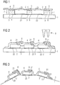
- Example 1 the module is shown before applying the conductive structures.
- the module in Example 1 thus shows a module during the manufacturing process.
- a template 5 is arranged on the side facing away from the carrier substrate 1 side of the module.
- the template 5 is used during the manufacturing step of applying the conductive structures.
- the template 5 is used to structure the conductive structures.
- the template 5 preferably has recesses in the region of the recesses of the electrically insulating layer 4.
- the conductive structures are preferably applied to the electrically insulating layer 4 or to the template 5 by means of a printing process.
- a printing method in particular a screen-printing or pad printing method, a preferably single-layer conductive structure, in particular a metallization layer, can be applied for interconnecting the radiation-emitting semiconductor components 2.
- the structuring of the conductive structures is preferably formed by the template 5 in such a way that the radiation-emitting semiconductor components 2 are electrically conductively connected to one another or to interconnects of the carrier body by means of the conductive structures in a suitable manner.
- the conductive structures electrically connect at least the first contact surface of a radiation-emitting semiconductor component 2 to a further first contact surface of a further radiation-emitting semiconductor component 2 or to a conductor track of the carrier substrate 1 (not illustrated).
- the template 5 is removed.
- the template 5 is thus only temporarily arranged during the manufacturing process on the module.
- FIG. 2 an example of a finished module is shown having conductive structures 8. Unlike the in FIG. 1 The example shows the module FIG. 2 no frame, which is arranged on the carrier substrate 1 and the radiation-emitting semiconductor devices 2 and the planarization layer 3 surrounds.
- the radiation-emitting semiconductor components 2 are preferably fastened on the structured conductor tracks of the carrier substrate 1 by means of a solder or an electrically conductive adhesive.
- an electrically insulating layer 4 is applied to the radiation-emitting components 2 and the planarization layer 3.
- the electrically insulating layer 4 has recesses in areas of the first contact surface 21 of the radiation-emitting semiconductor components 2. These recesses are preferably produced by means of a laser process or a lithography process.
- the conductive structures 8 are applied to the electrically insulating layer 4 by means of a jet printing process.
- the application of the conductive structures 8 is preferably carried out by means of a nozzle 9.
- the nozzle 9 writes the conductive structures, preferably single-layer metal tracks, on the side facing away from the carrier substrate 1 side of the module.
- the conductive structures 8 are applied to the electrically insulating layer 4 in such a way that electrical contacting of the radiation-emitting semiconductor components 2 takes place with one another or with a conductor track of the carrier substrate 1.
- the conductive structures 8 are each in the region of the first contact surface 21 of the radiation-emitting semiconductor components 2.
- the radiation-emitting semiconductor components 2 can thus be grounded separately. Alternatively, the radiation-emitting semiconductor components 2 can be connected to one another in an electrically conductive manner.
- the example of FIG. 3 differs from the example FIG. 2 in that the carrier substrate 1 is a flexible substrate.
- the surface of the carrier substrate 1, on which the radiation-emitting semiconductor components 2 are arranged is not planar.
- the carrier substrate 1 may, for example, have a curvature.
- the surface of the carrier substrate 1 may also have other shapes, as long as it is possible to assemble the radiation-emitting semiconductor components 2.
- the module in the example of the FIG. 3 rotatably mounted. This simplifies with advantage, for example, the production of the module.
- the module can, for example, be moved, for example rotated, in accordance with a desired structuring of the conductive structures.
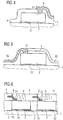
- FIG. 4 a section of an optoelectronic module is shown.
- a radiation-emitting semiconductor component 2 of the module is shown.
- the further radiation-emitting semiconductor components of the module are not shown for the sake of clarity.
- radiation-emitting semiconductor components 2 are preferably adhesively bonded by means of an adhesive layer or soldered by means of a solder.
- an electrically insulating layer 4 is preferably arranged on the radiation-emitting semiconductor components 2 and on the carrier substrate 1.
- the electrically insulating layer 4 is, for example, a laminated film or a layer comprising glass.
- the electrically insulating layer 4 has a recess in the region of the first contact surface 21 of the radiation-emitting semiconductor component 2.
- the electrically insulating layer 4 is preferably a dielectric layer.
- a conductive structure is deposited over the whole area by means of vapor deposition (not shown).
- the whole-area conductive structure is deposited by means of physical or chemical vapor deposition.
- the entire surface formed conductive pattern is structured, for example by means of photolithography and etching in accordance with a desired interconnection of the radiation-emitting semiconductor devices 2.
- the entire-area conductive structure is preferably structured so that the radiation-emitting semiconductor components are electrically conductively connected to one another or a radiation-emitting semiconductor component 2 is electrically conductively connected to a conductor track of the carrier substrate 1.
- the electrically insulating layer in particular the dielectric layer, is preferably planarized prior to the deposition of the conductive structure, for example by means of an SOG method.
- FIG. 5 a section of another optoelectronic module is shown. Also in this case, for the sake of clarity, only a radiation-emitting semiconductor component 2 is shown. Unlike the in FIG. 4 As illustrated, the conductive structure 8 is formed by an anisotropic layer 8a, 8b. Preferably, the anisotropic layer 8a, 8b is an anisotropic film, which is preferably laminated.
- the anisotropic layer preferably has two partial regions 8a, 8b.
- One of the partial regions 8a is preferably conductive.
- another subarea 8b is electrically insulating.
- the formation of the conductivity in the region 8a of the anisotropic layer is preferably carried out by a locally applied pressure or irradiation. As a result, an electrical connection of the radiation-emitting semiconductor component 2 in the region of the first contact surface 21 is advantageously ensured.
- the anistropic layer 8a, 8b is preferably at least partially radiation-transmissive in the second subregion 8b for the radiation emitted by the radiation-emitting semiconductor component 2.
- the Anisotropic layer 8a, 8b are selectively removed in the second portion 8b after lamination. In this case, the anisotropic layer 8a, 8b need not be transparent to radiation.
- FIG. 6 illustrated example of an optoelectronic module has a plurality of radiation-emitting semiconductor devices 2, which are fixed by means of a solder or an adhesive layer 10 on a carrier substrate 1.
- second contact surfaces 22 of the radiation-emitting semiconductor components 2 are in electrical contact with conductor tracks, which are arranged on the carrier substrate 1.
- the interconnects of the radiation-emitting semiconductor components 2 are preferably arranged electrically insulated from one another.
- the electrically insulating layer 4 is formed by a structured printed circuit board and the conductive structures 8 by electrically conductive webs projecting from the printed circuit board, for example metal webs.
- the printed circuit board has an electrically insulating material with electrically conductive strip conductors contained therein.
- the electrically insulating material of the printed circuit board is at least partially transparent to radiation for the radiation emitted by the radiation-emitting semiconductor components 2.
- the electrically insulating material of the printed circuit board may further comprise at least one conversion element to that of the radiation-emitting Semiconductor devices 2 emitted radiation to convert.
- the interconnects contained in the electrically insulating material of the printed circuit board are preferably at least partially electrically connected to the metal webs 8. Furthermore, the metal webs 8 are each preferably electrically conductively connected to the first contact surface 21 of a radiation-emitting semiconductor component 2.
- the printed circuit board 4 in each case has a recess in the region of the first contact surface 21 of a radiation-emitting semiconductor component 2.
- the radiation-emitting semiconductor devices 2 are each contacted electrically.
- the radiation-emitting semiconductor components 2 can be connected to one another in an electrically conductive manner or can be connected to a conductor track of the carrier substrate 1 in an electrically conductive manner.
- the metal webs 8 are preferably shaped such that they are curved from the contact point of the printed circuit board in the direction of the radiation-emitting semiconductor components 2.
- a plurality of circuit boards may be arranged one above the other, so that a multi-layer arrangement and thus multi-layer interconnection levels are formed in the module (not shown).
- the metal webs 8, for example, each with a punch-wedge process with the first contact surface 21 of radiation-emitting semiconductor devices 2 are electrically and mechanically connected.
- FIGS. 7A and 7B in each case a schematic section of an optoelectronic module is shown.
- FIG. 7A represents a cross section of a section of a module.
- FIG. 7B shows a view of the neckline FIG. 7A ,
- FIG. 7A a radiation-emitting semiconductor component 2 is shown.
- An optoelectronic module is preferably composed of a plurality of radiation-emitting semiconductor components 2, which, for example, in FIG. 7A is shown together, wherein the radiation-emitting semiconductor components 2 are preferably arranged on a carrier substrate 1.
- FIG. 7A indicates, in contrast to the examples of FIGS. 1 to 6 , a first contact surface 21, which is guided on the electrically insulating layer 4.
- the electrically insulating layer 4 is guided in each case in regions at the side surfaces of the radiation-emitting semiconductor component 2 around the respective radiation-emitting semiconductor component 2.
- the electrically insulating layer 4 is guided on the side surfaces of the radiation-emitting semiconductor component 2 via the active layer 2 a of the semiconductor component 2.
- the first contact layer 21 is also guided on the side surface of the semiconductor device 2.
- the first contact layer 21 is on the electrically insulating layer 4 out.
- the surface of the radiation-emitting semiconductor component 2 facing away from the carrier substrate is preferably free of the first contact surface 21.
- An electric feed 12 preferably adjoins a region of the first contact layer 21.
- electrical feeds 12 for electrical interconnection of the semiconductor components 2 can be guided at arbitrary regions of the first contact layer 21.
- the semiconductor components of a module can thus be electrically interconnected via the feeders 12.
- the semiconductor devices may be electrically connected separately.
- FIG. 7B is a plan view of the contact guide of a semiconductor device FIG. 7A shown.
- the first contact layer 21 is arranged at the side of a radiation coupling-out surface of the semiconductor component 2.
- the first contact layer 21 is formed like a frame.
- the first contact layer 21 forms a closed path.
- an electrical supply 12 is arranged, which serves to interconnect the semiconductor device 2.
- a current distribution layer 13 is arranged.
- the current distribution layer 13 is at least partially transparent to radiation for the radiation emitted by the semiconductor component 2.
- the current distribution layer 13 is an ITO layer or a ZnO layer.
- the first contact layer 21 is preferably a metallization.
- the radiation coupling-out surface of the semiconductor component 2 is preferably free of the metallization.
- the metallization is led around the semiconductor component 2, whereby a more homogeneous energization is ensured than in, for example, by conventionally used bond pads.
- FIG. 7C is a plan view of a module with a plurality of radiation-emitting semiconductor devices 2 from FIG. 7A shown.
- the module has four radiation-emitting semiconductor components 2.
- an alternative number of semiconductor devices 2 is possible, depending on the particular fields of application and uses of the module.
- the laterally arranged electrical guidance of the first contact surface 21 of the semiconductor components 2 enables complex interconnection of the semiconductor components 2.
- a space-saving arrangement of the semiconductor components 2 on the carrier substrate 1 is thereby advantageously possible.
- the carrier substrate 1 mount and electrically isolated to connect separately.
- the carrier substrate 1 on the mounting side for the semiconductor devices 2 in each case from each other electrically insulated interconnects, on each of which a semiconductor device is mechanically and electrically connected.
- the semiconductor devices 2 may be electrically interconnected.
- the carrier substrate 1 is preferably itself electrically conductive, so that the semiconductor components 2 are at a common electrical potential.
- it can be arranged on the carrier substrate 1, a conductor on which the semiconductor devices 2 are arranged together.
- the electrical leads 12 of the semiconductor devices 2 are preferably led to a further electrical connection (not shown).
- the invention is not limited by the description based on the embodiments of this, but includes any new feature and any combination of features, which in particular includes any combination of features in the claims, even if this feature or combination itself is not explicitly in the claims or Embodiments is given.
Landscapes
- Engineering & Computer Science (AREA)
- Power Engineering (AREA)
- Microelectronics & Electronic Packaging (AREA)
- Computer Hardware Design (AREA)
- Physics & Mathematics (AREA)
- Condensed Matter Physics & Semiconductors (AREA)
- General Physics & Mathematics (AREA)
- Led Device Packages (AREA)
Applications Claiming Priority (2)
| Application Number | Priority Date | Filing Date | Title |
|---|---|---|---|
| DE102008049188A DE102008049188A1 (de) | 2008-09-26 | 2008-09-26 | Optoelektronisches Modul mit einem Trägersubstrat und einer Mehrzahl von strahlungsemittierenden Halbleiterbauelementen und Verfahren zu dessen Herstellung |
| PCT/DE2009/001217 WO2010034278A1 (de) | 2008-09-26 | 2009-08-25 | Optoelektronisches modul mit einem trägersubstrat und einer mehrzahl von strahlungsemittierenden halbleiterbauelementen und verfahren zu dessen herstellung |
Publications (2)
| Publication Number | Publication Date |
|---|---|
| EP2297780A1 EP2297780A1 (de) | 2011-03-23 |
| EP2297780B1 true EP2297780B1 (de) | 2019-06-12 |
Family
ID=41602690
Family Applications (1)
| Application Number | Title | Priority Date | Filing Date |
|---|---|---|---|
| EP09740632.6A Active EP2297780B1 (de) | 2008-09-26 | 2009-08-25 | Optoelektronisches modul mit einem trägersubstrat und einer mehrzahl von strahlung emittierenden halbleiterbauelementen und verfahren zu dessen herstellung |
Country Status (8)
Families Citing this family (12)
| Publication number | Priority date | Publication date | Assignee | Title |
|---|---|---|---|---|
| WO2011145794A1 (ko) | 2010-05-18 | 2011-11-24 | 서울반도체 주식회사 | 파장변환층을 갖는 발광 다이오드 칩과 그 제조 방법, 및 그것을 포함하는 패키지 및 그 제조 방법 |
| DE102010044560A1 (de) * | 2010-09-07 | 2012-03-08 | Osram Opto Semiconductors Gmbh | Verfahren zur Herstellung eines optoelektronischen Halbleiterbauelements |
| DE102011055549A1 (de) | 2011-09-30 | 2013-04-04 | Osram Opto Semiconductors Gmbh | Verfahren zur Herstellung eines optoelektronischen Bauelements mit einer drahtlosen Kontaktierung |
| DE102012209325B4 (de) * | 2012-06-01 | 2021-09-30 | OSRAM Opto Semiconductors Gesellschaft mit beschränkter Haftung | Optoelektronisches Modul |
| US9673254B2 (en) * | 2013-07-22 | 2017-06-06 | Lg Innotek Co., Ltd. | Light emitting device |
| KR101503403B1 (ko) * | 2013-09-09 | 2015-03-17 | 삼성디스플레이 주식회사 | 발광소자모듈 및 그 제조방법 |
| US9195358B1 (en) * | 2014-04-16 | 2015-11-24 | Eastman Kodak Company | Z-fold multi-element substrate structure |
| DE102016208431A1 (de) * | 2016-05-17 | 2017-11-23 | Osram Opto Semiconductors Gmbh | Anordnung mit einem elektrischen Bauteil |
| DE102018120637A1 (de) * | 2018-08-23 | 2020-02-27 | Osram Opto Semiconductors Gmbh | Leiterplatte und verfahren zur herstellung einer leiterplatte mit mindestens einem in die leiterplatte integrierten optoelektronischen bauelement |
| DE102019100794A1 (de) * | 2018-12-20 | 2020-06-25 | Osram Opto Semiconductors Gmbh | Laservorrichtung und verfahren zur herstellung einer laservorrichtung |
| DE102019114315B4 (de) * | 2019-05-28 | 2025-04-17 | OSRAM Opto Semiconductors Gesellschaft mit beschränkter Haftung | Anordnung und verfahren zur herstellung einer anordnung |
| KR102788934B1 (ko) * | 2019-12-06 | 2025-03-31 | 삼성디스플레이 주식회사 | 발광 소자의 정렬 방법, 이를 이용한 표시 장치의 제조 방법 및 표시 장치 |
Citations (1)
| Publication number | Priority date | Publication date | Assignee | Title |
|---|---|---|---|---|
| JP2004172578A (ja) * | 2002-09-02 | 2004-06-17 | Matsushita Electric Ind Co Ltd | 発光装置 |
Family Cites Families (43)
| Publication number | Priority date | Publication date | Assignee | Title |
|---|---|---|---|---|
| JPS55120081A (en) * | 1979-03-08 | 1980-09-16 | Tokyo Shibaura Electric Co | Led display unit |
| JPS575359A (en) * | 1980-06-11 | 1982-01-12 | Hitachi Ltd | Semiconductor device |
| JPS575356A (en) * | 1980-06-13 | 1982-01-12 | Toshiba Corp | Hybrid integrated circuit device |
| JPS61290780A (ja) | 1985-06-19 | 1986-12-20 | Hitachi Vlsi Eng Corp | 光電変換装置 |
| JPH0723827Y2 (ja) * | 1989-06-12 | 1995-05-31 | 株式会社小糸製作所 | 表示装置用光源体 |
| JP2581083Y2 (ja) * | 1991-05-28 | 1998-09-17 | 三洋電機株式会社 | 発光ダイオード表示装置 |
| US5519332A (en) * | 1991-06-04 | 1996-05-21 | Micron Technology, Inc. | Carrier for testing an unpackaged semiconductor die |
| JPH0832112A (ja) * | 1994-07-20 | 1996-02-02 | Toyoda Gosei Co Ltd | 3族窒化物半導体発光素子 |
| DE19638667C2 (de) | 1996-09-20 | 2001-05-17 | Osram Opto Semiconductors Gmbh | Mischfarbiges Licht abstrahlendes Halbleiterbauelement mit Lumineszenzkonversionselement |
| US6529027B1 (en) * | 2000-03-23 | 2003-03-04 | Micron Technology, Inc. | Interposer and methods for fabricating same |
| DE10051159C2 (de) * | 2000-10-16 | 2002-09-19 | Osram Opto Semiconductors Gmbh | LED-Modul, z.B. Weißlichtquelle |
| WO2003012884A1 (en) | 2001-08-01 | 2003-02-13 | Nam-Young Kim | Display system |
| US6784540B2 (en) * | 2001-10-10 | 2004-08-31 | International Rectifier Corp. | Semiconductor device package with improved cooling |
| TW200405790A (en) * | 2002-08-08 | 2004-04-01 | Dainippon Printing Co Ltd | Electromagnetic wave shielding sheet |
| DE10245945A1 (de) * | 2002-09-30 | 2004-04-08 | Osram Opto Semiconductors Gmbh | Lichtquellenmodul sowie Verfahren zu dessen Herstellung |
| DE10353679A1 (de) | 2003-11-17 | 2005-06-02 | Siemens Ag | Kostengünstige, miniaturisierte Aufbau- und Verbindungstechnik für LEDs und andere optoelektronische Module |
| WO2005062389A2 (en) | 2003-12-24 | 2005-07-07 | Matsushita Electric Industrial Co., Ltd. | Semiconductor light emitting device, lighting module, lighting apparatus, display element, and manufacturing method for semiconductor light emitting device |
| US7858994B2 (en) * | 2006-06-16 | 2010-12-28 | Articulated Technologies, Llc | Solid state light sheet and bare die semiconductor circuits with series connected bare die circuit elements |
| DE102004021233A1 (de) * | 2004-04-30 | 2005-12-01 | Osram Opto Semiconductors Gmbh | Leuchtdiodenanordnung |
| US20060035036A1 (en) | 2004-08-16 | 2006-02-16 | Telephus Inc. | Anisotropic conductive adhesive for fine pitch and COG packaged LCD module |
| DE102004050371A1 (de) | 2004-09-30 | 2006-04-13 | Osram Opto Semiconductors Gmbh | Optoelektronisches Bauelement mit einer drahtlosen Kontaktierung |
| TWI277222B (en) * | 2004-10-29 | 2007-03-21 | Lighthouse Technology Co Ltd | LED module and method of packing the same |
| US20060124953A1 (en) * | 2004-12-14 | 2006-06-15 | Negley Gerald H | Semiconductor light emitting device mounting substrates and packages including cavities and cover plates, and methods of packaging same |
| US7563658B2 (en) * | 2004-12-27 | 2009-07-21 | Semiconductor Energy Laboratory Co., Ltd. | Method for manufacturing semiconductor device |
| US7821023B2 (en) * | 2005-01-10 | 2010-10-26 | Cree, Inc. | Solid state lighting component |
| EP2259318A3 (en) * | 2005-02-04 | 2014-01-08 | Seoul Opto Device Co., Ltd. | Light emitting device having a plurality of light emitting cells and method of fabricating the same |
| KR101047683B1 (ko) * | 2005-05-17 | 2011-07-08 | 엘지이노텍 주식회사 | 와이어 본딩이 불필요한 발광소자 패키징 방법 |
| DE102006023123B4 (de) * | 2005-06-01 | 2011-01-13 | Infineon Technologies Ag | Abstandserfassungsradar für Fahrzeuge mit einem Halbleitermodul mit Komponenten für Höchstfrequenztechnik in Kunststoffgehäuse und Verfahren zur Herstellung eines Halbleitermoduls mit Komponenten für ein Abstandserfassungsradar für Fahrzeuge in einem Kunststoffgehäuse |
| EP2750194A1 (en) * | 2005-06-22 | 2014-07-02 | Seoul Viosys Co., Ltd. | Light emitting device comprising a plurality of light emitting diode cells |
| KR100599012B1 (ko) * | 2005-06-29 | 2006-07-12 | 서울옵토디바이스주식회사 | 열전도성 기판을 갖는 발광 다이오드 및 그것을 제조하는방법 |
| TWI285442B (en) * | 2005-08-29 | 2007-08-11 | Gigno Technology Co Ltd | Package structure of light emitting diode |
| US8039849B2 (en) * | 2005-11-23 | 2011-10-18 | Taiwan Oasis Technology Co., Ltd. | LED module |
| JP2007158262A (ja) * | 2005-12-08 | 2007-06-21 | Rohm Co Ltd | 半導体発光素子の製造方法 |
| TWI331406B (en) * | 2005-12-14 | 2010-10-01 | Advanced Optoelectronic Tech | Single chip with multi-led |
| US20070263408A1 (en) * | 2006-05-09 | 2007-11-15 | Chua Janet Bee Y | Backlight module and method of making the module |
| US20100224890A1 (en) * | 2006-09-18 | 2010-09-09 | Cree, Inc. | Light emitting diode chip with electrical insulation element |
| WO2008038910A1 (en) * | 2006-09-25 | 2008-04-03 | Seoul Opto Device Co., Ltd. | Light emitting diode having alingap active layer and method of fabricating the same |
| US7781781B2 (en) * | 2006-11-17 | 2010-08-24 | International Business Machines Corporation | CMOS imager array with recessed dielectric |
| US20080117619A1 (en) * | 2006-11-21 | 2008-05-22 | Siew It Pang | Light source utilizing a flexible circuit carrier and flexible reflectors |
| DE102007009351A1 (de) * | 2007-02-23 | 2008-08-28 | Noctron Holding S.A. | Leuchtmittel |
| DE102007011123A1 (de) * | 2007-03-07 | 2008-09-11 | Osram Opto Semiconductors Gmbh | Licht emittierendes Modul und Herstellungsverfahren für ein Licht emittierendes Modul |
| US8058669B2 (en) * | 2008-08-28 | 2011-11-15 | Taiwan Semiconductor Manufacturing Company, Ltd. | Light-emitting diode integration scheme |
| US8169540B2 (en) * | 2008-09-10 | 2012-05-01 | Panasonic Corporation | Compact camera body to which interchangeable lens unit is mountable |
-
2008
- 2008-09-26 DE DE102008049188A patent/DE102008049188A1/de not_active Withdrawn
-
2009
- 2009-08-25 WO PCT/DE2009/001217 patent/WO2010034278A1/de active Application Filing
- 2009-08-25 US US13/121,128 patent/US8461604B2/en active Active
- 2009-08-25 JP JP2011528181A patent/JP2012503866A/ja active Pending
- 2009-08-25 EP EP09740632.6A patent/EP2297780B1/de active Active
- 2009-08-25 KR KR1020117009227A patent/KR20110057263A/ko not_active Ceased
- 2009-08-25 CN CN2009801381690A patent/CN102165588B/zh active Active
- 2009-09-24 TW TW098132250A patent/TWI438888B/zh active
-
2013
- 2013-06-06 US US13/911,798 patent/US20140030829A1/en not_active Abandoned
Patent Citations (1)
| Publication number | Priority date | Publication date | Assignee | Title |
|---|---|---|---|---|
| JP2004172578A (ja) * | 2002-09-02 | 2004-06-17 | Matsushita Electric Ind Co Ltd | 発光装置 |
Also Published As
| Publication number | Publication date |
|---|---|
| CN102165588A (zh) | 2011-08-24 |
| JP2012503866A (ja) | 2012-02-09 |
| EP2297780A1 (de) | 2011-03-23 |
| DE102008049188A1 (de) | 2010-04-01 |
| CN102165588B (zh) | 2013-09-25 |
| KR20110057263A (ko) | 2011-05-31 |
| WO2010034278A1 (de) | 2010-04-01 |
| US20140030829A1 (en) | 2014-01-30 |
| TWI438888B (zh) | 2014-05-21 |
| US8461604B2 (en) | 2013-06-11 |
| US20110309377A1 (en) | 2011-12-22 |
| TW201019458A (en) | 2010-05-16 |
Similar Documents
| Publication | Publication Date | Title |
|---|---|---|
| EP2297780B1 (de) | Optoelektronisches modul mit einem trägersubstrat und einer mehrzahl von strahlung emittierenden halbleiterbauelementen und verfahren zu dessen herstellung | |
| EP2002176B1 (de) | Optoelektronischer frontscheinwerfer | |
| DE102016119002B4 (de) | Optoelektronisches bauelement und verfahren zum herstellen eines optoelektronischen bauelements | |
| DE102012002605B4 (de) | Verfahren zur Herstellung eines optoelektronischen Halbleiterbauteils und optoelektronisches Halbleiterbauteil | |
| EP2462633A1 (de) | Verfahren zur herstellung eines optoelektronischen halbleiterbauelements und optoelektronisches halbleiterbauelement | |
| DE102004050371A1 (de) | Optoelektronisches Bauelement mit einer drahtlosen Kontaktierung | |
| DE102007046337A1 (de) | Optoelektronischer Halbleiterchip, optoelektronisches Bauelement und Verfahren zum Herstellen eines optoelektronischen Bauelements | |
| WO2009132618A1 (de) | Oberflächenmontierbares leuchtdioden-modul und verfahren zur herstellung eines oberflächenmontierbaren leuchtdioden-moduls | |
| WO2013045353A1 (de) | Led-modul | |
| DE202018004818U1 (de) | Fahrzeugleuchte unter Verwendung eines lichtabstrahlenden Halbleiterbauelements | |
| DE102011011139A1 (de) | Verfahren zur Herstellung zumindest eines optoelektronischen Halbleiterbauelements | |
| DE102013212247B4 (de) | Optoelektronisches Bauelement und Verfahren zu seiner Herstellung | |
| WO2010075831A1 (de) | Verfahren zur fertigung von leuchtmitteln | |
| WO2013124420A1 (de) | Verfahren zum herstellen eines optoelektronischen bauelements und derart hergestelltes optoelektronisches bauelement | |
| DE102006015115A1 (de) | Elektronisches Modul und Verfahren zum Herstellen eines elektronischen Moduls | |
| DE102014116529A1 (de) | Optoelektronisches Halbleiterbauteil und Verfahren zur Herstellung eines optoelektronischen Halbleiterbauteils | |
| WO2017148899A1 (de) | Modul für eine leuchte | |
| WO2012055661A1 (de) | Optoelektronisches halbleiterbauelement mit einem halbleiterchip, einem trägersubstrat und einer folie und ein verfahren zu dessen herstellung | |
| WO2016087360A1 (de) | Verfahren zur herstellung von optoelektronischen modulen und anordnung mit einem solchen modul | |
| DE102008049069B4 (de) | Optoelektronisches Modul mit einem Trägersubstrat, zumindest einem strahlungsemittierenden Halbleiterbauelement und mindestens einem elektrischen Bauelement und Verfahren zu dessen Herstellung | |
| WO2014048699A1 (de) | Optoelektronisches halbleiterbauteil und verfahren zur herstellung eines optoelektronischen halbleiterbauteils | |
| WO2017167792A1 (de) | Verfahren zur herstellung einer vielzahl von halbleiterchips, solcher halbleiterchip und modul mit einem solchen halbleiterchip | |
| DE102012110957A1 (de) | Optoelektronisches Halbleiterbauelement zur Emission von mischfarbiger Strahlung und Verfahren zur Herstellung eines optoelektronischen Halbleiterbauelements | |
| EP2474049B1 (de) | Optoelektronisches modul aufweisend zumindest einen ersten halbleiterkörper mit einer strahlungsaustrittsseite und einer isolationsschicht und verfahren zu dessen herstellung | |
| EP1217664A2 (de) | Halbleiter-Leuchteinheit und Verfahren zur Herstellung derselben |
Legal Events
| Date | Code | Title | Description |
|---|---|---|---|
| PUAI | Public reference made under article 153(3) epc to a published international application that has entered the european phase |
Free format text: ORIGINAL CODE: 0009012 |
|
| 17P | Request for examination filed |
Effective date: 20110131 |
|
| AK | Designated contracting states |
Kind code of ref document: A1 Designated state(s): AT BE BG CH CY CZ DE DK EE ES FI FR GB GR HR HU IE IS IT LI LT LU LV MC MK MT NL NO PL PT RO SE SI SK SM TR |
|
| AX | Request for extension of the european patent |
Extension state: AL BA RS |
|
| DAX | Request for extension of the european patent (deleted) | ||
| STAA | Information on the status of an ep patent application or granted ep patent |
Free format text: STATUS: EXAMINATION IS IN PROGRESS |
|
| 17Q | First examination report despatched |
Effective date: 20180221 |
|
| REG | Reference to a national code |
Ref country code: DE Ref legal event code: R079 Ref document number: 502009015826 Country of ref document: DE Free format text: PREVIOUS MAIN CLASS: H01L0025075000 Ipc: H01L0033620000 |
|
| RIC1 | Information provided on ipc code assigned before grant |
Ipc: H01L 23/00 20060101ALI20190129BHEP Ipc: H01L 25/075 20060101ALI20190129BHEP Ipc: H01L 33/62 20100101AFI20190129BHEP |
|
| GRAP | Despatch of communication of intention to grant a patent |
Free format text: ORIGINAL CODE: EPIDOSNIGR1 |
|
| STAA | Information on the status of an ep patent application or granted ep patent |
Free format text: STATUS: GRANT OF PATENT IS INTENDED |
|
| INTG | Intention to grant announced |
Effective date: 20190318 |
|
| GRAS | Grant fee paid |
Free format text: ORIGINAL CODE: EPIDOSNIGR3 |
|
| GRAA | (expected) grant |
Free format text: ORIGINAL CODE: 0009210 |
|
| STAA | Information on the status of an ep patent application or granted ep patent |
Free format text: STATUS: THE PATENT HAS BEEN GRANTED |
|
| AK | Designated contracting states |
Kind code of ref document: B1 Designated state(s): AT BE BG CH CY CZ DE DK EE ES FI FR GB GR HR HU IE IS IT LI LT LU LV MC MK MT NL NO PL PT RO SE SI SK SM TR |
|
| REG | Reference to a national code |
Ref country code: GB Ref legal event code: FG4D Free format text: NOT ENGLISH |
|
| REG | Reference to a national code |
Ref country code: CH Ref legal event code: EP |
|
| REG | Reference to a national code |
Ref country code: AT Ref legal event code: REF Ref document number: 1143745 Country of ref document: AT Kind code of ref document: T Effective date: 20190615 |
|
| REG | Reference to a national code |
Ref country code: IE Ref legal event code: FG4D Free format text: LANGUAGE OF EP DOCUMENT: GERMAN |
|
| REG | Reference to a national code |
Ref country code: DE Ref legal event code: R096 Ref document number: 502009015826 Country of ref document: DE |
|
| RAP2 | Party data changed (patent owner data changed or rights of a patent transferred) |
Owner name: OSRAM OPTO SEMICONDUCTORS GMBH |
|
| REG | Reference to a national code |
Ref country code: NL Ref legal event code: MP Effective date: 20190612 |
|
| REG | Reference to a national code |
Ref country code: LT Ref legal event code: MG4D |
|
| PG25 | Lapsed in a contracting state [announced via postgrant information from national office to epo] |
Ref country code: LT Free format text: LAPSE BECAUSE OF FAILURE TO SUBMIT A TRANSLATION OF THE DESCRIPTION OR TO PAY THE FEE WITHIN THE PRESCRIBED TIME-LIMIT Effective date: 20190612 Ref country code: HR Free format text: LAPSE BECAUSE OF FAILURE TO SUBMIT A TRANSLATION OF THE DESCRIPTION OR TO PAY THE FEE WITHIN THE PRESCRIBED TIME-LIMIT Effective date: 20190612 Ref country code: ES Free format text: LAPSE BECAUSE OF FAILURE TO SUBMIT A TRANSLATION OF THE DESCRIPTION OR TO PAY THE FEE WITHIN THE PRESCRIBED TIME-LIMIT Effective date: 20190612 Ref country code: FI Free format text: LAPSE BECAUSE OF FAILURE TO SUBMIT A TRANSLATION OF THE DESCRIPTION OR TO PAY THE FEE WITHIN THE PRESCRIBED TIME-LIMIT Effective date: 20190612 Ref country code: NO Free format text: LAPSE BECAUSE OF FAILURE TO SUBMIT A TRANSLATION OF THE DESCRIPTION OR TO PAY THE FEE WITHIN THE PRESCRIBED TIME-LIMIT Effective date: 20190912 Ref country code: SE Free format text: LAPSE BECAUSE OF FAILURE TO SUBMIT A TRANSLATION OF THE DESCRIPTION OR TO PAY THE FEE WITHIN THE PRESCRIBED TIME-LIMIT Effective date: 20190612 |
|
| PG25 | Lapsed in a contracting state [announced via postgrant information from national office to epo] |
Ref country code: GR Free format text: LAPSE BECAUSE OF FAILURE TO SUBMIT A TRANSLATION OF THE DESCRIPTION OR TO PAY THE FEE WITHIN THE PRESCRIBED TIME-LIMIT Effective date: 20190913 Ref country code: LV Free format text: LAPSE BECAUSE OF FAILURE TO SUBMIT A TRANSLATION OF THE DESCRIPTION OR TO PAY THE FEE WITHIN THE PRESCRIBED TIME-LIMIT Effective date: 20190612 Ref country code: BG Free format text: LAPSE BECAUSE OF FAILURE TO SUBMIT A TRANSLATION OF THE DESCRIPTION OR TO PAY THE FEE WITHIN THE PRESCRIBED TIME-LIMIT Effective date: 20190912 |
|
| PG25 | Lapsed in a contracting state [announced via postgrant information from national office to epo] |
Ref country code: EE Free format text: LAPSE BECAUSE OF FAILURE TO SUBMIT A TRANSLATION OF THE DESCRIPTION OR TO PAY THE FEE WITHIN THE PRESCRIBED TIME-LIMIT Effective date: 20190612 Ref country code: SK Free format text: LAPSE BECAUSE OF FAILURE TO SUBMIT A TRANSLATION OF THE DESCRIPTION OR TO PAY THE FEE WITHIN THE PRESCRIBED TIME-LIMIT Effective date: 20190612 Ref country code: NL Free format text: LAPSE BECAUSE OF FAILURE TO SUBMIT A TRANSLATION OF THE DESCRIPTION OR TO PAY THE FEE WITHIN THE PRESCRIBED TIME-LIMIT Effective date: 20190612 Ref country code: RO Free format text: LAPSE BECAUSE OF FAILURE TO SUBMIT A TRANSLATION OF THE DESCRIPTION OR TO PAY THE FEE WITHIN THE PRESCRIBED TIME-LIMIT Effective date: 20190612 Ref country code: CZ Free format text: LAPSE BECAUSE OF FAILURE TO SUBMIT A TRANSLATION OF THE DESCRIPTION OR TO PAY THE FEE WITHIN THE PRESCRIBED TIME-LIMIT Effective date: 20190612 Ref country code: PT Free format text: LAPSE BECAUSE OF FAILURE TO SUBMIT A TRANSLATION OF THE DESCRIPTION OR TO PAY THE FEE WITHIN THE PRESCRIBED TIME-LIMIT Effective date: 20191014 |
|
| PG25 | Lapsed in a contracting state [announced via postgrant information from national office to epo] |
Ref country code: SM Free format text: LAPSE BECAUSE OF FAILURE TO SUBMIT A TRANSLATION OF THE DESCRIPTION OR TO PAY THE FEE WITHIN THE PRESCRIBED TIME-LIMIT Effective date: 20190612 Ref country code: IS Free format text: LAPSE BECAUSE OF FAILURE TO SUBMIT A TRANSLATION OF THE DESCRIPTION OR TO PAY THE FEE WITHIN THE PRESCRIBED TIME-LIMIT Effective date: 20191012 Ref country code: IT Free format text: LAPSE BECAUSE OF FAILURE TO SUBMIT A TRANSLATION OF THE DESCRIPTION OR TO PAY THE FEE WITHIN THE PRESCRIBED TIME-LIMIT Effective date: 20190612 |
|
| REG | Reference to a national code |
Ref country code: DE Ref legal event code: R097 Ref document number: 502009015826 Country of ref document: DE |
|
| PG25 | Lapsed in a contracting state [announced via postgrant information from national office to epo] |
Ref country code: TR Free format text: LAPSE BECAUSE OF FAILURE TO SUBMIT A TRANSLATION OF THE DESCRIPTION OR TO PAY THE FEE WITHIN THE PRESCRIBED TIME-LIMIT Effective date: 20190612 |
|
| PLBE | No opposition filed within time limit |
Free format text: ORIGINAL CODE: 0009261 |
|
| STAA | Information on the status of an ep patent application or granted ep patent |
Free format text: STATUS: NO OPPOSITION FILED WITHIN TIME LIMIT |
|
| PG25 | Lapsed in a contracting state [announced via postgrant information from national office to epo] |
Ref country code: PL Free format text: LAPSE BECAUSE OF FAILURE TO SUBMIT A TRANSLATION OF THE DESCRIPTION OR TO PAY THE FEE WITHIN THE PRESCRIBED TIME-LIMIT Effective date: 20190612 Ref country code: DK Free format text: LAPSE BECAUSE OF FAILURE TO SUBMIT A TRANSLATION OF THE DESCRIPTION OR TO PAY THE FEE WITHIN THE PRESCRIBED TIME-LIMIT Effective date: 20190612 |
|
| 26N | No opposition filed |
Effective date: 20200313 |
|
| PG25 | Lapsed in a contracting state [announced via postgrant information from national office to epo] |
Ref country code: MC Free format text: LAPSE BECAUSE OF FAILURE TO SUBMIT A TRANSLATION OF THE DESCRIPTION OR TO PAY THE FEE WITHIN THE PRESCRIBED TIME-LIMIT Effective date: 20190612 Ref country code: CH Free format text: LAPSE BECAUSE OF NON-PAYMENT OF DUE FEES Effective date: 20190831 Ref country code: IS Free format text: LAPSE BECAUSE OF FAILURE TO SUBMIT A TRANSLATION OF THE DESCRIPTION OR TO PAY THE FEE WITHIN THE PRESCRIBED TIME-LIMIT Effective date: 20200224 Ref country code: LI Free format text: LAPSE BECAUSE OF NON-PAYMENT OF DUE FEES Effective date: 20190831 Ref country code: SI Free format text: LAPSE BECAUSE OF FAILURE TO SUBMIT A TRANSLATION OF THE DESCRIPTION OR TO PAY THE FEE WITHIN THE PRESCRIBED TIME-LIMIT Effective date: 20190612 Ref country code: LU Free format text: LAPSE BECAUSE OF NON-PAYMENT OF DUE FEES Effective date: 20190825 |
|
| REG | Reference to a national code |
Ref country code: BE Ref legal event code: MM Effective date: 20190831 |
|
| PG2D | Information on lapse in contracting state deleted |
Ref country code: IS |
|
| PG25 | Lapsed in a contracting state [announced via postgrant information from national office to epo] |
Ref country code: IE Free format text: LAPSE BECAUSE OF NON-PAYMENT OF DUE FEES Effective date: 20190825 Ref country code: FR Free format text: LAPSE BECAUSE OF NON-PAYMENT OF DUE FEES Effective date: 20190831 Ref country code: IS Free format text: LAPSE BECAUSE OF FAILURE TO SUBMIT A TRANSLATION OF THE DESCRIPTION OR TO PAY THE FEE WITHIN THE PRESCRIBED TIME-LIMIT Effective date: 20191112 |
|
| PG25 | Lapsed in a contracting state [announced via postgrant information from national office to epo] |
Ref country code: BE Free format text: LAPSE BECAUSE OF NON-PAYMENT OF DUE FEES Effective date: 20190831 |
|
| GBPC | Gb: european patent ceased through non-payment of renewal fee |
Effective date: 20190912 |
|
| REG | Reference to a national code |
Ref country code: AT Ref legal event code: MM01 Ref document number: 1143745 Country of ref document: AT Kind code of ref document: T Effective date: 20190825 |
|
| PG25 | Lapsed in a contracting state [announced via postgrant information from national office to epo] |
Ref country code: GB Free format text: LAPSE BECAUSE OF NON-PAYMENT OF DUE FEES Effective date: 20190912 |
|
| PG25 | Lapsed in a contracting state [announced via postgrant information from national office to epo] |
Ref country code: AT Free format text: LAPSE BECAUSE OF NON-PAYMENT OF DUE FEES Effective date: 20190825 |
|
| PG25 | Lapsed in a contracting state [announced via postgrant information from national office to epo] |
Ref country code: CY Free format text: LAPSE BECAUSE OF FAILURE TO SUBMIT A TRANSLATION OF THE DESCRIPTION OR TO PAY THE FEE WITHIN THE PRESCRIBED TIME-LIMIT Effective date: 20190612 |
|
| PG25 | Lapsed in a contracting state [announced via postgrant information from national office to epo] |
Ref country code: MT Free format text: LAPSE BECAUSE OF FAILURE TO SUBMIT A TRANSLATION OF THE DESCRIPTION OR TO PAY THE FEE WITHIN THE PRESCRIBED TIME-LIMIT Effective date: 20190612 Ref country code: HU Free format text: LAPSE BECAUSE OF FAILURE TO SUBMIT A TRANSLATION OF THE DESCRIPTION OR TO PAY THE FEE WITHIN THE PRESCRIBED TIME-LIMIT; INVALID AB INITIO Effective date: 20090825 |
|
| PG25 | Lapsed in a contracting state [announced via postgrant information from national office to epo] |
Ref country code: MK Free format text: LAPSE BECAUSE OF FAILURE TO SUBMIT A TRANSLATION OF THE DESCRIPTION OR TO PAY THE FEE WITHIN THE PRESCRIBED TIME-LIMIT Effective date: 20190612 |
|
| P01 | Opt-out of the competence of the unified patent court (upc) registered |
Effective date: 20230825 |
|
| PGFP | Annual fee paid to national office [announced via postgrant information from national office to epo] |
Ref country code: DE Payment date: 20240821 Year of fee payment: 16 |
|
| REG | Reference to a national code |
Ref country code: DE Ref legal event code: R079 Ref document number: 502009015826 Country of ref document: DE Free format text: PREVIOUS MAIN CLASS: H01L0033620000 Ipc: H10H0020857000 |