EP2294614B1 - Verfahren zur herstellung einer vielzahl von optoelektronischen bauelementen - Google Patents
Verfahren zur herstellung einer vielzahl von optoelektronischen bauelementen Download PDFInfo
- Publication number
- EP2294614B1 EP2294614B1 EP09771994.2A EP09771994A EP2294614B1 EP 2294614 B1 EP2294614 B1 EP 2294614B1 EP 09771994 A EP09771994 A EP 09771994A EP 2294614 B1 EP2294614 B1 EP 2294614B1
- Authority
- EP
- European Patent Office
- Prior art keywords
- semiconductor body
- semiconductor
- layer
- optoelectronic components
- carrier
- Prior art date
- Legal status (The legal status is an assumption and is not a legal conclusion. Google has not performed a legal analysis and makes no representation as to the accuracy of the status listed.)
- Not-in-force
Links
Images


Classifications
-
- H—ELECTRICITY
- H01—ELECTRIC ELEMENTS
- H01L—SEMICONDUCTOR DEVICES NOT COVERED BY CLASS H10
- H01L25/00—Assemblies consisting of a plurality of semiconductor or other solid state devices
- H01L25/03—Assemblies consisting of a plurality of semiconductor or other solid state devices all the devices being of a type provided for in a single subclass of subclasses H10B, H10D, H10F, H10H, H10K or H10N, e.g. assemblies of rectifier diodes
- H01L25/04—Assemblies consisting of a plurality of semiconductor or other solid state devices all the devices being of a type provided for in a single subclass of subclasses H10B, H10D, H10F, H10H, H10K or H10N, e.g. assemblies of rectifier diodes the devices not having separate containers
- H01L25/075—Assemblies consisting of a plurality of semiconductor or other solid state devices all the devices being of a type provided for in a single subclass of subclasses H10B, H10D, H10F, H10H, H10K or H10N, e.g. assemblies of rectifier diodes the devices not having separate containers the devices being of a type provided for in group H10H20/00
- H01L25/0753—Assemblies consisting of a plurality of semiconductor or other solid state devices all the devices being of a type provided for in a single subclass of subclasses H10B, H10D, H10F, H10H, H10K or H10N, e.g. assemblies of rectifier diodes the devices not having separate containers the devices being of a type provided for in group H10H20/00 the devices being arranged next to each other
-
- H—ELECTRICITY
- H01—ELECTRIC ELEMENTS
- H01L—SEMICONDUCTOR DEVICES NOT COVERED BY CLASS H10
- H01L2924/00—Indexing scheme for arrangements or methods for connecting or disconnecting semiconductor or solid-state bodies as covered by H01L24/00
- H01L2924/0001—Technical content checked by a classifier
- H01L2924/0002—Not covered by any one of groups H01L24/00, H01L24/00 and H01L2224/00
-
- H—ELECTRICITY
- H10—SEMICONDUCTOR DEVICES; ELECTRIC SOLID-STATE DEVICES NOT OTHERWISE PROVIDED FOR
- H10H—INORGANIC LIGHT-EMITTING SEMICONDUCTOR DEVICES HAVING POTENTIAL BARRIERS
- H10H20/00—Individual inorganic light-emitting semiconductor devices having potential barriers, e.g. light-emitting diodes [LED]
- H10H20/80—Constructional details
- H10H20/85—Packages
- H10H20/851—Wavelength conversion means
-
- H—ELECTRICITY
- H10—SEMICONDUCTOR DEVICES; ELECTRIC SOLID-STATE DEVICES NOT OTHERWISE PROVIDED FOR
- H10H—INORGANIC LIGHT-EMITTING SEMICONDUCTOR DEVICES HAVING POTENTIAL BARRIERS
- H10H29/00—Integrated devices, or assemblies of multiple devices, comprising at least one light-emitting semiconductor element covered by group H10H20/00
- H10H29/10—Integrated devices comprising at least one light-emitting semiconductor component covered by group H10H20/00
- H10H29/14—Integrated devices comprising at least one light-emitting semiconductor component covered by group H10H20/00 comprising multiple light-emitting semiconductor components
- H10H29/142—Two-dimensional arrangements, e.g. asymmetric LED layout
Definitions
- the invention relates to a method for producing a plurality of optoelectronic components.
- connection carrier For the production of optoelectronic components which are to be fastened and contacted after manufacture on a connection carrier, often a series of individual processing steps are required, which in particular must be carried out individually for the production of each component.
- Patent DE 101 28 271 C1 discloses a method for manufacturing a plurality of optoelectronic devices according to the preamble of claim 1.
- An object of the present invention is to provide a method for producing a plurality of optoelectronic components, which can be produced in a simplified manner.
- a production concept for optoelectronic components has been specified in which the construction of individual optoelectronic components or of a plurality of optoelectronic components combined to form a module takes place at the wafer level level.
- the optoelectronic semiconductor bodies arranged on a semiconductor body carrier are provided with a housing by means of a filling structure.
- a chip sheath can be formed, which consists of a heterogeneous plastic having ceramic-like properties, such as epoxy-silicon mixtures.
- a potting compound which consists of a plastic solid powder mixture. Characteristic of the manufacturing concept is that the filling structure forms a planar layer.
- the step of forming the planar filling structure is carried out by forming a structured resist layer which covers at least the semiconductor body, the planar filling structure is formed outside the patterned resist layer and the structured resist layer is then removed.
- the filling structure serving as a housing is formed by means of a lithographic production method, which allows the lithographic precision customary in the production of semiconductor bodies also to be extended to the production of housing casings.
- the semiconductor body is produced as a luminescence diode chip, preferably as a thin-film luminescence diode chip.
- a functional semiconductor layer sequence comprising, in particular, a radiation-emitting active layer is first epitaxially grown on a growth substrate, then a new support is applied to the surface of the semiconductor layer sequence opposite the growth substrate and subsequently the growth substrate is separated.
- the growth substrates used for nitride compound semiconductors for example SiC, sapphire or GaN, are comparatively expensive, this method offers the particular advantage that the growth substrate can be recycled again.
- the detachment of a growth substrate made of sapphire from a semiconductor layer sequence of a Nitride compound semiconductor can be done for example with a lift-off method.
- the luminescence diode chip may have an epitaxial layer sequence based on a III-V compound semiconductor material, preferably nitride compound semiconductor, but also phosphide compound semiconductor materials or arsenide compound semiconductor materials.
- the epitaxial epitaxial layer sequence or at least one layer thereof comprises a nitride III / V compound semiconductor material, preferably Al x Ga y In 1-xy N, where 0 ⁇ x ⁇ 1 , 0 ⁇ y ⁇ 1 and x + y ⁇ 1.
- This material does not necessarily have to have a mathematically exact composition according to the above formula. Rather, it may comprise one or more dopants as well as additional ingredients that do not substantially alter the characteristic physical properties of the Al x Ga y In 1-xy N material.
- the above formula contains only the essential constituents of the crystal lattice (Al, Ga, In, N), even if these may be partially replaced by small amounts of other substances.
- the active region in particular the semiconductor body, preferably comprises or consists of Al n Ga m In ln P, where 0 ⁇ n ⁇ 1, 0 ⁇ m ⁇ 1 and n + m ⁇ 1, preferably with n ⁇ 0, n ⁇ 1, m ⁇ 0 and / or m ⁇ 1.
- this material does not necessarily have a mathematically exact composition according to the above formula. Rather, it may contain one or more dopants as well as additional Have ingredients that do not substantially alter the physical properties of the material.
- the above formula includes only the essential constituents of the crystal lattice (Al, Ga, In, P), even though these may be partially replaced by small amounts of other substances.
- the active region in particular the semiconductor body, preferably comprises or consists of Al n Ga m In lnm As, where 0 ⁇ n ⁇ 1, 0 ⁇ m ⁇ 1 and n + m ⁇ 1, preferably with n ⁇ 0, n ⁇ 1, m ⁇ 0 and / or m ⁇ 1.
- this material does not necessarily have to have a mathematically exact composition according to the above formula. Rather, it may include one or more dopants as well as additional ingredients that do not substantially alter the physical properties of the material.
- the above formula contains only the essential components of the crystal lattice (Al, Ga, In, As), even though these may be partially replaced by small amounts of other substances.
- the step of providing the semiconductor body carrier comprises that the plurality of semiconductor bodies applied to a semiconductor body carrier are transferred individually from a wafer composite to the semiconductor body carrier.
- the semiconductor body carrier with the plurality of semiconductor bodies can accommodate optoelectronic chip segments of different wafers and assemble into a new composite.
- This is particularly advantageous to different variations in the radiation behavior Semiconductor body to compensate for yield losses or the like.
- it is possible to test the multiplicity of semiconductor bodies beforehand, for example by means of a wafer tester, so that the emission characteristic of the optoelectronic component fulfills certain specifications.
- Another possibility is to arrange semiconductor bodies of different semiconductor wafers on the semiconductor body carrier so that modules with different color impressions or RGB modules can be produced.
- the pick-and-place technologies known in the art may be used.
- the step of providing the semiconductor body carrier comprises that the multiplicity of semiconductor bodies applied to the semiconductor body carrier are transferred together from a wafer composite to the semiconductor body carrier by means of an auxiliary carrier.
- a film may be provided which takes over semiconductor bodies produced on a wafer and deposits them on the semiconductor body carrier.
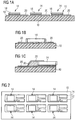
- Figure 1A shows a semiconductor body carrier 10, on which on a first main surface 12, a plurality of semiconductor bodies 14 is applied.
- the semiconductor bodies 14 each have a contact structure 20 which is suitable for electrically contacting the semiconductor body 14.
- the semiconductor body 14, which is arranged above the contact structure 20, comprises an active layer 16, which is embedded in a semiconductor layer sequence 15.
- the active layer 15 is preferably designed for generating radiation.
- the respective semiconductor body is designed as a light-emitting diode semiconductor body.
- the semiconductor body 14 comprises a semiconductor layer sequence 15.
- the semiconductor layer sequence 15 may, for example, comprise two semiconductor layers, between which the active layer 16 is arranged.
- the semiconductor layers are preferably of different conductivity types, in particular doped for different conductivity types (n-type or p-type).
- the semiconductor body 14 is furthermore preferably grown epitaxially.
- a semiconductor layer structure for the semiconductor bodies 14 may be epitaxially deposited on a growth substrate, for example by means of organometallic vapor phase epitaxy. From the semiconductor layer structure then semiconductor body can be formed, for example by means of etching.
- a radiation exit surface 18 is formed, the surface of which corresponds substantially to the size of the semiconductor structure.
- the semiconductor body 14 may be formed, for example, rectangular, wherein the side length of the rectangle may vary over a large area. For example, it is possible to form semiconductor bodies with a side length of less than 50 ⁇ m, but it is also conceivable to use large-area semiconductor bodies with side lengths of up to 5 mm.
- the semiconductor layer sequence 15 has approximately a thickness of, for example, 6 ⁇ m, whereby this value can also vary within a large range.
- the contact structure 20 is metal tracks, for example, of a sputtered metal layer produced by photolithographic techniques. Their thickness is usually a few microns.
- FIG. 1B So is in FIG. 1B a semiconductor body 14 is shown, which has a contact on both side surfaces, which are connected to the contact structure 20. Consequently, the contacts in this embodiment are arranged on opposite sides.
- the semiconductor body 14 is arranged above the semiconductor body carrier 10 and provided on one side with an insulating material 30.
- the connections to the semiconductor layer sequence can then be arranged above or below the insulation material 30.
- the semiconductor bodies 14 are furthermore preferably arranged in accordance with a regular pattern on the semiconductor body carrier 10, as in FIG. 2 is shown. On the basis of in FIG. 2 shown top view, it can be seen that the semiconductor body 14 are arranged for example in the form of a matrix.
- the semiconductor body 14 can be arranged in a freely selectable grid on the semiconductor body carrier 10.
- the multiplicity of the semiconductor bodies 14 can originate, for example, from a wafer composite, wherein the semiconductor bodies 14 are transferred individually to the semiconductor body carrier 10.
- the known in the art pick-and-place method can be used.
- semiconductor body 14 of the wafer composite it is possible to subject semiconductor body 14 of the wafer composite to a test already after production in order, for example, to preselect the semiconductor body 14 to be arranged on semiconductor body carrier 10 with regard to its radiation characteristic.
- semiconductor bodies of different wafer composites which for example have different active layers 16 suitable for generating electromagnetic radiation, so that the semiconductor bodies 14 on the semiconductor body carrier 10 can emit electromagnetic radiation having different wavelengths.
- auxiliary carrier for example a foil, preferably a thermorelease foil.
- individual processing steps are saved.
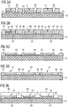
- FIGS. 3A to 3B a first embodiment for producing a plurality of optoelectronic devices described.
- the starting point of the method are the in FIGS. 1A to 1C described semiconductor body 14, which are arranged on the semiconductor body carrier 10.
- a photoresist layer is applied in a first step, which is subsequently patterned.
- the patterning of the photoresist layer can be carried out, for example, with the photolithographic exposure known in the art.
- a photoresist pattern 40 covering the semiconductor bodies 14 and parts of the contact structure 20 is obtained.
- the photoresist layer is structured in such a way that teaching areas arise on the sides of the semiconductor bodies 14.
- the photoresist layer is also removed between contact structures 20 of adjacent semiconductor bodies.
- the semiconductor body carrier 10 a variety of materials can be used. For example, it is intended to use a ceramic substrate or a silicon substrate. Other possible materials include magnesium oxide, alumina, sapphire, aluminum nitride, or other materials known to those skilled in the art.
- the filling structure 42 has a substantially identical height as the resist pattern 40.
- the filler material may be, for example, a plastic.
- benzocyclobutenes are used.
- the resist pattern 40 is removed and a further planarization step is performed.
- the further planarization step reduces the height of the filling structure 42 so that now a filling structure 44 which is planar with the upper side of the semiconductor body 14 is formed.
- the further process steps include the formation of protective diodes, the application of a converter, the formation of reflector layers or the application of optical elements, such as lenses. It should be noted, however, that these additional process steps do not necessarily all have to be performed. For example, it is conceivable to produce optoelectronic components which do not require a converter or are operated without protective diodes. Consequently, the process steps shown below are only to be understood as examples.
- protective diodes 46 are shown, which are arranged on the connection carrier 20 on the corresponding first contact surfaces 21 and second contact surfaces 22. Furthermore, in this process step, the electrical wiring is performed.
- the converter layer is, for example, a silicone layer in which at least one luminescence conversion substance is embedded.
- the at least one luminescence conversion substance may be for example YAG: Ce or a known Lumineszenzkonversionsstoff act.
- silicone layer as a carrier layer for the luminescence conversion substance has the advantage that silicone is comparatively insensitive to short-wave blue or ultraviolet radiation. This is particularly advantageous for luminescence diode chips based on nitride compound semiconductors, in which the emitted radiation usually contains at least a portion of the short-wave blue or ultraviolet spectral range.
- another transparent organic or inorganic material can act as a carrier layer for the at least one luminescence conversion substance.
- Further process steps include the application of a contact layer as a reflective contact layer.
- a barrier layer can be arranged between a contact layer 20 and a connection layer.
- the barrier layer contains, for example, TiWN.
- a diffusion of material of the bonding layer which is a solder layer for example, is prevented by the barrier layer into the reflective contact layer, which could impair the reflection of the reflective contact layer, in particular.
- the converter can be provided, for example, on a carrier film and transferred in a single step to a semiconductor body of the plurality of optoelectronic components. Consequently, time-consuming individual processing steps are saved on individual optoelectronic components.
- the converter material of the converter 48 different manufacturing methods are known in the art.
- the method according to the FIGS. 4A to 4E differs from the method described above in that the step of further planarizing the filling structure is eliminated. Consequently, the resist pattern protrudes beyond the radiation exit surface of the semiconductor body, so that a cavity is formed above it.
- This cavity can be used in the following as in FIG. 4C is shown to fill the converter 48.
- a converter material is advantageously used, which is present in a liquid state of aggregation and cures after filling into the cavities. Furthermore, it is also provided to leave a gap between the radiation exit surface and the converter or to provide a cover. This has particular thermal benefits Use of optoelectronic components which emit radiation in the ultraviolet range.
- FIG. 4D Another variant concerns the Figure 4D , There it is shown to contact the contact surfaces 21, 22 of the contact structure 20 of the first main surface 12 opposite side by means of vias 54 (so-called vias). Accordingly, it is possible to produce optoelectronic devices suitable for surface mounting.
- FIG. 3 or 4 not shown variant relates to the formation of protective diodes.
- a protective diode can be formed directly in the semiconductor body 10, for example by suitable doping.
- the electrical characteristic of the protective diode can be adapted to the particular application.
- the optics may consist of a plurality of lenses 52 which are arranged on a carrier 50. Accordingly, a lens 52 is now formed for each of the optoelectronic semiconductor bodies on the semiconductor body carrier 10 in a single process step.
- FIGS. 5A and 5B a further embodiment of the invention shown.
- the process steps shown here follow the method steps according to FIGS FIGS. 3A to 3E or FIGS. 4A to 4E at.
- modules may be formed which contain one or two LED chips.
- cuts are made through the filling material between adjacent semiconductor bodies 14, as in FIG. 5B is shown schematically by the section lines 61 and 62.
- FIG. 6 is in a further embodiment, the assembly with protective diodes 46 explained in more detail.
- the protective diodes 46 are arranged, for example, by means of a surface mounting method on the first contact surfaces 21 and the second contact surfaces 22.
- the attachment of the protective diodes 46 is advantageously carried out before the separation of the optoelectronic components.
- This variant relates to the application of the filling material, which consists of a potting compound according to this embodiment.
- the semiconductor body carrier 10 is provided with the potting compound 70. This can be applied, for example, in drop form.
- the semiconductor body carrier 10 is inserted between two workpieces 72 and 74, wherein the two workpieces are heated.
- the upper workpiece 74 has an opening (cavity) so as not to touch the semiconductor bodies 14 on the semiconductor body carrier 10.
- the potting compound 70 is now pressed between the semiconductor body 14.
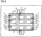
- FIG. 8 a further embodiment is shown, in which the plurality of optoelectronic components is mounted on a common connection carrier.
- the outer semiconductor body 14 are each provided with pads 21 and 22 respectively.
- the semiconductor body lying in the interior of the arrangement is guided on a contact pad 23 by means of a bridging contact 84, which runs over the conductor track of the chip arranged above it.
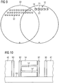
- FIG. 9 illustrates where a semiconductor substrate 10 is shown comprising a plurality of optoelectronic devices.
- the semiconductor substrate carrier 10 may be a 6 "wafer, and on the left side there are shown a plurality of lenses fabricated in the wafer assembly, thus allowing, for example, the attachment of optical elements over the semiconductor body 14 in a single step to perform a plurality of optoelectronic components on a semiconductor body carrier.
- FIG. 10 Another embodiment is with reference to FIG. 10 shown.
- a so-called stacked semiconductor body is used, which consists for example of three semiconductor layer sequences, which are each provided with different active layers, for example, to form red, green or blue radiating semiconductor body.
- a passivation layer can be arranged on the side flanks of this layer stack.
- the flank angle of the side edges of the filling material can be variable.
- passivation layers 92 or the mirrors arranged on the side edges it is possible to use a process control which is similar to that in FIGS FIGS. 3A to 3E or 4A to 4E runs.
- this process differs in that the example in FIG. 3A shown structuring of the resist layer is performed so that the resist layer also covers the edges of the semiconductor body 14. Consequently, after the removal of the resist structure between the semiconductor body 14 and the filling structure, a gap is created in which the passivation or the mirrors can be introduced.
Landscapes
- Engineering & Computer Science (AREA)
- Power Engineering (AREA)
- Microelectronics & Electronic Packaging (AREA)
- Physics & Mathematics (AREA)
- Condensed Matter Physics & Semiconductors (AREA)
- General Physics & Mathematics (AREA)
- Computer Hardware Design (AREA)
- Led Devices (AREA)
- Led Device Packages (AREA)
Applications Claiming Priority (2)
| Application Number | Priority Date | Filing Date | Title |
|---|---|---|---|
| DE102008030815A DE102008030815A1 (de) | 2008-06-30 | 2008-06-30 | Verfahren zur Herstellung einer Vielzahl von optoelektronischen Bauelementen |
| PCT/DE2009/000857 WO2010000224A2 (de) | 2008-06-30 | 2009-06-18 | Verfahren zur herstellung einer vielzahl von optoelektronischen bauelementen |
Publications (2)
| Publication Number | Publication Date |
|---|---|
| EP2294614A2 EP2294614A2 (de) | 2011-03-16 |
| EP2294614B1 true EP2294614B1 (de) | 2017-11-22 |
Family
ID=41228784
Family Applications (1)
| Application Number | Title | Priority Date | Filing Date |
|---|---|---|---|
| EP09771994.2A Not-in-force EP2294614B1 (de) | 2008-06-30 | 2009-06-18 | Verfahren zur herstellung einer vielzahl von optoelektronischen bauelementen |
Country Status (7)
| Country | Link |
|---|---|
| US (1) | US8431422B2 (enExample) |
| EP (1) | EP2294614B1 (enExample) |
| JP (1) | JP5693450B2 (enExample) |
| KR (1) | KR101587299B1 (enExample) |
| CN (1) | CN101983428B (enExample) |
| DE (1) | DE102008030815A1 (enExample) |
| WO (1) | WO2010000224A2 (enExample) |
Families Citing this family (10)
| Publication number | Priority date | Publication date | Assignee | Title |
|---|---|---|---|---|
| US8816383B2 (en) * | 2012-07-06 | 2014-08-26 | Invensas Corporation | High performance light emitting diode with vias |
| DE102012217776A1 (de) | 2012-09-28 | 2014-06-12 | Osram Opto Semiconductors Gmbh | Verfahren zur Herstellung eines optoelektronischen Bauelements |
| DE102013107862A1 (de) | 2013-07-23 | 2015-01-29 | Osram Opto Semiconductors Gmbh | Oberflächenmontierbares optoelektronisches Halbleiterbauteil und Verfahren zur Herstellung zumindest eines oberflächenmontierbaren optoelektronischen Halbleiterbauteils |
| DE102014114188B4 (de) * | 2014-09-30 | 2022-01-20 | Osram Gmbh | Verfahren zur Herstellung eines optoelektronischen Halbleiterbauteils |
| DE102015103835A1 (de) * | 2015-03-16 | 2016-09-22 | Osram Opto Semiconductors Gmbh | Lichtemittierendes Bauelement und Verfahren zur Herstellung eines lichtemittierenden Bauelements |
| JP6217711B2 (ja) | 2015-08-21 | 2017-10-25 | 日亜化学工業株式会社 | 発光装置の製造方法 |
| TWI688121B (zh) | 2018-08-24 | 2020-03-11 | 隆達電子股份有限公司 | 發光二極體結構 |
| US11038088B2 (en) | 2019-10-14 | 2021-06-15 | Lextar Electronics Corporation | Light emitting diode package |
| CN111883552B (zh) * | 2020-08-04 | 2023-09-05 | 厦门乾照光电股份有限公司 | 一种集成式led芯片模组及其制作、测试、切割方法 |
| CN118472152B (zh) * | 2024-07-12 | 2024-09-17 | 诺视科技(浙江)有限公司 | 集成反射穹顶的微显示器件及其制备方法 |
Family Cites Families (26)
| Publication number | Priority date | Publication date | Assignee | Title |
|---|---|---|---|---|
| US5104824A (en) * | 1990-11-06 | 1992-04-14 | Bell Communications Research, Inc. | Selective area regrowth for surface-emitting lasers and other sharp features |
| JPH11177138A (ja) * | 1997-12-11 | 1999-07-02 | Stanley Electric Co Ltd | 面実装型装置およびこれを用いた発光装置または受光装置 |
| JP3829594B2 (ja) * | 2000-06-30 | 2006-10-04 | セイコーエプソン株式会社 | 素子実装方法と光伝送装置 |
| US6432752B1 (en) * | 2000-08-17 | 2002-08-13 | Micron Technology, Inc. | Stereolithographic methods for fabricating hermetic semiconductor device packages and semiconductor devices including stereolithographically fabricated hermetic packages |
| TW473951B (en) | 2001-01-17 | 2002-01-21 | Siliconware Precision Industries Co Ltd | Non-leaded quad flat image sensor package |
| DE10128271C1 (de) * | 2001-06-12 | 2002-11-28 | Liz Electronics Corp | Verfahren zur Herstellung von Dioden |
| DE10222609B4 (de) * | 2002-04-15 | 2008-07-10 | Schott Ag | Verfahren zur Herstellung strukturierter Schichten auf Substraten und verfahrensgemäß beschichtetes Substrat |
| DE10235332A1 (de) * | 2002-08-01 | 2004-02-19 | Infineon Technologies Ag | Mehrlagiger Schaltungsträger und Herstellung desselben |
| DE10245930A1 (de) * | 2002-09-30 | 2004-04-08 | Osram Opto Semiconductors Gmbh | Optoelektronisches Bauelement und Bauelement-Modul |
| JP4603368B2 (ja) * | 2003-02-28 | 2010-12-22 | オスラム オプト セミコンダクターズ ゲゼルシャフト ミット ベシュレンクテル ハフツング | 構造化された金属被覆を施されたパッケージボディを有するオプトエレクトロニクス素子、この種の素子を製作する方法、およびプラスチックを含むボディに、構造化された金属被覆を施す方法 |
| JP2004304161A (ja) * | 2003-03-14 | 2004-10-28 | Sony Corp | 発光素子、発光装置、画像表示装置、発光素子の製造方法及び画像表示装置の製造方法 |
| US20070126016A1 (en) * | 2005-05-12 | 2007-06-07 | Epistar Corporation | Light emitting device and manufacture method thereof |
| US7084496B2 (en) * | 2004-01-14 | 2006-08-01 | International Business Machines Corporation | Method and apparatus for providing optoelectronic communication with an electronic device |
| AU2005232074A1 (en) * | 2004-03-29 | 2005-10-20 | LumaChip, Inc. | Roll-to-roll fabricated light sheet and encapsulated semiconductor circuit devices |
| DE102004021233A1 (de) * | 2004-04-30 | 2005-12-01 | Osram Opto Semiconductors Gmbh | Leuchtdiodenanordnung |
| JP2006108204A (ja) * | 2004-10-01 | 2006-04-20 | Renesas Technology Corp | 半導体モジュール及び電子装置 |
| DE102006032047A1 (de) * | 2006-07-10 | 2008-01-24 | Schott Ag | Verfahren zur Herstellung optoelektronischer Bauelemente und damit hergestellte Erzeugnisse |
| JP2008027999A (ja) * | 2006-07-19 | 2008-02-07 | Matsushita Electric Ind Co Ltd | 発光装置の製造方法および発光装置 |
| DE102007004303A1 (de) | 2006-08-04 | 2008-02-07 | Osram Opto Semiconductors Gmbh | Dünnfilm-Halbleiterbauelement und Bauelement-Verbund |
| DE102006051746A1 (de) * | 2006-09-29 | 2008-04-03 | Osram Opto Semiconductors Gmbh | Optoelektronisches Bauelement mit einer Lumineszenzkonversionsschicht |
| WO2008086090A1 (en) * | 2007-01-05 | 2008-07-17 | University Of Washington | Self-assembled heterogeneous integrated optical analysis system |
| DE102007008524A1 (de) * | 2007-02-21 | 2008-08-28 | Osram Opto Semiconductors Gmbh | Strahlung emittierender Chip mit mindestens einem Halbleiterkörper |
| DE102007030129A1 (de) * | 2007-06-29 | 2009-01-02 | Osram Opto Semiconductors Gmbh | Verfahren zur Herstellung einer Mehrzahl optoelektronischer Bauelemente und optoelektronisches Bauelement |
| DE102007043877A1 (de) | 2007-06-29 | 2009-01-08 | Osram Opto Semiconductors Gmbh | Verfahren zur Herstellung von optoelektronischen Bauelementen und optoelektronisches Bauelement |
| DE102008013030A1 (de) | 2007-12-14 | 2009-06-25 | Osram Opto Semiconductors Gmbh | Strahlungsemittierende Vorrichtung |
| DE102008014094A1 (de) | 2008-03-13 | 2009-09-17 | Osram Opto Semiconductors Gmbh | Strahlungsemittierende Vorrichtung und Verfahren zur Herstellung einer strahlungsemittierenden Vorrichtung |
-
2008
- 2008-06-30 DE DE102008030815A patent/DE102008030815A1/de not_active Withdrawn
-
2009
- 2009-06-18 CN CN2009801119833A patent/CN101983428B/zh not_active Expired - Fee Related
- 2009-06-18 JP JP2011515089A patent/JP5693450B2/ja not_active Expired - Fee Related
- 2009-06-18 EP EP09771994.2A patent/EP2294614B1/de not_active Not-in-force
- 2009-06-18 WO PCT/DE2009/000857 patent/WO2010000224A2/de not_active Ceased
- 2009-06-18 KR KR1020107020383A patent/KR101587299B1/ko not_active Expired - Fee Related
- 2009-06-18 US US12/922,397 patent/US8431422B2/en not_active Expired - Fee Related
Also Published As
| Publication number | Publication date |
|---|---|
| DE102008030815A1 (de) | 2009-12-31 |
| CN101983428B (zh) | 2013-06-12 |
| KR101587299B1 (ko) | 2016-02-02 |
| WO2010000224A2 (de) | 2010-01-07 |
| JP2011526418A (ja) | 2011-10-06 |
| WO2010000224A3 (de) | 2010-03-04 |
| JP5693450B2 (ja) | 2015-04-01 |
| US8431422B2 (en) | 2013-04-30 |
| KR20110025164A (ko) | 2011-03-09 |
| EP2294614A2 (de) | 2011-03-16 |
| US20110086447A1 (en) | 2011-04-14 |
| CN101983428A (zh) | 2011-03-02 |
Similar Documents
| Publication | Publication Date | Title |
|---|---|---|
| EP2294614B1 (de) | Verfahren zur herstellung einer vielzahl von optoelektronischen bauelementen | |
| EP2162927B1 (de) | Verfahren zur herstellung von optoelektronischen bauelementen | |
| EP2162928B1 (de) | Verfahren zur herstellung einer mehrzahl optoelektronischer bauelemente und optoelektronisches bauelement | |
| DE102009056386B4 (de) | Verfahren zur Herstellung eines Halbleiterbauelements | |
| DE112012005357B4 (de) | Anzeigevorrichtung und Verfahren zur Herstellung einer Anzeigevorrichtung | |
| DE102012109460B4 (de) | Verfahren zur Herstellung eines Leuchtdioden-Displays und Leuchtdioden-Display | |
| DE102010034665B4 (de) | Optoelektronischer Halbleiterchip und Verfahren zur Herstellung von optoelektronischen Halbleiterchips | |
| DE112016000533B4 (de) | Verfahren zur Herstellung eines Halbleiterbauelements und Halbleiterbauelement | |
| EP2901479B1 (de) | Optoelektronisches bauelement | |
| EP2193553A1 (de) | Optoelektronischer halbleiterchip, optoelektronisches bauelement und verfahren zum herstellen eines optoelektronischen bauelements | |
| DE102013111496A1 (de) | Verfahren zum Herstellen von optoelektronischen Halbleiterbauelementen und optoelektronisches Halbleiterbauelement | |
| WO2015121062A1 (de) | Verfahren zur herstellung eines optoelektronischen halbleiterbauteils sowie optoelektronisches halbleiterbauteil | |
| DE102004025684B4 (de) | Verfahren zum Ausbilden einer Kontaktstruktur zur elektrischen Kontaktierung eines optoelektronischen Halbleiterchips | |
| WO2018234154A1 (de) | Optoelektronisches halbleiterbauelement | |
| WO2020074351A1 (de) | Optoelektronisches halbleiterbauteil | |
| EP3327796B1 (de) | Optoelektronisches bauelement und verfahren zur herstellung eines optoelektronischen bauelements | |
| WO2013029862A1 (de) | Verfahren zur herstellung einer leuchtdiode und leuchtdiode | |
| EP2304816B1 (de) | Elektrolumineszierende vorrichtung und verfahren zur herstellung einer elektrolumineszierenden vorrichtung | |
| EP2283527A1 (de) | Strahlung emittierender dünnfilm-halbleiterchip und verfahren zur herstellung eines strahlung emittierenden dünnfilm-halbleiterchips | |
| WO2021023577A1 (de) | Verfahren zur vereinzelung von bauteilen aus einem bauteilverbund sowie bauteil | |
| WO2019175205A1 (de) | Optoelektronisches bauelement und dessen herstellungsverfahren | |
| WO2019175168A1 (de) | Multipixelchip und verfahren zur herstellung eines multipixelchips | |
| WO2016198620A1 (de) | Verfahren zur herstellung von optoelektronischen konversions-halbleiterchips und verbund von konversions-halbleiterchips | |
| DE102016103353B4 (de) | Verfahren zur Herstellung eines optoelektronischen Bauelements |
Legal Events
| Date | Code | Title | Description |
|---|---|---|---|
| PUAI | Public reference made under article 153(3) epc to a published international application that has entered the european phase |
Free format text: ORIGINAL CODE: 0009012 |
|
| 17P | Request for examination filed |
Effective date: 20100906 |
|
| AK | Designated contracting states |
Kind code of ref document: A2 Designated state(s): AT BE BG CH CY CZ DE DK EE ES FI FR GB GR HR HU IE IS IT LI LT LU LV MC MK MT NL NO PL PT RO SE SI SK TR |
|
| AX | Request for extension of the european patent |
Extension state: AL BA RS |
|
| DAX | Request for extension of the european patent (deleted) | ||
| 17Q | First examination report despatched |
Effective date: 20160301 |
|
| GRAP | Despatch of communication of intention to grant a patent |
Free format text: ORIGINAL CODE: EPIDOSNIGR1 |
|
| INTG | Intention to grant announced |
Effective date: 20170612 |
|
| GRAS | Grant fee paid |
Free format text: ORIGINAL CODE: EPIDOSNIGR3 |
|
| GRAA | (expected) grant |
Free format text: ORIGINAL CODE: 0009210 |
|
| AK | Designated contracting states |
Kind code of ref document: B1 Designated state(s): AT BE BG CH CY CZ DE DK EE ES FI FR GB GR HR HU IE IS IT LI LT LU LV MC MK MT NL NO PL PT RO SE SI SK TR |
|
| REG | Reference to a national code |
Ref country code: GB Ref legal event code: FG4D Free format text: NOT ENGLISH |
|
| REG | Reference to a national code |
Ref country code: CH Ref legal event code: EP |
|
| REG | Reference to a national code |
Ref country code: IE Ref legal event code: FG4D Free format text: LANGUAGE OF EP DOCUMENT: GERMAN |
|
| REG | Reference to a national code |
Ref country code: AT Ref legal event code: REF Ref document number: 949145 Country of ref document: AT Kind code of ref document: T Effective date: 20171215 |
|
| REG | Reference to a national code |
Ref country code: DE Ref legal event code: R096 Ref document number: 502009014547 Country of ref document: DE |
|
| REG | Reference to a national code |
Ref country code: NL Ref legal event code: MP Effective date: 20171122 |
|
| REG | Reference to a national code |
Ref country code: LT Ref legal event code: MG4D |
|
| PG25 | Lapsed in a contracting state [announced via postgrant information from national office to epo] |
Ref country code: LT Free format text: LAPSE BECAUSE OF FAILURE TO SUBMIT A TRANSLATION OF THE DESCRIPTION OR TO PAY THE FEE WITHIN THE PRESCRIBED TIME-LIMIT Effective date: 20171122 Ref country code: SE Free format text: LAPSE BECAUSE OF FAILURE TO SUBMIT A TRANSLATION OF THE DESCRIPTION OR TO PAY THE FEE WITHIN THE PRESCRIBED TIME-LIMIT Effective date: 20171122 Ref country code: FI Free format text: LAPSE BECAUSE OF FAILURE TO SUBMIT A TRANSLATION OF THE DESCRIPTION OR TO PAY THE FEE WITHIN THE PRESCRIBED TIME-LIMIT Effective date: 20171122 Ref country code: NO Free format text: LAPSE BECAUSE OF FAILURE TO SUBMIT A TRANSLATION OF THE DESCRIPTION OR TO PAY THE FEE WITHIN THE PRESCRIBED TIME-LIMIT Effective date: 20180222 Ref country code: ES Free format text: LAPSE BECAUSE OF FAILURE TO SUBMIT A TRANSLATION OF THE DESCRIPTION OR TO PAY THE FEE WITHIN THE PRESCRIBED TIME-LIMIT Effective date: 20171122 Ref country code: NL Free format text: LAPSE BECAUSE OF FAILURE TO SUBMIT A TRANSLATION OF THE DESCRIPTION OR TO PAY THE FEE WITHIN THE PRESCRIBED TIME-LIMIT Effective date: 20171122 |
|
| PG25 | Lapsed in a contracting state [announced via postgrant information from national office to epo] |
Ref country code: HR Free format text: LAPSE BECAUSE OF FAILURE TO SUBMIT A TRANSLATION OF THE DESCRIPTION OR TO PAY THE FEE WITHIN THE PRESCRIBED TIME-LIMIT Effective date: 20171122 Ref country code: GR Free format text: LAPSE BECAUSE OF FAILURE TO SUBMIT A TRANSLATION OF THE DESCRIPTION OR TO PAY THE FEE WITHIN THE PRESCRIBED TIME-LIMIT Effective date: 20180223 Ref country code: LV Free format text: LAPSE BECAUSE OF FAILURE TO SUBMIT A TRANSLATION OF THE DESCRIPTION OR TO PAY THE FEE WITHIN THE PRESCRIBED TIME-LIMIT Effective date: 20171122 Ref country code: BG Free format text: LAPSE BECAUSE OF FAILURE TO SUBMIT A TRANSLATION OF THE DESCRIPTION OR TO PAY THE FEE WITHIN THE PRESCRIBED TIME-LIMIT Effective date: 20180222 |
|
| PG25 | Lapsed in a contracting state [announced via postgrant information from national office to epo] |
Ref country code: DK Free format text: LAPSE BECAUSE OF FAILURE TO SUBMIT A TRANSLATION OF THE DESCRIPTION OR TO PAY THE FEE WITHIN THE PRESCRIBED TIME-LIMIT Effective date: 20171122 Ref country code: SK Free format text: LAPSE BECAUSE OF FAILURE TO SUBMIT A TRANSLATION OF THE DESCRIPTION OR TO PAY THE FEE WITHIN THE PRESCRIBED TIME-LIMIT Effective date: 20171122 Ref country code: CZ Free format text: LAPSE BECAUSE OF FAILURE TO SUBMIT A TRANSLATION OF THE DESCRIPTION OR TO PAY THE FEE WITHIN THE PRESCRIBED TIME-LIMIT Effective date: 20171122 Ref country code: CY Free format text: LAPSE BECAUSE OF FAILURE TO SUBMIT A TRANSLATION OF THE DESCRIPTION OR TO PAY THE FEE WITHIN THE PRESCRIBED TIME-LIMIT Effective date: 20171122 Ref country code: EE Free format text: LAPSE BECAUSE OF FAILURE TO SUBMIT A TRANSLATION OF THE DESCRIPTION OR TO PAY THE FEE WITHIN THE PRESCRIBED TIME-LIMIT Effective date: 20171122 |
|
| REG | Reference to a national code |
Ref country code: DE Ref legal event code: R097 Ref document number: 502009014547 Country of ref document: DE |
|
| PG25 | Lapsed in a contracting state [announced via postgrant information from national office to epo] |
Ref country code: PL Free format text: LAPSE BECAUSE OF FAILURE TO SUBMIT A TRANSLATION OF THE DESCRIPTION OR TO PAY THE FEE WITHIN THE PRESCRIBED TIME-LIMIT Effective date: 20171122 Ref country code: RO Free format text: LAPSE BECAUSE OF FAILURE TO SUBMIT A TRANSLATION OF THE DESCRIPTION OR TO PAY THE FEE WITHIN THE PRESCRIBED TIME-LIMIT Effective date: 20171122 Ref country code: IT Free format text: LAPSE BECAUSE OF FAILURE TO SUBMIT A TRANSLATION OF THE DESCRIPTION OR TO PAY THE FEE WITHIN THE PRESCRIBED TIME-LIMIT Effective date: 20171122 |
|
| PG25 | Lapsed in a contracting state [announced via postgrant information from national office to epo] |
Ref country code: MT Free format text: LAPSE BECAUSE OF FAILURE TO SUBMIT A TRANSLATION OF THE DESCRIPTION OR TO PAY THE FEE WITHIN THE PRESCRIBED TIME-LIMIT Effective date: 20171122 |
|
| PLBE | No opposition filed within time limit |
Free format text: ORIGINAL CODE: 0009261 |
|
| STAA | Information on the status of an ep patent application or granted ep patent |
Free format text: STATUS: NO OPPOSITION FILED WITHIN TIME LIMIT |
|
| 26N | No opposition filed |
Effective date: 20180823 |
|
| PG25 | Lapsed in a contracting state [announced via postgrant information from national office to epo] |
Ref country code: SI Free format text: LAPSE BECAUSE OF FAILURE TO SUBMIT A TRANSLATION OF THE DESCRIPTION OR TO PAY THE FEE WITHIN THE PRESCRIBED TIME-LIMIT Effective date: 20171122 |
|
| REG | Reference to a national code |
Ref country code: CH Ref legal event code: PL |
|
| GBPC | Gb: european patent ceased through non-payment of renewal fee |
Effective date: 20180618 |
|
| REG | Reference to a national code |
Ref country code: BE Ref legal event code: MM Effective date: 20180630 |
|
| REG | Reference to a national code |
Ref country code: IE Ref legal event code: MM4A |
|
| PG25 | Lapsed in a contracting state [announced via postgrant information from national office to epo] |
Ref country code: MC Free format text: LAPSE BECAUSE OF FAILURE TO SUBMIT A TRANSLATION OF THE DESCRIPTION OR TO PAY THE FEE WITHIN THE PRESCRIBED TIME-LIMIT Effective date: 20171122 Ref country code: LU Free format text: LAPSE BECAUSE OF NON-PAYMENT OF DUE FEES Effective date: 20180618 |
|
| PG25 | Lapsed in a contracting state [announced via postgrant information from national office to epo] |
Ref country code: LI Free format text: LAPSE BECAUSE OF NON-PAYMENT OF DUE FEES Effective date: 20180630 Ref country code: IE Free format text: LAPSE BECAUSE OF NON-PAYMENT OF DUE FEES Effective date: 20180618 Ref country code: GB Free format text: LAPSE BECAUSE OF NON-PAYMENT OF DUE FEES Effective date: 20180618 Ref country code: CH Free format text: LAPSE BECAUSE OF NON-PAYMENT OF DUE FEES Effective date: 20180630 Ref country code: FR Free format text: LAPSE BECAUSE OF NON-PAYMENT OF DUE FEES Effective date: 20180630 |
|
| PG25 | Lapsed in a contracting state [announced via postgrant information from national office to epo] |
Ref country code: BE Free format text: LAPSE BECAUSE OF NON-PAYMENT OF DUE FEES Effective date: 20180630 |
|
| REG | Reference to a national code |
Ref country code: AT Ref legal event code: MM01 Ref document number: 949145 Country of ref document: AT Kind code of ref document: T Effective date: 20180618 |
|
| PG25 | Lapsed in a contracting state [announced via postgrant information from national office to epo] |
Ref country code: AT Free format text: LAPSE BECAUSE OF NON-PAYMENT OF DUE FEES Effective date: 20180618 |
|
| PG25 | Lapsed in a contracting state [announced via postgrant information from national office to epo] |
Ref country code: TR Free format text: LAPSE BECAUSE OF FAILURE TO SUBMIT A TRANSLATION OF THE DESCRIPTION OR TO PAY THE FEE WITHIN THE PRESCRIBED TIME-LIMIT Effective date: 20171122 |
|
| PG25 | Lapsed in a contracting state [announced via postgrant information from national office to epo] |
Ref country code: HU Free format text: LAPSE BECAUSE OF FAILURE TO SUBMIT A TRANSLATION OF THE DESCRIPTION OR TO PAY THE FEE WITHIN THE PRESCRIBED TIME-LIMIT; INVALID AB INITIO Effective date: 20090618 Ref country code: PT Free format text: LAPSE BECAUSE OF FAILURE TO SUBMIT A TRANSLATION OF THE DESCRIPTION OR TO PAY THE FEE WITHIN THE PRESCRIBED TIME-LIMIT Effective date: 20171122 |
|
| PG25 | Lapsed in a contracting state [announced via postgrant information from national office to epo] |
Ref country code: MK Free format text: LAPSE BECAUSE OF NON-PAYMENT OF DUE FEES Effective date: 20171122 |
|
| PG25 | Lapsed in a contracting state [announced via postgrant information from national office to epo] |
Ref country code: IS Free format text: LAPSE BECAUSE OF FAILURE TO SUBMIT A TRANSLATION OF THE DESCRIPTION OR TO PAY THE FEE WITHIN THE PRESCRIBED TIME-LIMIT Effective date: 20180322 |
|
| PGFP | Annual fee paid to national office [announced via postgrant information from national office to epo] |
Ref country code: DE Payment date: 20210618 Year of fee payment: 13 |
|
| REG | Reference to a national code |
Ref country code: DE Ref legal event code: R119 Ref document number: 502009014547 Country of ref document: DE |
|
| PG25 | Lapsed in a contracting state [announced via postgrant information from national office to epo] |
Ref country code: DE Free format text: LAPSE BECAUSE OF NON-PAYMENT OF DUE FEES Effective date: 20230103 |