EP2290953B1 - Bildaufnahmevorrichtung - Google Patents
Bildaufnahmevorrichtung Download PDFInfo
- Publication number
- EP2290953B1 EP2290953B1 EP10182083.5A EP10182083A EP2290953B1 EP 2290953 B1 EP2290953 B1 EP 2290953B1 EP 10182083 A EP10182083 A EP 10182083A EP 2290953 B1 EP2290953 B1 EP 2290953B1
- Authority
- EP
- European Patent Office
- Prior art keywords
- pixels
- moss
- signal
- image pickup
- vertical signal
- Prior art date
- Legal status (The legal status is an assumption and is not a legal conclusion. Google has not performed a legal analysis and makes no representation as to the accuracy of the status listed.)
- Expired - Lifetime
Links
Images


Classifications
-
- H—ELECTRICITY
- H04—ELECTRIC COMMUNICATION TECHNIQUE
- H04N—PICTORIAL COMMUNICATION, e.g. TELEVISION
- H04N25/00—Circuitry of solid-state image sensors [SSIS]; Control thereof
- H04N25/70—SSIS architectures; Circuits associated therewith
-
- H—ELECTRICITY
- H04—ELECTRIC COMMUNICATION TECHNIQUE
- H04N—PICTORIAL COMMUNICATION, e.g. TELEVISION
- H04N25/00—Circuitry of solid-state image sensors [SSIS]; Control thereof
- H04N25/60—Noise processing, e.g. detecting, correcting, reducing or removing noise
- H04N25/63—Noise processing, e.g. detecting, correcting, reducing or removing noise applied to dark current
-
- H—ELECTRICITY
- H04—ELECTRIC COMMUNICATION TECHNIQUE
- H04N—PICTORIAL COMMUNICATION, e.g. TELEVISION
- H04N25/00—Circuitry of solid-state image sensors [SSIS]; Control thereof
- H04N25/60—Noise processing, e.g. detecting, correcting, reducing or removing noise
- H04N25/67—Noise processing, e.g. detecting, correcting, reducing or removing noise applied to fixed-pattern noise, e.g. non-uniformity of response
- H04N25/671—Noise processing, e.g. detecting, correcting, reducing or removing noise applied to fixed-pattern noise, e.g. non-uniformity of response for non-uniformity detection or correction
- H04N25/677—Noise processing, e.g. detecting, correcting, reducing or removing noise applied to fixed-pattern noise, e.g. non-uniformity of response for non-uniformity detection or correction for reducing the column or line fixed pattern noise
-
- H—ELECTRICITY
- H04—ELECTRIC COMMUNICATION TECHNIQUE
- H04N—PICTORIAL COMMUNICATION, e.g. TELEVISION
- H04N25/00—Circuitry of solid-state image sensors [SSIS]; Control thereof
- H04N25/70—SSIS architectures; Circuits associated therewith
- H04N25/71—Charge-coupled device [CCD] sensors; Charge-transfer registers specially adapted for CCD sensors
- H04N25/75—Circuitry for providing, modifying or processing image signals from the pixel array
-
- H—ELECTRICITY
- H04—ELECTRIC COMMUNICATION TECHNIQUE
- H04N—PICTORIAL COMMUNICATION, e.g. TELEVISION
- H04N25/00—Circuitry of solid-state image sensors [SSIS]; Control thereof
- H04N25/70—SSIS architectures; Circuits associated therewith
- H04N25/76—Addressed sensors, e.g. MOS or CMOS sensors
- H04N25/767—Horizontal readout lines, multiplexers or registers
-
- H—ELECTRICITY
- H04—ELECTRIC COMMUNICATION TECHNIQUE
- H04N—PICTORIAL COMMUNICATION, e.g. TELEVISION
- H04N25/00—Circuitry of solid-state image sensors [SSIS]; Control thereof
- H04N25/70—SSIS architectures; Circuits associated therewith
- H04N25/76—Addressed sensors, e.g. MOS or CMOS sensors
- H04N25/77—Pixel circuitry, e.g. memories, A/D converters, pixel amplifiers, shared circuits or shared components
Definitions
- the present invention relates to a solid-state image pickup apparatus broadly used in image input devices of, for example, video cameras, digital still cameras, and image scanners.
- Such amplification-type solid-state image pickup apparatuses include MOS-type, AMI, CMD, BASIS and the like.
- MOS-type accumulates an optical carrier generated at a photodiode in a gate electrode, and based on a drive timing from a scan circuit, performs electric charge amplification to output the potential change to an output portion.
- MOS-types attention is being given particularly to a CMOS-type solid-state image pickup apparatus where the whole configuration including the photoelectric conversion portion and its peripheral circuitry is formed using CMOS processes.
- Fig. 12 shows a block diagram of a conventional CMOS-type solid-state image pickup apparatus.
- reference numeral 1 denotes a pixel portion
- reference numeral 2 denotes a vertical scanning circuit block for performing vertical scanning
- symbols D11 - D33 denote photodiodes
- symbols M211 - M233 denote reset MOSs for resetting electric charges of the photodiodes
- symbols M311 - M333 denote amplifications MOSs for amplifying the electric charges of the photodiodes
- symbols M411 - M433 denote selection MOSs for selecting the rows
- symbols V1 - V3 denote vertical signal lines
- reference numerals M51 - M53 denote load MOSs serving as loads of the amplification MOSs
- symbol M50 denotes an input MOS for setting a constant current flown to the load MOSs
- reference numeral 5 denotes a voltage input terminal for setting a gate voltage of the input MOS.
- PRES 1 connected to the gates of the reset MOSs M211 - M231 changes to a high level and the electric charges accumulated in the photodiodes D11 - D31 are reset.
- the second row is selected and the signals of the second row are similarly read out to the vertical signal lines V1 - V3.
- the third and subsequent rows are similarly read out sequentially to the vertical signal lines V1 - V3.
- the vertical signal lines V1 - V3 are connected to the drains of the load MOSs M51 - M53, the electric current values of the load MOSs change due to a channel length modulation effect of the MOS transistors when the voltages on the vertical signal lines change. Therefore, the electric current flowing to a common GND line 4 during read-out of a certain row changes depending on the number of pixels into which light enters become, or depending on the amount of light that has entered them.
- the GND line 4 can only have a line width of a limited value, and thus it has a certain impedance. Further, since the value of the constant current flowing to the load MOS is set by applying an input voltage 5 between the gate of the input MOS M50 and an absolute GND (for example a ground potential of an external board), the value of the set current changes due to a voltage drop that is determined by the impedance of the GND line 4 and the current that is flowing. Therefore, the greater the number of pixels into which light enters becomes, or the greater the amount of incident light becomes, the less the voltage drop in the GND line 4 becomes and the greater the set current of the load MOSS becomes.
- an absolute GND for example a ground potential of an external board
- the output voltages from the dark pixels and the OB pixels differ between a line which includes pixels into which strong light enters and a line which does not, and thus a similar problem described above occurred.
- OB optical black
- a concern of the present invention is to obtain an image of high quality.
- An aspect of the present invention provides an image pickup apparatus according to claim 1.
- FIG. 1 is a block diagram of a solid-state image pickup apparatus of a first example useful for understanding the invention.
- the circuit elements constituting the solid-state image pickup apparatus are not particularly restricted by manufacturing techniques of semiconductor integrated circuits, but the elements are formed on a single semiconductor substrate such as a monocrystal silicon. Further, for simplicity, the invention is configured in Fig. 1 as having a pixel array of 3 rows and 3 columns, but the invention is not restricted to this size.
- photodiodes D11 - D33 for generating photo-signal charges are grounded on their anode sides.
- the cathode sides of the photodiodes D11 - D33 are connected to the gates of amplification MOSs M311 - M333.
- the sources of reset MOSs M211 - M233 for resetting the amplification MOSs M311 - M333 are connected to the gates of the amplification MOSs M311 - M333, and the drains of the reset MOSs M211 - M233 are connected to reset power supplies.
- the drains of the amplification MOSs M311 - M333 are connected to selection MOSs M411 - M433 for supplying supply voltages.
- the gate of the reset MOS M211 is connected to a first row selection line (vertical scanning line) PRES 1 arranged so as to extend along a horizontal direction.
- the gates of similar reset MOSs M221 and M231 in the other pixel cells that are arranged in the same row are commonly connected to the first row selection line PRES1 as well.
- the gate of the selection MOS M411 is connected to a second row selection line (vertical scanning line) PSEL1 arranged so as to extend along the horizontal direction.
- Gates of similar selection MOSs M421 and M431 in other pixel cells arranged in the same row are commonly connected to the second row selection line PSEL1 as well.
- the first and the second row selection lines are connected to a vertical scanning circuit block 2 and are supplied with signal voltages based on an operation timing which is described later.
- the remaining lines shown in Fig. 1 are also provided with similarly constructed pixel cells and row selection lines.
- PRES2 - PRES3 and PSEL2 - PSEL3 formed in the vertical scanning circuit block 2 are provided as these row selection lines.
- the source of the amplification MOS M311 is connected to a vertical signal line V1 arranged so as to extend along a vertical direction. Sources of similar amplification MOSs M312 and M313 in the pixel cells arranged in the same column are also connected to the vertical signal line V1.
- the vertical signal line V1 is connected to a load MOS M51 serving as a load element, via a gate-grounded MOS M71 serving as a constant voltage means 3.
- the gate of the MOS M71 is connected to a voltage input terminal 6 for supplying a gate voltage.
- the remaining vertical signal lines V2 - V3 shown in Fig. 1 similarly have amplification MOSs, gate-grounded MOSs and load MOSs connected to them.
- the sources of the load MOSs M51 - M53 are commonly connected to a GND line 4, and their gates are connected to a gate of an input MOS M50 and to a voltage input terminal 5.
- the PRES1 connected to the gates of the reset MOSs M211 - M231 changes to a high level and resets the electric charges accumulated in the photodiodes D11 - D31.
- the second row is selected and the signals from the second row are read out similarly to the vertical signal lines V1 - V3.
- the third row and subsequent rows are similarly read out sequentially by the vertical signal lines V1 -V3.
- the drain voltages of the load MOSs M51 - M53 do not change since they are determined by the source voltages of the gate-grounded MOSs M71 - M73. Therefore, even in a case where extremely large signal charges are read out, the electric current values from the load MOSs M51 - M53 can be maintained with little change. Therefore, since neither the number of pixels into which light has entered nor the amount of light received cause changes in the voltage drop amount of the GND line 4, the set currents of the load MOSs M51 - M53 are maintained at their fixed levels, regardless of which line is read.
- output voltages from dark pixels are equal between a row which includes pixels into which intense light enters and a row which does not, and thus a problem of a whitish strip occurring in an image upon which a strong spot light is made incident does not occur, thereby enabling a clear image to be obtained.
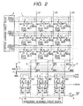
- Fig. 2 is a block diagram of a solid-state image pickup apparatus of a second example useful for understanding the invention.
- a pixel portion 1 in the second.example useful for understanding the invention is constituted by adding to the first example useful for understanding the invention, transfer MOSs M111-M133 for sending the photo-signal charges accumulated in the photodiodes, between the cathode sides of the photodiodes D11-D33 and the gates of the amplification MOSs M311- M333.
- the gate of the transfer MOS M111 is connected to a third row selection line (vertical scanning line) PTX1 arranged so as to extend along the horizontal direction.
- the gates of similar transfer MOSs M121 and M131 in the other pixel cells arranged in the same row are commonly connected to the third row selection line as well.
- the third row selection line is connected to the vertical scanning circuit block 2 similarly to the first and the second row selection lines, and it is supplied with a signal voltage based on an operation timing which is described later.
- the pixel portion other than what is described above is similar to Fig. 1 , and the same reference numerals are assigned to the same construction elements.
- the vertical signal line V1 is connected via a noise-signal transfer switch M11 to a capacitor CTN1 for temporarily holding a noise signal, and is similarly connected via an photo-signal transfer switch M21 to a capacitor CTS1 for temporarily holding an photo-signal. Terminals on the opposite sides of the noise-signal holding capacitor CTN1 and the photo-signal holding capacitor CTS1 are grounded.
- a connecting point of the noise-signal transfer switch M11 and the noise-signal holding capacitor CTN1, and a connecting point of the photo-signal transfer switch M21 and the photo-signal holding capacitor CTS1, are grounded through holding-capacitor reset switches M31 and M32, respectively, and are also connected via horizontal transfer switches M41 and M42 to a differential circuit block 8 for obtaining a difference between the photo-signal and the noise signal.
- the gates of the horizontal transfer switches M41 and M42 are commonly connected to a column selection line H1, and are connected to a horizontal scanning circuit block 7.
- the remaining columns V2 - V3 shown in Fig. 2 are also provided with reading circuits having similar constructions.
- the gates of the noise-signal transfer switches M11 - M13 and the photo-signal transfer switches M21 - M23 connected to each of the columns are commonly connected to PTN and PTS, respectively, and are each provided with signal voltages based on an operation timing described later.
- the PRES1 connected to the gates of the reset MOSs M211 - M231 changes to a high level.
- the gates of the amplification MOSs M311 - M331 are reset to the reset power supply.
- the PSEL1 connected to the gates of the selection MOSs M411 - M431 and the PTN connected to the gates of the noise-signal transfer switches M11 - M13 change to a high level.
- reset signals (noise signals) with the reset noise superimposed thereon are read to the noise-signal holding capacitors CTN1 - CTN3.
- the PTN connected to the gates of the noise-signal transfer switches M11 - M13 returns to a low level.
- the PTX1 connected to the gates of the transfer MOSs M111 - M131 changes to a high level, and the photo-signal charges in the photodiodes D11 - D33 are sent to the gates of the amplification MOSs M311 - M331.
- the PTS connected to the gates of the photo-signal transfer switches M21 - M23 changes to a high level.
- the photo-signals are read out to the photo-signal holding capacitors CTS1 - CTS3.
- the PTS connected to the gates of the photo-signal transfer switches M21 - M23 returns to a low level.
- the noise signals and the photo-signals from the pixel cells connected to the first row are being held in the noise-signal holding capacitors CTN1 - CTN3 and the photo-signal holding capacitors CTS1 - CTS3 which are connected to each of the columns.
- the PRES1 connected to the gates of the reset MOSs M211 - M231 and the PTX1 connected to the gates of the transfer MOSs M111 - M131 change to high level, and the photo-signal charges in the photodiodes D11 - D33 are reset.
- signals H1 - H3 from the horizontal scanning circuit block 7 cause the gates of the horizontal transfer switches M41 - M46 of each column to change to high level sequentially, and the voltages that were being held in the noise-signal holding capacitors CTN1 - CTN3 and the photo-signal holding capacitors CTS1 - CTS3 are read out sequentially to the differential circuit block.
- the differential circuit block the difference between the photo-signals and the noise signals is obtained, and this is outputted sequentially to an output terminal OUT.
- the reading of the pixel cells connected to the first row is completed.
- the PCTR connected to the gates of the reset switches M31 - M36 of the noise-signal holding capacitors CTN1 - CTN3 and the photo-signal holding capacitors CTS1 - CTS3 changes to a high level, and the capacitors are reset by being grounded.
- the subsequent operation is similar, such that the signals of the pixel cells connected to the second and subsequent rows are read out sequentially by means of the signals from the vertical scanning circuit block, and thus the reading of all the pixel cells is completed.
- the drain voltages of the load MOSs M51 - M53 do not change since they are determined by the source voltages of the gate-grounded MOSs M71 - M73. Therefore, even in a case where extremely large signal charges are read out, the electric current values from the load MOSs M51 - M53 can be maintained with little change. Therefore, since neither the number of pixels into which light enters nor the amount of light received cause changes in the voltage drop amount of the GND line 4, the set currents of the load MOSs M51 - M53 are maintained at their fixed levels, regardless of which line is read.
- output voltages of dark pixels are equal between a row which includes pixels into which intense light enters and a row which does not, and thus a problem of a whitish strip occurring in an image upon which a strong spot light is made incident does not occur, whereby enabling a clear image can be obtained.
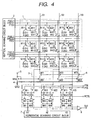
- Fig. 4 is a block diagram of the solid-state image pickup apparatus of a third example useful for understanding the invention.
- the construction of the pixel portion 1 is different from the aforementioned examples.
- the drains of the amplification MOSs M311 - M333 are directly connected to the power supply.
- the source of the amplification MOS M311 is connected via the selection MOS M411 to the vertical signal line V1 arranged so as extend along the vertical direction.
- the sources of similar amplification MOSs M312 and M313 in other pixel cells arranged in the same column are also connected to the vertical signal line V1 via selection MOSs M412 and M413.
- the remaining vertical signal lines V2 - V3 shown in Fig. 4 also have amplification MOSs and selection MOSs connected to them similarly.
- Fig. 5 is a block diagram of the solid-state image pickup apparatus of a fourth example useful for understanding the invention.
- the construction of the constant voltage means 3 is different from the first example useful for understanding the invention, so that in accordance with the present construction, it is not necessary to independently provide the gate voltages of the gate-grounded MOSs M71 - M73 and the gate voltage of the input MOS M50 which sets the constant current for the load.
- Fig. 6 is a block diagram of the solid-state image pickup apparatus of a fifth example useful for understanding the invention.
- the construction of the constant voltage means 3 is different from the first example.
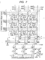
- Fig. 7 is a block diagram of a sixth embodiment of the solid-state image pickup apparatus according 5 to the present invention.
- the pixel portion 1 of the present embodiment has a similar construction to the third example.
- the vertical signal line V1 is connected to a switch M81 for separating the vertical signal line V1 from the load, and to a load MOS M51 serving as a load element, via a gate-grounded MOS M71. Further, the vertical signal line V1 is connected to a clip transistor M310 via a switch M410 for controlling a clip operation.
- the remaining vertical signal lines V2 - V3 shown in Fig. 7 are also connected with amplification MOSs, switches, gate-grounded MOSs, load MOSs, clip transistors and control switches.
- the gates of the switches M81 - M83 and the gates of the gate-grounded MOSs M71 - M73 are commonly connected to a control signal input terminal 9 and to a voltage input terminal 6 for supplying the gate voltage
- the gates of the clip transistors M310 - M330 and the gates of the control switches M410 - M430 are commonly connected to a clip voltage input terminal VCLIP and to a control signal input terminal PSEL, and these gates are respectively supplied with signal voltages based on an operation timing described later.
- the sources of the load MOSs M51 - M53 are connected to a common GND line 4, and the gates thereof are connected to the gate of the input MOS M50 and also connected to the voltage input terminal 5.
- the vertical signal line V1 is connected via a clamp capacitor CO1 and a transfer switch M21 to a capacitor CT1 for temporarily holding the signals, and is connected to an inverting terminal of an operational amplifier 10 in which a feedback capacitor CF and a reset switch MO are connected to a feedback system.
- the noninverting terminal of the operational amplifier 10 is connected to a reference voltage VREF.
- the terminal on the opposite side of the signal holding capacitor CT1 is grounded.
- a junction point of a clamp capacitor CO1 and a transfer switch M21 is connected via a clamp switch M31 to a clamp power source.
- the gate of the horizontal transfer switch M41 is connected to the column selection line H1, and is connected to the horizontal scanning circuit block 7.
- the remaining columns V2 - V3 shown in Fig. 7 are also provided with reading circuits having similar constructions.
- the gates of the clamp switches M31 - M33 connected to each of the columns, and the gates of the transfer switches M21 - M23 are commonly connected to a clamp signal input terminal PCOR and to a transfer signal input terminal PT respectively, and respectively are supplied with signal voltages based on an operation timing which is described later.
- the PTX1 connected to the gates of the transfer MOSs M111 - M131 changes to a high level, and the photo-signal from the photodiodes D11 - D33 are transferred to the gates of the amplification MOSs M311 - M331 and the photo-signals are simultaneously read out by the vertical signal lines V1 - V3.
- the clip transistors M310 - M330 are activated by control signals, so that when the gate voltages of the amplification MOSs M311 - M331 are lower than the clip voltage VCLIP, the voltage of the vertical signal line is clipped by the voltage determined by the clip voltage VCLIP.
- the PT connected to the gates of the transfer MOSs M111 - M131 returns to a low level
- the PT connected to the gates of the transfer switches M21 - M23 changes to a low level. Accordingly, the amount of change from reset signal (the photo-signal) is read out to the signal holding capacitors CT1 - CT3.
- the photo-signals from the pixel cells connected to the first row are held in the signal holding capacitors CT1 - CT3 connected to the columns respectively.
- the PRES1 connected to the gates of the reset MOSs M211 - M231 and the PTX1 connected to the gates of the transfer MOSs M111 - M131 change to high level and the gate control signal 9 for the switches M81 - M83 changes to a low level, and thus the photo-signal charges of the photodiodes D11 - D33 are reset.
- the signals H1 - H3 from the horizontal scanning circuit block cause the gates of the horizontal transfer switches M41 - M46 of each column to change to high level sequentially, and the voltages being held in the signal holding capacitors CT1 - CT3 are read out sequentially to the feedback capacitor CF of the operational amplifier, and are outputted sequentially through an output terminal OUT.
- the electric charge of the feedback capacitor CF is reset by the reset switch MO.
- the reading of the pixel cells connected to the first row is completed.
- the subsequent operation is similar, such that the signals from the pixel cells connected to the second and subsequent rows are read out sequentially due to the signals from the vertical scanning circuit block, and thus the reading of all the pixel cells is completed.
- the drain voltages of the load MOSs M51 - M53 do not change since they are determined by the source voltages of the gate-grounded MOSs M71 - M73. Further, the drain voltages of the gate-grounded MOSs M71 - M73 do not turn off since they are clipped by the clip transistors M310 - M330. Therefore, even in a case where extremely large signal charges are read out, the electric current values of the load MOSs M51 - M53 can be maintained with little change.
- output voltages from dark pixels are equal between a row which includes pixels into which intense light enters and a row which does not, and thus a problem of a whitish strip occurring in an image upon which a strong spot light is made incident does not occur, thereby enabling a clear image to be obtained.
- switches M81 - M83 for separating the vertical signal line V1 from the load, but a similar effect is also produced in a construction in which the voltage 6 that is inputted to the gates of the gate-grounded MOSs M71 - M73 is caused to pulse between the gate-grounded voltage and the ground level.
- Fig. 9 is a block diagram of the solid-state image pickup apparatus of a seventh example useful for understanding the invention.
- the pixel portion 1 is configured as a one-dimensional line sensor.
- the construction of the pixel portion 1 is different from the first example in that there is no selection MOS for selecting the row, and the drains of the amplification MOSs M311 - M331 are directly connected to the power source.
- the photo-signal charges are generated and accumulated and are simultaneously outputted to output lines V4 - V6 of the amplification MOSs M313 - M333.
- the PRES connected to the gates of the reset MOSs M213 - M233 changes to a high level, and the electric charges accumulated in the photodiodes D11 - D33 are reset.
- the output voltages from dark pixels (and from OB pixels) do not change depending on the number of pixels that receive strong light. Therefore, it is not necessary to provide a circuit for clamping the OB at a later stage, and thus the circuitry becomes simple.
- a configuration may be adopted such that a given voltage V6 is applied to the gates of the gate-qrounded MOSs M71 - M73 during the period when the signals from the amplification MOSs inside the pixel cells are being read out by the vertical output lines V1 - V3, and during the other time period, a voltage 6' which is smaller than the voltage 6 is applied to the gates of the gate-grounded MOSs M71 - M73, or the gates of the gate-grounded MOSs M71 - M73 is connected to a ground (GND).
- a constant voltage 6 may be applied during not only the period when the signals are being read out from the amplification MOSs in the pixel cells by the vertical output lines V1 - V3 but also the period when the signals are not being read out.
- the voltages are applied to the gates of the gate-grounded MOSs M71 - M73 only when necessary. Therefore, power consumption is reduced.
- the circuitry has a simple construction.
- the solid-state image pickup apparatus explained in the above first to seventh embodiment and examples may be one which has an OB pixel or one which does not have an OB pixel.
- Fig. 10 is a block diagram of an image pickup system using the solid-state image pickup apparatus according to any one of the first to seventh examples and embodiment explained above.
- Reference numeral 11 denotes the solid-state image pickup apparatus
- reference numeral 12 denotes a programmable gain amp (PGA) for controlling amplitude of output signals from the solid-state image pickup apparatus
- reference numeral 13 denotes an AD converter (ADC)
- reference numeral 14 denotes digital outputs.
- PGA programmable gain amp
- ADC AD converter
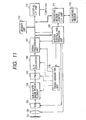
- Fig. 11 is a block diagram showing a case where the solid-state image pickup apparatus according to any one of the above-mentioned first to seventh examples and embodiment is applied in an image pickup system (a still video camera).
- Reference numeral 101 denotes a barrier serving as both a lens protector and a main switch
- reference numeral 102 denotes a lens for imaging an optical image of a photographed object onto a solid-state image pickup element 104
- reference numeral 103 denotes an iris for enabling adjustment of the amount of light passing through the lens 102
- reference numeral 104 denotes the solid-state image pickup apparatus for picking up as an image signal the photographed object imaged by the lens 102
- reference numeral 106 denotes an A/D converter for performing analog/digital conversion of the image signal outputted via an image-pickup-signal processing circuit 105 for performing a gain correction and the like
- reference numeral 107 denotes a signal processing unit for performing various corrections on the image data outputted from the A/D converter
- reference numeral 108 denotes a timing generation unit for outputting various timing signals to the solid-state image pickup element 104, the image-pickup-signal processing circuit 105, the A/D converter 106 and the signal processing unit 107
- reference numeral 109 denotes a system control and operation unit for performing various arithmetic operations and for controlling the still video camera as a whole
- reference numeral 110 denotes a memory unit for temporarily storing the image data
- reference numeral 111 denotes an interface unit for performing recording and reading to/from a recording medium
- reference numeral 112 denotes a removable recording medium such as a semiconductor memory or the like for recording and reading the image data
- reference numeral 113 denotes an interface unit for communicating with an external computer or the like.
- a main power supply turns on, then the power supply for the control system turns on, and also the power supply for the image-pickup system circuitry such as the A/D converter 106 turns on.
- the system control and operation unit 109 opens the iris 103, and after the signal outputted from the solid-state image pickup element 104 is converted by the A/D converter 106, it is inputted to the signal processing unit 107. Based on this data, exposure operation is executed by the control system and operation unit 109.
- Brightness is judged based on a result of a light measurement, and the control system and operation unit 109 controls the iris according to the result of the brightness judgment.
- high-frequency components are extracted based on the signal outputted from the solid-state image pickup element 104, and the control system and operation unit 109 executes an operation to calculate the distance to the photographed object. After that, the lens is driven and a judgment is made whether or not the lens is in focus. If the lens is judged as not in focus, the lens is driven again to measure the distance.
- the main exposure begins.
- the image signal outputted from the solid-state image pickup element 104 undergoes A-D conversion by the A/D converter 106 and then it passes through the signal processing unit 107 to be written to the memory unit by the control system and operation unit 109.
- controls performed by the control system and operation unit 109 cause the data stored in the memory unit 110 to pass through a recording medium control I/F unit to be stored in the semiconductor memory or other such removable recording medium 112.
- the recorded data may also pass through the external I/F 113 and be inputted directly to the computer for image processing.
Claims (3)
- Bildaufnahmevorrichtung mit:einer gemeinsamen Masseleitung (4);einer Vielzahl von Pixeln,wobei jeder Pixel ein fotoelektrisches Umwandlungselement (D11 bis D33) und ein Verstärkungselement (M311 bis M333), das angeordnet ist, ein Signal zu verstärken, das an dem fotoelektrischen Umwandlungselement (D11 bis D33) erzeugt wird, enthält, und wobei die Pixel in einer Pixelanordnung angeordnet sind, die aus Zeilen und Spalten von Pixeln besteht,wobei jede Spalte von Pixeln einer vertikalen Signalleitung (V1 bis V3) und einem Lasttransistor (M51 bis M53) zugeordnet ist; undwobei für jede der Spalten von Pixeln der Lasttransistor (M51 bis M53) angeordnet ist, als eine Last des Verstärkungselements von jedem der Pixel der Spalte zu dienen, und der Lasttransistor einer erste Elektrode, die elektrisch mit der gemeinsamen Masseleitung verbunden ist, und eine zweite Elektrode, die auf einer Seite der vertikalen Signalleitung angeordnet ist, hat; unddadurch gekennzeichnet, dassfür jede der Spalten von Pixeln ein Steuerungstransistor (M71 bis M73) elektrisch zwischen dem Lasttransistor (M51 bis M53) und der vertikalen Signalleitung angeordnet ist, und wobei der Steuerungstransistor (M71 bis M73) angepasst ist, dass an ihn eine gemeinsame konstante Spannung angelegt wird, die allen Spalten gemeinsam ist, um eine Potentialfluktuation der Spannung der zweiten Elektrode des Lasttransistors zu unterdrücken, undjede der Spalten von Pixeln ferner einem jeweiligen Schalter (M81 bis M83) zugeordnet ist, die auf einem elektrischen Pfad angeordnet sind, der den Steuerungstransistor (M71 bis M73), der der jeweiligen Spalte von Pixeln zugeordnet ist, und die vertikale Signalleitung (V1 bis V3), die der jeweiligen Spalte von Pixeln zugeordnet ist, verbindet, wobeifür jede der Spalten von Pixeln eine Seite des Schalters elektrisch mit einer Elektrode des Steuerungstransistors verbunden ist, die auf der Seite der vertikalen Signalleitung des Steuerungstransistors angeordnet ist, und wobei die andere Seite des Schalters elektrisch mit der vertikalen Signalleitung und einer jeweiligen Ausleseschaltung verbunden ist, und wobei der Schalter eine Funktion des Steuerns der elektrischen Verbindung zwischen der vertikalen Signalleitung und dem Steuerungstransistor zumindest für einen Rücksetzbetrieb der Pixel der Spalte und der jeweiligen Ausleseschaltung bevor das Signal, das an dem fotoelektrischen Umwandlungselement (D11 bis D33) an jedem der Pixel der Spalte erzeugt wird, ausgelesen wird, hat.
- Bildaufnahmevorrichtung nach Anspruch 1, die ferner für jede der vertikalen Signalleitungen aufweist:einen Abschneidetransistor (M310 bis M330), der angeordnet ist, die Spannung der vertikalen Signalleitung abzuschneiden.
- Bildaufnahmevorrichtung nach einem der Ansprüche 1 bis 2, die ferner in jedem der Pixel aufweist:einen Transfertransistor (M111 bis M133), der angeordnet ist, ein Signal, das in dem fotoelektrischen Umwandlungselement (D11 bis D33) erzeugt wird, an einen Eingabeabschnitt des Verstärkungselements (M311 bis M333) zu transferieren.
Applications Claiming Priority (2)
| Application Number | Priority Date | Filing Date | Title |
|---|---|---|---|
| JP2001212301A JP3962561B2 (ja) | 2001-07-12 | 2001-07-12 | 固体撮像装置及びそれを用いた撮像システム |
| EP02254791.3A EP1276316B1 (de) | 2001-07-12 | 2002-07-09 | Bildaufnahmevorrichtung |
Related Parent Applications (2)
| Application Number | Title | Priority Date | Filing Date |
|---|---|---|---|
| EP02254791.3 Division | 2002-07-09 | ||
| EP02254791.3A Division EP1276316B1 (de) | 2001-07-12 | 2002-07-09 | Bildaufnahmevorrichtung |
Publications (3)
| Publication Number | Publication Date |
|---|---|
| EP2290953A2 EP2290953A2 (de) | 2011-03-02 |
| EP2290953A3 EP2290953A3 (de) | 2012-04-18 |
| EP2290953B1 true EP2290953B1 (de) | 2015-12-16 |
Family
ID=19047483
Family Applications (3)
| Application Number | Title | Priority Date | Filing Date |
|---|---|---|---|
| EP02254791.3A Expired - Lifetime EP1276316B1 (de) | 2001-07-12 | 2002-07-09 | Bildaufnahmevorrichtung |
| EP12167310.7A Withdrawn EP2493177A3 (de) | 2001-07-12 | 2002-07-09 | Bildaufnahmevorrichtung |
| EP10182083.5A Expired - Lifetime EP2290953B1 (de) | 2001-07-12 | 2002-07-09 | Bildaufnahmevorrichtung |
Family Applications Before (2)
| Application Number | Title | Priority Date | Filing Date |
|---|---|---|---|
| EP02254791.3A Expired - Lifetime EP1276316B1 (de) | 2001-07-12 | 2002-07-09 | Bildaufnahmevorrichtung |
| EP12167310.7A Withdrawn EP2493177A3 (de) | 2001-07-12 | 2002-07-09 | Bildaufnahmevorrichtung |
Country Status (6)
| Country | Link |
|---|---|
| US (4) | US7355645B2 (de) |
| EP (3) | EP1276316B1 (de) |
| JP (1) | JP3962561B2 (de) |
| KR (1) | KR100498222B1 (de) |
| CN (1) | CN1222046C (de) |
| TW (1) | TW554546B (de) |
Families Citing this family (27)
| Publication number | Priority date | Publication date | Assignee | Title |
|---|---|---|---|---|
| JP3685445B2 (ja) * | 2000-02-18 | 2005-08-17 | キヤノン株式会社 | 固体撮像装置及び撮像システム |
| JP3962561B2 (ja) | 2001-07-12 | 2007-08-22 | キヤノン株式会社 | 固体撮像装置及びそれを用いた撮像システム |
| US7408577B2 (en) * | 2003-04-09 | 2008-08-05 | Micron Technology, Inc. | Biasing scheme for large format CMOS active pixel sensors |
| US7446806B2 (en) * | 2003-12-19 | 2008-11-04 | Symbol Technologies, Inc. | Single chip, noise-resistant, one-dimensional, CMOS sensor for target imaging |
| JP4279880B2 (ja) * | 2004-07-06 | 2009-06-17 | パナソニック株式会社 | 固体撮像装置 |
| JP5247007B2 (ja) | 2005-06-09 | 2013-07-24 | キヤノン株式会社 | 撮像装置及び撮像システム |
| JP5340374B2 (ja) * | 2005-06-09 | 2013-11-13 | キヤノン株式会社 | 撮像装置及び撮像システム |
| US8081837B2 (en) * | 2006-02-07 | 2011-12-20 | Intel Corporation | Image sensor array leakage and dark current compensation |
| JP4416753B2 (ja) * | 2006-03-31 | 2010-02-17 | キヤノン株式会社 | 固体撮像装置 |
| JP4193874B2 (ja) * | 2006-05-25 | 2008-12-10 | ソニー株式会社 | 固体撮像装置とその製造方法、及びカメラモジュール |
| JP4185949B2 (ja) * | 2006-08-08 | 2008-11-26 | キヤノン株式会社 | 光電変換装置及び撮像装置 |
| JP4952301B2 (ja) * | 2007-03-01 | 2012-06-13 | ソニー株式会社 | 撮像装置およびカメラ |
| JP5105907B2 (ja) * | 2007-03-06 | 2012-12-26 | キヤノン株式会社 | 撮像システム |
| JP4065979B1 (ja) * | 2007-06-18 | 2008-03-26 | キヤノン株式会社 | 撮像システム、撮像センサ、及び撮像システムの制御方法 |
| JP4931233B2 (ja) | 2007-07-04 | 2012-05-16 | キヤノン株式会社 | 撮像装置及びその処理方法 |
| JP5106092B2 (ja) | 2007-12-26 | 2012-12-26 | パナソニック株式会社 | 固体撮像装置およびカメラ |
| JP5371463B2 (ja) | 2008-02-28 | 2013-12-18 | キヤノン株式会社 | 撮像装置、撮像システム、および、撮像装置の制御方法 |
| JP2010183462A (ja) * | 2009-02-06 | 2010-08-19 | Panasonic Corp | 固体撮像装置及びカメラ |
| JP5282690B2 (ja) * | 2009-07-23 | 2013-09-04 | ソニー株式会社 | 画素回路、固体撮像素子、およびカメラシステム |
| JP5481230B2 (ja) * | 2010-02-26 | 2014-04-23 | パナソニック株式会社 | 撮像装置及び固体撮像装置 |
| JP5856392B2 (ja) | 2011-06-06 | 2016-02-09 | キヤノン株式会社 | 固体撮像装置およびカメラ |
| US8814449B2 (en) * | 2011-07-22 | 2014-08-26 | Nikon Corporation | Adapter, camera system, and adapter control program |
| JP5990080B2 (ja) * | 2012-10-05 | 2016-09-07 | キヤノン株式会社 | 撮像システム、および撮像システムの駆動方法 |
| WO2014129118A1 (ja) | 2013-02-21 | 2014-08-28 | パナソニック株式会社 | 固体撮像装置 |
| TWI497998B (zh) * | 2013-03-13 | 2015-08-21 | Himax Imaging Ltd | 影像感測器 |
| JP6174901B2 (ja) | 2013-05-10 | 2017-08-02 | キヤノン株式会社 | 固体撮像装置及びカメラ |
| JP6674219B2 (ja) * | 2015-10-01 | 2020-04-01 | キヤノン株式会社 | 固体撮像装置及び撮像システム |
Family Cites Families (23)
| Publication number | Priority date | Publication date | Assignee | Title |
|---|---|---|---|---|
| DE3539875A1 (de) | 1985-11-11 | 1987-05-14 | Keller & Bohacek Gmbh | Verfahren und vorrichtung zum herstellen enzymhaltiger biomasse aus zuckerruebenschnitzeln |
| US5144447A (en) * | 1988-03-31 | 1992-09-01 | Hitachi, Ltd. | Solid-state image array with simultaneously activated line drivers |
| JPH04342305A (ja) | 1991-05-20 | 1992-11-27 | Matsushita Electric Ind Co Ltd | 利得制御回路 |
| US5406332A (en) * | 1992-03-06 | 1995-04-11 | Canon Kabushiki Kaisha | Photoelectric converting device |
| JP2989992B2 (ja) * | 1993-05-19 | 1999-12-13 | 松下電器産業株式会社 | イメージセンサ |
| JP3031606B2 (ja) * | 1995-08-02 | 2000-04-10 | キヤノン株式会社 | 固体撮像装置と画像撮像装置 |
| JP3845449B2 (ja) * | 1995-08-11 | 2006-11-15 | 株式会社東芝 | Mos型固体撮像装置 |
| JP3474700B2 (ja) * | 1996-03-13 | 2003-12-08 | 株式会社東芝 | 固体撮像装置 |
| US5680038A (en) * | 1996-06-20 | 1997-10-21 | Lsi Logic Corporation | High-swing cascode current mirror |
| JPH10257389A (ja) * | 1997-03-11 | 1998-09-25 | Toshiba Corp | 増幅型固体撮像装置及びその動作方法 |
| JP3466886B2 (ja) * | 1997-10-06 | 2003-11-17 | キヤノン株式会社 | 固体撮像装置 |
| US5966005A (en) * | 1997-12-18 | 1999-10-12 | Asahi Corporation | Low voltage self cascode current mirror |
| US6963372B1 (en) | 1998-04-24 | 2005-11-08 | Canon Kabushiki Kaisha | Solid-state image sensing apparatus and method of operating the same |
| JP4083909B2 (ja) * | 1998-06-02 | 2008-04-30 | 株式会社東芝 | 固体撮像装置 |
| KR100352757B1 (ko) * | 1998-06-02 | 2002-09-16 | 가부시끼가이샤 도시바 | 고속도 동작 고체 촬상 장치 |
| JP4192305B2 (ja) | 1998-08-27 | 2008-12-10 | 株式会社ニコン | 固体撮像素子 |
| US6731397B1 (en) * | 1999-05-21 | 2004-05-04 | Foveon, Inc. | Method for storing and retrieving digital image data from an imaging array |
| JP3693281B2 (ja) * | 1999-09-30 | 2005-09-07 | シャープ株式会社 | 増幅型固体撮像装置 |
| US6727946B1 (en) * | 1999-12-14 | 2004-04-27 | Omnivision Technologies, Inc. | APS soft reset circuit for reducing image lag |
| JP3685445B2 (ja) * | 2000-02-18 | 2005-08-17 | キヤノン株式会社 | 固体撮像装置及び撮像システム |
| JP3667186B2 (ja) * | 2000-02-29 | 2005-07-06 | キヤノン株式会社 | 信号転送装置及びそれを用いた固体撮像装置 |
| KR100397663B1 (ko) * | 2000-06-23 | 2003-09-13 | (주) 픽셀플러스 | 데이터 입출력선이 리셋 모드의 전압으로 유지되는 씨모스 이미지 센서 |
| JP3962561B2 (ja) | 2001-07-12 | 2007-08-22 | キヤノン株式会社 | 固体撮像装置及びそれを用いた撮像システム |
-
2001
- 2001-07-12 JP JP2001212301A patent/JP3962561B2/ja not_active Expired - Fee Related
-
2002
- 2002-07-09 EP EP02254791.3A patent/EP1276316B1/de not_active Expired - Lifetime
- 2002-07-09 US US10/190,713 patent/US7355645B2/en active Active
- 2002-07-09 EP EP12167310.7A patent/EP2493177A3/de not_active Withdrawn
- 2002-07-09 EP EP10182083.5A patent/EP2290953B1/de not_active Expired - Lifetime
- 2002-07-11 CN CNB021406502A patent/CN1222046C/zh not_active Expired - Fee Related
- 2002-07-12 KR KR10-2002-0040556A patent/KR100498222B1/ko active IP Right Grant
- 2002-07-12 TW TW091115582A patent/TW554546B/zh not_active IP Right Cessation
-
2007
- 2007-09-26 US US11/861,790 patent/US7986362B2/en not_active Expired - Fee Related
-
2011
- 2011-06-13 US US13/158,613 patent/US8553120B2/en not_active Expired - Lifetime
-
2013
- 2013-09-03 US US14/016,344 patent/US9055211B2/en not_active Expired - Fee Related
Also Published As
| Publication number | Publication date |
|---|---|
| JP2003032548A (ja) | 2003-01-31 |
| EP2493177A3 (de) | 2013-11-13 |
| CN1398105A (zh) | 2003-02-19 |
| US9055211B2 (en) | 2015-06-09 |
| EP1276316B1 (de) | 2013-06-12 |
| US20140002689A1 (en) | 2014-01-02 |
| EP2290953A3 (de) | 2012-04-18 |
| US8553120B2 (en) | 2013-10-08 |
| US7355645B2 (en) | 2008-04-08 |
| EP2290953A2 (de) | 2011-03-02 |
| US7986362B2 (en) | 2011-07-26 |
| TW554546B (en) | 2003-09-21 |
| KR100498222B1 (ko) | 2005-06-29 |
| US20030011831A1 (en) | 2003-01-16 |
| US20110242382A1 (en) | 2011-10-06 |
| EP2493177A2 (de) | 2012-08-29 |
| KR20030007139A (ko) | 2003-01-23 |
| EP1276316A2 (de) | 2003-01-15 |
| JP3962561B2 (ja) | 2007-08-22 |
| CN1222046C (zh) | 2005-10-05 |
| EP1276316A3 (de) | 2009-09-02 |
| US20080012976A1 (en) | 2008-01-17 |
Similar Documents
| Publication | Publication Date | Title |
|---|---|---|
| EP2290953B1 (de) | Bildaufnahmevorrichtung | |
| US7812876B2 (en) | Photoelectric conversion device and image capturing device with variable amplifier for amplifying signal by a selected gain | |
| JP3685445B2 (ja) | 固体撮像装置及び撮像システム | |
| US8427558B2 (en) | Image pickup apparatus | |
| US7561199B2 (en) | Solid-state image pickup device | |
| US7903150B2 (en) | Differential amplifier circuit used in solid-state image pickup apparatus, and arrangement that avoids influence of variations of integrated circuits in manufacture and the like | |
| US8330843B2 (en) | Solid-state image sensing device, method for driving solid-state image sensing device, and image sensing system incorporated with solid-state image sensing device | |
| JP4315032B2 (ja) | 固体撮像装置および固体撮像装置の駆動方法 | |
| EP1326428A2 (de) | Bildaufnahmevorrichtung | |
| JP2007158626A (ja) | 固体撮像装置 | |
| US20050253946A1 (en) | Solid-state image pickup device and camera utilizing the same | |
| JP2008124527A (ja) | 固体撮像装置及び撮像装置 | |
| JP3870137B2 (ja) | 固体撮像装置及び固体撮像システム | |
| US9426391B2 (en) | Solid-state imaging apparatus, method of controlling the same, and imaging system | |
| TWI760285B (zh) | 影像感測器的畫素單元、成像系統及讀取影像信號的方法 | |
| JP2005348041A (ja) | 固体撮像装置および撮像システム | |
| JP2007143067A (ja) | 撮像装置及び撮像システム | |
| US20040223064A1 (en) | Image pickup element, image pickup device, and differential amplifying circuit | |
| JP2007214791A (ja) | 撮像素子、撮像装置、及び撮像素子の駆動方法 |
Legal Events
| Date | Code | Title | Description |
|---|---|---|---|
| PUAI | Public reference made under article 153(3) epc to a published international application that has entered the european phase |
Free format text: ORIGINAL CODE: 0009012 |
|
| AC | Divisional application: reference to earlier application |
Ref document number: 1276316 Country of ref document: EP Kind code of ref document: P |
|
| AK | Designated contracting states |
Kind code of ref document: A2 Designated state(s): DE FR GB IT NL |
|
| PUAL | Search report despatched |
Free format text: ORIGINAL CODE: 0009013 |
|
| AK | Designated contracting states |
Kind code of ref document: A3 Designated state(s): DE FR GB IT NL |
|
| RIC1 | Information provided on ipc code assigned before grant |
Ipc: H04N 5/335 20110101AFI20120309BHEP |
|
| 17P | Request for examination filed |
Effective date: 20121018 |
|
| 17Q | First examination report despatched |
Effective date: 20140704 |
|
| GRAP | Despatch of communication of intention to grant a patent |
Free format text: ORIGINAL CODE: EPIDOSNIGR1 |
|
| INTG | Intention to grant announced |
Effective date: 20150626 |
|
| GRAS | Grant fee paid |
Free format text: ORIGINAL CODE: EPIDOSNIGR3 |
|
| GRAA | (expected) grant |
Free format text: ORIGINAL CODE: 0009210 |
|
| AC | Divisional application: reference to earlier application |
Ref document number: 1276316 Country of ref document: EP Kind code of ref document: P |
|
| AK | Designated contracting states |
Kind code of ref document: B1 Designated state(s): DE FR GB IT NL |
|
| REG | Reference to a national code |
Ref country code: GB Ref legal event code: FG4D |
|
| REG | Reference to a national code |
Ref country code: DE Ref legal event code: R096 Ref document number: 60247677 Country of ref document: DE |
|
| REG | Reference to a national code |
Ref country code: NL Ref legal event code: MP Effective date: 20151216 |
|
| PG25 | Lapsed in a contracting state [announced via postgrant information from national office to epo] |
Ref country code: NL Free format text: LAPSE BECAUSE OF FAILURE TO SUBMIT A TRANSLATION OF THE DESCRIPTION OR TO PAY THE FEE WITHIN THE PRESCRIBED TIME-LIMIT Effective date: 20151216 |
|
| PG25 | Lapsed in a contracting state [announced via postgrant information from national office to epo] |
Ref country code: IT Free format text: LAPSE BECAUSE OF FAILURE TO SUBMIT A TRANSLATION OF THE DESCRIPTION OR TO PAY THE FEE WITHIN THE PRESCRIBED TIME-LIMIT Effective date: 20151216 |
|
| REG | Reference to a national code |
Ref country code: DE Ref legal event code: R097 Ref document number: 60247677 Country of ref document: DE |
|
| PLBE | No opposition filed within time limit |
Free format text: ORIGINAL CODE: 0009261 |
|
| STAA | Information on the status of an ep patent application or granted ep patent |
Free format text: STATUS: NO OPPOSITION FILED WITHIN TIME LIMIT |
|
| 26N | No opposition filed |
Effective date: 20160919 |
|
| GBPC | Gb: european patent ceased through non-payment of renewal fee |
Effective date: 20160709 |
|
| PG25 | Lapsed in a contracting state [announced via postgrant information from national office to epo] |
Ref country code: FR Free format text: LAPSE BECAUSE OF NON-PAYMENT OF DUE FEES Effective date: 20160801 |
|
| REG | Reference to a national code |
Ref country code: FR Ref legal event code: ST Effective date: 20170331 |
|
| PG25 | Lapsed in a contracting state [announced via postgrant information from national office to epo] |
Ref country code: GB Free format text: LAPSE BECAUSE OF NON-PAYMENT OF DUE FEES Effective date: 20160709 |
|
| PGFP | Annual fee paid to national office [announced via postgrant information from national office to epo] |
Ref country code: DE Payment date: 20180928 Year of fee payment: 17 |
|
| REG | Reference to a national code |
Ref country code: DE Ref legal event code: R119 Ref document number: 60247677 Country of ref document: DE |
|
| PG25 | Lapsed in a contracting state [announced via postgrant information from national office to epo] |
Ref country code: DE Free format text: LAPSE BECAUSE OF NON-PAYMENT OF DUE FEES Effective date: 20200201 |