EP2290753A1 - Steckverbinder und Multilayerplatine - Google Patents
Steckverbinder und Multilayerplatine Download PDFInfo
- Publication number
- EP2290753A1 EP2290753A1 EP09011143A EP09011143A EP2290753A1 EP 2290753 A1 EP2290753 A1 EP 2290753A1 EP 09011143 A EP09011143 A EP 09011143A EP 09011143 A EP09011143 A EP 09011143A EP 2290753 A1 EP2290753 A1 EP 2290753A1
- Authority
- EP
- European Patent Office
- Prior art keywords
- multilayer board
- connector
- contacting
- contact elements
- contact element
- Prior art date
- Legal status (The legal status is an assumption and is not a legal conclusion. Google has not performed a legal analysis and makes no representation as to the accuracy of the status listed.)
- Granted
Links
Images



Classifications
-
- H—ELECTRICITY
- H01—ELECTRIC ELEMENTS
- H01R—ELECTRICALLY-CONDUCTIVE CONNECTIONS; STRUCTURAL ASSOCIATIONS OF A PLURALITY OF MUTUALLY-INSULATED ELECTRICAL CONNECTING ELEMENTS; COUPLING DEVICES; CURRENT COLLECTORS
- H01R12/00—Structural associations of a plurality of mutually-insulated electrical connecting elements, specially adapted for printed circuits, e.g. printed circuit boards [PCB], flat or ribbon cables, or like generally planar structures, e.g. terminal strips, terminal blocks; Coupling devices specially adapted for printed circuits, flat or ribbon cables, or like generally planar structures; Terminals specially adapted for contact with, or insertion into, printed circuits, flat or ribbon cables, or like generally planar structures
- H01R12/70—Coupling devices
- H01R12/71—Coupling devices for rigid printing circuits or like structures
- H01R12/72—Coupling devices for rigid printing circuits or like structures coupling with the edge of the rigid printed circuits or like structures
- H01R12/722—Coupling devices for rigid printing circuits or like structures coupling with the edge of the rigid printed circuits or like structures coupling devices mounted on the edge of the printed circuits
- H01R12/727—Coupling devices presenting arrays of contacts
-
- H—ELECTRICITY
- H01—ELECTRIC ELEMENTS
- H01R—ELECTRICALLY-CONDUCTIVE CONNECTIONS; STRUCTURAL ASSOCIATIONS OF A PLURALITY OF MUTUALLY-INSULATED ELECTRICAL CONNECTING ELEMENTS; COUPLING DEVICES; CURRENT COLLECTORS
- H01R12/00—Structural associations of a plurality of mutually-insulated electrical connecting elements, specially adapted for printed circuits, e.g. printed circuit boards [PCB], flat or ribbon cables, or like generally planar structures, e.g. terminal strips, terminal blocks; Coupling devices specially adapted for printed circuits, flat or ribbon cables, or like generally planar structures; Terminals specially adapted for contact with, or insertion into, printed circuits, flat or ribbon cables, or like generally planar structures
-
- H—ELECTRICITY
- H05—ELECTRIC TECHNIQUES NOT OTHERWISE PROVIDED FOR
- H05K—PRINTED CIRCUITS; CASINGS OR CONSTRUCTIONAL DETAILS OF ELECTRIC APPARATUS; MANUFACTURE OF ASSEMBLAGES OF ELECTRICAL COMPONENTS
- H05K1/00—Printed circuits
- H05K1/02—Details
- H05K1/11—Printed elements for providing electric connections to or between printed circuits
- H05K1/111—Pads for surface mounting, e.g. lay-out
- H05K1/112—Pads for surface mounting, e.g. lay-out directly combined with via connections
-
- H—ELECTRICITY
- H05—ELECTRIC TECHNIQUES NOT OTHERWISE PROVIDED FOR
- H05K—PRINTED CIRCUITS; CASINGS OR CONSTRUCTIONAL DETAILS OF ELECTRIC APPARATUS; MANUFACTURE OF ASSEMBLAGES OF ELECTRICAL COMPONENTS
- H05K3/00—Apparatus or processes for manufacturing printed circuits
- H05K3/30—Assembling printed circuits with electric components, e.g. with resistors
- H05K3/306—Assembling printed circuits with electric components, e.g. with resistors with lead-in-hole components
- H05K3/308—Adaptations of leads
-
- H—ELECTRICITY
- H01—ELECTRIC ELEMENTS
- H01R—ELECTRICALLY-CONDUCTIVE CONNECTIONS; STRUCTURAL ASSOCIATIONS OF A PLURALITY OF MUTUALLY-INSULATED ELECTRICAL CONNECTING ELEMENTS; COUPLING DEVICES; CURRENT COLLECTORS
- H01R13/00—Details of coupling devices of the kinds covered by groups H01R12/70 or H01R24/00 - H01R33/00
- H01R13/648—Protective earth or shield arrangements on coupling devices, e.g. anti-static shielding
- H01R13/658—High frequency shielding arrangements, e.g. against EMI [Electro-Magnetic Interference] or EMP [Electro-Magnetic Pulse]
-
- H—ELECTRICITY
- H05—ELECTRIC TECHNIQUES NOT OTHERWISE PROVIDED FOR
- H05K—PRINTED CIRCUITS; CASINGS OR CONSTRUCTIONAL DETAILS OF ELECTRIC APPARATUS; MANUFACTURE OF ASSEMBLAGES OF ELECTRICAL COMPONENTS
- H05K1/00—Printed circuits
- H05K1/02—Details
- H05K1/0296—Conductive pattern lay-out details not covered by sub groups H05K1/02 - H05K1/0295
- H05K1/0298—Multilayer circuits
-
- H—ELECTRICITY
- H05—ELECTRIC TECHNIQUES NOT OTHERWISE PROVIDED FOR
- H05K—PRINTED CIRCUITS; CASINGS OR CONSTRUCTIONAL DETAILS OF ELECTRIC APPARATUS; MANUFACTURE OF ASSEMBLAGES OF ELECTRICAL COMPONENTS
- H05K2201/00—Indexing scheme relating to printed circuits covered by H05K1/00
- H05K2201/09—Shape and layout
- H05K2201/09209—Shape and layout details of conductors
- H05K2201/09372—Pads and lands
- H05K2201/094—Array of pads or lands differing from one another, e.g. in size, pitch or thickness; Using different connections on the pads
-
- H—ELECTRICITY
- H05—ELECTRIC TECHNIQUES NOT OTHERWISE PROVIDED FOR
- H05K—PRINTED CIRCUITS; CASINGS OR CONSTRUCTIONAL DETAILS OF ELECTRIC APPARATUS; MANUFACTURE OF ASSEMBLAGES OF ELECTRICAL COMPONENTS
- H05K2201/00—Indexing scheme relating to printed circuits covered by H05K1/00
- H05K2201/09—Shape and layout
- H05K2201/09209—Shape and layout details of conductors
- H05K2201/09372—Pads and lands
- H05K2201/09472—Recessed pad for surface mounting; Recessed electrode of component
-
- H—ELECTRICITY
- H05—ELECTRIC TECHNIQUES NOT OTHERWISE PROVIDED FOR
- H05K—PRINTED CIRCUITS; CASINGS OR CONSTRUCTIONAL DETAILS OF ELECTRIC APPARATUS; MANUFACTURE OF ASSEMBLAGES OF ELECTRICAL COMPONENTS
- H05K2201/00—Indexing scheme relating to printed circuits covered by H05K1/00
- H05K2201/09—Shape and layout
- H05K2201/09209—Shape and layout details of conductors
- H05K2201/095—Conductive through-holes or vias
- H05K2201/09509—Blind vias, i.e. vias having one side closed
-
- H—ELECTRICITY
- H05—ELECTRIC TECHNIQUES NOT OTHERWISE PROVIDED FOR
- H05K—PRINTED CIRCUITS; CASINGS OR CONSTRUCTIONAL DETAILS OF ELECTRIC APPARATUS; MANUFACTURE OF ASSEMBLAGES OF ELECTRICAL COMPONENTS
- H05K2201/00—Indexing scheme relating to printed circuits covered by H05K1/00
- H05K2201/10—Details of components or other objects attached to or integrated in a printed circuit board
- H05K2201/10007—Types of components
- H05K2201/10189—Non-printed connector
-
- H—ELECTRICITY
- H05—ELECTRIC TECHNIQUES NOT OTHERWISE PROVIDED FOR
- H05K—PRINTED CIRCUITS; CASINGS OR CONSTRUCTIONAL DETAILS OF ELECTRIC APPARATUS; MANUFACTURE OF ASSEMBLAGES OF ELECTRICAL COMPONENTS
- H05K3/00—Apparatus or processes for manufacturing printed circuits
- H05K3/30—Assembling printed circuits with electric components, e.g. with resistors
- H05K3/32—Assembling printed circuits with electric components, e.g. with resistors electrically connecting electric components or wires to printed circuits
- H05K3/34—Assembling printed circuits with electric components, e.g. with resistors electrically connecting electric components or wires to printed circuits by soldering
- H05K3/341—Surface mounted components
- H05K3/3421—Leaded components
- H05K3/3426—Leaded components characterised by the leads
Definitions
- the invention relates to a multi-pin connector for contacting with a multilayer board, of a multilayer board for assembly with a multi-pin connector and a combination of a multi-pin connector and a provided for mounting the connector multilayer board.
- test holes in which the exact depth of the respective interconnect layer is determined by detecting a current flow as soon as the drill bit reaches the interconnect layer. The detection of consecutively lying in the drilling direction interconnect layers is thereby reliably possible that are used from one conductor layer to conductor layer each drills with a smaller bore diameter, so Short circuits between different interconnect layers are avoided.
- the publication DE 199 02 950 A1 describes the production of a printed circuit board that can be fitted with connectors from both sides.
- the circuit board is composed of two multilayer printed circuit boards, which are glued together.
- the two printed circuit boards contain a large number of plated-through holes, which are connected to each other by the tracks of the multilayer board.
- the plated-through holes are provided for receiving the terminal pins of the connector.
- the connection pins are pressed into the holes, whereby the electrical and mechanical connection to the holes is to be made.
- the in the utility model DE 296 01 655 U1 described printed circuit board which is also provided for double-sided contacting with connectors, is also made of two glued together multilayer printed circuit boards.
- the connection pins of the connectors are pressed into the holes, which can be realized as blind holes.
- the in the published patent application DE 40 02 025 A1 described multilayer board contains through holes in the form of continuously conductive coated walls of holes, which have contact points with selected interconnect layers of the multilayer board.
- the plated-through holes have a region with a raised cross-section at the upper end.
- the raised cross-section is formed in at least one separate laminated cover plate.
- the areas with the increased cross-section are provided for receiving connector pins of connectors.
- Some of the holes may also be blind to avoid being shorted to interconnect layers below them.
- each signal leading contact element is associated with a screening or ground potential leading contact element.
- the orientation of the contact elements is made such that an impedance matching is made possible.
- the invention has for its object to provide a multi-pin connector for contacting with a multilayer board, a multilayer board for assembly with a multi-pin connector and a combination of a multi-pin connector and a to provide each equipped with the multipolar connector provided multilayer board, which allow a management of signals with very high frequencies, in particular of digital signals.
- the multi-pin connector for contacting with a multilayer board is based on a large number of contact elements.
- the connector according to the invention is characterized in that the connection pins of the contact elements are of different lengths for contacting the connection pins with provided in different interconnect levels interconnects of the multilayer board.
- blind holes are provided for contacting terminal pins of the contact elements of the multi-pin connector.
- the multilayer printed circuit board according to the invention is characterized in that the blind bores terminate in different interconnect levels of the multilayer board for targeted contacting of the terminal pins of the contact elements with interconnects of the multilayer board provided in the different interconnect levels.
- the multi-pin connector for contacting the multilayer board has a plurality of contact elements and that the multilayer board for mounting with the multi-pin connector blind holes for contacting terminal pins of the contact elements of the multi-pin connector having.
- the inventive combination of a multi-pin connector and adapted for assembly with the multi-pin connector multilayer board is characterized in that the terminal pins of the contact elements of the connector are different lengths for contacting the terminal pins provided in different interconnects interconnects of the multilayer board and that the Blind holes in different interconnect levels of the multilayer board for targeted contacting of the length-matched terminal pins of the contact elements end.
- the multi-pin connector according to the invention, the multilayer board according to the invention and the inventive combination of the multi-pin connector and the multilayer board initially allow a high density of contact elements of the connector. This is achieved by a correspondingly high density of interconnects in the multilayer board, which are available for contacting with the connection pins of the contact elements of the connector.
- the conductor paths of the multilayer board guided in the different conductor track planes can now have a simple geometric design.
- all traces can be led away in a straight line without evasive curves of the terminal pins of the contact elements of the connector.
- the multi-pin connector according to the invention, the multilayer board according to the invention and the inventive combination of the multi-pin connector and the multilayer board for very high frequencies of the contact elements of the connector to leading signals which can be up to 40 GigaBit / s in digital signals, without that the attenuation becomes too large or the eye pattern of the digital signals collapses.
- the multi-pin connector according to the invention, the multilayer board according to the invention and the inventive combination of the multi-pin connector and the multilayer board are particularly suitable in an application in which the multilayer board is used as a backplane or in which the multilayer board for contacting with a backplane.
- this technology realizes devices of the telecommunications industry, which process high-frequency digital signals, for example, for signal transmissions of the Internet.
- An embodiment of the multipolar connector according to the invention provides that those terminal pins of the connector, which are arranged in the assembled state with the multilayer board closer to the edge of the multilayer board, are the longest and behind each end in stages less long. Accordingly, a corresponding embodiment of the multilayer board according to the invention provides that the blind bores are at the edge of the multilayer board at the lowest and behind each end in stages less deep. With these measures, a compensation of the resulting line lengths of stacked contact element rows of the connector can be approximated by the fact that arranged at the lower end of the connector contact elements may have longer connection pins than the connection pins of the contact elements of the above arranged in the connector contact element rows, if is assumed by a multi-pole angle connector.
- a particularly advantageous measure provides that the connection pins of signal-carrying contact element pairs of multi-pin connector, which are arranged side by side in a contact element row of the connector, each having the same length. Accordingly, a corresponding particularly advantageous measure provides that the blind holes in the multilayer board, which end for contacting with connection pins of contact element pairs, which are arranged in a row of contact elements of the connector side by side, each end equally deep in the multilayer board. With these measures, the electrical properties of both the multi-pin connector and the multilayer board in the area provided for contacting with the terminal pins of the connector traces can be tailored to the guided by the signal contact element pair signals. As a result, these measures have a particularly advantageous effect if the corresponding contact element pairs carry differential signals between which no signal propagation time differences should occur.
- the described measure is provided for all lying in a row of contact elements contact elements of the connector. Accordingly, the measure corresponding thereto is preferably provided for the blind holes in the multilayer board, which are provided for contacting the terminal pins of a lying in a contact element row contact elements of the connector. As a result, identical electrical properties are provided for a plurality of pairs of contact elements, which preferably carry differential signals.
- connection pins fill the depth of the respective blind holes associated with the connection pins at least approximately completely.
- the contact element pairs of the connector and / or that the contact element pairs associated conductor tracks of the multilayer board are each realized at least approximately with a predetermined characteristic impedance.
- the multilayer board 11 may have conductor tracks, not shown in greater detail, which run in different conductor track planes. Due to bores 15a, 15b bored through the multilayer board 11 in each case for example, the bends 20a, 20b of the printed conductors 17a, 17b are required in the interconnects arranged in possibly different printed circuit traces FIG. 2 are shown.
- FIG. 5 shown isometric view of a plurality of contact elements 50a, 50b - 50'a, 50'b of a multi-pole, contacted with a multilayer board 51 connector according to the invention
- the tracks 52a, 52b of the contact elements 50a, 50b shown in a straight line without bends from the in FIG. 5 invisible connecting pins 53a, 53b of the contact elements 50a, 50b are carried away on the uppermost interconnect level 54 of the multilayer board 51, wherein the uppermost interconnect level 54 also exemplarily corresponds to the surface of the multilayer board 51 according to the invention.
- the contact elements 50a, 50b - 50'a, 50'b are arranged in pairs in each contact row direction 13, wherein in the embodiment shown, six pairs of contact elements in contact row direction 13 and eight contact element pairs are arranged in the contact column direction 12.
- FIG. 5 shown parts that correspond to the parts shown in the preceding figures, each bear the same reference numerals. The same agreement applies mutatis mutandis, in particular for the following figures.
- top view of the top conductor track plane 54 of the multilayer board 51 illustrates the running in a straight line guide the tracks 52a, 52b of the holes 60a, 60b leading traces 52a, 52b, in which the connection pins 53a, 53b of the contact elements 50a, 50b are anchored in each case.
- FIG. 7 clearly showing an isometric view of a section through the multilayer board 51 according to the invention.
- conductor tracks 52a, 52b on the surface of the multilayer board 51 are now exemplary conductor tracks 72a, 72b - 72'a, 72'b (see also FIG. 12 ) may be provided, which lie within the multilayer board 51 in different Leitbahnebenen 71 - 71 '.
- the bores 60a-60'a in the multilayer board 51 are designed as blind bores, with the printed conductors 72a, 72b-72'a, 72'b guided in the different printed circuit layers 71-71 'leading to the individual blind bores 60a, 60b-60'a , 60'b are guided.
- FIG. 7 Due to the cut, only the printed conductors 72a-72b and the blind holes 60a-60'a can be seen.
- connection pins 53a, 53b-53'a, 53'b of the contact elements 50a, 50b-50'a, 50'b are to be matched to the blind holes 60a, 60b-60'a, 60'b such that the Connection pins 53a, 53b - 53'a, 53'b maximum length of the associated blind holes 60a, 60b - have 60'a, 60'b.
- FIG. 8 making a cut through the in FIG. 7 illustrates illustrated the blind holes 60a, 60b - 60'a, 60'b, wherein due to the cut, only the blind holes 60a - 60'a can be seen, which end in different conductor tracks 71 - 71 ', in each of which the printed conductors 72a, 72b - 72'a, 72'b are accommodated, of which the printed conductors 72a - 72'a can be seen.
- the interconnects 72a, 72b-72'a, 72'b respectively provide the connections to those in the blind bores 60a, 60b-60'a, 60'b, in FIG FIG.
- connection pins 53a, 53b - 53'a, 53'b of the contact elements 50a, 50b - 50'a, 50'b ago wherein in the blind holes 60a, 60b - 60'a, 60'b, for example, metallizations are present , which enable the electrical contact with the connection pins 53a, 53b-53'a, 53'b to be soldered or preferably to be pressed.
- FIGS. 7 and 8 show the advantageous embodiment of the paired arrangement of contact elements 50a, 50b - 50'a, 50'b, wherein a pair of contact elements 50a, 50b - 50'a, 50'b preferably leads differential signals.
- a pair of contact elements 50a, 50b - 50'a, 50'b preferably leads differential signals.
- the two contact elements 50a, 50b - 50'a, 50'b a Contact element pairs are arranged next to each other in the contact row direction 13, it can be ensured that for each of the contact elements via a pair of contact elements 50a, 50b - 50'a, 50'b differential signals respectively the same length of the contact elements 50a, 50b - 50'a, 50'b to the Terminal pins 53a, 53b - 53'a, 53'b in the blind holes 60a, 60b - 60'a, 60'b is available.
- a completely symmetrical structure of contact element pairs 50a, 50b-50'a, 50'b is achieved, which acts on the contact element pairs 50a, 50b-50'a, 50'b of the connector according to the invention and / or the multilayer board according to the invention and / or inventive combination of multi-pin connector and multilayer board with very high signal frequencies allows in which only extremely low signal delay differences between the differential signals may occur.
- Digital signals in the range of up to 40 GBit / s can be transmitted without errors.
- the specification of a specific characteristic impedance, for example, 50 ohms for a pair of contact elements 50a, 50b - 50'a, 50'b also plays a role, the characteristic impedance, the definition of which can be found in the already mentioned textbook by Meincke and Gundlach, by the geometric design of the contact elements 50a, 50b - 50'a, 50'b, so their shape and distance from each other, as well as by the existing between the contact element pair 50a, 50b - 50'a, 50'b dielectric is significantly affected.
- the characteristic impedance can also be set within the multilayer board 51 by the corresponding dimensions of the printed conductors 72a, 72b-72'a, 72'b by means of specification of the mentioned parameters.
- a minimization of the signal transit time difference is also in the region of the tracks 52a, 52b; 72a, 72b - 72'a, 72'b mainly by the now possible rectilinear guidance of the individual interconnects 52a, 52b; 72a, 72b - reaches 72'a, 72'b, in particular the rectilinear and parallel conductor track guidance of the conductor tracks 52a, 52b, which lead to a contact element pair 50a, 50b-50'a, 50'b; 72a, 72b - 72'a, 72'b makes a decisive contribution to minimize runtime.
- FIG. 9 shows a complete view of the connector 90 according to the invention, which is contacted with the multilayer board 51 according to the invention.
- a pair of contact elements 50a, 50b is indicated which, according to the embodiment shown, can be at least partially surrounded by a connector guide 91 for guiding a corresponding connector.
- FIG. 10 an isometric view of a segment of the in FIG. 9 shown connector 90, wherein additionally the contacting region with the in the blind holes 60 - 60 'pressed-in connection pins 53a - 53'a and the blind holes 60a - 60'a leading conductors 72a - 72'a can be seen.
- FIG. 11 illustrates an embodiment in which the blind holes 60a - 60'a are only partially filled by the terminal pins 53a - 53'a of the contact elements 50a - 50'a.
- the connecting pin 53a will almost completely fill its associated blind hole 60a, while the connector Pin 53'a of the contact element 50'a its associated blind hole 60'a only incompletely fills.
- the advantage of this embodiment is that the connection pins 53a, 53b-53'a, 53'b of the contact elements 50a, 50b-50'a, 50'b can each be realized identically.
- connection pins 53a, 53b-53'a, 53'b are each realized with a length corresponding to that in FIG FIG. 12 Not shown blind holes 60a, 60b - 60'a, 60'b at least approximately completely fills.
- the advantage of this embodiment is that the mechanical strength of the connector 90 of the invention contacted on the multilayer board 51 according to the invention is increased by the almost complete filling of the blind bores 60a, 60b-60'a, 60'b, so that the entire system can provide a high pull-out force.
Landscapes
- Engineering & Computer Science (AREA)
- Microelectronics & Electronic Packaging (AREA)
- Manufacturing & Machinery (AREA)
- Coupling Device And Connection With Printed Circuit (AREA)
- Details Of Connecting Devices For Male And Female Coupling (AREA)
- Connector Housings Or Holding Contact Members (AREA)
- Combinations Of Printed Boards (AREA)
Abstract
Description
- Die Erfindung geht aus von einem mehrpoligen Steckverbinder zur Kontaktierung mit einer Multilayerplatine, von einer Multilayerplatine zur Bestückung mit einem mehrpoligen Steckverbinder und von einer Kombination aus einem mehrpoligen Steckverbinder und einer zur Bestückung mit dem Steckverbinder vorgesehenen Multilayerplatine.
- In der Offenlegungsschrift
DE 100 40 303 A1 ist ein Verfahren zum definierten Tiefenbohren von Sacklöchern in Multilayer-Platinen beschrieben. Vorgesehen sind Testbohrungen, bei denen die exakte Tiefe der jeweiligen Leiterbahnschicht dadurch ermittelt wird, dass ein Stromfluss detektiert wird, sobald die Bohrerspitze die Leiterbahnschicht erreicht. Die Detektion von in Bohrrichtung hintereinander liegenden Leiterbahnschichten wird dadurch zuverlässig möglich, dass von Leiterbahnschicht zu Leiterbahnschicht jeweils Bohrer mit geringerem Bohrdurchmesser verwendet werden, sodass Kurzschlüsse zwischen verschiedenen Leiterbahnschichten vermieden werden. - Die Offenlegungsschrift
DE 199 02 950 A1 beschreibt die Herstellung einer Leiterplatte, die von beiden Seiten mit Steckverbindern bestückt werden kann. Die Leiterplatte wird aus zwei Multilayer-Leiterplatten zusammengesetzt, die miteinander verklebt werden. Die beiden Leiterplatten enthalten eine Vielzahl von durchkontaktierten Bohrungen, die durch die Leiterbahnen der Multilayerplatine miteinander in Verbindung stehen. Die durchkontaktierten Bohrungen sind zur Aufnahme der Anschluss-Stifte der Steckverbinder vorgesehen. Die Anschluss-Stifte werden in die Bohrungen eingepresst, wodurch die elektrische und gleichzeitig die mechanische Verbindung mit den Bohrungen hergestellt werden soll. - Die im Gebrauchsmuster
DE 296 01 655 U1 beschriebene Leiterplatte, die ebenfalls zur beidseitigen Kontaktierung mit Steckverbindern vorgesehen ist, wird ebenso aus zwei zusammenzuklebenden Multilayer-Leiterplatten hergestellt. Die Anschluss-Stifte der Steckverbinder sind in den Bohrungen eingepresst, die als Sacklöcher realisiert sein können. - Die in der Offenlegungsschrift
DE 40 02 025 A1 beschriebene Multilayerplatine enthält Durchkontaktierungen in Form von durchgehend leitend beschichteten Wandungen von Bohrungen, welche Kontaktierungspunkte mit ausgewählten Leiterbahnschichten der Multilayer-Platine aufweisen. Die Durchkontaktierungen weisen am oberen Ende einen Bereich mit einem erhöhten Querschnitt auf. Der erhöhte Querschnitt ist in mindestens einer separaten auflaminierten Deckplatte herausgebildet. Die Bereiche mit dem erhöhten Querschnitt sind zur Aufnahme von Anschluss-Stiften von Steckverbindern vorgesehen. Einige der Bohrungen können auch blind sein, um zu vermeiden, dass sie mit unter ihnen liegenden Leiterbahnschichten kurzgeschlossen werden. - In der Patentschrift
DE 699 15 882 T2 ist ein Steckverbinder beschrieben, der für eine hochfrequente Datenübertragung geeignet ist. Jedem Signal führenden Kontaktelement ist ein abschirm- beziehungsweise Massepotenzial führendes Kontaktelement zugeordnet. Die Ausrichtung der Kontaktelemente ist derart getroffen, dass eine Impedanz-Anpassung ermöglicht wird. - In der Patentschrift
US 6 976 886 B2 ist ein Steckverbinder beschrieben, bei dem durch eine spezielle Anordnung und Ausrichtung der Signal führenden und abschirm- beziehungsweise Massepotenzial führenden Kontaktelemente zueinander eine hohe Abschirmwirkung der Signal führenden Leitungen gegeneinander und des Steckverbinders insgesamt erreicht werden soll. Der bekannte Steckverbinder ist speziell für hochfrequente Signale geeignet, wobei die Anordnung der Signal führenden und Massepotenzial führenden Kontaktelemente darüber hinaus zur Erzielung eines bestimmten Wellenwiderstands speziell vorgegeben ist. - In der Offenlegungsschrift
DE 198 07 713 A1 ist ein Steckverbinder beschrieben, der eine große Anzahl von Kontaktelementen enthält. Der bekannte Steckverbinder ist zum Herstellen von Steckverbindungen zwischen Backplanes und Einschubkarten vorgesehen, wobei im konkreten Ausführungsbeispiel Steckverbindungen zwischen Backplanes und Einschubkarten sogenannter Compact-PCI-Systeme hergestellt werden. - In dem Fachbuch von Meinke und Gundlach"Taschenbuch für Hochfrequenztechnik", Springer-Verlag 1956, sind Grundbegriffe der Elektrotechnik wie Kapazität, Induktivität und Wellenwiderstand erläutert.
- Der Erfindung liegt die Aufgabe zugrunde, einen mehrpoligen Steckverbinder zur Kontaktierung mit einer Multilayerplatine, eine Multilayerplatine zur Bestückung mit einem mehrpoligen Steckverbinder sowie eine Kombination aus einem mehrpoligen Steckverbinder und einer zur Bestückung mit dem mehrpoligen Steckverbinder vorgesehenen Multilayerplatine jeweils anzugeben, die eine Führung von Signalen mit sehr hohen Frequenzen, insbesondere von Digitalsignalen, ermöglichen.
- Die Aufgabe wird durch die in den unabhängigen Ansprüchen angegebenen Merkmale jeweils gelöst.
- Der mehrpolige Steckverbinder zur Kontaktierung mit einer Multilayerplatine geht von einer Vielzahl von Kontaktelementen aus. Der erfindungsgemäße Steckverbinder zeichnet sich dadurch aus, dass die Anschluss-Stifte der Kontaktelemente unterschiedlich lang sind zur Kontaktierung der Anschluss-Stifte mit in unterschiedlichen Leiterbahn-Ebenen vorgesehenen Leiterbahnen der Multilayerplatine.
- Bei der Multilayerplatine zur Bestückung mit einem mehrpoligen Steckverbinder sind Sacklochbohrungen zur Kontaktierung von Anschluss-Stiften der Kontaktelemente des mehrpoligen Steckverbinders vorgesehen. Die erfindungsgemäße Multilayerplatine zeichnet sich dadurch aus, dass die Sacklochbohrungen in unterschiedlichen Leiterbahnebenen der Multilayerplatine zur gezielten Kontaktierung der Anschluss-Stifte der Kontaktelemente mit in den unterschiedlichen Leiterbahnebenen vorgesehenen Leiterbahnen der Multilayerplatine enden.
- Bei der erfindungsgemäßen Kombination aus einem mehrpoligen Steckverbinder und einer Multilayerplatine ist vorgesehen, dass der mehrpolige Steckverbinder zur Kontaktierung mit der Multilayerplatine eine Vielzahl von Kontaktelementen aufweist und dass die Multilayerplatine zur Bestückung mit dem mehrpoligen Steckverbinder Sacklochbohrungen zur Kontaktierung von Anschluss-Stiften der Kontaktelemente des mehrpoligen Steckverbinders aufweist. Die erfindungsgemäße Kombination aus einem mehrpoligen Steckverbinder und einer zur Bestückung mit dem mehrpoligen Steckverbinder angepassten Multilayerplatine zeichnet sich dadurch aus, dass die Anschluss-Stifte der Kontaktelemente des Steckverbinders unterschiedlich lang sind zur Kontaktierung der Anschluss-Stifte mit in unterschiedlichen Leiterbahnebenen vorgesehenen Leiterbahnen der Multilayerplatine und dass die Sacklochbohrungen in unterschiedlichen Leiterbahnebenen der Multilayerplatine zur gezielten Kontaktierung der in der Länge angepassten Anschluss-Stifte der Kontaktelemente enden.
- Der erfindungsgemäße mehrpolige Steckverbinder, die erfindungsgemäße Multilayerplatine sowie die erfindungsgemäße Kombination aus dem mehrpoligen Steckverbinder und der Multilayerplatine ermöglichen zunächst eine hohe Dichte von Kontaktelementen des Steckverbinders. Erreicht wird dies durch eine entsprechend hohe Dichte von Leiterbahnen in der Multilayerplatine, die zur Kontaktierung mit den Anschluss-Stiften der Kontaktelemente des Steckverbinders zur Verfügung stehen.
- Ein wesentlicher Vorteil ergibt sich dadurch, dass die in den unterschiedlichen Leiterbahnebenen geführten Leiterbahnen der Multilayerplatine nunmehr eine einfache geometrische Ausgestaltung aufweisen können. Insbesondere können sämtliche Leiterbahnen in gerader Linie ohne Ausweichkurven von den Anschluss-Stiften der Kontaktelemente des Steckverbinders weggeführt werden. Dadurch eignet sich der erfindungsgemäße mehrpolige Steckverbinder, die erfindungsgemäße Multilayerplatine sowie die erfindungsgemäße Kombination aus dem mehrpoligen Steckverbinder und der Multilayerplatine für sehr hohe Frequenzen der über die Kontaktelemente des Steckverbinders zu führenden Signale, die bei Digitalsignalen bis zu 40 GigaBit/s betragen können, ohne dass die Dämpfung zu groß wird beziehungsweise das Augenmuster der Digitalsignale zusammenklappt.
- Der erfindungsgemäße mehrpolige Steckverbinder, die erfindungsgemäße Multilayerplatine sowie die erfindungsgemäße Kombination aus dem mehrpoligen Steckverbinder und der Multilayerplatine sind besonders in einer Anwendung geeignet, bei welcher die Multilayerplatine als Backplane oder bei welcher die Multilayerplatine zum Kontaktieren mit einer Backplane eingesetzt ist. Mit dieser Technik werden insbesondere Geräte der Nachrichtentechnik realisiert, die hochfrequente Digitalsignale beispielsweise für Signalübermittlungen des Internets verarbeiten.
- Vorteilhafte Weiterbildungen und Ausgestaltungen des erfindungsgemäßen mehrpoligen Steckverbinder, der erfindungsgemäßen Multilayerplatine sowie der erfindungsgemäßen Kombination aus dem mehrpoligen Steckverbinder und der Multilayerplatine ergeben sich aus den abhängigen Ansprüchen.
- Eine Ausgestaltung des erfindungsgemäßen mehrpoligen Steckverbinders sieht vor, dass diejenigen Anschluss-Stifte des Steckverbinders, die im zusammengefügten Zustand mit der Multilayerplatine näher am Rand der Multilayerplatine angeordnet sind, am längsten sind und dahinter in Stufen jeweils weniger lang enden. Entsprechend sieht eine korrespondierende Ausgestaltung der erfindungsgemäßen Multilayerplatine vor, dass die Sacklochbohrungen am Rand der Multilayerplatine am tiefsten sind und dahinter in Stufen jeweils weniger tief enden. Mit diesen Maßnahmen kann ein Ausgleich der resultierenden Leitungslängen von übereinander angeordneten Kontaktelementreihen des Steckverbinders dadurch angenähert werden, dass die am unteren Ende des Steckverbinders angeordneten Kontaktelemente längere Anschluss-Stifte aufweisen können als die Anschluss-Stifte der Kontaktelemente der weiter oben im Steckverbinder angeordneten Kontaktelementreihen, wenn von einem mehrpoligen Winkel-Steckverbinder ausgegangen wird.
- Eine besonders vorteilhafte Maßnahme sieht vor, dass die Anschluss-Stifte von Signal führenden Kontaktelementpaaren des mehrpoligen Steckverbinders, die in einer Kontaktelementreihe des Steckverbinders nebeneinander angeordnet sind, jeweils gleich lang sind. Entsprechend sieht eine korrespondierende besonders vorteilhafte Maßnahme vor, dass die Sacklochbohrungen in der Multilayerplatine, die zur Kontaktierung mit Anschluss-Stiften von Kontaktelementpaaren, die in einer Kontaktelementreihe des Steckverbinders nebeneinander angeordnet sind, jeweils gleich tief in der Multilayerplatine enden. Mit diesen Maßnahmen können die elektrischen Eigenschaften sowohl des mehrpoligen Steckverbinders als auch der Multilayerplatine im Bereich der zur Kontaktierung mit den Anschluss-Stiften des Steckverbinders vorgesehenen Leiterbahnen gezielt auf die vom Signal führenden Kontaktelementpaar geführten Signale abgestimmt werden. Dadurch wirken sich diese Maßnahmen besonders vorteilhaft aus, wenn die entsprechenden Kontaktelementpaare Differenzsignale führen, zwischen denen keine Signal-Laufzeitdifferenzen auftreten sollten.
- Vorzugsweise ist die beschriebene Maßnahme für sämtliche in einer Kontaktelementreihe liegenden Kontaktelemente des Steckverbinders vorgesehen. Entsprechend ist die hierzu korrespondierende Maßnahme vorzugsweise für die Sacklochbohrungen in der Multilayerplatine vorgesehen, die zur Kontaktierung der Anschluss-Stifte einer in einer Kontaktelementreihe liegenden Kontaktelemente des Steckverbinders vorgesehen sind. Dadurch werden für mehrere Kontaktelementpaare, die vorzugsweise Differenzsignale führen, identische elektrische Eigenschaften bereitgestellt.
- Eine vorteilhafte Weiterbildung der erfindungsgemäßen Kombination des mehrpoligen Steckverbinders und der Multilayerplatine sieht vor, dass die Anschluss-Stifte die Tiefe der jeweiligen, den Anschluss-Stiften zugeordneten Sacklöcher wenigstens näherungsweise vollständig ausfüllen. Mit dieser Maßnahme wird eine hohe mechanische Stabilität des mit der Multilayerplatine kontaktierten Steckverbinders erzielt, der dadurch eine hohe Auszugskraft bereitstellen kann.
- Eine andere vorteilhafte Weiterbildung sieht vor, dass die Kontaktelementpaare des Steckverbinders und/oder dass die den Kontaktelementpaaren zugeordneten Leiterbahnen der Multilayerplatine jeweils wenigstens näherungsweise mit einem vorgegebenen Wellenwiderstand realisiert sind. Der Wellenwiderstand Zw, der durch den Zusammenhang: Zw = Wurzel aus Induktivitätsbelag geteilt durch Kapazitätsbelag (bei verlustfreien Leitungen) gegeben ist, kann demnach durch die geometrischen Beziehungen der beteiligten elektrischen Leiter zueinander, also insbesondere des Abstands und der Leiterform sowie durch das Dielektrikum, also das Material des Steckverbinders beziehungsweise das Material der Multilayerplatine jeweils zwischen den beteiligten Leiterstrukturen gezielt auf den vorgegebenen Wert des Wellenwiderstands festgelegt werden. Einzelheiten zur Ermittlung des Kapazitätsbelags, des Induktivitätsbelags sowie des Wellenwiderstands können aus dem eingangs angegebenen Fachbuch von Meinke und Gundlach, insbesondere den Seiten 14, 18 und 165 entnommen werden.
- Weitere vorteilhafte Weiterbildungen und Ausgestaltungen des erfindungsgemäßen mehrpoligen Steckverbinders zur Kontaktierung mit einer Multilayerplatine, der erfindungsgemäßen Multilayerplatine zur Bestückung mit dem erfindungsgemäßen mehrpoligen Steckverbinder sowie der erfindungsgemäßen Kombination aus einem mehrpoligen Steckverbinder und einer zur Bestückung mit dem mehrpoligen Steckverbinder vorgesehenen Multilayerplatine ergeben sich aus der folgenden Beschreibung und der zeichnerischen Darstellung von Ausführungsbeispielen der Erfindung.
- Es zeigen
- Figur 1
- eine isometrische Ansicht von Kontaktelementen eines mehrpoligen, mit einer Multilayerplatine kontaktierten Steckverbinders gemäß dem Stand der Technik,
- Figur 2
- eine Draufsicht auf Leiterbahnen der obersten Leiterbahnebene der in
Figur 1 gezeigten Multilayerplatine, - Figur 3
- eine isometrische Ansicht eines Schnitts durch den in
Figur 1 gezeigten Steckverbinder, - Figur 4
- einen Schnitt durch die in
Figur 3 gezeigte Multilayerplatine, - Figur 5
- eine isometrische Ansicht von Kontaktelementen eines mehrpoligen, mit einer erfindungsgemäßen Multilayerplatine kontaktierten Steckverbinders gemäß der Erfindung,
- Figur 6
- eine Draufsicht auf Leiterbahnen der obersten Leiterbahnebene der in
Figur 5 gezeigten erfindungsgemäßen Multilayerplatine, - Figur 7
- eine isometrische Ansicht eines Schnitts durch die in
Figur 5 gezeigte erfindungsgemäßen Multilayerplatine, - Figur 8
- einen Schnitt durch die in
Figur 7 gezeigte erfindungsgemäße Multilayerplatine, - Figur 9
- eine isometrische Ansicht des vollständigen erfindungsgemäßen Steckverbinders, kontaktiert mit einer erfindungsgemäßen Multilayerplatine,
- Figur 10
- eine isometrische Ansicht eines Segments des in
Figur 9 gezeigten erfindungsgemäßen Steckverbinders, - Figur 11
- eine isometrische Ansicht eines Schnitts in vergrößerter Ansicht einer Multilayerplatine gemäß
Figur 7 und - Figur 12
- eine isometrische Ansicht eines Schnitts durch eine erfindungsgemäße Multilayerplatine gemäß einer alternativen Ausgestaltung.
-
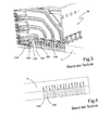
Figur 1 zeigt eine isometrische Ansicht von Kontaktelementen 10a, 10b eines mehrpoligen, mit einer Multilayerplatine 11 kontaktierten Steckverbinders gemäß dem Stand der Technik. Die Kontaktelemente 10a, 10b sind jeweils paarweise zusammengefasst. In Kontaktspaltenrichtung 12 sind vier Kontaktelementpaare angeordnet, wobei zehn Spalten in Kontaktreihenrichtung 13 vorgesehen sind. Die Anschluss-Stifte 14a, 14b der Kontaktelemente 10a, 10b sind in Bohrungen 15a, 15b der Multilayerplatine 11 verankert. Auf der obersten Leiterbahnebene 16 der Multilayerplatine 11, die mit der Oberfläche der Multilayerplatine 11 zusammenfällt, sind zwei Leiterbahnen 17a, 17b bezeichnet, die mit den Anschluss-Stiften 14a, 14b der Kontaktelemente 10a, 10b kontaktiert sind. Die Leiterbahnen 17a, 17b führen zu weiteren, nicht näher gezeigten Komponenten, die auf der Multilayerplatine 11 angeordnet sein können. -
Figur 2 zeigt eine Draufsicht auf die oberste Leiterbahnebene 16 der inFigur 1 gezeigten Multilayerplatine 11, die der Oberfläche der Multilayerplatine 11 entspricht. Deutlich sichtbar sind Krümmungen 20a, 20b der zu den Bohrungen 15a, 15b führenden Leiterbahnen 17a, 17b. Die Krümmungen 20a, 20b sind erforderlich, um eine kreuzungsfreie Führung der Leiterbahnen 17a, 17b zu ermöglichen. -
Figur 3 zeigt eine isometrische Ansicht eines Schnitts durch einen Steckverbinder 30 gemäß dem Stand der Technik mit den inFigur 1 gezeigten Kontaktelementen 10a, 10b. InFigur 3 ist die Verankerung der Anschluss-Stifte 14a, 14b der Kontaktelemente 10a, 10b in den Bohrungen 15a, 15b der Multilayerplatine 11 verdeutlicht. Demnach sind die Bohrungen 15a, 15b durch die Multilayerplatine 11 gebohrt. Dieser Sachverhalt ist inFigur 4 , die einen Schnitt durch die Bohrungen 15a, 15b in der Multilayerplatine 11 darstellt, nochmals verdeutlicht. - Gemäß dem Stand der Technik kann die Multilayerplatine 11 nicht näher gezeigte Leiterbahnen aufweisen, die in unterschiedlichen Leiterbahnebenen verlaufen. Aufgrund der jeweils durch die Multilayerplatine 11 gebohrten Bohrungen 15a, 15b sind bei den in gegebenenfalls unterschiedlichen Leiterbahnebenen angeordneten Leiterbahnen eine Vielzahl von Krümmungen erforderlich, von denen beispielhaft die Krümmungen 20a, 20b der Leiterbahnen 17a, 17b in
Figur 2 gezeigt sind. - Bei der in
Figur 5 gezeigten isometrischen Ansicht einer Vielzahl von Kontaktelementen 50a, 50b - 50'a, 50'b eines mehrpoligen, mit einer Multilayerplatine 51 kontaktierten Steckverbinders gemäß der Erfindung sind beispielhaft die Leiterbahnen 52a, 52b der Kontaktelemente 50a, 50b gezeigt, die in gerader Linie ohne Krümmungen von den inFigur 5 nicht sichtbaren Anschluss-Stiften 53a, 53b der Kontaktelemente 50a, 50b auf der obersten Leiterbahnebene 54 der Multilayerplatine 51 weggeführt sind, wobei die oberste Leiterbahnebene 54 exemplarisch zugleich der Oberfläche der erfindungsgemäßen Multilayerplatine 51 entspricht. - Die Kontaktelemente 50a, 50b - 50'a, 50'b sind paarweise jeweils in Kontaktreihenrichtung 13 angeordnet, wobei im gezeigten Ausführungsbeispiel sechs Kontaktelementpaare in Kontaktreihenrichtung 13 und acht Kontaktelementpaare in Kontaktspaltenrichtung 12 angeordnet sind. Diejenigen in
Figur 5 gezeigten Teile, die mit den in den vorangegangenen Figuren gezeigten Teilen übereinstimmen, tragen jeweils dieselben Bezugszeichen. Dieselbe Vereinbarung gilt sinngemäß insbesondere auch für die folgenden Figuren. - Die in
Figur 6 gezeigte Draufsicht auf die oberste Leiterbahnebene 54 der erfindungsgemäßen Multilayerplatine 51 verdeutlicht die in gerader Linie verlaufende Führung der Leiterbahnen 52a, 52b der zu den Bohrungen 60a, 60b führenden Leiterbahnen 52a, 52b, in welchen die Anschluss-Stifte 53a, 53b der Kontaktelemente 50a, 50b jeweils verankert sind. - Die Möglichkeit zur geradlinig verlaufenden Führung der Leiterbahnen 52a, 52b wird anhand von
Figur 7 deutlich, die eine isometrische Ansicht eines Schnitts durch die erfindungsgemäße Multilayerplatine 51 zeigt. Anstelle der in denFiguren 5 und 6 gezeigten Leiterbahnen 52a, 52b auf der Oberfläche der Multilayerplatine 51 sollen beispielhaft nunmehr Leiterbahnen 72a, 72b - 72'a, 72'b (siehe auchFigur 12 ) vorgesehen sein, die innerhalb der Multilayerplatine 51 in unterschiedlichen Leitbahnebenen 71 - 71' liegen. Die Bohrungen 60a - 60'a in der Multilayerplatine 51 sind als Sacklochbohrungen ausgeführt, wobei die in den unterschiedlichen Leiterbahnebenen 71 - 71' geführten Leiterbahnen 72a, 72b - 72'a, 72'b zu den einzelnen Sacklochbohrungen 60a, 60b - 60'a, 60'b geführt sind. InFigur 7 sind aufgrund des Schnitts nur die Leiterbahnen 72a - 72b und die Sacklochbohrungen 60a - 60'a zu sehen. Die Längen der Anschluss-Stifte 53a, 53b - 53'a, 53'b der Kontaktelemente 50a, 50b - 50'a, 50'b sind auf die Sacklochbohrungen 60a, 60b - 60'a, 60'b derart abzustimmen, dass die Anschluss-Stifte 53a, 53b - 53'a, 53'b maximal die Länge der zugehörenden Sacklochbohrungen 60a, 60b - 60'a, 60'b aufweisen. -
Figur 8 , die einen Schnitt durch die inFigur 7 dargestellten Multilayerplatine 51 zeigt, verdeutlicht die Sacklochbohrungen 60a, 60b - 60'a, 60'b, wobei aufgrund des Schnitts nur die Sacklochbohrungen 60a - 60'a zu sehen sind, die in jeweils unterschiedlichen Leiterbahnebenen 71 - 71' enden, in welchen jeweils die Leiterbahnen 72a, 72b - 72'a, 72'b untergebracht sind, wovon die Leiterbahnen 72a - 72'a zu sehen sind. Die Leiterbahnen 72a, 72b - 72'a, 72'b stellen jeweils die Verbindungen zu den in den Sacklochbohrungen 60a, 60b - 60'a, 60'b vorhandenen, inFigur 8 nicht gezeigten Anschluss-Stiften 53a, 53b - 53'a, 53'b der Kontaktelemente 50a, 50b - 50'a, 50'b her, wobei in den Sacklochbohrungen 60a, 60b - 60'a, 60'b beispielsweise Metallisierungen vorhanden sind, die den elektrischen Kontakt zu den zu verlötenden oder vorzugsweise zu verpressenden Anschluss-Stiften 53a, 53b - 53'a, 53'b ermöglichen. - Die
Figuren 7 und 8 zeigen die vorteilhafte Ausgestaltung der paarweisen Anordnung von Kontaktelementen 50a, 50b - 50'a, 50'b, wobei ein Kontaktelementpaar 50a, 50b - 50'a, 50'b vorzugsweise Differenzsignale führt. Dadurch, dass die beiden Kontaktelemente 50a, 50b - 50'a, 50'b eines Kontaktelementpaares nebeneinander in Kontaktreihenrichtung 13 angeordnet sind, kann sichergestellt werden, dass für die über ein Kontaktelementpaar 50a, 50b - 50'a, 50'b geführten Differenzsignale jeweils dieselbe Länge der Kontaktelemente 50a, 50b - 50'a, 50'b bis zu den Anschluss-Stiften 53a, 53b - 53'a, 53'b in den Sacklöchern 60a, 60b - 60'a, 60'b zur Verfügung steht. Damit wird ein vollständig symmetrischer Aufbau von Kontaktelementpaaren 50a, 50b - 50'a, 50'b erreicht, der eine Beaufschlagung der Kontaktelementpaaren 50a, 50b - 50'a, 50'b des erfindungsgemäßen Steckverbinders und/oder der erfindungsgemäßen Multilayerplatine und/oder der erfindungsgemäßen Kombination aus mehrpoligem Steckverbinder und Multilayerplatine mit sehr hohen Signalfrequenzen ermöglicht, bei denen nur äußerst geringe Signal-Laufzeitdifferenzen zwischen den Differenzsignalen auftreten dürfen. Es können hierbei digitale Signale im Bereich bis 40 GBit/s fehlerfrei übertragen werden. - Hierbei spielt die Vorgabe eines bestimmten Wellenwiderstands, beispielsweise 50 Ohm, für ein Kontaktelementpaar 50a, 50b - 50'a, 50'b ebenfalls eine Rolle, wobei der Wellenwiderstand, dessen Definition dem bereits erwähnten Fachbuch von Meincke und Gundlach entnommen werden kann, durch die geometrische Ausgestaltung der Kontaktelemente 50a, 50b - 50'a, 50'b, also deren Form und Abstand zueinander, sowie durch das zwischen dem Kontaktelementpaar 50a, 50b - 50'a, 50'b vorhandene Dielektrikum wesentlich beeinflusst wird. Der Wellenwiderstand kann jedoch auch innerhalb der Multilayerplatine 51 durch die entsprechenden Bemessungen der Leiterbahnen 72a, 72b - 72'a, 72'b mittels Vorgabe der genannten Kenngrößen eingestellt werden. Eine Minimierung der Signal-Laufzeitdifferenz wird auch im Bereich der Leiterbahnen 52a, 52b; 72a, 72b - 72'a, 72'b hauptsächlich durch die nunmehr mögliche geradlinige Führung der einzelnen Leiterbahnen 52a, 52b; 72a, 72b - 72'a, 72'b erzielt, wobei insbesondere die geradlinige und parallele Leiterbahnführung der zu einem Kontaktelementpaar 50a, 50b - 50'a, 50'b führenden Leiterbahnen 52a, 52b; 72a, 72b - 72'a, 72'b einen entscheidenden Beitrag zur Laufzeitminimierung liefert.
-
Figur 9 zeigt eine vollständige Ansicht des erfindungsgemäßen Steckverbinders 90, der mit der erfindungsgemäßen Multilayerplatine 51 kontaktiert ist. Bezeichnet ist ein Kontaktelementpaar 50a, 50b, das gemäß dem gezeigten Ausführungsbeispiel von einer Steckverbinderführung 91 zur Führung eines korrespondierenden Steckverbinders zumindest teilweise umgeben sein kann. Zur Verdeutlichung des Aufbaus des erfindungsgemäßen Steckverbinders 90 zeigtFigur 10 eine isometrische Ansicht eines Segments des inFigur 9 gezeigten Steckverbinders 90, wobei zusätzlich der Kontaktierungsbereich mit den in den Sacklochbohrungen 60 - 60' eingepressten Anschluss-Stiften 53a - 53'a sowie die zu den Sacklochbohrungen 60a - 60'a führenden Leiterbahnen 72a - 72'a zu sehen sind. -
Figur 11 verdeutlicht eine Ausgestaltung, bei welcher die Sacklochbohrungen 60a - 60'a nur teilweise von den Anschluss-Stiften 53a - 53'a der Kontaktelemente 50a - 50'a ausgefüllt werden. Unter der Zugrundelegung der Abstufung der Sacklochbohrungen 60a - 60'a hinsichtlich ihrer Tiefe, wobei die größte Tiefe am Rand der Multilayerplatine 51 vorgegeben sein soll, wird bei diesem Ausführungsbeispiel der Anschluss-Stift 53a seine zugehörende Sacklochbohrung 60a nahezu vollständig ausfüllen, während der Anschluss-Stift 53'a des Kontaktelements 50'a seine zugehörende Sacklochbohrung 60'a nur unvollständig ausfüllt. Der Vorteil dieser Ausgestaltung liegt darin, dass die Anschluss-Stifte 53a, 53b - 53'a, 53'b der Kontaktelemente 50a, 50b - 50'a, 50'b jeweils identisch realisiert sein können. - Eine hierzu alternative Ausgestaltung ist in
Figur 12 gezeigt, bei welcher die Anschluss-Stifte 53a, 53b - 53'a, 53'b jeweils mit einer Länge realisiert sind, welche die inFigur 12 nicht gezeigten Sacklochbohrungen 60a, 60b - 60'a, 60'b jeweils wenigstens näherungsweise vollständig ausfüllt. Der Vorteil bei dieser Ausgestaltung liegt darin, dass die mechanische Festigkeit des auf der erfindungsgemäßen Multilayerplatine 51 kontaktierten erfindungsgemäßen Steckverbinders 90 durch das nahezu vollständige Ausfüllen der Sacklochbohrungen 60a, 60b - 60'a, 60'b erhöht ist, sodass das gesamte System eine hohe Auszugskraft bereitstellen kann. Die Darstellung inFigur 12 ist derart gewählt, dass die in den unterschiedlichen Leiterbahnebenen angeordneten Leiterbahnen von Kontaktelementpaaren dargestellt werden können, wovon exemplarisch die in der obersten Leiterbahnebene angeordneten Leiterbahnen 72a, 72b des Kontaktelementpaars 50a, 50b und die in der untersten Leiterbahnebene angeordneten Leiterbahnen 72'a, 72'b des Kontaktelementpaars 50'a, 50'b bezeichnet sind.
Claims (17)
- Mehrpoliger Steckverbinder zur Kontaktierung mit einer Multilayerplatine (51), der eine Vielzahl von Kontaktelementen (50a, 50b - 50'a, 50'b) aufweist, dadurch gekennzeichnet, dass die Anschluss-Stifte (53a, 53b - 53'a, 53'b) der Kontaktelemente (50a, 50b - 50'a, 50'b) unterschiedlich lang sind zur Kontaktierung der Anschluss-Stifte (53a, 53b - 53'a, 53'b) mit in unterschiedlichen Leiterbahnebenen (71 - 71') vorgesehenen Leiterbahnen (52a, 52b; 72a, 72b - 72'a, 72'b) der Multilayerplatine (51).
- Mehrpoliger Steckverbinder zur Kontaktierung mit einer Multilayerplatine (51) nach Anspruch 1, dadurch gekennzeichnet, dass diejenigen Anschluss-Stifte des Steckverbinders (90), die zur Kontaktierung mit der Multilayerplatine (51) näher am Rand der Multilayerplatine (51) vorgesehen sind, am längsten sind und dahinter in Stufen jeweils weniger lang enden.
- Mehrpoliger Steckverbinder zur Kontaktierung mit einer Multilayerplatine (51) nach Anspruch 1 oder Anspruch 2, dadurch gekennzeichnet, dass die Anschluss-Stifte (53a, 53b - 53'a, 53'b) von Kontaktelementpaaren (50a, 50b - 50'a, 50'b), die in einer Kontaktelementreihe (13) des Steckverbinders (90) nebeneinander angeordnet sind, jeweils gleich lang sind.
- Mehrpoliger Steckverbinder zur Kontaktierung mit einer Multilayerplatine (51) nach einem der vorhergehenden Ansprüche, dadurch gekennzeichnet, dass die Anschluss-Stifte (53a, 53b - 53'a, 53'b) der in einer Kontaktelementreihe (13) liegenden Kontaktelemente (50a, 50b - 50'a, 50'b) des Steckverbinders (90) jeweils gleich lang sind.
- Mehrpoliger Steckverbinder zur Kontaktierung mit einer Multilayerplatine (51) nach Anspruch 3, dadurch gekennzeichnet, dass die Kontaktelementpaare (50a, 50b - 50'a, 50'b) Differenzsignale führen.
- Mehrpoliger Steckverbinder zur Kontaktierung mit einer Multilayerplatine (51) nach Anspruch 3, dadurch gekennzeichnet, dass die Kontaktelementpaare (50a, 50b - 50'a, 50'b) mit einem vorgegebenen Wellenwiderstand realisiert sind.
- Multilayerplatine zur Bestückung mit einem mehrpoligen Steckverbinder (90), die Sacklochbohrungen (60a, 60b - 60'a, 60'b) zur Kontaktierung von Anschluss-Stiften (53a, 53b - 53'a, 53'b) der Kontaktelemente (50a, 50b - 50'a, 50'b) des mehrpoligen Steckverbinders (90) aufweist, dadurch gekennzeichnet, dass die Sacklochbohrungen (60a, 60b - 60'a, 60'b) in unterschiedlichen Leiterbahnebenen (71 - 71') der Multilayerplatine (51) zur gezielten Kontaktierung der Anschluss-Stifte (53a, 53b - 53'a, 53'b) der Kontaktelemente (50a, 50b - 50'a, 50'b) mit in unterschiedlichen Leiterbahnebenen (71 - 71') vorgesehenen Leiterbahnen (52a, 52b; 72a, 72b - 72'a, 72'b) der Multilayerplatine (51) enden.
- Multilayerplatine zur Bestückung mit einem mehrpoligen Steckverbinder (90) nach Anspruch 7, dadurch gekennzeichnet, dass die Sacklochbohrungen (60a, 60b - 60'a, 60'b) am Rand der Multilayerplatine (51) am tiefsten sind und dahinter in Stufen jeweils weniger tief enden.
- Multilayerplatine zur Bestückung mit einem mehrpoligen Steckverbinder (90) nach Anspruch 7 oder Anspruch 8, dadurch gekennzeichnet, dass die Sacklochbohrungen (60a, 60b - 60'a, 60'b), die zur Kontaktierung mit Anschluss-Stiften (53a, 53b - 53'a, 53'b) von Kontaktelementpaaren (50a, 50b - 50'a, 50'b), die in einer Kontaktelementreihe (13) des Steckverbinders (90) nebeneinander angeordnet sind, jeweils gleich tief in der Multilayerplatine (51) enden.
- Multilayerplatine zur Bestückung mit einem mehrpoligen Steckverbinder (90) nach einem der Ansprüche 7 bis 9, dadurch gekennzeichnet, dass die Sacklochbohrungen (60a, 60b - 60'a, 60'b), die zur Kontaktierung der Anschluss-Stifte (53a, 53b - 53'a, 53'b) der in einer Kontaktelementreihe (13) liegenden Kontaktelemente (50a, 50b - 50'a, 50'b) des Steckverbinders (90) vorgesehen sind, jeweils gleich tief in der Multilayerplatine (51) enden.
- Multilayerplatine zur Bestückung mit einem mehrpoligen Steckverinder (90) nach Anspruch 9, dadurch gekennzeichnet, dass die Kontaktelementpaare (50a, 50b - 50'a, 50'b) Differenzsignale führen.
- Multilayerplatine zur Bestückung mit einem mehrpoligen Steckverbinder (90) nach Anspruch 9, dadurch gekennzeichnet, dass die den Kontaktelementpaaren (50a, 50b - 50'a, 50'b) zugeordneten Leiterbahnen (52a, 52b; 72a, 72b - 72'a, 72'b) wenigstens näherungsweise denselben Wellenwiderstand wie die entsprechenden Kontaktelementpaare (50a, 50b - 50'a, 50'b) im Steckverbinder (90) aufweisen.
- Kombination aus mehrpoligem Steckverbinder und Multilayerplatine (51), wobei der Steckverbinder eine Vielzahl von Kontaktelementen (50a, 50b - 50'a, 50'b) aufweist, und die Multilayerplatine (51) Sacklochbohrungen (60a, 60b - 60'a, 60'b) zur Kontaktierung von Anschluss-Stiften (53a, 53b - 53'a, 53'b) der Kontaktelemente (50a, 50b -50'a, 50'b) des mehrpoligen Steckverbinders (90) aufweist, dadurch gekennzeichnet, dass die Anschluss-Stifte (53a, 53b - 53'a, 53'b) der Kontaktelemente (50a, 50b - 50'a, 50'b) des Steckverbinders (90) unterschiedlich lang sind zur Kontaktierung der Anschluss-Stifte (53a, 53b - 53'a, 53'b) mit in unterschiedlichen Leiterbahnebenen (71 - 71') vorgesehenen Leiterbahnen (52a, 52b; 72a, 72b - 72'a, 72'b) der Multilayerplatine (51), und dass die Sacklochbohrungen (60a, 60b - 60'a, 60'b) in unterschiedlichen Leiterbahnebenen (71 - 71') der Multilayerplatine (51) zur gezielten Kontaktierung der in der Länge angepassten Anschluss-Stifte (53a, 53b - 53'a, 53'b) der Kontaktelemente (50a, 50b - 50'a, 50'b) enden.
- Kombination aus mehrpoligem Steckverbinder und Multilayerplatine (51) nach Anspruch 13, dadurch gekennzeichnet, dass die Anschluss-Stifte (53a, 53b - 53'a, 53'b) von Kontaktelementpaaren (50a, 50b - 50'a, 50'b), die in einer Kontaktelementreihe (13) des Steckverbinders (90) nebeneinander angeordnet sind, jeweils gleich lang sind.
- Kombination aus mehrpoligem Steckverbinder und Multilayerplatine (51) nach Anspruch 13 oder Anspruch 14, dadurch gekennzeichnet, dass die Anschluss-Stifte (53a, 53b - 53'a, 53'b) die zugehörenden Sacklochbohrungen (60a, 60b - 60'a, 60'b) wenigstens näherungsweise vollständig ausfüllen.
- Kombination aus mehrpoligem Steckverbinder und Multilayerplatine (51) nach Anspruch 14, dadurch gekennzeichnet, dass die Kontaktelementpaare (50a, 50b - 50'a, 50'b) Differenzsignale führen.
- Kombination aus mehrpoligem Steckverbinder und Multilayerplatine (51) nach Anspruch 14, dadurch gekennzeichnet, dass die Kontaktelementpaare (50a, 50b - 50'a, 50'b) mit einem vorgegebenen Wellenwiderstand realisiert sind.
Priority Applications (8)
| Application Number | Priority Date | Filing Date | Title |
|---|---|---|---|
| EP09011143A EP2290753B1 (de) | 2009-08-31 | 2009-08-31 | Steckverbinder und Multilayerplatine |
| DK09011143.6T DK2290753T3 (da) | 2009-08-31 | 2009-08-31 | Konnektor og flerlagsprintplade |
| PCT/EP2010/005033 WO2011023317A1 (de) | 2009-08-31 | 2010-08-17 | Steckverbinder und multilayerplatine |
| JP2012525907A JP5663773B2 (ja) | 2009-08-31 | 2010-08-17 | プラグコネクタ及び多層回路基板 |
| CN201080045066.2A CN102726125B (zh) | 2009-08-31 | 2010-08-17 | 插式连接器和多层电路板 |
| CA2772312A CA2772312C (en) | 2009-08-31 | 2010-08-17 | Plug connector and multi-layer circuit board |
| US13/392,933 US8622751B2 (en) | 2009-08-31 | 2010-08-17 | Plug connector and multi-layer circuit board |
| KR1020127007972A KR101691360B1 (ko) | 2009-08-31 | 2010-08-17 | 플러그 커넥터 및 다층 회로 기판 |
Applications Claiming Priority (1)
| Application Number | Priority Date | Filing Date | Title |
|---|---|---|---|
| EP09011143A EP2290753B1 (de) | 2009-08-31 | 2009-08-31 | Steckverbinder und Multilayerplatine |
Publications (2)
| Publication Number | Publication Date |
|---|---|
| EP2290753A1 true EP2290753A1 (de) | 2011-03-02 |
| EP2290753B1 EP2290753B1 (de) | 2012-12-05 |
Family
ID=41477650
Family Applications (1)
| Application Number | Title | Priority Date | Filing Date |
|---|---|---|---|
| EP09011143A Active EP2290753B1 (de) | 2009-08-31 | 2009-08-31 | Steckverbinder und Multilayerplatine |
Country Status (8)
| Country | Link |
|---|---|
| US (1) | US8622751B2 (de) |
| EP (1) | EP2290753B1 (de) |
| JP (1) | JP5663773B2 (de) |
| KR (1) | KR101691360B1 (de) |
| CN (1) | CN102726125B (de) |
| CA (1) | CA2772312C (de) |
| DK (1) | DK2290753T3 (de) |
| WO (1) | WO2011023317A1 (de) |
Families Citing this family (7)
| Publication number | Priority date | Publication date | Assignee | Title |
|---|---|---|---|---|
| DE102014109867A1 (de) * | 2014-07-14 | 2016-01-14 | Erni Production Gmbh & Co. Kg | Steckverbinder und Bauelement |
| CN105161879A (zh) * | 2015-09-24 | 2015-12-16 | 上海埃而生电气有限公司 | 多层pcb中央配电盒 |
| US10283885B2 (en) * | 2015-11-06 | 2019-05-07 | Foxconn Interconnect Technology Limited | Electrical connector assembly and system using the same |
| JP2019012586A (ja) * | 2015-11-17 | 2019-01-24 | 株式会社ジェイエイアイコーポレーション | コネクタ構造体 |
| CN106771831B (zh) * | 2017-01-09 | 2023-09-01 | 昆山艾伯格机器人科技有限公司 | 多种针高的连接器的自动检测机构 |
| CN107369932A (zh) * | 2017-08-08 | 2017-11-21 | 四川华丰企业集团有限公司 | 具有多层布线印制板的高速背板连接器 |
| US11664626B2 (en) * | 2021-07-29 | 2023-05-30 | Dell Products L.P. | Staggered press-fit fish-eye connector |
Citations (10)
| Publication number | Priority date | Publication date | Assignee | Title |
|---|---|---|---|---|
| DE4002025A1 (de) | 1989-01-26 | 1990-08-02 | Teradyne Inc | Gedruckte schaltungsplatte |
| DE29601655U1 (de) | 1996-01-31 | 1996-03-28 | Siemens AG, 80333 München | Baugruppenleiterplatte mit Steckverbinder |
| DE19604432A1 (de) * | 1996-02-07 | 1997-08-14 | Siemens Ag | Kontaktierung einer Leiterplatte mittels Einführkontakten und Druckkontakten |
| DE19807713A1 (de) | 1997-12-06 | 1999-06-17 | Erni Elektroapp | Steckverbinder für Backplanes und Einschubkarten bei sogenannten Compact PCI-Systemen |
| DE19902950A1 (de) | 1998-06-24 | 1999-12-30 | Wuerth Elektronik Gmbh & Co Kg | Verfahren zum Herstellen einer Leiterplatte und Leiterplatte |
| DE10040303A1 (de) | 2000-08-17 | 2002-04-04 | Volker Nissen | Verfahren zum definierten Tiefenbohren von Sacklöchern (blind vias) in mehrlagigen Leiterplatten (Multilayer) |
| US6817870B1 (en) | 2003-06-12 | 2004-11-16 | Nortel Networks Limited | Technique for interconnecting multilayer circuit boards |
| DE69915882T2 (de) | 1998-11-24 | 2005-03-03 | Teradyne, Inc., Boston | Elektrischer verbinder |
| US6976886B2 (en) | 2001-11-14 | 2005-12-20 | Fci Americas Technology, Inc. | Cross talk reduction and impedance-matching for high speed electrical connectors |
| DE102007060429A1 (de) * | 2007-12-14 | 2009-06-18 | Continental Automotive Gmbh | Elektronisches Modul, insbesondere Steuergerät für ein Kraftfahrzeug |
Family Cites Families (28)
| Publication number | Priority date | Publication date | Assignee | Title |
|---|---|---|---|---|
| US3660726A (en) * | 1970-10-12 | 1972-05-02 | Elfab Corp | Multi-layer printed circuit board and method of manufacture |
| JPS5758701Y2 (de) * | 1978-12-30 | 1982-12-15 | ||
| US4707039A (en) * | 1984-04-11 | 1987-11-17 | John Fluke Mfg. Co., Inc. | Coaxial connector for controlled impedance transmission lines |
| JPS6177286A (ja) * | 1984-09-21 | 1986-04-19 | インタ−ナショナル ビジネス マシ−ンズ コ−ポレ−ション | 同軸ケーブル用インターフェース装置 |
| FR2647971B1 (fr) * | 1989-06-01 | 1991-09-20 | Itt Composants Instr | Ensemble de connexion pour cartes a circuits imprimes |
| SE466126B (sv) * | 1990-12-21 | 1991-12-16 | Vemako Ab | Flerpoligt skaermat kontaktdon med gemensam jord |
| US5201662A (en) * | 1991-08-23 | 1993-04-13 | Molex Incorporated | Electrical connector for mounting on a printed circuit board |
| US5241454A (en) * | 1992-01-22 | 1993-08-31 | International Business Machines Corporation | Mutlilayered flexible circuit package |
| DE4217205C2 (de) * | 1992-05-23 | 1994-09-08 | Amphenol Tuchel Elect | Steckverbinder |
| JPH06163123A (ja) * | 1992-11-26 | 1994-06-10 | Nec Corp | 多極コネクタ |
| US5543586A (en) * | 1994-03-11 | 1996-08-06 | The Panda Project | Apparatus having inner layers supporting surface-mount components |
| DE69413679T2 (de) * | 1994-07-15 | 1999-04-29 | Berg Electronics Manufacturing B.V., S'-Hertogenbosch | Zusammenbau eines abgeschirmten Verbinders und einer Leiterplatte mit kontaktierten Löchern |
| JPH09139264A (ja) * | 1995-11-13 | 1997-05-27 | Yazaki Corp | Pcb用多極コネクタ |
| US5819401A (en) * | 1996-06-06 | 1998-10-13 | Texas Instruments Incorporated | Metal constrained circuit board side to side interconnection technique |
| US6538538B2 (en) * | 1999-02-25 | 2003-03-25 | Formfactor, Inc. | High frequency printed circuit board via |
| US6280201B1 (en) * | 2000-01-21 | 2001-08-28 | Hewlett-Packard Company | Laminated 90-degree connector |
| US6822874B1 (en) * | 2002-11-12 | 2004-11-23 | Wooshcom Corporation | Modular high availability electronic product architecture with flexible I/O |
| US6971896B2 (en) * | 2004-01-08 | 2005-12-06 | International Business Machines Corporaion | Flex strips for high frequency connectors |
| JP3909769B2 (ja) * | 2004-01-09 | 2007-04-25 | 日本航空電子工業株式会社 | コネクタ |
| US7278855B2 (en) * | 2004-02-09 | 2007-10-09 | Silicon Pipe, Inc | High speed, direct path, stair-step, electronic connectors with improved signal integrity characteristics and methods for their manufacture |
| DE102004050687B4 (de) * | 2004-10-18 | 2019-01-31 | Continental Automotive Gmbh | Kontaktierungsanordnung für eine flexible Leiterplatte und deren Verwendung |
| EP1910737A1 (de) * | 2005-07-14 | 2008-04-16 | Tir Systems Ltd. | Stromtafel und einschub-beleuchtungsmodul |
| US7497703B2 (en) * | 2005-09-12 | 2009-03-03 | Tyco Electronics Corporation | Method and apparatus for providing symmetrical signal return path in differential systems |
| US7878854B2 (en) * | 2008-07-21 | 2011-02-01 | Tyco Electronics Corporation | Electrical connector having variable length mounting contacts |
| DK2207244T3 (da) * | 2009-01-12 | 2014-04-22 | Erni Electronics Gmbh & Co Kg | Indretning omfattende stikforbinder og flerlagsprintplade |
| JP5310239B2 (ja) * | 2009-05-09 | 2013-10-09 | 富士通株式会社 | 接続端子および伝送線路 |
| US8057240B2 (en) * | 2010-03-23 | 2011-11-15 | Tyco Electronics Corporation | Circuit board for an electrical connector assembly |
| US8657627B2 (en) * | 2011-02-02 | 2014-02-25 | Amphenol Corporation | Mezzanine connector |
-
2009
- 2009-08-31 DK DK09011143.6T patent/DK2290753T3/da active
- 2009-08-31 EP EP09011143A patent/EP2290753B1/de active Active
-
2010
- 2010-08-17 CN CN201080045066.2A patent/CN102726125B/zh active Active
- 2010-08-17 US US13/392,933 patent/US8622751B2/en active Active
- 2010-08-17 WO PCT/EP2010/005033 patent/WO2011023317A1/de not_active Ceased
- 2010-08-17 CA CA2772312A patent/CA2772312C/en not_active Expired - Fee Related
- 2010-08-17 KR KR1020127007972A patent/KR101691360B1/ko active Active
- 2010-08-17 JP JP2012525907A patent/JP5663773B2/ja active Active
Patent Citations (10)
| Publication number | Priority date | Publication date | Assignee | Title |
|---|---|---|---|---|
| DE4002025A1 (de) | 1989-01-26 | 1990-08-02 | Teradyne Inc | Gedruckte schaltungsplatte |
| DE29601655U1 (de) | 1996-01-31 | 1996-03-28 | Siemens AG, 80333 München | Baugruppenleiterplatte mit Steckverbinder |
| DE19604432A1 (de) * | 1996-02-07 | 1997-08-14 | Siemens Ag | Kontaktierung einer Leiterplatte mittels Einführkontakten und Druckkontakten |
| DE19807713A1 (de) | 1997-12-06 | 1999-06-17 | Erni Elektroapp | Steckverbinder für Backplanes und Einschubkarten bei sogenannten Compact PCI-Systemen |
| DE19902950A1 (de) | 1998-06-24 | 1999-12-30 | Wuerth Elektronik Gmbh & Co Kg | Verfahren zum Herstellen einer Leiterplatte und Leiterplatte |
| DE69915882T2 (de) | 1998-11-24 | 2005-03-03 | Teradyne, Inc., Boston | Elektrischer verbinder |
| DE10040303A1 (de) | 2000-08-17 | 2002-04-04 | Volker Nissen | Verfahren zum definierten Tiefenbohren von Sacklöchern (blind vias) in mehrlagigen Leiterplatten (Multilayer) |
| US6976886B2 (en) | 2001-11-14 | 2005-12-20 | Fci Americas Technology, Inc. | Cross talk reduction and impedance-matching for high speed electrical connectors |
| US6817870B1 (en) | 2003-06-12 | 2004-11-16 | Nortel Networks Limited | Technique for interconnecting multilayer circuit boards |
| DE102007060429A1 (de) * | 2007-12-14 | 2009-06-18 | Continental Automotive Gmbh | Elektronisches Modul, insbesondere Steuergerät für ein Kraftfahrzeug |
Non-Patent Citations (1)
| Title |
|---|
| MEINKE; GUNDLACH: "Taschenbuch für Hochfrequenztechnik", 1956, SPRINGER-VERLAG |
Also Published As
| Publication number | Publication date |
|---|---|
| DK2290753T3 (da) | 2013-03-18 |
| US20120184115A1 (en) | 2012-07-19 |
| JP5663773B2 (ja) | 2015-02-04 |
| KR101691360B1 (ko) | 2016-12-30 |
| KR20120060220A (ko) | 2012-06-11 |
| JP2013503418A (ja) | 2013-01-31 |
| EP2290753B1 (de) | 2012-12-05 |
| WO2011023317A1 (de) | 2011-03-03 |
| CA2772312C (en) | 2016-09-27 |
| US8622751B2 (en) | 2014-01-07 |
| CN102726125B (zh) | 2016-07-20 |
| CN102726125A (zh) | 2012-10-10 |
| CA2772312A1 (en) | 2011-03-03 |
Similar Documents
| Publication | Publication Date | Title |
|---|---|---|
| DE69915874T2 (de) | Gedruckte leiterplatte und verfahren zu deren herstellung | |
| DE102006056001B4 (de) | Konfektionierbarer Rundsteckverbinder für Ethernet | |
| EP2290753B1 (de) | Steckverbinder und Multilayerplatine | |
| EP2684253B1 (de) | Anschlussvorrichtung und anschlussverfahren für hochfrequente digitalsignale | |
| EP3170229A1 (de) | Steckverbinder und bauelement | |
| WO2003086033A1 (de) | Leiterplatte sowie verfahren zu ihrer herstellung | |
| WO2009138168A1 (de) | Leiterplatte für elektrischen verbinder und elektrischer verbinder | |
| DE112005002368T5 (de) | Eine Vorrichtung und ein Verfahren zum Verbessern der Signalebenenübergänge bei gedruckten Schaltkarten | |
| DE3447556A1 (de) | Multilayer-leiterverbindung | |
| DE112011101471T5 (de) | Leiterplatte mit durch leitfähige Durchkontaktierungen verbundenen Schichten | |
| EP3132660A1 (de) | Vorrichtung und verfahren zur signalübertragung von differentiellen datensignalen | |
| EP2979333B1 (de) | Steckverbinder mit übersprechkompensation | |
| DE19729162C2 (de) | Verbinder zwischen einer Tochterplatine und einer Mutterplatine | |
| EP2510586B1 (de) | Relief-steckverbinder und multilayerplatine | |
| DE60013659T2 (de) | Schaltungsplatte mit seitlichen Verbindungen | |
| DE60320446T2 (de) | Schaltung, die ein Differenzsignal abgreift | |
| DE102017202329A1 (de) | Multilayer-Leiterplatte sowie elektronische Anordnung mit einer solchen | |
| EP4056002A1 (de) | Elektrogerät, insbesondere wechselrichter oder umrichter | |
| WO2010071905A1 (de) | Verfahren zum design von signalleitungen in einer mehr-lagen-leiterplatte und solcherart hergestellte mehr-lagen-leiterplatte | |
| DE202014008844U1 (de) | Elektrisches Interface | |
| DE3412290A1 (de) | Mehrlagige leiterplatte in multilayer- oder stapeltechnik | |
| DE4326989A1 (de) | Leiterplatte | |
| EP3447854B1 (de) | Leiterplatte, verbindersystem und verfahren | |
| EP2200411A1 (de) | Leiterplatte | |
| EP1083434A2 (de) | Vorrichtung zum Prüfen von Leiterplatten |
Legal Events
| Date | Code | Title | Description |
|---|---|---|---|
| PUAI | Public reference made under article 153(3) epc to a published international application that has entered the european phase |
Free format text: ORIGINAL CODE: 0009012 |
|
| AK | Designated contracting states |
Kind code of ref document: A1 Designated state(s): AT BE BG CH CY CZ DE DK EE ES FI FR GB GR HR HU IE IS IT LI LT LU LV MC MK MT NL NO PL PT RO SE SI SK SM TR |
|
| AX | Request for extension of the european patent |
Extension state: AL BA RS |
|
| 17P | Request for examination filed |
Effective date: 20110822 |
|
| 17Q | First examination report despatched |
Effective date: 20120126 |
|
| RIC1 | Information provided on ipc code assigned before grant |
Ipc: H01R 12/72 20110101ALI20120629BHEP Ipc: H05K 1/02 20060101AFI20120629BHEP |
|
| GRAP | Despatch of communication of intention to grant a patent |
Free format text: ORIGINAL CODE: EPIDOSNIGR1 |
|
| GRAS | Grant fee paid |
Free format text: ORIGINAL CODE: EPIDOSNIGR3 |
|
| GRAA | (expected) grant |
Free format text: ORIGINAL CODE: 0009210 |
|
| AK | Designated contracting states |
Kind code of ref document: B1 Designated state(s): AT BE BG CH CY CZ DE DK EE ES FI FR GB GR HR HU IE IS IT LI LT LU LV MC MK MT NL NO PL PT RO SE SI SK SM TR |
|
| REG | Reference to a national code |
Ref country code: GB Ref legal event code: FG4D Free format text: NOT ENGLISH |
|
| REG | Reference to a national code |
Ref country code: CH Ref legal event code: EP |
|
| REG | Reference to a national code |
Ref country code: AT Ref legal event code: REF Ref document number: 587877 Country of ref document: AT Kind code of ref document: T Effective date: 20121215 |
|
| REG | Reference to a national code |
Ref country code: IE Ref legal event code: FG4D Free format text: LANGUAGE OF EP DOCUMENT: GERMAN |
|
| REG | Reference to a national code |
Ref country code: DE Ref legal event code: R096 Ref document number: 502009005549 Country of ref document: DE Effective date: 20130131 |
|
| REG | Reference to a national code |
Ref country code: DK Ref legal event code: T3 |
|
| REG | Reference to a national code |
Ref country code: SE Ref legal event code: TRGR |
|
| REG | Reference to a national code |
Ref country code: CH Ref legal event code: NV Representative=s name: RENTSCH PARTNER AG, CH |
|
| PG25 | Lapsed in a contracting state [announced via postgrant information from national office to epo] |
Ref country code: LT Free format text: LAPSE BECAUSE OF FAILURE TO SUBMIT A TRANSLATION OF THE DESCRIPTION OR TO PAY THE FEE WITHIN THE PRESCRIBED TIME-LIMIT Effective date: 20121205 Ref country code: ES Free format text: LAPSE BECAUSE OF FAILURE TO SUBMIT A TRANSLATION OF THE DESCRIPTION OR TO PAY THE FEE WITHIN THE PRESCRIBED TIME-LIMIT Effective date: 20130316 Ref country code: NO Free format text: LAPSE BECAUSE OF FAILURE TO SUBMIT A TRANSLATION OF THE DESCRIPTION OR TO PAY THE FEE WITHIN THE PRESCRIBED TIME-LIMIT Effective date: 20130305 |
|
| REG | Reference to a national code |
Ref country code: NL Ref legal event code: VDEP Effective date: 20121205 |
|
| REG | Reference to a national code |
Ref country code: NL Ref legal event code: T3 |
|
| REG | Reference to a national code |
Ref country code: LT Ref legal event code: MG4D |
|
| PG25 | Lapsed in a contracting state [announced via postgrant information from national office to epo] |
Ref country code: LV Free format text: LAPSE BECAUSE OF FAILURE TO SUBMIT A TRANSLATION OF THE DESCRIPTION OR TO PAY THE FEE WITHIN THE PRESCRIBED TIME-LIMIT Effective date: 20121205 Ref country code: SI Free format text: LAPSE BECAUSE OF FAILURE TO SUBMIT A TRANSLATION OF THE DESCRIPTION OR TO PAY THE FEE WITHIN THE PRESCRIBED TIME-LIMIT Effective date: 20121205 Ref country code: PL Free format text: LAPSE BECAUSE OF FAILURE TO SUBMIT A TRANSLATION OF THE DESCRIPTION OR TO PAY THE FEE WITHIN THE PRESCRIBED TIME-LIMIT Effective date: 20121205 Ref country code: GR Free format text: LAPSE BECAUSE OF FAILURE TO SUBMIT A TRANSLATION OF THE DESCRIPTION OR TO PAY THE FEE WITHIN THE PRESCRIBED TIME-LIMIT Effective date: 20130306 |
|
| PG25 | Lapsed in a contracting state [announced via postgrant information from national office to epo] |
Ref country code: BG Free format text: LAPSE BECAUSE OF FAILURE TO SUBMIT A TRANSLATION OF THE DESCRIPTION OR TO PAY THE FEE WITHIN THE PRESCRIBED TIME-LIMIT Effective date: 20130305 Ref country code: EE Free format text: LAPSE BECAUSE OF FAILURE TO SUBMIT A TRANSLATION OF THE DESCRIPTION OR TO PAY THE FEE WITHIN THE PRESCRIBED TIME-LIMIT Effective date: 20121205 Ref country code: SK Free format text: LAPSE BECAUSE OF FAILURE TO SUBMIT A TRANSLATION OF THE DESCRIPTION OR TO PAY THE FEE WITHIN THE PRESCRIBED TIME-LIMIT Effective date: 20121205 Ref country code: IS Free format text: LAPSE BECAUSE OF FAILURE TO SUBMIT A TRANSLATION OF THE DESCRIPTION OR TO PAY THE FEE WITHIN THE PRESCRIBED TIME-LIMIT Effective date: 20130405 Ref country code: CZ Free format text: LAPSE BECAUSE OF FAILURE TO SUBMIT A TRANSLATION OF THE DESCRIPTION OR TO PAY THE FEE WITHIN THE PRESCRIBED TIME-LIMIT Effective date: 20121205 |
|
| PG25 | Lapsed in a contracting state [announced via postgrant information from national office to epo] |
Ref country code: RO Free format text: LAPSE BECAUSE OF FAILURE TO SUBMIT A TRANSLATION OF THE DESCRIPTION OR TO PAY THE FEE WITHIN THE PRESCRIBED TIME-LIMIT Effective date: 20121205 Ref country code: PT Free format text: LAPSE BECAUSE OF FAILURE TO SUBMIT A TRANSLATION OF THE DESCRIPTION OR TO PAY THE FEE WITHIN THE PRESCRIBED TIME-LIMIT Effective date: 20130405 |
|
| PLBE | No opposition filed within time limit |
Free format text: ORIGINAL CODE: 0009261 |
|
| STAA | Information on the status of an ep patent application or granted ep patent |
Free format text: STATUS: NO OPPOSITION FILED WITHIN TIME LIMIT |
|
| RAP2 | Party data changed (patent owner data changed or rights of a patent transferred) |
Owner name: ERNI ELECTRONICS GMBH & CO. KG |
|
| 26N | No opposition filed |
Effective date: 20130906 |
|
| PG25 | Lapsed in a contracting state [announced via postgrant information from national office to epo] |
Ref country code: CY Free format text: LAPSE BECAUSE OF FAILURE TO SUBMIT A TRANSLATION OF THE DESCRIPTION OR TO PAY THE FEE WITHIN THE PRESCRIBED TIME-LIMIT Effective date: 20121205 Ref country code: HR Free format text: LAPSE BECAUSE OF FAILURE TO SUBMIT A TRANSLATION OF THE DESCRIPTION OR TO PAY THE FEE WITHIN THE PRESCRIBED TIME-LIMIT Effective date: 20121205 |
|
| REG | Reference to a national code |
Ref country code: DE Ref legal event code: R097 Ref document number: 502009005549 Country of ref document: DE Effective date: 20130906 |
|
| BERE | Be: lapsed |
Owner name: ERNI ELECTRONICS G.M.B.H. Effective date: 20130831 |
|
| PG25 | Lapsed in a contracting state [announced via postgrant information from national office to epo] |
Ref country code: MC Free format text: LAPSE BECAUSE OF FAILURE TO SUBMIT A TRANSLATION OF THE DESCRIPTION OR TO PAY THE FEE WITHIN THE PRESCRIBED TIME-LIMIT Effective date: 20121205 |
|
| REG | Reference to a national code |
Ref country code: IE Ref legal event code: MM4A |
|
| PG25 | Lapsed in a contracting state [announced via postgrant information from national office to epo] |
Ref country code: BE Free format text: LAPSE BECAUSE OF NON-PAYMENT OF DUE FEES Effective date: 20130831 |
|
| PG25 | Lapsed in a contracting state [announced via postgrant information from national office to epo] |
Ref country code: IE Free format text: LAPSE BECAUSE OF NON-PAYMENT OF DUE FEES Effective date: 20130831 |
|
| REG | Reference to a national code |
Ref country code: DE Ref legal event code: R082 Ref document number: 502009005549 Country of ref document: DE Representative=s name: JAKELSKI & ALTHOFF PATENTANWAELTE, DE |
|
| REG | Reference to a national code |
Ref country code: CH Ref legal event code: PFA Owner name: ERNI PRODUCTION GMBH AND CO. KG, DE Free format text: FORMER OWNER: ERNI ELECTRONICS GMBH, DE |
|
| REG | Reference to a national code |
Ref country code: DE Ref legal event code: R081 Ref document number: 502009005549 Country of ref document: DE Owner name: ERNI PRODUCTION GMBH CO. KG, DE Free format text: FORMER OWNER: ERNI ELECTRONICS GMBH, 73099 ADELBERG, DE Effective date: 20140827 Ref country code: DE Ref legal event code: R082 Ref document number: 502009005549 Country of ref document: DE Representative=s name: JAKELSKI & ALTHOFF PATENTANWAELTE PARTNERSCHAF, DE Effective date: 20140827 Ref country code: DE Ref legal event code: R082 Ref document number: 502009005549 Country of ref document: DE Representative=s name: JAKELSKI & ALTHOFF PATENTANWAELTE, DE Effective date: 20140827 Ref country code: DE Ref legal event code: R081 Ref document number: 502009005549 Country of ref document: DE Owner name: ERNI PRODUCTION GMBH & CO. KG, DE Free format text: FORMER OWNER: ERNI ELECTRONICS GMBH, 73099 ADELBERG, DE Effective date: 20140827 |
|
| REG | Reference to a national code |
Ref country code: FR Ref legal event code: CJ Effective date: 20141008 Ref country code: FR Ref legal event code: CD Owner name: ERNI PRODUCTION GMBH & CO. KG, DE Effective date: 20141008 |
|
| REG | Reference to a national code |
Ref country code: AT Ref legal event code: PC Ref document number: 587877 Country of ref document: AT Kind code of ref document: T Owner name: ERNI PRODUCTION GMBH & CO.KG, DE Effective date: 20140919 |
|
| REG | Reference to a national code |
Ref country code: NL Ref legal event code: TD Effective date: 20141201 Ref country code: NL Ref legal event code: SD Effective date: 20141201 |
|
| PG25 | Lapsed in a contracting state [announced via postgrant information from national office to epo] |
Ref country code: SM Free format text: LAPSE BECAUSE OF FAILURE TO SUBMIT A TRANSLATION OF THE DESCRIPTION OR TO PAY THE FEE WITHIN THE PRESCRIBED TIME-LIMIT Effective date: 20121205 |
|
| PG25 | Lapsed in a contracting state [announced via postgrant information from national office to epo] |
Ref country code: TR Free format text: LAPSE BECAUSE OF FAILURE TO SUBMIT A TRANSLATION OF THE DESCRIPTION OR TO PAY THE FEE WITHIN THE PRESCRIBED TIME-LIMIT Effective date: 20121205 Ref country code: MT Free format text: LAPSE BECAUSE OF FAILURE TO SUBMIT A TRANSLATION OF THE DESCRIPTION OR TO PAY THE FEE WITHIN THE PRESCRIBED TIME-LIMIT Effective date: 20121205 |
|
| PG25 | Lapsed in a contracting state [announced via postgrant information from national office to epo] |
Ref country code: LU Free format text: LAPSE BECAUSE OF NON-PAYMENT OF DUE FEES Effective date: 20130831 Ref country code: MK Free format text: LAPSE BECAUSE OF FAILURE TO SUBMIT A TRANSLATION OF THE DESCRIPTION OR TO PAY THE FEE WITHIN THE PRESCRIBED TIME-LIMIT Effective date: 20121205 Ref country code: HU Free format text: LAPSE BECAUSE OF FAILURE TO SUBMIT A TRANSLATION OF THE DESCRIPTION OR TO PAY THE FEE WITHIN THE PRESCRIBED TIME-LIMIT; INVALID AB INITIO Effective date: 20090831 |
|
| REG | Reference to a national code |
Ref country code: FR Ref legal event code: PLFP Year of fee payment: 8 |
|
| REG | Reference to a national code |
Ref country code: FR Ref legal event code: PLFP Year of fee payment: 9 |
|
| REG | Reference to a national code |
Ref country code: CH Ref legal event code: PCAR Free format text: NEW ADDRESS: BELLERIVESTRASSE 203 POSTFACH, 8034 ZUERICH (CH) |
|
| REG | Reference to a national code |
Ref country code: FR Ref legal event code: PLFP Year of fee payment: 10 |
|
| PGFP | Annual fee paid to national office [announced via postgrant information from national office to epo] |
Ref country code: CH Payment date: 20210824 Year of fee payment: 13 Ref country code: SE Payment date: 20210823 Year of fee payment: 13 |
|
| REG | Reference to a national code |
Ref country code: CH Ref legal event code: PL |
|
| PG25 | Lapsed in a contracting state [announced via postgrant information from national office to epo] |
Ref country code: LI Free format text: LAPSE BECAUSE OF NON-PAYMENT OF DUE FEES Effective date: 20220831 Ref country code: CH Free format text: LAPSE BECAUSE OF NON-PAYMENT OF DUE FEES Effective date: 20220831 |
|
| REG | Reference to a national code |
Ref country code: SE Ref legal event code: EUG |
|
| PG25 | Lapsed in a contracting state [announced via postgrant information from national office to epo] |
Ref country code: SE Free format text: LAPSE BECAUSE OF NON-PAYMENT OF DUE FEES Effective date: 20220901 |
|
| PGFP | Annual fee paid to national office [announced via postgrant information from national office to epo] |
Ref country code: NL Payment date: 20250704 Year of fee payment: 17 |
|
| PGFP | Annual fee paid to national office [announced via postgrant information from national office to epo] |
Ref country code: FI Payment date: 20250814 Year of fee payment: 17 |
|
| PGFP | Annual fee paid to national office [announced via postgrant information from national office to epo] |
Ref country code: DK Payment date: 20250814 Year of fee payment: 17 Ref country code: DE Payment date: 20250702 Year of fee payment: 17 |
|
| PGFP | Annual fee paid to national office [announced via postgrant information from national office to epo] |
Ref country code: IT Payment date: 20250722 Year of fee payment: 17 |
|
| PGFP | Annual fee paid to national office [announced via postgrant information from national office to epo] |
Ref country code: GB Payment date: 20250703 Year of fee payment: 17 |
|
| PGFP | Annual fee paid to national office [announced via postgrant information from national office to epo] |
Ref country code: FR Payment date: 20250703 Year of fee payment: 17 Ref country code: AT Payment date: 20250725 Year of fee payment: 17 |