EP2290438A1 - Elektrochrome Vorrichtungen mit verbesserten ionenleitenden Schichten - Google Patents
Elektrochrome Vorrichtungen mit verbesserten ionenleitenden Schichten Download PDFInfo
- Publication number
- EP2290438A1 EP2290438A1 EP10011284A EP10011284A EP2290438A1 EP 2290438 A1 EP2290438 A1 EP 2290438A1 EP 10011284 A EP10011284 A EP 10011284A EP 10011284 A EP10011284 A EP 10011284A EP 2290438 A1 EP2290438 A1 EP 2290438A1
- Authority
- EP
- European Patent Office
- Prior art keywords
- oxides
- layer
- oxide
- electrochromic device
- ion
- Prior art date
- Legal status (The legal status is an assumption and is not a legal conclusion. Google has not performed a legal analysis and makes no representation as to the accuracy of the status listed.)
- Withdrawn
Links
Images


Classifications
-
- G—PHYSICS
- G02—OPTICS
- G02F—OPTICAL DEVICES OR ARRANGEMENTS FOR THE CONTROL OF LIGHT BY MODIFICATION OF THE OPTICAL PROPERTIES OF THE MEDIA OF THE ELEMENTS INVOLVED THEREIN; NON-LINEAR OPTICS; FREQUENCY-CHANGING OF LIGHT; OPTICAL LOGIC ELEMENTS; OPTICAL ANALOGUE/DIGITAL CONVERTERS
- G02F1/00—Devices or arrangements for the control of the intensity, colour, phase, polarisation or direction of light arriving from an independent light source, e.g. switching, gating or modulating; Non-linear optics
- G02F1/01—Devices or arrangements for the control of the intensity, colour, phase, polarisation or direction of light arriving from an independent light source, e.g. switching, gating or modulating; Non-linear optics for the control of the intensity, phase, polarisation or colour
- G02F1/15—Devices or arrangements for the control of the intensity, colour, phase, polarisation or direction of light arriving from an independent light source, e.g. switching, gating or modulating; Non-linear optics for the control of the intensity, phase, polarisation or colour based on an electrochromic effect
- G02F1/1514—Devices or arrangements for the control of the intensity, colour, phase, polarisation or direction of light arriving from an independent light source, e.g. switching, gating or modulating; Non-linear optics for the control of the intensity, phase, polarisation or colour based on an electrochromic effect characterised by the electrochromic material, e.g. by the electrodeposited material
- G02F1/1523—Devices or arrangements for the control of the intensity, colour, phase, polarisation or direction of light arriving from an independent light source, e.g. switching, gating or modulating; Non-linear optics for the control of the intensity, phase, polarisation or colour based on an electrochromic effect characterised by the electrochromic material, e.g. by the electrodeposited material comprising inorganic material
- G02F1/1525—Devices or arrangements for the control of the intensity, colour, phase, polarisation or direction of light arriving from an independent light source, e.g. switching, gating or modulating; Non-linear optics for the control of the intensity, phase, polarisation or colour based on an electrochromic effect characterised by the electrochromic material, e.g. by the electrodeposited material comprising inorganic material characterised by a particular ion transporting layer, e.g. electrolyte
-
- G—PHYSICS
- G02—OPTICS
- G02F—OPTICAL DEVICES OR ARRANGEMENTS FOR THE CONTROL OF LIGHT BY MODIFICATION OF THE OPTICAL PROPERTIES OF THE MEDIA OF THE ELEMENTS INVOLVED THEREIN; NON-LINEAR OPTICS; FREQUENCY-CHANGING OF LIGHT; OPTICAL LOGIC ELEMENTS; OPTICAL ANALOGUE/DIGITAL CONVERTERS
- G02F2201/00—Constructional arrangements not provided for in groups G02F1/00 - G02F7/00
- G02F2201/16—Constructional arrangements not provided for in groups G02F1/00 - G02F7/00 series; tandem
Definitions
- the present invention relates to electrochromic devices and more particularly relates to solid-state, inorganic thin film electrochromic devices.
- Electrochromic materials and devices have been developed as an alternative to passive coating materials for light and heat management in building and vehicle windows.
- electrochromic devices employ materials capable of reversibly altering their optical properties following electrochemical oxidation and reduction in response to an applied potential.
- the optical modulation is the result of the simultaneous insertion and extraction of electrons and charge compensating ions in the electrochemical material lattice.
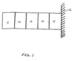
- FIG.1 illustrates a typical five layer solid-state electrochromic device in cross-section having the five following superimposed layers: an electrochromic electrode layer (“EC") 14 which produces a change in absorption or reflection upon oxidation or reduction; an ion conductor layer (“IC”) 13 which functionally replaces an electrolyte, allowing the passage of ions while blocking electronic current; a counter electrode layer (“CE”) 12 which serves as a storage layer for ions when the device is in the bleached or clear state; and two conductive layers (“CL”) 11 and 15 which serve to apply an electrical potential to the electrochromic device.
- EC electrochromic electrode layer
- IC ion conductor layer
- CE counter electrode layer
- CL conductive layers
- Merely increasing the thickness of the ion conductor layer may result in a reduction of leakage current, but at the expense of degraded optical properties, increased layer deposition time and cost, and reduced switching rates. Accordingly, it is desirable to reduce the amount of electronic leakage through an electrochromic device without resorting to a thick ion conductor layer so as to avoid these compromises in performance.
- FIG. 2 shows the equilibrium electrical and optical characteristics of an electrochromic device for applied voltages in the 'forward' or coloring polarity, up until the point where substantial electronic leakage current begins to flow. These characteristics are plotted as a function of the internal voltage, which is the voltage applied to the device minus the voltage induced in the series resistance as a result of the current flowing. Initially, there is a slow increase in the current density below a particular 'threshold voltage,' accompanied by an increase in optical density. Above the threshold voltage, however, the electrochromic device breaks down electronically and any additional current flowing is primarily electronic leakage. Moreover, reaching the threshold voltage prevents any further increases in voltage across the electrochromic device.
- the threshold voltage will determine the maximum obtainable optical density for a given device structure, i.e. a particular layer thickness, and, hence its dynamic range. As such, it is desirable to increase the voltage that can be developed across the ion conductor layer of the electrochromic device prior to it breaking down so as to allow electrochromic devices to color more deeply and to reduce power consumption.
- Takahashi (United States Patent No. 4,293,194 ) discloses a device having decreased electronic leakage.
- Takahashi teaches a solid electrochromic device incorporating an electron blocking material comprised of a layer of an N-type semiconductor adjacent to a layer of a P-type semiconductor.
- Takahashi does not teach a multi-layered thin film ion conductor layer capable of reducing electronic leakage while increasing the voltage that may be developed across the ion conductor layer.
- an electrochromic device comprising a first electrode comprising one of an electrochromic electrode layer and a counter electrode layer, a second electrode comprising the other of said electrochromic electrode layer and said counter electrode layer, an ion-conductor layer for conducting ions between the first and second electrodes comprising at least two ion transport layers and a buffer layer, the at least two ion transport layers and the buffer layer alternating within the ion conductor layer such that the ion transport layers are in communication with the first and second electrodes, said buffer layer comprising a mixture of a nickel oxide and a tungsten oxide, wherein the amount of said nickel oxide to the amount of said tungsten oxide ranges from about 25:1 to about 1:25, a first conductive layer, and a second conductive layer, wherein the first and second electrodes and the ion-conductor layer are sandwiched between the first and second conductive layers.
- adjacent ones of the at least two ion transport layers and buffer layer are comprised of different materials.
- the at least two ion transport layers are comprised of an insulator comprised of a material selected from the group consisting of silicon oxides, aluminum oxides, aluminum nitrides, niobium oxides, tantalum oxides, zirconium oxides, yttrium oxides, hafnium oxides, and mixtures thereof.
- the insulator is comprised of a material selected from the group consisting of SiO 2, Al 2 O 3 , Nb 2 O 3 , Ta 2 O 5 , LiTaO 3 , LiNbO 3 , La 2 TiO 7 , La2TiO 7 , SrZrO 3 , ZrO 2 , Y 2 O 3 , Nb 2 O 5 , La 2 Ti 2 O 7 , LaTiO 3 , HfPO 2 , and mixtures thereof.
- the insulator is a mixture of a silicon oxide and an aluminum oxide, wherein an amount of the silicon oxide to an amount of the aluminum oxide ranges from about 25:1 to about 1:25, preferably ranging from about 11:1 to about 17:1.
- the insulator is a mixture of a zirconium oxide and a yttrium oxide, wherein an amount of the zirconium oxide to an amount of the yttrium oxide ranges from about 25:1 to about 1:25.
- the at least two ion transport layers have a thickness ranging from about 1 nm to about 70 nm, preferably from about 5 nm to about 30 nm.
- an electrochromic device comprising a first electrode comprising one of an electrochromic electrode layer and a counter electrode layer, a second electrode comprising the other of said electrochromic electrode layer and said counter electrode layer, an ion-conductor layer for conducting ions between the first and second electrodes comprising at least three ion transport layers and at least two buffer layers, the at least three ion transport layers and the at least two buffer layers alternating within the ion conductor layer such that the ion transport layers are in communication with the first and second electrodes, a first conductive layer, and a second conductive layer, wherein the first and second electrodes and the ion-conductor layer are sandwiched between the first and second conductive layers.
- adjacent ones of the at least two ion transport layers and buffer layer are comprised of different materials.
- the at least two ion transport layers are comprised of an insulator comprised of a material selected from the group consisting of silicon oxides, aluminum oxides, aluminum nitrides, niobium oxides, tantalum oxides, zirconium oxides, yttrium oxides, hafnium oxides, and mixtures thereof.
- the insulator is comprised of a material selected from the group consisting of SiO 2 , Al 2 O 3 , Nb 2 O 3 , Ta 2 O 5 , LiTaO 3 , LiNbO 3 , La 2 TiO 7 , La 2 TiO 7 , SrZrO 3 , ZrO 2 , Y 2 O 3 , Nb 2 O 5 , La 2 Ti 2 O 7 , LaTiO 3 , HfO 2 , and mixtures thereof.
- the insulator is a mixture of a silicon oxide and an aluminum oxide, wherein an amount of the silicon oxide to an amount of the aluminum oxide ranges from about 25:1 to about 1:25, preferably ranging from about 11:1 to about 17:1.
- the insulator is a mixture of a zirconium oxide and a yttrium oxide, wherein an amount of the zirconium oxide to an amount of the yttrium oxide ranges from about 25:1 to about 1:25.
- the at least two ion transport layers have a thickness ranging from about 1 nm to about 70 nm, preferably from about 5 nm to about 30 nm.
- the material comprising the buffer layer is selected from the group consisting of transparent lithium ion permeable materials and mixed conductors.
- the material comprising the buffer layer is selected from the group consisting of tungsten oxides, nickel oxides, cerium oxides, molybdenum oxides, vanadium oxides, and mixtures thereof.
- the buffer layer is comprised of a material selected from the group consisting of WO 3 , NiO, CeO 2 , MoO 3 , V 2 O 5 , and mixtures thereof.
- the buffer layer is comprised of a lithium-based ceramic material including lithium silicates, lithium aluminum silicates, lithium aluminum borates, lithium borates, lithium silicon oxynitrides, lithium zirconium silicates, lithium niobates, lithium borosilicates, lithium phosphosilicates, lithium nitrides, lithium aluminum fluoride, and mixtures thereof.
- a lithium-based ceramic material including lithium silicates, lithium aluminum silicates, lithium aluminum borates, lithium borates, lithium silicon oxynitrides, lithium zirconium silicates, lithium niobates, lithium borosilicates, lithium phosphosilicates, lithium nitrides, lithium aluminum fluoride, and mixtures thereof.
- the buffer layer has a thickness ranging from about 10 nm to about 300 nm, preferably from about 30 nm to about 150 nm.
- the electrochromic electrode layer may be comprised of a material selected from the group consisting of metal oxides and mixed metal oxides including tungsten oxides, vanadium oxides, molybdenum oxides, niobium oxides, titanium oxides, copper oxides, iridium oxides, chromium oxides, cobalt oxides, manganese oxides, and mixtures thereof.
- the counter electrode layer may be comprised of a material selected from the group consisting of metal oxides and mixed metal oxides including vanadium oxides, niobium oxides, nickel oxides, nickel hydroxides, iridium oxides, copper oxides, tungsten oxides, molybdenum oxides, and mixtures thereof.
- the mixed metal oxides may comprise a first transition metal oxide present as a stable metal oxide matrix and a second transition metal doped into the stable metal oxide matrix.
- the first transition metal oxide may be selected from the group consisting of chromium, tungsten, and tantalum
- the second transition metal oxide may be selected from the group consisting of vanadium and nickel.
- the first and second conductive layers may be comprised of a material selected from the group consisting of metal oxides and transparent coatings of transition metals.
- the electrochromic device may be disposed on a substrate selected from the group consisting of glass and plastic.
- electrochromic devices utilizing the improved ion conductor layer as disclosed herein color more deeply by virtue of the increased voltage developed across the ion conductor prior to electronic breakdown.
- electrochromic devices utilizing the improved ion conductor layer as disclosed herein are less susceptible to electronic leakage.
- the improved ion conductor layer contained within an electrochromic device provides thermal stabilization properties to the electrochromic device, which are desirable for more robust manufacturing.
- FIG. 1 is a schematic cross-section of a typical five layer electrochromic device.
- FIG. 2 is a graph of internal voltage versus current and optical density for a typical large area electrochromic device.
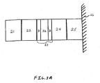
- FIG. 3A is a schematic cross-section of a five layer electrochromic device having an improved ion conductor layer in accordance with one embodiment of the current invention.
- FIG. 3B is a schematic cross-section of a five layer electrochromic device having an improved ion conductor layer, wherein the counter electrode layer and the electrochromic electrode layer are reversed.
- One object of the present invention is to provide an electrochromic device having an improved ion conductor layer.
- the improved ion conductor layer serves to block electron flow in both directions while permitting ionic conduction.
- the improved ion conductor layer also provides thermal stabilization properties, which are desirable for more robust processing.
- This and other objectives are realized by means of an electrochromic device utilizing a multi-layered thin film ion conductor comprised of thin films of at least two ion transport layers and a buffer layer, wherein the at least two ion transport layers and the buffer layer alternate within the ion conducting layer.
- Such a multi-layered thin film ion conductor layer allows for devices to color more deeply by increasing the voltage developed across the ion conductor prior to electronic breakdown while reducing the amount of electronic leakage.
- Another objective of the present invention is to provide an ion conductor layer which may be used in electrochromic devices and in other applications requiring ion conductor layers, such as batteries.
- Yet another objective of the present invention is to provide a method of preparing an electrochromic device comprising an improved ion conducting layer.
- Yet a further objective of the present invention is to provide a method of preparing an improved ion conducting layer for use in electrochromic devices and in other applications requiring ion conductor layers.
- FIG. 3A illustrates a solid-state electrochromic device, in cross-section, having an improved ion conductor layer.
- the device of FIG. 3A is similar to the solid-state device depicted in FIG. 1 to the extent that each of the aforementioned layers is present in the current invention.
- the ion conductor layer of the current invention is comprised of multiple layers, as described herein.
- the device of the present invention has the following thin film layers: an electrochromic electrode layer (“EC") 24 acting as a first electrode which produces a change in absorption or reflection upon oxidation or reduction; an ion conductor layer (“IC") 23 comprised of alternating ion transport and buffer layers which functionally replaces an electrolyte allowing the passage of ions while blocking electronic charge; a counter electrode layer (“CE”) 22 acting as a second electrode which serves as a storage layer for ions when the device is in the bleached state; and two conductive layers (“TC”) 21 and 25 which serve to apply an electrical potential to the electrochromic device.
- EC electrochromic electrode layer
- IC ion conductor layer
- CE counter electrode layer
- TC conductive layers
- the electrochromic device of FIG. 3A is transformed from a substantially transparent state to a less transparent or dark state by application of a positive voltage to the conductive layer 21 relative to the other conductive layer 25.
- the applied voltage causes charge compensating ions, such as lithium, sodium, or hydrogen ions, to pass from the counter electrode layer 22 into the electrochromic electrode layer 24 via the ion conductor layer 23.
- charge compensating ions such as lithium, sodium, or hydrogen ions
- electrons are transported around the external circuit via the transparent conductors 21 and 25, and injected into the electrochromic electrode layer 24.
- the injected electrons yield a reversible electrochemical reduction of the material comprising the electrochromic electrode layer, resulting in reversible changes in the device's intrinsic optical properties, such as optical absorbance and the index of refraction. This overall reversible process is promoted by the simultaneous injection of charge compensating ions into the electrochromic electrode layer.
- the polarity of the circuit is reversed by applying a positive voltage to the transparent conductor 25 relative to the transparent conductor 21. This causes charge compensating ions to flow out of the electrochromic electrode layer, back through the ion conductor layer 23, and into the counter electrode layer 22. Meanwhile, the polarity reversal causes electrons to flow out of the electrochromic electrode layer, around the external circuit, and into the counter electrode layer 22. This extraction of electrons yields a reversible electrochemical oxidation of the material comprising the electrochromic electrode layer, reversing the aforementioned changes in intrinsic optical properties.
- the counter electrode layer 22 and the electrochromic electrode layer 24 may be reversed in the overall structure of FIG. 3A .
- the counter electrode layer acts as the first electrode and the electrochromic electrode layer acts as the second electrode.
- the polarity of the applied potential must be adjusted to ensure that the correct polarity for the layers is maintained.
- the ion conductor layer may be comprised of any number of ion transport and buffer layers provided that: (a) the ion transport and buffer layers alternate within the ion conductor layer; (b) the layer deposited immediately adjacent to the first deposited electrode, either the electrochromic electrode layer or the counter electrode layer, is an ion transport layer; and (c) the layer deposited immediately adjacent to the second deposited electrode, the other of the electrochromic electrode layer or the counter electrode layer, is an ion transport layer.
- the ion transport and buffer layers alternate within the ion conductor layer
- the layer deposited immediately adjacent to the first deposited electrode, either the electrochromic electrode layer or the counter electrode layer is an ion transport layer
- the layer deposited immediately adjacent to the second deposited electrode, the other of the electrochromic electrode layer or the counter electrode layer is an ion transport layer.
- the ion conductor layer is comprised of two ion transport layers 31 and 33, separated by a buffer layer 32, wherein the ion transport layers 31 and 33 are in communication with a counter electrode layer 22 and an electrochromic electrode layer 24, respectively.
- the ion conductor layer is comprised of two ion transport layers and one buffer layer.
- the ion conductor layer is comprised of three ion transport layers and two buffer layers.
- the ion conductor layer is comprised of four ion transport layers and three buffer layers.
- any two adjacent ion transport and buffer layers comprising the ion conductor layer are comprised of different materials.
- the ion transport layer 31 may be comprised of silicon dioxide
- the buffer layer 32 may be comprised of tungsten oxide
- the ion transport layer 33 may be comprised of silicon dioxide.
- a heterogeneous junction is formed at each ion transport and buffer layer interface.
- a heterojunction is an electronic barrier resulting from the difference in bandgap energies of the dissimilar materials constituting adjacent layers. As such, electronic conductivity is blocked in a direction perpendicular to the layers by virtue of this electronic bandgap difference.
- a heterojunction is formed at each ion transport and buffer layer interface or each buffer layer and ion transport interface comprising the ion conductor layer. Heterojunctions are also formed at the ion transport layer and first electrode interface and the ion transport layer and second electrode interface. It is believed that these heterojunctions provide for the enhanced electron blocking of the current invention.
- the materials comprising the ion transport layers are selected from insulators. When used in window applications, such as architectural windows, it is preferred that the ion conductor be selected from a transparent insulator.
- transparent means that a significant percentage of incident light intensity may be transmitted through a thin film over a wide angular range of incidence. The percentage of transmission of incident light intensity may range from less than about 20% transmittance to greater than about 80% transmittance, depending on the specific application, with the non-transmitted light intensity lost to physical processes including optical absorption, light scattering, and optical reflection.
- the magnitude of light intensity loss depends upon both the thickness of the insulator material and the insulator material's intrinsic optical properties, including optical absorptivity, the concentration of light absorbing species, the concentration and cross section of light scattering centers, and the refractive index with respect to adjoining materials. It will be appreciated that both the thickness and intrinsic optical properties of the insulator material may be selected to suit certain applications. For example, in architectural window applications, the percent transmission needs to be optimized but not necessarily maximized. In this case, a significant loss of incident light intensity may be desired. On the other hand, in certain electronic display applications, the light scattering and optical absorption of the insulator material may both need to be maximized to provide a substantially opaque backdrop for the reversibly coloring electrochromic material. It can further be appreciated that the selection and combination of ion transport layers comprised of various insulator materials affords several optical degrees of freedom over which optical transmission, reflection and light scattering can be optimized.
- the insulators of the current invention are characterized by a full valence band separated from an empty conduction band by a few electron volts.
- electronic conduction cannot take place in either the filled or empty bands unless additional carriers (i.e. electrons or holes) are introduced.
- additional carriers i.e. electrons or holes
- the ionic conductivity of such insulator materials is unrelated to the band structure, depending instead on the physical structure of the material itself.
- the simplest electronic conduction mechanism is the direct quantum-mechanical tunneling of electrons or holes from a first to a second electrode.
- the carriers may also be injected into the conduction or valence band of the insulator by thermionic or Schottky emission over the metal-insulator interface barrier. Moreover, the carriers may tunnel through the insulator barrier gap at high fields (field or cold emission).
- Transport of carriers in the conduction band is modulated by scattering processes. While it is believed that lattice scattering is not expected to be significant for the thin layers of the current invention, it should be noted that less ordered films (such as amorphous films) contain a large number of traps. In the presence of such traps, conduction can also take place by tunneling between traps, or depending on the type of traps, by hopping from trap to trap (see Kasturi L. Chopra's Thin Film Phenomena, McGraw Hill: 1969, pages 479 and following, incorporated herein by reference).
- Insulators which may be utilized as part of the current invention include, but are not limited to, silicon oxides, aluminum oxides, aluminum nitrides, niobium oxides, tantalum oxides, titantium oxides, zirconium oxides, yttrium oxides, hafnium oxides, and mixtures thereof.
- Specific insulators which may be utilized include, but are not limited to, SiO 2 , Al 2 O 3 , Nb 2 O 3 , Ta 2 O 5 , LiTaO 3 , LiNbO 3 , La 2 TiO 7 , La 2 TiO 7 , SrZrO 3 , ZrO 2 , Y 2 O 3 , Nb 2 O 5 , La 2 Ti 2 O 7 , LaTiO 3 , HfO 2 and mixtures thereof.
- Specific mixtures which may be utilized include mixtures of SiO 2 and Al 2 O 3 and mixtures of ZrO 2 and Y 2 O 3 . If a mixture of any two materials is utilized, the amount of the first material to the amount of the second material ranges from about 30:1 to 1:30, preferably from about 20:1 to about 1:20.
- the materials comprising the ion transport layers are selected from SiO 2 , Al 2 O 3 , and Nb 2 O 3 .
- the ion transport layer is a mixture of a silicon oxide and aluminum oxide, wherein the ratio of silicon oxide to aluminum oxide in such a mixture ranges from about 25:1 to about 1:25, preferably the ratio of silicon oxide to aluminum oxide ranges from about 11:1 to about 17:1.
- any of the materials selected for use in the ion transport layers may be mixed with one or more additives selected from metals, metal oxides, compounds containing metals, molecules, or atomic species to alter the chemical and/or physical properties of one or more ion transport layers.
- each ion transport layer comprising the ion conductor is comprised of the same material.
- some of the ion transport layers comprising the ion conduction may be comprised of one type of material while other ion transport layers comprising the same ion conductor may be comprised of a different type of material. Indeed, it is possible for each of the ion transport layers comprising the ion conductor layer to be made from different materials.
- the thickness of the ion transport layer varies depending on the material comprising the layer and the desired properties of the electrochromic device. However, the ion transport layer typically ranges from about 1 nm to about 70 nm in thickness, preferably from about 5 nm to about 30 nm in thickness. Each ion transport layer comprising the ion conductor layer may be about the same thickness or may be of varied thicknesses. It is preferred, however, that each of the ion transport layers be about the same thickness. Moreover, the ion transport layers may be of the same or different thicknesses as compared with the buffer layers.
- any material may be used as a buffer layer provided it allows for the passage of ions from one ion transport layer to another.
- the material comprising the buffer layer has low or no electronic conductivity, but this is not essential.
- the buffer layers are selected from materials including transparent lithium ion permeable materials and mixed conductors. As used herein, a "mixed conductor" means an ion/electron conductor.
- the buffer layer comprises metal oxides including, but not limited to, tungsten oxides, nickel oxides, cerium oxides, molybdenum oxides, vanadium oxides, and mixtures thereof.
- Specific buffer layer materials include, but are not limited to, WO 3 , NiO, CeO 2 , MoO 3 , V 2 O 5 , and mixtures thereof.
- Specific mixtures which may be utilized include mixtures of NiO and WO 3 , mixtures of CeO 2 and MoO 3 , mixtures of CeO 2 and V 2 O 5 , mixtures of MoO 3 and V 2 O 5 , and mixtures of CeO 2 , MoO 3 , and V 2 O 5 . If a mixture of any two materials is utilized, the amount of the first material to the amount of the second material ranges from about 30:1 to about 1:30, preferably from about 20:1 to about 1:20.
- the buffer layer comprises a silica-based, an alumina-based, or an alumina-silica-based structure.
- Other buffer materials particularly adapted for lithium ion transmission are lithium-based ceramic materials including lithium silicates, lithium aluminum silicates, lithium aluminum borates, lithium borates, lithium silicon oxynitrides, lithium zirconium silicates, lithium niobates, lithium borosilicates, lithium phosphosilicates, lithium nitrides, lithium aluminum fluoride, and other lithium-based ceramic materials, silicas, or silicon oxides.
- the buffer layer is selected from the group consisting of tungsten oxide and mixtures of nickel oxide and tungsten oxide.
- each buffer layer comprised in the ion conductor layer is comprised of the same material. In other embodiments, however, some of the buffer layers comprised in the ion conductor layer may be comprised of one type of material while other buffer layers comprising the same ion conductor layer may be comprised of a different type of material. Indeed, it is possible for each of the buffer layers comprised in the ion conductor to be made from different materials.
- the thickness of the buffer layer varies depending on the material comprising the layer and the desired properties of the electrochromic electrode layer device. However, the buffer layer typically ranges from about 10 nm to about 300 nm in thickness, preferably from about 30 nm to about 150 nm in thickness. Each buffer layer comprising the ion conductor layer may be about the same thickness or may be of varied thicknesses. It is preferred, however, that the buffer layers be about the same thickness. Moreover, the buffer layers may be of the same or different thicknesses as compared with the ion transport layers.
- the ion conductor layer is comprised of a silicon dioxide first ion transport layer, a tungsten oxide buffer layer, and a second silicon dioxide ion transport layer.
- the ion conductor layer is comprised of a silicon dioxide first ion transport layer, a niobium oxide buffer layer, and a silicon dioxide second ion transport layer.
- the ion conductor layer is comprised of a silicon oxide/aluminum oxide first ion transport layer, a tungsten oxide buffer layer, and a silicon oxide/aluminum oxide second ion transport layer.
- the ion conductor layer is comprised of a silicon dioxide first ion transport layer, a tungsten oxide first buffer layer, a silicon dioxide second ion transport layer, a tungsten oxide second buffer layer, and a silicon dioxide third ion transport layer.
- the overall thickness of the ion conductor layer depends upon how many ion transport and buffer layers comprise the ion conductor layer, the materials comprising each of those layers, and the thicknesses of each of those layers.
- the electrochromic devices of the present invention comprise a counter electrode layer 22 in communication with one of the ion transport layers.
- the purpose of the counter electrode layer is primarily to "insert" and store the charge compensating ions, such as lithium, sodium, or hydrogen ions, when not employed in the electrochromic electrode layer.
- Some counterelectrode materials are also electrochromic in that they change their shade or transparency as ions move in or out. Such materials can complement the coloration of the electrochromic layer.
- the counter electrode layer 22 is typically formed from a material which is capable of storing ions and then releasing these ions for transmission to the electrochromic electrode layer 24 in response to an appropriate electric potential.
- the counter electrode layer is comprised of a metal oxide including the oxides of vanadium, niobium, nickel, iridium, cobalt, tungsten, tantalum and molybdenum.
- Preferred metal oxide materials for the counter electrode layer include vanadium pentoxide, niobium oxide, nickel oxide, nickel hydroxide, iridium oxide, cobalt oxide, molybdenum oxide, and mixtures (both intercalated and chemically combined forms) of these materials, such as chromium vanadium oxide, tungsten-nickel oxide, tantalum-nickel oxide and the like.
- the counter electrode layer is comprised of a mixed metal oxide comprising a first transition metal oxide present as a stable metal oxide matrix and a second transition metal doped into the stable metal oxide matrix.
- the first transition metal is selected from chromium, tungsten, and tantalum.
- the second transition metal is selected from vanadium and nickel.
- the current invention also contemplates the lithium doped compounds of each of the aforementioned metal oxides.
- the thickness of the counter electrode layer 22 varies depending on the application sought for the electrochromic device, the transmission range desired, and the material comprising the counter electrode layer. As such, the thickness may range from about 50 nm to about 650 nm. In one embodiment of the present invention, the thickness may range from about 150 nm to about 250 nm, preferably ranging from about 175 nm to about 205 nm in thickness.
- the electrochromic devices of the present invention also comprise an electrochromic electrode layer 22 in communication with another of the ion transport layers.
- the materials constituting the electrochromic electrode layer 24 are well known in the art and include inorganic materials, organic materials, and/or composites of inorganic and organic electrochemically active materials such that the electrochromic electrode layer is capable of receiving ions transferred from the CE layer 22.
- Exemplary electrochemically active inorganic metal oxides include WO 3 , V 2 O 5 , MoO 3 , Nb 2 O 5 , TiO 2 , CuO, Ni 2 O 3 , Ir 2 O 3 , Cr 2 O 3 , Co 2 O 3 , Mn 2 O 3 , mixed oxides (e.g W-Mo oxide, W-V oxide) and the like.
- Electrochromic electrode layer of the current invention examples include those enumerated in C.G.Granvist, Handbook of Inorganic Electrochromic Materials, 1995: Elsevier , incorporated herein by reference.
- metal oxides may be appropriately mixed with metals including lithium, sodium, potassium, molybdenum, vanadium, titanium, and/or other suitable metals, compounds, or molecules containing metals.
- the EC layer 24 is selected from tungsten oxide or tungsten oxide doped with another metal or metal containing molecule.
- the thickness of the electrochromic electrode layer 24 varies depending on the electrochemically active material chosen. However, the EC layer 24 typically ranges from about 50 nm to about 550 nm in thickness, preferably from about 300 nm to about 450 nm.
- conductive layer materials include coatings of indium oxide, indium tin oxide, doped indium oxide, tin oxide, doped tin oxide, zinc oxide, doped zinc oxide, ruthenium oxide, doped ruthenium oxide and the like, as well as all thin metallic coatings that are substantially transparent, comprised of metals including gold, silver, aluminum, nickel alloy, and the like. It is also possible to employ multiple layer coatings, such as those available from Pilkington under the trade name of TEC-Glass®, or those available from PPG Industries under the trade names SUNGATE® 300 and SUNGATE® 500.
- the conductive layers 21 and 25 may also be composite conductors prepared by placing highly conductive ceramic and metal wires or conductive layer patterns on one of the faces of the substrate and then over coating this with transparent conductive materials such as indium tin oxide or doped tin oxides.
- the conductive layers may be further treated with appropriate anti-reflective or protective oxide or nitride layers.
- the conductive layers utilized in the present invention are transparent layers of indium tin oxide.
- the material selected for use in conductive layer 25 is the same as the material selected for use in conductive layer 21. In other embodiments, the material selected for use in conductive layer 25 is different than the material selected for use in conductive layer 21.
- the conductive layer 25 is disposed on a substrate 26 having suitable optical, electrical, thermal, and mechanical properties such as, for example, glass, plastic or mirror materials, as a coating having a thickness in the range of about 5 nm to about 10,000 nm, preferably in the range of about 10 nm to about 1,000 nm.
- suitable optical, electrical, thermal, and mechanical properties such as, for example, glass, plastic or mirror materials
- any thickness of the conductive layer may be employed that provides adequate conductance for the electrochromic device and which does not appreciably interfere with the transmission of light where required.
- conductive layer 21 is typically the final layer of the electrochromic device deposited on the counter electrode layer 22.
- Other passive layers used for improving optical properties, or providing moisture or scratch resistance may be deposited on top of the active layers. These conductive layers are connected to an electrical power source in a conventional manner.
- the substrate 26 of the electrochromic device is comprised of transparent glass or plastic such as, for example, acrylic, polystyrene, polycarbonate, allyl diglycol carbonate, styrene acrylonitrile copolymer, poly(4-methyl-1-pentene), polyester, polyamide, etc.
- transparent glass or plastic such as, for example, acrylic, polystyrene, polycarbonate, allyl diglycol carbonate, styrene acrylonitrile copolymer, poly(4-methyl-1-pentene), polyester, polyamide, etc.
- the transparent substrate 26 is either clear or tinted soda lime glass, preferably float glass, in which case a sodium ion diffusion barrier is typically applied to the bare substrate before depositing any of the layers described above.
- the sodium diffusion barrier prevents sodium ions from migrating from the bulk of the glass substrate into the overlying films, especially the first conductive layer and the electrochromic layer, during thermal processing.
- plastic it is preferably abrasion protected and barrier protected using a hard coat of, for example, a silica/silicone anti-abrasion coating, a diamond-like protection coating or the like, such as is known in the plastic glazing art.
- the substrates have a thickness in the range of about 0.01 mm to about 10 mm, and preferably in the range from about 0.1 mm to 5 mm. However, any substrate of any thickness which will provide a functioning electrochromic device may be employed.
- an electrochromic device employing two ion transport layers is: a bottom conductive layer, a tungsten oxide electrochromic electrode layer, a silicon oxide first ion transport layer, a tungsten oxide buffer layer, a second silicon oxide layer, a nickel oxide counter electrode layer, and a top conductive layer.
- Another example of an electrochomic device having two ion transport layers is: a bottom conductive layer, a tungsten oxide electrochromic electrode layer, a silicon oxide first ion transport layer, a niobium oxide buffer layer, a silicon oxide second ion transport layer, a nickel oxide counter electrode layer, and a top conductive layer.
- An example of an electrochromic device having three ion transport layers is: a bottom conductive layer, a tungsten oxide electrochromic electrode layer, a silicon oxide first ion transport layer, a tungsten oxide first buffer layer, a silicon oxide second ion transport layer, a tungsten oxide second buffer layer, a third silicon oxide ion transport layer, a nickel oxide counter electrode layer, and a top conductive layer.
- the electrochromic device of the present invention may be powered with alternate electrical sources including solar cells, thermoelectric sources, wind generators, etc., to make them self-sustaining. These may be also coupled into charge storage devices such as batteries, re-chargeable batteries, capacitors or other means.
- the electrochromic device of the present invention may also be used as filters in displays or monitors for reducing the ambient light intensity, e.g., sun glare, that is incident on the monitor or display surface.
- the device may be employed to enhance the image quality of displays and monitors, particularly in well lit conditions.
- the ion conductor layer as described herein may be used in any other application or electrochromic device where an ion conductor layer is needed, such as in batteries. That is, the ion conductor layer is not limited to use in the specific electrochromic device described herein.
- the sequence of deposition steps, the number of deposition layers, and the composition or type of layers which are deposited may be varied to achieve the desired results without departing from the teachings of the present invention.
- a bottom conductive layer is deposited on a substrate.
- the bottom conductive layer may be deposited by any techniques known in the art including wet chemical methods, chemical vapor deposition, or physical vapor deposition processes.
- the materials comprising a conductor layer are deposited via sputtering onto a transparent substrate to form a first transparent conductor layer.
- a first electrode is then deposited on the bottom transparent conductor layer through wet chemical methods, chemical vapor deposition, or physical vapor deposition.
- Preferred methods of deposition include sol-gel, spray pyrolysis, electrodeposition, metallo-organic decomposition, laser ablation, pulsed laser ablation, evaporation, e-beam assisted evaporation, sputtering, intermediate frequency reactive sputtering, RF sputtering, magnetic sputtering, DC sputtering, reactive DC magnetron sputtering and the like.
- the first electrode is deposited via intermediate frequency reactive sputtering or DC sputtering techniques. In some embodiments, the first electrode layer is deposited on a heated bottom transparent conductor layer.
- the individual ion transport and buffer layers comprising the ion conductor layer are then sequentially deposited on the first deposited electrode.
- Any number of ion transport and buffer layers may be deposited on the electrochromic electrode layer provided that: a) the ion transport and buffer layers alternate within the ion conductor layer; b) the layer deposited immediately adjacent to the first deposited electrode, either the electrochromic electrode or the counter electrode, is an ion transport layer; and c) the layer deposited immediately adjacent to the second deposited electrode, the other of the electrochromic electrode or the counter electrode, is an ion transport layer.
- the ion transport and buffer layers may be comprised of the materials discussed herein. In preferred embodiments, adjacent ones of the ion transport layers and buffer layer are comprised of different materials.
- Each ion transport layer and/or buffer layer may be deposited via the same deposition process or may be deposited via different processes.
- the individual ion transport and buffer layers may be sequentially deposited by wet chemical methods, chemical vapor deposition or physical vapor deposition.
- Such methods of deposition include sol-gel, metallo-organic decomposition, laser ablation, evaporation, e-beam assisted evaporation, sputtering, intermediate frequency reactive sputtering, RF sputtering, magnetic sputtering, DC sputtering, and the like.
- the ion transport and buffer layers are each independently deposited by intermediate frequency reactive sputtering or DC sputtering techniques.
- the ion transport and buffer layers are each deposited by sol-gel thin film deposition techniques including dip coating, spin coating and spray coating.
- some of the ion transport layers or buffers are deposited by sputtering while other ion transport or buffer layers are deposited by sol-gel techniques. The procedures for depositing such layers by sputtering or sol-gel coating are known to those skilled in the art.
- Preferred methods of deposition include sol-gel techniques, spray pyrolysis, electrodeposition, metallo-organic decomposition, laser ablation, pulsed laser ablation, evaporation, e-beam assisted evaporation, sputtering, intermediate frequency reactive sputtering, RF sputtering, magnetic sputtering, DC sputtering, reactive DC magnetron sputtering and the like.
- a second conductive layer 21 is deposited on the counter electrode layer 22 by methods well known in the art and as described above in the deposition of the first conductive layer 25.
- charge compensating ions such as protons (H+), lithium ions, or sodium ions
- intercalation means the reversible insertion of a molecule, atom or ion into the lattice of an electrochromic device layer.
- the charge compensating ion is lithium, wherein the lithium ions are deposited by magnetron sputter deposition of atomic lithium from a metallic sputter target into the device, under vacuum processing conditions.
- the intercalation step occurs after the deposition of one or both of the electrode layers.
- the intercalation step may occur after the deposition of any layer of the electrochromic device.
- the amount of charge compensating ion deposited is carefully controlled such that an amount of charge compensating ion is added that allows for the greatest transmission of light through the electrochromic device.
- the device may optionally be heat treated by heating the electrochromic device.
- the heat treatment process is carried out subsequent to fabrication of the device, i.e. after the electrochromic layers have been deposited and at least one of the electrochromic layer and/or counterelectrode layers has been reduced via intercalation of charge compensating ions, as discussed above. Carrying out the heat treatment process at this point improves the switching characteristics of the electrochromic devices. Moreover, it is believed that the heat treatment process improves the conductivity and transparency of the device, especially the transparent conductor layers. Further, it is believed that the improved ion conductor of the current invention acts as a thermal stabilization layer which helps stabilize the integrity of the interfaces during any heat treatment process.
- the heat treatment process may occur in a vacuum, an inert atmosphere, or an atmospheric oven.
- the treatment itself typically occurs at temperatures ranging from about 40°C to about 550°C, preferably ranging from about 200°C to about 500°C.
- the electrochromic device is placed in an oven at room temperature and then heat is applied.
- the electrochromic device is placed in a pre-heated oven.
- the device may be heated for a time ranging from about 1 minute to about 120 minutes, preferably ranging from about 10 minutes to about 30 minutes.
- the temperature is ramped as the heat treatment process progresses.
- the device can be heated prior to the deposition of the second transparent conductor. This method results in electrochromic device whose properties are similar to those discussed in the preceding embodiment, but allows for the heating to be done in the same process chamber as the deposition, resulting in improved process flow.
- the position of the counter electrode layer 22 and the electrochromic layer 24 may be reversed in the overall structure presented in FIG. 3 .
- the method of manufacturing the device does not change with regard to the steps that must be performed to generate each layer.
- the methods utilized above to create the improved ion conductor layer of the present invention may be used to develop an ion conductor for use in connection with any electrochromic device or any other application requiring ion conductor layers, such as batteries. That is, the methods used to develop the ion conductor layer are not limited to use in the specific electrochromic device discussed herein. Moreover, the method of making the improved ion conductor discussed above may also be used to deposit an improved ion conductor on any surface or substrate, including, but not limited to, electrodes or conductive thin films.
Landscapes
- Physics & Mathematics (AREA)
- Chemical & Material Sciences (AREA)
- Nonlinear Science (AREA)
- Chemical Kinetics & Catalysis (AREA)
- Electrochemistry (AREA)
- Inorganic Chemistry (AREA)
- General Physics & Mathematics (AREA)
- Optics & Photonics (AREA)
- Electrochromic Elements, Electrophoresis, Or Variable Reflection Or Absorption Elements (AREA)
Applications Claiming Priority (2)
| Application Number | Priority Date | Filing Date | Title |
|---|---|---|---|
| US72558105P | 2005-10-11 | 2005-10-11 | |
| EP06021342A EP1775625A3 (de) | 2005-10-11 | 2006-10-11 | Elektrochrome Vorrichtungen mit verbesserten ionenleitenden Schichten |
Related Parent Applications (1)
| Application Number | Title | Priority Date | Filing Date |
|---|---|---|---|
| EP06021342.8 Division | 2006-10-11 |
Publications (1)
| Publication Number | Publication Date |
|---|---|
| EP2290438A1 true EP2290438A1 (de) | 2011-03-02 |
Family
ID=37684157
Family Applications (2)
| Application Number | Title | Priority Date | Filing Date |
|---|---|---|---|
| EP10011284A Withdrawn EP2290438A1 (de) | 2005-10-11 | 2006-10-11 | Elektrochrome Vorrichtungen mit verbesserten ionenleitenden Schichten |
| EP06021342A Withdrawn EP1775625A3 (de) | 2005-10-11 | 2006-10-11 | Elektrochrome Vorrichtungen mit verbesserten ionenleitenden Schichten |
Family Applications After (1)
| Application Number | Title | Priority Date | Filing Date |
|---|---|---|---|
| EP06021342A Withdrawn EP1775625A3 (de) | 2005-10-11 | 2006-10-11 | Elektrochrome Vorrichtungen mit verbesserten ionenleitenden Schichten |
Country Status (3)
| Country | Link |
|---|---|
| US (3) | US7593154B2 (de) |
| EP (2) | EP2290438A1 (de) |
| JP (1) | JP5420818B2 (de) |
Families Citing this family (143)
| Publication number | Priority date | Publication date | Assignee | Title |
|---|---|---|---|---|
| US7684786B2 (en) * | 2003-08-26 | 2010-03-23 | Nokia Corporation | Method and system for establishing a connection between network elements |
| CN101584065B (zh) | 2007-01-12 | 2013-07-10 | 易诺维公司 | 三维电池及其制造方法 |
| US7808693B2 (en) * | 2007-06-07 | 2010-10-05 | Soladigm, Inc. | Electrochromic devices and fabrication methods |
| US7609433B2 (en) * | 2007-06-07 | 2009-10-27 | Soladigm, Inc. | Electrochromic device and method of making the same |
| US8115984B2 (en) * | 2007-06-18 | 2012-02-14 | Ajjer Llc | Laminated electrochromic devices and processes for forming the same |
| US8988756B2 (en) * | 2008-01-31 | 2015-03-24 | Ajjer, Llc | Conductive busbars and sealants for chromogenic devices |
| US9782949B2 (en) | 2008-05-30 | 2017-10-10 | Corning Incorporated | Glass laminated articles and layered articles |
| US8842357B2 (en) * | 2008-12-31 | 2014-09-23 | View, Inc. | Electrochromic device and method for making electrochromic device |
| US8582193B2 (en) | 2010-04-30 | 2013-11-12 | View, Inc. | Electrochromic devices |
| US9007674B2 (en) | 2011-09-30 | 2015-04-14 | View, Inc. | Defect-mitigation layers in electrochromic devices |
| US12043890B2 (en) | 2009-03-31 | 2024-07-23 | View, Inc. | Electrochromic devices |
| US10261381B2 (en) | 2009-03-31 | 2019-04-16 | View, Inc. | Fabrication of low defectivity electrochromic devices |
| WO2016085764A1 (en) | 2014-11-26 | 2016-06-02 | View, Inc. | Counter electrode for electrochromic devices |
| US10591795B2 (en) | 2009-03-31 | 2020-03-17 | View, Inc. | Counter electrode for electrochromic devices |
| US8300298B2 (en) | 2010-04-30 | 2012-10-30 | Soladigm, Inc. | Electrochromic devices |
| US8432603B2 (en) * | 2009-03-31 | 2013-04-30 | View, Inc. | Electrochromic devices |
| US9261751B2 (en) | 2010-04-30 | 2016-02-16 | View, Inc. | Electrochromic devices |
| US8764950B2 (en) | 2010-04-30 | 2014-07-01 | View, Inc. | Electrochromic devices |
| WO2016085823A1 (en) * | 2014-11-26 | 2016-06-02 | View, Inc. | Counter electrode for electrochromic devices |
| US10852613B2 (en) | 2009-03-31 | 2020-12-01 | View, Inc. | Counter electrode material for electrochromic devices |
| US10156762B2 (en) | 2009-03-31 | 2018-12-18 | View, Inc. | Counter electrode for electrochromic devices |
| US8764951B2 (en) | 2010-04-30 | 2014-07-01 | View, Inc. | Electrochromic devices |
| US11599003B2 (en) | 2011-09-30 | 2023-03-07 | View, Inc. | Fabrication of electrochromic devices |
| US11187954B2 (en) | 2009-03-31 | 2021-11-30 | View, Inc. | Electrochromic cathode materials |
| GB2469285A (en) * | 2009-04-06 | 2010-10-13 | Ntnu Technology Transfer As | Ferroelectric niobate materials formed by spray pyrolysis |
| US8482837B2 (en) | 2010-03-05 | 2013-07-09 | Sage Electrochromics, Inc. | Lamination of electrochromic device to glass substrates |
| US8493646B2 (en) | 2010-04-22 | 2013-07-23 | Sage Electrochromics, Inc. | Series connected electrochromic devices |
| US8228587B2 (en) | 2010-04-22 | 2012-07-24 | Sage Electrochromics, Inc. | Series connected electrochromic devices |
| US9759975B2 (en) | 2010-04-30 | 2017-09-12 | View, Inc. | Electrochromic devices |
| FR2962682B1 (fr) | 2010-07-16 | 2015-02-27 | Saint Gobain | Vitrage electrochimique a proprietes optiques et/ou energetiques electrocommandables |
| US9843027B1 (en) | 2010-09-14 | 2017-12-12 | Enovix Corporation | Battery cell having package anode plate in contact with a plurality of dies |
| US8164818B2 (en) | 2010-11-08 | 2012-04-24 | Soladigm, Inc. | Electrochromic window fabrication methods |
| KR20140017595A (ko) | 2011-03-31 | 2014-02-11 | 세이지 일렉트로크로믹스, 인크. | 열 이미징을 사용하여 전기발색 디바이스에서 결함을 검출하고 보수하는 시스템 및 방법 |
| US8430707B2 (en) | 2011-05-27 | 2013-04-30 | Sage Electrochromics, Inc. | Apparatus and method for repair of defects in an electronic energy control or display device |
| WO2013003458A1 (en) | 2011-06-27 | 2013-01-03 | Soleras Ltd. | Sputtering target |
| US9217198B2 (en) | 2011-07-07 | 2015-12-22 | Itn Energy Systems, Inc. | Insertion of lithium into electrochromic devices after completion |
| US9885934B2 (en) | 2011-09-14 | 2018-02-06 | View, Inc. | Portable defect mitigators for electrochromic windows |
| EP2756289B1 (de) | 2011-09-14 | 2023-03-29 | View, Inc. | Tragbarer fehlerreduzierer für elektrochrome fenster |
| TR201905334T4 (tr) | 2011-10-10 | 2019-05-21 | Saint Gobain | Kapasitif sensör devre yüzeyli elektrokromatik yalıtıcı camlama. |
| WO2013074702A1 (en) | 2011-11-15 | 2013-05-23 | Ashwin-Ushas Corporation, Inc. | Complimentary polymer electrochromic device |
| US9777365B2 (en) | 2011-11-29 | 2017-10-03 | Itn Energy Systems, Inc. | Multi-zone modular coater |
| US10606142B2 (en) | 2011-12-12 | 2020-03-31 | View, Inc. | Thin-film devices and fabrication |
| US10739658B2 (en) | 2011-12-12 | 2020-08-11 | View, Inc. | Electrochromic laminates |
| US11048137B2 (en) | 2011-12-12 | 2021-06-29 | View, Inc. | Thin-film devices and fabrication |
| US10802371B2 (en) | 2011-12-12 | 2020-10-13 | View, Inc. | Thin-film devices and fabrication |
| US12061402B2 (en) | 2011-12-12 | 2024-08-13 | View, Inc. | Narrow pre-deposition laser deletion |
| CN104011588B (zh) | 2011-12-12 | 2021-06-22 | 唯景公司 | 薄膜装置和制造 |
| US9293796B2 (en) | 2011-12-15 | 2016-03-22 | Itn Energy Systems, Inc. | Metal-air battery with dual electrode anode |
| US8980485B2 (en) | 2011-12-30 | 2015-03-17 | Itn Energy Systems, Inc. | Rechargeable, thin-film, all solid-state metal-air battery |
| US9281672B2 (en) | 2012-01-20 | 2016-03-08 | Sage Electrochromics, Inc. | Electrical connectivity within architectural glazing frame systems |
| EP2807698B1 (de) * | 2012-01-24 | 2018-01-10 | Enovix Corporation | Ionisch durchlässige strukturen für energiespeichereinrichtungen |
| US8976440B2 (en) | 2012-02-03 | 2015-03-10 | Itn Energy Systems, Inc. | Autonomous electrochromic assembly |
| US9013777B2 (en) | 2012-02-03 | 2015-04-21 | Itn Energy Systems, Inc. | Integrated device architectures for electrochromic devices |
| US20130222877A1 (en) | 2012-02-28 | 2013-08-29 | Sage Electrochromics, Inc. | Multi-zone electrochromic devices |
| US20130222878A1 (en) | 2012-02-28 | 2013-08-29 | Sage Electrochromics, Inc. | Multi-zone electrochromic devices |
| US9341912B2 (en) | 2012-03-13 | 2016-05-17 | View, Inc. | Multi-zone EC windows |
| EP4134733A1 (de) | 2012-03-13 | 2023-02-15 | View, Inc. | Stiftlochabschwächung für optische vorrichtungen |
| US20130258436A1 (en) | 2012-04-03 | 2013-10-03 | Sage Electrochromics, Inc. | Patterned obscuration lines for electrochromic devices |
| IN2014DN08858A (de) | 2012-04-05 | 2015-05-22 | Sage Electrochromics Inc | |
| WO2013158888A1 (en) * | 2012-04-18 | 2013-10-24 | Applied Materials, Inc. | Pinhole-free solid state electrolyte with high ionic conductivity |
| CN104302437B (zh) | 2012-05-18 | 2017-09-05 | 唯景公司 | 限制光学装置中的缺陷 |
| EP2867430A1 (de) | 2012-06-27 | 2015-05-06 | Sage Electrochromics, Inc. | Schulterabstandshalterschlüssel für isolierverglasungen |
| US8995041B2 (en) * | 2012-08-09 | 2015-03-31 | Sage Electrochromics, Inc. | Ternary nickel oxide materials for electrochromic devices |
| JP6416765B2 (ja) | 2012-08-16 | 2018-10-31 | エノビクス・コーポレイションEnovix Corporation | 3次元電池のための電極構造体 |
| EP3054347B1 (de) | 2012-12-28 | 2020-05-20 | e-Vision Smart Optics Inc. | Doppelschichtige elektrode für eine elektrooptische flüssigkristalllinse |
| US9013778B2 (en) | 2013-03-06 | 2015-04-21 | Sage Electrochromics, Inc. | Laser cuts to reduce electrical leakage |
| WO2014137378A1 (en) | 2013-03-08 | 2014-09-12 | Sage Electrochromics, Inc. | Electrochromic device with multiple independently controllable zones and internal busbars |
| WO2014143011A1 (en) * | 2013-03-15 | 2014-09-18 | Ashwin-Ushas Corporation, Inc. | Variable-emittance electrochromic devices and methods of preparing the same |
| WO2014151202A1 (en) | 2013-03-15 | 2014-09-25 | Enovix Corporation | Separators for three-dimensional batteries |
| US9207515B2 (en) | 2013-03-15 | 2015-12-08 | Ashwin-Ushas Corporation, Inc. | Variable-emittance electrochromic devices and methods of preparing the same |
| US9581741B1 (en) | 2013-05-31 | 2017-02-28 | Itn Energy Systems, Inc. | Infrared control coating of thin film devices |
| KR102521229B1 (ko) * | 2013-06-12 | 2023-04-12 | 뷰, 인크. | 개선형 전기 접촉부를 위한 투명 전도 옥사이드(tco) 박막 전처리 |
| US9152001B2 (en) | 2013-07-25 | 2015-10-06 | Sage Electrochromics, Inc. | Electrochromic devices having improved structure for reducing current leakage across lower transparent conductor layers |
| JP2016527559A (ja) * | 2013-07-25 | 2016-09-08 | 三井化学株式会社 | エレクトロクロミック膜及び関連するその製造方法 |
| US9606409B2 (en) | 2013-09-13 | 2017-03-28 | Itn Energy Systems Inc. | Electrochromic window insert assembly and methods of manufacture |
| US8902486B1 (en) | 2013-11-20 | 2014-12-02 | Ashwin-Ushas Corporation, Inc. | Method and apparatus for control of electrochromic devices |
| US20150153622A1 (en) * | 2013-12-03 | 2015-06-04 | Sage Electrochromics, Inc. | Methods for producing lower electrical isolation in electrochromic films |
| US10044028B1 (en) | 2014-01-29 | 2018-08-07 | Itn Energy Systems, Inc. | Composite cathode solid state battery |
| US10767143B2 (en) | 2014-03-06 | 2020-09-08 | Sage Electrochromics, Inc. | Particle removal from electrochromic films using non-aqueous fluids |
| CN104102060A (zh) * | 2014-03-28 | 2014-10-15 | 能源X控股有限公司 | 一种智能变色窗制备方法 |
| US11891327B2 (en) | 2014-05-02 | 2024-02-06 | View, Inc. | Fabrication of low defectivity electrochromic devices |
| US10670936B2 (en) | 2014-07-23 | 2020-06-02 | Kinestral Technologies, Inc. | Wet-coating of thin film lithium nickel oxides for electrochromic applications |
| US10061177B2 (en) | 2014-07-23 | 2018-08-28 | Kinestral Technologies, Inc. | Process for preparing multi-layer electrochromic stacks |
| EP3982195A1 (de) | 2014-09-05 | 2022-04-13 | View, Inc. | Gegenelektrode für elektrochrome vorrichtungen |
| TWI550331B (zh) * | 2014-10-24 | 2016-09-21 | 行政院原子能委員會核能研究所 | 一種全固態電致變色元件的製造方法 |
| WO2018039080A1 (en) | 2016-08-22 | 2018-03-01 | View, Inc. | Electromagnetic-shielding electrochromic windows |
| KR20230014842A (ko) | 2014-12-19 | 2023-01-30 | 뷰, 인크. | 부스 바 하에 있는 전기변색 디바이스에서의 결함들을 완화시키는 방법 |
| FR3031197B1 (fr) * | 2014-12-31 | 2017-06-16 | Saint Gobain | Procede de traitement thermique rapide d'un empilement electrochrome tout solide complet |
| WO2016126460A2 (en) * | 2015-02-06 | 2016-08-11 | Proteq Technologies Llc | Electrochromic devices |
| CA2980477A1 (en) | 2015-03-20 | 2016-09-29 | View, Inc. | Faster switching low-defect electrochromic windows |
| EP3828976B1 (de) | 2015-05-14 | 2023-07-05 | Enovix Corporation | Längsbeschränkungen für energiespeichervorrichtungen |
| US9632059B2 (en) | 2015-09-03 | 2017-04-25 | Ashwin-Ushas Corporation, Inc. | Potentiostat/galvanostat with digital interface |
| US9482880B1 (en) | 2015-09-15 | 2016-11-01 | Ashwin-Ushas Corporation, Inc. | Electrochromic eyewear |
| TWI832314B (zh) | 2016-05-13 | 2024-02-11 | 美商易諾維公司 | 用於三維電池之尺寸拘束件 |
| US11623433B2 (en) | 2016-06-17 | 2023-04-11 | View, Inc. | Mitigating defects in an electrochromic device under a bus bar |
| US9942432B2 (en) | 2016-08-18 | 2018-04-10 | Xerox Corporation | Electrochromic scanning backing material |
| US10900277B1 (en) * | 2016-10-24 | 2021-01-26 | Heliotrope Technologies, Inc. | Monolithic electrochromic window manufacturing methods |
| TWI819481B (zh) | 2016-11-16 | 2023-10-21 | 美商易諾維公司 | 具有可壓縮陰極之三維電池 |
| US11500258B2 (en) | 2016-12-22 | 2022-11-15 | Sage Electrochromics, Inc. | Apparatus including an electrochromic device configured to maintain a continuously graded transmission state |
| EP3586358A4 (de) | 2017-02-27 | 2021-03-31 | Sage Electrochromics, Inc. | Elektrische vorrichtung mit einem substrat und einer transparenten leitfähigen schicht sowie verfahren zur formung davon |
| CN110869845A (zh) | 2017-04-12 | 2020-03-06 | 法国圣戈班玻璃厂 | 电致变色结构及分离电致变色结构的方法 |
| KR102118361B1 (ko) | 2017-04-24 | 2020-06-04 | 주식회사 엘지화학 | 전기변색필름 및 이를 포함하는 전기변색소자 |
| KR102078402B1 (ko) * | 2017-04-27 | 2020-02-17 | 주식회사 엘지화학 | 전기변색소자 |
| US10256507B1 (en) | 2017-11-15 | 2019-04-09 | Enovix Corporation | Constrained electrode assembly |
| SG11202004398WA (en) | 2017-11-15 | 2020-06-29 | Enovix Corp | Electrode assembly, secondary battery, and method of manufacture |
| CN109031838B (zh) * | 2018-07-13 | 2021-11-05 | 江西沃格光电股份有限公司 | 电致变色玻璃及其制备方法 |
| US10932902B2 (en) | 2018-08-03 | 2021-03-02 | Johnson & Johnson Vision Care, Inc. | Dynamically tunable apodized multiple-focus opthalmic devices and methods |
| US11211639B2 (en) | 2018-08-06 | 2021-12-28 | Enovix Corporation | Electrode assembly manufacture and device |
| WO2020040992A1 (en) | 2018-08-18 | 2020-02-27 | Corning Incorporated | Curved electrically controlled variable-tint articles and methods of making the same |
| JP2021534466A (ja) * | 2018-08-23 | 2021-12-09 | 日東電工株式会社 | 高光変調用極薄型エレクトロクロミックデバイス |
| CN108983526B (zh) * | 2018-10-22 | 2023-10-13 | 五邑大学 | 一种电流驱动的变色器件及其制备方法 |
| WO2020112371A1 (en) | 2018-11-30 | 2020-06-04 | Corning Incorporated | Durable electrochromic window and methods of making the same |
| US12089424B2 (en) * | 2019-01-16 | 2024-09-10 | The Regents Of The University Of Michigan | Photodetectors with semiconductor active layers for under-display fingerprint and gesture sensors |
| EP3966963A2 (de) | 2019-05-09 | 2022-03-16 | View, Inc. | Antennensysteme zur kontrollierten abdeckung in gebäuden |
| CN112337458B (zh) * | 2019-08-09 | 2023-04-11 | 辽宁石油化工大学 | 一种氧化钨水合物异相结光催化剂及其制备方法和应用 |
| WO2021067918A1 (en) * | 2019-10-03 | 2021-04-08 | Nitto Denko Corporation | Ultrathin electrochromic device with multi-layered insulating layer for high optical modulation |
| US11493818B2 (en) | 2019-10-16 | 2022-11-08 | The Board Of Trustees Of The University Of Illinois | Autonomous light management system for a window and method of controlling light transmission |
| WO2021092584A1 (en) * | 2019-11-08 | 2021-05-14 | Nitto Denko Corporation | Ultrathin electrochromic element and device for high optical modulation |
| US20230046847A1 (en) * | 2020-02-11 | 2023-02-16 | Nitto Denko Corporation | Electrochromic element and devices with bulk heterojunction layer for enhanced dark state retention |
| US11703737B2 (en) * | 2020-02-12 | 2023-07-18 | Sage Electrochromics, Inc. | Forming electrochromic stacks using at most one metallic lithium deposition station |
| CN114126861A (zh) | 2020-04-15 | 2022-03-01 | 法国圣戈班玻璃厂 | 带有传感器切换面的玻璃装置 |
| KR20230121994A (ko) | 2020-09-18 | 2023-08-22 | 에노빅스 코오퍼레이션 | 레이저 빔을 사용하여 웹에서 전극 구조의 집합체를 윤곽 형성하기 위한 방법 |
| US20230258995A1 (en) | 2020-09-28 | 2023-08-17 | Saint-Gobain Glass France | Composite pane having electrically controllable optical properties |
| CN112285982A (zh) * | 2020-11-06 | 2021-01-29 | 哈尔滨工业大学 | 一种以硅酸铝锂为电解质层的全固态电致变色器件及其制备方法 |
| CN114829138A (zh) | 2020-11-11 | 2022-07-29 | 法国圣戈班玻璃厂 | 具有全息图元件和电致变色功能元件的复合玻璃板 |
| DE202021004211U1 (de) | 2020-11-30 | 2023-02-02 | Saint-Gobain Glass France | Gebogene Scheibe mit Funktionsschicht |
| JP2023553115A (ja) | 2020-12-09 | 2023-12-20 | エノビクス・コーポレイション | 電極、電極スタックおよび電池の製造のための装置、システムおよび方法 |
| CN115803299A (zh) | 2020-12-16 | 2023-03-14 | 法国圣戈班玻璃厂 | 具有基于金属的功能层的装配玻璃 |
| AU2021417404A1 (en) | 2021-01-06 | 2023-07-06 | Saint-Gobain Glass France | Pane with electric connection element |
| DE202022002745U1 (de) | 2021-02-24 | 2023-03-20 | Saint-Gobain Glass France | Verglasung mit Sensorschaltfläche |
| CN115128877B (zh) * | 2021-03-25 | 2023-09-08 | 中国科学院上海硅酸盐研究所 | 基于氮化锂离子传导层的电致变色器件及其制备方法 |
| CN115568284A (zh) | 2021-04-30 | 2023-01-03 | 法国圣戈班玻璃厂 | 用于投影装置的复合板 |
| DE202021103109U1 (de) | 2021-06-09 | 2021-06-17 | Saint-Gobain Sekurit Deutschland Gmbh & Co. Kg | Fahrzeugglastür mit integriertem Sensorschaltelement zum Öffnen und Schließen der Tür |
| EP4359211A1 (de) | 2021-06-24 | 2024-05-01 | Saint-Gobain Glass France | Verbundscheibe mit diffus reflektierenden eigenschaften und elektrochromem funktionselement |
| WO2022268606A1 (de) | 2021-06-24 | 2022-12-29 | Saint-Gobain Glass France | Verbundscheibe mit diffus reflektierendem element und elektrochromem funktionselement |
| EP4397131A1 (de) | 2021-08-31 | 2024-07-10 | Saint-Gobain Glass France | Anschlussanordnung mit verbundscheibe und flachbandkabel |
| WO2023052099A1 (de) | 2021-09-29 | 2023-04-06 | Saint-Gobain Glass France | Anschlussanordnung mit verbundscheibe und flachbandkabel |
| DE202021105230U1 (de) | 2021-09-29 | 2021-11-17 | Saint-Gobain Sekurit Deutschland Gmbh & Co. Kg | Anschlussanordnung mit Schutzgehäuse |
| US20240274323A1 (en) | 2021-09-29 | 2024-08-15 | Saint-Gobain Glass France | Ribbon cable for detecting a break, connection assembly with composite panel, method for detecting a break, and use of the ribbon cable |
| US20230109428A1 (en) * | 2021-10-06 | 2023-04-06 | Sage Electrochromics, Inc. | Electromagnetic Communication Enhancements Through Transparent Conductive Layers on a Substrate |
| WO2024012857A1 (de) | 2022-07-14 | 2024-01-18 | Saint-Gobain Glass France | Flachbandkabel mit temperatursensor, anschlussanordnung und verfahren |
| CN115185134A (zh) * | 2022-07-15 | 2022-10-14 | 哈尔滨工业大学 | 一种恢复电致变色器件性能的方法 |
| CN115291451A (zh) * | 2022-08-26 | 2022-11-04 | 浙江景昇薄膜科技有限公司 | 一种实现对比度调节功能的透明显示器组件及其制备方法 |
Citations (5)
| Publication number | Priority date | Publication date | Assignee | Title |
|---|---|---|---|---|
| US4293194A (en) | 1978-12-27 | 1981-10-06 | Nippon Kogaku K.K. | Solid electrochromic element |
| US4652090A (en) * | 1984-04-20 | 1987-03-24 | Nippon Kogaku K. K. | Dispersed iridium based complementary electrochromic device |
| EP0730189A1 (de) * | 1995-03-03 | 1996-09-04 | Canon Kabushiki Kaisha | Elektrochrome Vorrichtung und dessen Herstellungsverfahren |
| US6277523B1 (en) * | 1996-03-27 | 2001-08-21 | Saint-Gobain Vitrage | Electrochemical device |
| EP1369740A1 (de) * | 2000-07-07 | 2003-12-10 | Fico Mirrors S.A. | Elektrochromische einrichtung und entsprechende anwendungen |
Family Cites Families (80)
| Publication number | Priority date | Publication date | Assignee | Title |
|---|---|---|---|---|
| US4281208A (en) | 1979-02-09 | 1981-07-28 | Sanyo Electric Co., Ltd. | Photovoltaic device and method of manufacturing thereof |
| DE3347997C2 (de) | 1982-01-06 | 1991-01-24 | Canon K.K., Tokio/Tokyo, Jp | |
| US4889414A (en) | 1984-08-21 | 1989-12-26 | Eic Laboratories, Inc. | Light modulating device |
| JPS6186734A (ja) * | 1984-10-04 | 1986-05-02 | Canon Inc | エレクトロクロミツク素子 |
| DE3717985A1 (de) | 1986-05-28 | 1987-12-03 | Minolta Camera Kk | Elektrochrome vorrichtung |
| JP2512880B2 (ja) | 1987-04-03 | 1996-07-03 | 株式会社ニコン | 第3電極層から電極取出しを行なつたec素子 |
| USRE34469E (en) | 1987-06-18 | 1993-12-07 | Eic Laboratories, Inc. | Solid state electrochromic light modulator |
| US4938571A (en) | 1987-06-18 | 1990-07-03 | Cogan Stuart F | Solid state electrochromic light modulator |
| US4832463A (en) | 1987-09-08 | 1989-05-23 | Tufts University | Thin film ion conducting coating |
| US4876628A (en) | 1987-09-08 | 1989-10-24 | Tufts University | Thin film ion conducting coating |
| DE3736075A1 (de) * | 1987-10-24 | 1989-05-03 | Schott Glaswerke | Elektrochromes schichtenpaket |
| US4837592A (en) * | 1987-12-24 | 1989-06-06 | Ford Motor Company | Method of making an electrochromic layer and new electrochromic device made therefrom |
| SE8801637D0 (sv) | 1988-04-29 | 1988-04-29 | Jim Stevens | Electrochromic device and a method to manufacture the same |
| US5151224A (en) | 1988-05-05 | 1992-09-29 | Osaka Gas Company, Ltd. | Tetrasulfonated metal phthalocyanine doped electrically conducting electrochromic poly(dithiophene) polymers |
| US4960324A (en) * | 1988-10-05 | 1990-10-02 | Ford Motor Company | Electrochromic, oxygen deficient metal oxide films provided by pyrolytic deposition |
| US4878993A (en) | 1988-12-22 | 1989-11-07 | North American Philips Corporation | Method of etching thin indium tin oxide films |
| US5019420A (en) | 1989-01-17 | 1991-05-28 | Eic Laboratories, Inc. | Process for forming a reduced electrochromic layer in contact with an ion conducting oxide |
| US5189550A (en) | 1989-09-11 | 1993-02-23 | Tufts University | Ion-beam based deposition of coatings for electrochromic devices |
| US5051274A (en) | 1989-09-11 | 1991-09-24 | Tufts University | Ion-beam based deposition of coatings for electrochromic devices |
| JPH03150218A (ja) * | 1989-11-07 | 1991-06-26 | Sumitomo Electric Ind Ltd | 超電導薄膜の作製方法 |
| US5084777A (en) | 1989-11-14 | 1992-01-28 | Greyhawk Systems, Inc. | Light addressed liquid crystal light valve incorporating electrically insulating light blocking material of a-SiGe:H |
| US5080471A (en) | 1990-04-06 | 1992-01-14 | Eic Laboratories, Inc. | Electrochromic material and electro-optical device using same |
| US5133594A (en) | 1990-07-19 | 1992-07-28 | Tufts University | Transparent ion-blocking layer for electrochromic windows |
| IT1247908B (it) | 1991-05-08 | 1995-01-05 | Eniricerche Spa | Elettrodo di ossido di nichel intercalato con litio e dispositivi elettrocromici che lo incorporano |
| US5724177A (en) | 1991-09-04 | 1998-03-03 | Sun Active Glass Electrochromics, Inc. | Electrochromic devices and methods |
| US5321544A (en) | 1991-09-04 | 1994-06-14 | Sun Active Glass Electrochromics, Inc. | Electrochromic structures and methods |
| US5171413A (en) | 1991-09-16 | 1992-12-15 | Tufts University | Methods for manufacturing solid state ionic devices |
| JPH05142586A (ja) * | 1991-11-21 | 1993-06-11 | Toyota Motor Corp | 全固体型薄膜エレクトロクロミツク素子の製造方法 |
| KR100271537B1 (ko) | 1992-04-10 | 2000-11-15 | 존 이. 밴 다인 | 전자크롬장치 및 그 제조방법 |
| US5404244A (en) | 1992-04-10 | 1995-04-04 | Sun Active Glass Electrochromics, Inc. | Electrochromic structures and methods |
| US5327281A (en) | 1992-04-23 | 1994-07-05 | Eic Laboratories | Solid polymeric electrolytes for electrochromic devices having reduced acidity and high anodic stability |
| US6276821B1 (en) | 1992-12-16 | 2001-08-21 | Donnelly Corporation | Vehicle exterior mirror system with signal light |
| US5823654A (en) | 1993-02-01 | 1998-10-20 | Donnelly Corporation | Universal exterior vehicle security light |
| US5497306A (en) | 1993-02-01 | 1996-03-05 | Donnelly Corporation | Exterior vehicle security light |
| ATE252244T1 (de) | 1992-12-24 | 2003-11-15 | Sun Active Glass Electrochrom | Elektrochrome vorrichtung |
| FR2706639B1 (fr) * | 1993-06-11 | 1995-08-25 | Saint Gobain Vitrage Int | Vitrage électrochrome. |
| US5684619A (en) | 1993-11-02 | 1997-11-04 | The Dow Chemical Company | Ruthenium oxide counterelectrode for electrochromic devices |
| US5532869A (en) | 1994-04-29 | 1996-07-02 | Tufts University | Transparent, electrically-conductive, ion-blocking layer for electrochromic windows |
| US5668663A (en) | 1994-05-05 | 1997-09-16 | Donnelly Corporation | Electrochromic mirrors and devices |
| US5669699A (en) | 1994-11-02 | 1997-09-23 | Donnelly Corporation | Exterior vehicle security light |
| US5671996A (en) | 1994-12-30 | 1997-09-30 | Donnelly Corporation | Vehicle instrumentation/console lighting |
| EP0898730A4 (de) | 1996-04-10 | 2001-09-26 | Donnelly Corp | Elektrochromische elemente |
| US5768004A (en) | 1996-07-11 | 1998-06-16 | Eic Laboratories, Inc. | Oxidatively coloring electrochromic material and electro-optical device using same |
| FR2753545B1 (fr) | 1996-09-18 | 1998-10-16 | Saint Gobain Vitrage | Dispositif electrochimique |
| JPH10197905A (ja) * | 1997-01-14 | 1998-07-31 | Oputoron:Kk | エレクトロクロミック層およびこれを用いたエレクトロクロミック素子 |
| FR2758550B1 (fr) | 1997-01-17 | 1999-02-12 | Saint Gobain Vitrage | Compositions de verre silico-sodo-calcique et leurs applications |
| US6172613B1 (en) | 1998-02-18 | 2001-01-09 | Donnelly Corporation | Rearview mirror assembly incorporating vehicle information display |
| US6087953A (en) | 1998-02-18 | 2000-07-11 | Donnelly Corporation | Rearview mirror support incorporating vehicle information display |
| JP3518281B2 (ja) * | 1997-10-07 | 2004-04-12 | トヨタ自動車株式会社 | エレクトロクロミック防眩ミラー |
| US6094292A (en) * | 1997-10-15 | 2000-07-25 | Trustees Of Tufts College | Electrochromic window with high reflectivity modulation |
| JPH11142891A (ja) | 1997-11-05 | 1999-05-28 | Nippon Oil Co Ltd | エレクトロクロミックミラー |
| GB9726810D0 (en) | 1997-12-19 | 1998-02-18 | Zeneca Ltd | Compounds composition & use |
| JPH11310432A (ja) | 1998-04-27 | 1999-11-09 | Asahi Glass Co Ltd | 基板用ガラス組成物 |
| US6444189B1 (en) | 1998-05-18 | 2002-09-03 | E. I. Du Pont De Nemours And Company | Process for making and using titanium oxide particles |
| FR2781084B1 (fr) | 1998-07-10 | 2007-08-31 | Saint Gobain Vitrage | Procede de traitement d'un dispositif electrochimique |
| SE523711C2 (sv) | 1998-09-22 | 2004-05-11 | Forskarpatent I Uppsala Ab | Elektrokrom anordning innefattande tandemskikt av katodiska/ anodiska material |
| US6635914B2 (en) * | 2000-09-08 | 2003-10-21 | Axon Technologies Corp. | Microelectronic programmable device and methods of forming and programming the same |
| US6266177B1 (en) * | 1999-11-18 | 2001-07-24 | Donnelly Corporation | Electrochromic devices |
| US7247408B2 (en) * | 1999-11-23 | 2007-07-24 | Sion Power Corporation | Lithium anodes for electrochemical cells |
| US6420071B1 (en) * | 2000-03-21 | 2002-07-16 | Midwest Research Institute | Method for improving the durability of ion insertion materials |
| AU2001259451A1 (en) * | 2000-05-04 | 2001-11-12 | Schott Donnelly Llc | Chromogenic glazing |
| WO2001090809A1 (en) * | 2000-05-24 | 2001-11-29 | Schott Donnelly Llc | Electrochromic devices |
| US6464692B1 (en) | 2000-06-21 | 2002-10-15 | Luis Antonio Ruiz | Controllable electro-optical patternable mask, system with said mask and method of using the same |
| JP4133336B2 (ja) | 2001-03-07 | 2008-08-13 | アクレオ アーベー | エレクトロクロミックデバイス |
| US6498358B1 (en) | 2001-07-20 | 2002-12-24 | Motorola, Inc. | Structure and method for fabricating an electro-optic system having an electrochromic diffraction grating |
| US7042615B2 (en) * | 2002-05-17 | 2006-05-09 | The Regents Of The University Of California | Electrochromic devices based on lithium insertion |
| JP2004093687A (ja) | 2002-08-29 | 2004-03-25 | Murakami Corp | エレクトロクロミック素子 |
| SG169374A1 (en) | 2005-08-15 | 2011-03-30 | Avanstrate Inc Jp | Glass composition and process for producing glass composition |
| JP2007284307A (ja) | 2006-04-19 | 2007-11-01 | Central Glass Co Ltd | ディスプレイ装置用基板ガラス |
| JP2008280189A (ja) | 2007-05-08 | 2008-11-20 | Nippon Electric Glass Co Ltd | 太陽電池用ガラス基板およびその製造方法 |
| JP2009120407A (ja) | 2007-11-12 | 2009-06-04 | Central Glass Co Ltd | 無鉛低融点ガラス |
| FR2928463B1 (fr) | 2008-03-04 | 2010-12-03 | Saint Gobain | Dispositif electrochrome comportant un maillage. |
| US8445394B2 (en) | 2008-10-06 | 2013-05-21 | Corning Incorporated | Intermediate thermal expansion coefficient glass |
| KR20100080436A (ko) | 2008-12-31 | 2010-07-08 | 한국유리공업주식회사 | 소다라임 실리카 유리 조성물 및 그 용도 |
| US8432603B2 (en) | 2009-03-31 | 2013-04-30 | View, Inc. | Electrochromic devices |
| US9371247B2 (en) | 2009-05-29 | 2016-06-21 | Corsam Technologies Llc | Fusion formable sodium free glass |
| US9637408B2 (en) | 2009-05-29 | 2017-05-02 | Corsam Technologies Llc | Fusion formable sodium containing glass |
| JP2009215165A (ja) | 2009-06-24 | 2009-09-24 | Asahi Glass Co Ltd | 基板用ガラス組成物 |
| US8647995B2 (en) | 2009-07-24 | 2014-02-11 | Corsam Technologies Llc | Fusion formable silica and sodium containing glasses |
| US8858748B2 (en) | 2009-08-27 | 2014-10-14 | Guardian Industries Corp. | Electrochromic devices, assemblies incorporating electrochromic devices, and/or methods of making the same |
-
2006
- 2006-10-10 US US11/545,639 patent/US7593154B2/en not_active Expired - Fee Related
- 2006-10-11 EP EP10011284A patent/EP2290438A1/de not_active Withdrawn
- 2006-10-11 JP JP2006277216A patent/JP5420818B2/ja not_active Expired - Fee Related
- 2006-10-11 EP EP06021342A patent/EP1775625A3/de not_active Withdrawn
-
2009
- 2009-07-14 US US12/460,145 patent/US8004744B2/en not_active Expired - Fee Related
-
2011
- 2011-02-17 US US13/029,515 patent/US8730552B2/en not_active Expired - Fee Related
Patent Citations (5)
| Publication number | Priority date | Publication date | Assignee | Title |
|---|---|---|---|---|
| US4293194A (en) | 1978-12-27 | 1981-10-06 | Nippon Kogaku K.K. | Solid electrochromic element |
| US4652090A (en) * | 1984-04-20 | 1987-03-24 | Nippon Kogaku K. K. | Dispersed iridium based complementary electrochromic device |
| EP0730189A1 (de) * | 1995-03-03 | 1996-09-04 | Canon Kabushiki Kaisha | Elektrochrome Vorrichtung und dessen Herstellungsverfahren |
| US6277523B1 (en) * | 1996-03-27 | 2001-08-21 | Saint-Gobain Vitrage | Electrochemical device |
| EP1369740A1 (de) * | 2000-07-07 | 2003-12-10 | Fico Mirrors S.A. | Elektrochromische einrichtung und entsprechende anwendungen |
Non-Patent Citations (2)
| Title |
|---|
| C.G.GRANVIST: "Handbook of Inorganic Electrochromic Materials", 1995, ELSEVIER |
| KASTURI L.: "Chopra's Thin Film Phenomena", 1969, MCGRAW HILL, pages: 479 |
Also Published As
| Publication number | Publication date |
|---|---|
| US20090285978A1 (en) | 2009-11-19 |
| US20070097481A1 (en) | 2007-05-03 |
| US20110135837A1 (en) | 2011-06-09 |
| US7593154B2 (en) | 2009-09-22 |
| JP2007108750A (ja) | 2007-04-26 |
| EP1775625A2 (de) | 2007-04-18 |
| US8004744B2 (en) | 2011-08-23 |
| US8730552B2 (en) | 2014-05-20 |
| EP1775625A3 (de) | 2008-01-23 |
| JP5420818B2 (ja) | 2014-02-19 |
Similar Documents
| Publication | Publication Date | Title |
|---|---|---|
| US7593154B2 (en) | Electrochromic devices having improved ion conducting layers | |
| US20230176439A1 (en) | Electrochromic devices and methods | |
| JP6687652B2 (ja) | エレクトロクロミックデバイス前駆体、エレクトロクロミックデバイス前記体を製造するための装置、および、エレクトロクロミックデバイスの製造方法 | |
| US20230168557A1 (en) | Electrochromic nickel oxide simultaneously doped with lithium and a metal dopant | |
| RU2117972C1 (ru) | Электрохроматическое устройство (варианты) и электрохроматическая комбинация (варианты) | |
| US7265890B1 (en) | Electrochromic infrared tunable filter and emissivity modulator | |
| KR100261203B1 (ko) | 굴절률 정합 구조체를 구비한 전기 발색 장치 | |
| US5919571A (en) | Counterelectrode layer | |
| US10996535B1 (en) | Electrochromic device with buffer layer(s) | |
| US12066734B1 (en) | Electrochromic device having various uses |
Legal Events
| Date | Code | Title | Description |
|---|---|---|---|
| PUAI | Public reference made under article 153(3) epc to a published international application that has entered the european phase |
Free format text: ORIGINAL CODE: 0009012 |
|
| AC | Divisional application: reference to earlier application |
Ref document number: 1775625 Country of ref document: EP Kind code of ref document: P |
|
| AK | Designated contracting states |
Kind code of ref document: A1 Designated state(s): AT BE BG CH CY CZ DE DK EE ES FI FR GB GR HU IE IS IT LI LT LU LV MC NL PL PT RO SE SI SK TR |
|
| AX | Request for extension of the european patent |
Extension state: AL BA HR MK RS |
|
| 17P | Request for examination filed |
Effective date: 20110823 |
|
| 17Q | First examination report despatched |
Effective date: 20160118 |
|
| STAA | Information on the status of an ep patent application or granted ep patent |
Free format text: STATUS: THE APPLICATION IS DEEMED TO BE WITHDRAWN |
|
| 18D | Application deemed to be withdrawn |
Effective date: 20160729 |