EP2284296B1 - Erhöhung der Lumineszenzeffizienz von Halbleiter-Nanokristallen durch Oberflächenbehandlung - Google Patents
Erhöhung der Lumineszenzeffizienz von Halbleiter-Nanokristallen durch Oberflächenbehandlung Download PDFInfo
- Publication number
- EP2284296B1 EP2284296B1 EP10185929.6A EP10185929A EP2284296B1 EP 2284296 B1 EP2284296 B1 EP 2284296B1 EP 10185929 A EP10185929 A EP 10185929A EP 2284296 B1 EP2284296 B1 EP 2284296B1
- Authority
- EP
- European Patent Office
- Prior art keywords
- semiconductor nanocrystal
- nanocrystals
- core
- reducing agent
- shell
- Prior art date
- Legal status (The legal status is an assumption and is not a legal conclusion. Google has not performed a legal analysis and makes no representation as to the accuracy of the status listed.)
- Expired - Lifetime
Links
Images

Classifications
-
- B—PERFORMING OPERATIONS; TRANSPORTING
- B82—NANOTECHNOLOGY
- B82B—NANOSTRUCTURES FORMED BY MANIPULATION OF INDIVIDUAL ATOMS, MOLECULES, OR LIMITED COLLECTIONS OF ATOMS OR MOLECULES AS DISCRETE UNITS; MANUFACTURE OR TREATMENT THEREOF
- B82B3/00—Manufacture or treatment of nanostructures by manipulation of individual atoms or molecules, or limited collections of atoms or molecules as discrete units
-
- C—CHEMISTRY; METALLURGY
- C01—INORGANIC CHEMISTRY
- C01B—NON-METALLIC ELEMENTS; COMPOUNDS THEREOF; METALLOIDS OR COMPOUNDS THEREOF NOT COVERED BY SUBCLASS C01C
- C01B19/00—Selenium; Tellurium; Compounds thereof
- C01B19/007—Tellurides or selenides of metals
-
- B—PERFORMING OPERATIONS; TRANSPORTING
- B82—NANOTECHNOLOGY
- B82Y—SPECIFIC USES OR APPLICATIONS OF NANOSTRUCTURES; MEASUREMENT OR ANALYSIS OF NANOSTRUCTURES; MANUFACTURE OR TREATMENT OF NANOSTRUCTURES
- B82Y20/00—Nanooptics, e.g. quantum optics or photonic crystals
-
- B—PERFORMING OPERATIONS; TRANSPORTING
- B82—NANOTECHNOLOGY
- B82Y—SPECIFIC USES OR APPLICATIONS OF NANOSTRUCTURES; MEASUREMENT OR ANALYSIS OF NANOSTRUCTURES; MANUFACTURE OR TREATMENT OF NANOSTRUCTURES
- B82Y30/00—Nanotechnology for materials or surface science, e.g. nanocomposites
-
- C—CHEMISTRY; METALLURGY
- C09—DYES; PAINTS; POLISHES; NATURAL RESINS; ADHESIVES; COMPOSITIONS NOT OTHERWISE PROVIDED FOR; APPLICATIONS OF MATERIALS NOT OTHERWISE PROVIDED FOR
- C09C—TREATMENT OF INORGANIC MATERIALS, OTHER THAN FIBROUS FILLERS, TO ENHANCE THEIR PIGMENTING OR FILLING PROPERTIES ; PREPARATION OF CARBON BLACK ; PREPARATION OF INORGANIC MATERIALS WHICH ARE NO SINGLE CHEMICAL COMPOUNDS AND WHICH ARE MAINLY USED AS PIGMENTS OR FILLERS
- C09C1/00—Treatment of specific inorganic materials other than fibrous fillers; Preparation of carbon black
- C09C1/10—Compounds of cadmium
-
- C—CHEMISTRY; METALLURGY
- C09—DYES; PAINTS; POLISHES; NATURAL RESINS; ADHESIVES; COMPOSITIONS NOT OTHERWISE PROVIDED FOR; APPLICATIONS OF MATERIALS NOT OTHERWISE PROVIDED FOR
- C09C—TREATMENT OF INORGANIC MATERIALS, OTHER THAN FIBROUS FILLERS, TO ENHANCE THEIR PIGMENTING OR FILLING PROPERTIES ; PREPARATION OF CARBON BLACK ; PREPARATION OF INORGANIC MATERIALS WHICH ARE NO SINGLE CHEMICAL COMPOUNDS AND WHICH ARE MAINLY USED AS PIGMENTS OR FILLERS
- C09C1/00—Treatment of specific inorganic materials other than fibrous fillers; Preparation of carbon black
- C09C1/10—Compounds of cadmium
- C09C1/12—Cadmium sulfoselenide
-
- C—CHEMISTRY; METALLURGY
- C09—DYES; PAINTS; POLISHES; NATURAL RESINS; ADHESIVES; COMPOSITIONS NOT OTHERWISE PROVIDED FOR; APPLICATIONS OF MATERIALS NOT OTHERWISE PROVIDED FOR
- C09C—TREATMENT OF INORGANIC MATERIALS, OTHER THAN FIBROUS FILLERS, TO ENHANCE THEIR PIGMENTING OR FILLING PROPERTIES ; PREPARATION OF CARBON BLACK ; PREPARATION OF INORGANIC MATERIALS WHICH ARE NO SINGLE CHEMICAL COMPOUNDS AND WHICH ARE MAINLY USED AS PIGMENTS OR FILLERS
- C09C1/00—Treatment of specific inorganic materials other than fibrous fillers; Preparation of carbon black
- C09C1/38—Compounds of mercury
-
- C—CHEMISTRY; METALLURGY
- C09—DYES; PAINTS; POLISHES; NATURAL RESINS; ADHESIVES; COMPOSITIONS NOT OTHERWISE PROVIDED FOR; APPLICATIONS OF MATERIALS NOT OTHERWISE PROVIDED FOR
- C09K—MATERIALS FOR MISCELLANEOUS APPLICATIONS, NOT PROVIDED FOR ELSEWHERE
- C09K11/00—Luminescent materials, e.g. electroluminescent or chemiluminescent
- C09K11/08—Luminescent materials, e.g. electroluminescent or chemiluminescent containing inorganic luminescent materials
-
- C—CHEMISTRY; METALLURGY
- C09—DYES; PAINTS; POLISHES; NATURAL RESINS; ADHESIVES; COMPOSITIONS NOT OTHERWISE PROVIDED FOR; APPLICATIONS OF MATERIALS NOT OTHERWISE PROVIDED FOR
- C09K—MATERIALS FOR MISCELLANEOUS APPLICATIONS, NOT PROVIDED FOR ELSEWHERE
- C09K11/00—Luminescent materials, e.g. electroluminescent or chemiluminescent
- C09K11/08—Luminescent materials, e.g. electroluminescent or chemiluminescent containing inorganic luminescent materials
- C09K11/56—Luminescent materials, e.g. electroluminescent or chemiluminescent containing inorganic luminescent materials containing sulfur
- C09K11/562—Chalcogenides
- C09K11/565—Chalcogenides with zinc cadmium
-
- C—CHEMISTRY; METALLURGY
- C09—DYES; PAINTS; POLISHES; NATURAL RESINS; ADHESIVES; COMPOSITIONS NOT OTHERWISE PROVIDED FOR; APPLICATIONS OF MATERIALS NOT OTHERWISE PROVIDED FOR
- C09K—MATERIALS FOR MISCELLANEOUS APPLICATIONS, NOT PROVIDED FOR ELSEWHERE
- C09K11/00—Luminescent materials, e.g. electroluminescent or chemiluminescent
- C09K11/08—Luminescent materials, e.g. electroluminescent or chemiluminescent containing inorganic luminescent materials
- C09K11/88—Luminescent materials, e.g. electroluminescent or chemiluminescent containing inorganic luminescent materials containing selenium, tellurium or unspecified chalcogen elements
- C09K11/881—Chalcogenides
- C09K11/883—Chalcogenides with zinc or cadmium
-
- C—CHEMISTRY; METALLURGY
- C30—CRYSTAL GROWTH
- C30B—SINGLE-CRYSTAL GROWTH; UNIDIRECTIONAL SOLIDIFICATION OF EUTECTIC MATERIAL OR UNIDIRECTIONAL DEMIXING OF EUTECTOID MATERIAL; REFINING BY ZONE-MELTING OF MATERIAL; PRODUCTION OF A HOMOGENEOUS POLYCRYSTALLINE MATERIAL WITH DEFINED STRUCTURE; SINGLE CRYSTALS OR HOMOGENEOUS POLYCRYSTALLINE MATERIAL WITH DEFINED STRUCTURE; AFTER-TREATMENT OF SINGLE CRYSTALS OR A HOMOGENEOUS POLYCRYSTALLINE MATERIAL WITH DEFINED STRUCTURE; APPARATUS THEREFOR
- C30B29/00—Single crystals or homogeneous polycrystalline material with defined structure characterised by the material or by their shape
- C30B29/60—Single crystals or homogeneous polycrystalline material with defined structure characterised by the material or by their shape characterised by shape
- C30B29/605—Products containing multiple oriented crystallites, e.g. columnar crystallites
-
- C—CHEMISTRY; METALLURGY
- C30—CRYSTAL GROWTH
- C30B—SINGLE-CRYSTAL GROWTH; UNIDIRECTIONAL SOLIDIFICATION OF EUTECTIC MATERIAL OR UNIDIRECTIONAL DEMIXING OF EUTECTOID MATERIAL; REFINING BY ZONE-MELTING OF MATERIAL; PRODUCTION OF A HOMOGENEOUS POLYCRYSTALLINE MATERIAL WITH DEFINED STRUCTURE; SINGLE CRYSTALS OR HOMOGENEOUS POLYCRYSTALLINE MATERIAL WITH DEFINED STRUCTURE; AFTER-TREATMENT OF SINGLE CRYSTALS OR A HOMOGENEOUS POLYCRYSTALLINE MATERIAL WITH DEFINED STRUCTURE; APPARATUS THEREFOR
- C30B33/00—After-treatment of single crystals or homogeneous polycrystalline material with defined structure
-
- C—CHEMISTRY; METALLURGY
- C30—CRYSTAL GROWTH
- C30B—SINGLE-CRYSTAL GROWTH; UNIDIRECTIONAL SOLIDIFICATION OF EUTECTIC MATERIAL OR UNIDIRECTIONAL DEMIXING OF EUTECTOID MATERIAL; REFINING BY ZONE-MELTING OF MATERIAL; PRODUCTION OF A HOMOGENEOUS POLYCRYSTALLINE MATERIAL WITH DEFINED STRUCTURE; SINGLE CRYSTALS OR HOMOGENEOUS POLYCRYSTALLINE MATERIAL WITH DEFINED STRUCTURE; AFTER-TREATMENT OF SINGLE CRYSTALS OR A HOMOGENEOUS POLYCRYSTALLINE MATERIAL WITH DEFINED STRUCTURE; APPARATUS THEREFOR
- C30B7/00—Single-crystal growth from solutions using solvents which are liquid at normal temperature, e.g. aqueous solutions
-
- H—ELECTRICITY
- H05—ELECTRIC TECHNIQUES NOT OTHERWISE PROVIDED FOR
- H05B—ELECTRIC HEATING; ELECTRIC LIGHT SOURCES NOT OTHERWISE PROVIDED FOR; CIRCUIT ARRANGEMENTS FOR ELECTRIC LIGHT SOURCES, IN GENERAL
- H05B33/00—Electroluminescent light sources
- H05B33/12—Light sources with substantially two-dimensional [2D] radiating surfaces
- H05B33/14—Light sources with substantially two-dimensional [2D] radiating surfaces characterised by the chemical or physical composition or the arrangement of the electroluminescent material, or by the simultaneous addition of the electroluminescent material in or onto the light source
-
- H—ELECTRICITY
- H10—SEMICONDUCTOR DEVICES; ELECTRIC SOLID-STATE DEVICES NOT OTHERWISE PROVIDED FOR
- H10D—INORGANIC ELECTRIC SEMICONDUCTOR DEVICES
- H10D62/00—Semiconductor bodies, or regions thereof, of devices having potential barriers
- H10D62/10—Shapes, relative sizes or dispositions of the regions of the semiconductor bodies; Shapes of the semiconductor bodies
-
- H—ELECTRICITY
- H10—SEMICONDUCTOR DEVICES; ELECTRIC SOLID-STATE DEVICES NOT OTHERWISE PROVIDED FOR
- H10D—INORGANIC ELECTRIC SEMICONDUCTOR DEVICES
- H10D62/00—Semiconductor bodies, or regions thereof, of devices having potential barriers
- H10D62/80—Semiconductor bodies, or regions thereof, of devices having potential barriers characterised by the materials
- H10D62/85—Semiconductor bodies, or regions thereof, of devices having potential barriers characterised by the materials being Group III-V materials, e.g. GaAs
- H10D62/852—Semiconductor bodies, or regions thereof, of devices having potential barriers characterised by the materials being Group III-V materials, e.g. GaAs being Group III-V materials comprising three or more elements, e.g. AlGaN or InAsSbP
-
- C—CHEMISTRY; METALLURGY
- C01—INORGANIC CHEMISTRY
- C01P—INDEXING SCHEME RELATING TO STRUCTURAL AND PHYSICAL ASPECTS OF SOLID INORGANIC COMPOUNDS
- C01P2002/00—Crystal-structural characteristics
- C01P2002/80—Crystal-structural characteristics defined by measured data other than those specified in group C01P2002/70
- C01P2002/84—Crystal-structural characteristics defined by measured data other than those specified in group C01P2002/70 by UV- or VIS- data
-
- C—CHEMISTRY; METALLURGY
- C01—INORGANIC CHEMISTRY
- C01P—INDEXING SCHEME RELATING TO STRUCTURAL AND PHYSICAL ASPECTS OF SOLID INORGANIC COMPOUNDS
- C01P2004/00—Particle morphology
- C01P2004/01—Particle morphology depicted by an image
- C01P2004/04—Particle morphology depicted by an image obtained by TEM, STEM, STM or AFM
-
- C—CHEMISTRY; METALLURGY
- C01—INORGANIC CHEMISTRY
- C01P—INDEXING SCHEME RELATING TO STRUCTURAL AND PHYSICAL ASPECTS OF SOLID INORGANIC COMPOUNDS
- C01P2004/00—Particle morphology
- C01P2004/60—Particles characterised by their size
- C01P2004/64—Nanometer sized, i.e. from 1-100 nanometer
-
- H—ELECTRICITY
- H10—SEMICONDUCTOR DEVICES; ELECTRIC SOLID-STATE DEVICES NOT OTHERWISE PROVIDED FOR
- H10K—ORGANIC ELECTRIC SOLID-STATE DEVICES
- H10K50/00—Organic light-emitting devices
- H10K50/10—OLEDs or polymer light-emitting diodes [PLED]
- H10K50/11—OLEDs or polymer light-emitting diodes [PLED] characterised by the electroluminescent [EL] layers
- H10K50/115—OLEDs or polymer light-emitting diodes [PLED] characterised by the electroluminescent [EL] layers comprising active inorganic nanostructures, e.g. luminescent quantum dots
-
- Y—GENERAL TAGGING OF NEW TECHNOLOGICAL DEVELOPMENTS; GENERAL TAGGING OF CROSS-SECTIONAL TECHNOLOGIES SPANNING OVER SEVERAL SECTIONS OF THE IPC; TECHNICAL SUBJECTS COVERED BY FORMER USPC CROSS-REFERENCE ART COLLECTIONS [XRACs] AND DIGESTS
- Y10—TECHNICAL SUBJECTS COVERED BY FORMER USPC
- Y10S—TECHNICAL SUBJECTS COVERED BY FORMER USPC CROSS-REFERENCE ART COLLECTIONS [XRACs] AND DIGESTS
- Y10S438/00—Semiconductor device manufacturing: process
- Y10S438/962—Quantum dots and lines
Definitions
- the present invention relates to an improvement in the luminescent efficiency in semiconductor nanocrystals by surface treatment, and more particularly to a method for improving the luminescent efficiency of semiconductor nanocrystals, prepared by wet chemistry method, without changing the luminescent characteristics of the nanocrystals such as luminescence wavelengths and the distribution thereof.
- the wet chemistry method has the advantage in that the size of nanocrystals can be controlled by changing the concentration of the precursors, the kind of organic solvents, the synthesis temperature and time, and the like.
- the size of the nanocrystals to be synthesized is very small, and the surface area relative to the volume of the nanocrystal is increased, causing defects on the surface. Since these defects act as energy traps between energy band gaps, they degrade the luminescent efficiency of the nanocrystal. Moreover, the smaller the nanocrystals, the more serious the problem.
- the first process is a surface passivation process wherein a stable organic or inorganic material is coated on the surface of nanocrystals to form a protective film thereon.
- the luminescent efficiency of the nanocrystals varies depending on the kind of organic dispersant surrounding the surface of the nanocrystals. In this connection, it was reported that when allylamine or dodecylamine had been substituted for trioctyl phosphonic acid on the surface of CdSe nanocrystals, the nanocrystals exhibit 40 ⁇ 50% - improvement in luminescent efficiency (Nano letters, 2001, 1, 207-211).
- Nanocrystals generally have a structure consisting of a core portion as substantial nanocrystals and a shell portion as an inorganic protective film.
- Core-shell structured nanocrystals exhibiting improved luminescent efficiency and the method for preparing the nanocrystals are disclosed in U.S. Pat. Nos. 6,322,901 and 6,207,229 .
- the core-shell structured nanocrystal was reported to exhibit improved luminescent efficiency by 30 ⁇ 50%.
- the preparation method involves a troublesome coating step and since the luminescence wavelengths and size distribution of the nanocrystals may be varied during coating, it has the drawback of broadening the luminescence wavelength distribution.
- the luminescent efficiency of the nanocrystals may be degraded.
- the coating step is difficult to carry out and the reproducibility is poor.
- the characteristics of materials constituting the core and shell portions limit the selection of the materials.
- the second process is a synthesis of novel nanocrystals.
- the present inventor has developed nanocrystals with improved luminescent efficiency, presumably in alloy form, which can be synthesized in a simple way, and filed a patent application (Korean Patent Appln. No. 2003-0049547 ).
- the nanocrystals are prepared by mixing at least two precursors belonging to the same group and a precursor belonging to a different group, and adding the mixture to an organic solvent. The reaction between the precursors leads to the synthesis of three-component nanocrystals.
- the nanocrystals thus synthesized exhibit an improvement in luminescent efficiency and are prepared in a simple and easy way in comparison with the nanocrystals having a core-shell structure as discussed above.
- the present invention has been made in view of the above problems, and thus one of the features of the present invention is to provide a method for improving the luminescent efficiency of nanocrystals which emit light over the entire luminescence spectral range, in particular, the blue region, without changes in the luminescent properties of the nanocrystals after surface treatment.
- Another feature of the present invention is to provide compound semiconductor nanocrystals which exhibit improved luminescent efficiency as a result of surface treatment.
- Yet another feature of the present invention is to provide an organic electroluminescent device containing the nanocrystals.
- a method for improving the luminescent efficiency of semiconductor nanocrystals synthesized by a wet chemistry method including the step of surface-treating the semiconductor nanocrystal with a reducing agent, after synthesis.
- a semiconductor nanocrystal which has been surface-treated with a reducing agent.
- an organic electroluminescent device containing a plurality of organic and inorganic layers including a luminescent layer, wherein the luminescent layer comprises a semiconductor nanocrystal surface-treated with a reducing agent.
- the preparation of semiconductor nanocrystals is performed by the wet chemistry method commonly known in the art, and is described in detail below.
- the present invention is not limited to the procedure described below.
- the selection of the dispersing solvent in which the nanocrystals are dispersed is important.
- the solvent used in the present invention should be able to be coordinated to the surface of the compound semiconductor nanocrystals, and sufficiently bulky to the extent that it can control the growth rate of the semiconductor nanocrystals.
- the solvent should be stable at the crystal growth temperature, and be able to disperse the nanocrystals in a state where the solvent is coordinated to the surface of the nanocrystals.
- the solvent include, but are not limited to, alkyl phosphines, alkyl phosphine oxides, alkyl amines, and the like.
- phosphine, phosphine oxide, or a bulky alkyl amine having a high boiling point in which the alkyl group has about 8 ⁇ 16 carbon atoms and the nitrogen atom is coordinated to the surface of the nanocrystals is used alone or in combination.
- solvents are relatively stable in air, but may be oxidized at high temperature. Accordingly, the solvent is maintained under an inert atmosphere, e.g., nitrogen or argon during synthesis process. If necessary, the solvent can be maintained under pressure.
- an inert atmosphere e.g., nitrogen or argon during synthesis process. If necessary, the solvent can be maintained under pressure.
- a dispersant is further added and coordinated to the nanocrystals in order to effect a good dispersing of the nanocrystals in the solvent.
- dispersant examples include, but are not limited to, C 2-18 alkylcarboxylic acids, C 2 ⁇ 18 alkenylcarboxylic acids, C 2 ⁇ 18 alkylsulfonic acids, C 2 ⁇ 18 alkenylsulfonic acids, C 2 ⁇ 18 phosphonic acids, C 2 ⁇ 18 alkylamines, C 2 ⁇ 18 alkenylamines and the like.
- oleic acid stearic acid, palmitic acid, hexylphosphonic acid, n-octylphosphonic acid, tetradecylphosphonic acid, octadecylphosphonic acid, n-octyl amine, hexadecyl amine, and the like can be used.
- the reaction is carried out in the solvent under appropriate reaction conditions, e.g., atmosphere and temperature. At this time, it is preferred that the temperature distribution in the reaction system is narrow.
- the reaction temperature is dependent on the growth rate of the nanocrystals, and may vary according to the kind of materials to be synthesized.
- the reaction temperature is commonly in the range of 25 ⁇ 500 °C, and preferably 25 ⁇ 350 °C.
- semiconductor precursor materials are fed to the reaction system. At this time, it is important to control the feeding rate so that all the precursor materials can be simultaneously fed to the reaction system.
- the method of adding a metal precursor and a chalcogenide precursor separately and reacting them is generally known in the art [ J. Am. Chem.
- the reaction is finished.
- an inorganic precursor is further added to coat the surface of the core.
- the precursor is slowly diffused within a predetermined concentration range so that it can be deposited onto the core surface without the formation of additional cores.
- the reaction temperature is then suddenly decreased to quench the crystal growth of the nanocrystals.
- an organic solvent having a relatively low boiling point is further added.
- the heat of the reaction solution is absorbed through vaporization of the solvent.
- the growth of the crystals can be quenched. Accordingly, the control over the amount of the solvent added enables the reaction temperature to be lowered below a predetermined temperature, thus quenching the growth of the crystals.
- the nanocrystals thus prepared are dispersed in the solvent in a colloidal state. They can be separated from the solvent by centrifugation.
- the semiconductor nanocrystals may have various shapes, e.g., spheres, rods, tripods, tetrapods, cubes, boxes, stars, etc., depending on the reaction conditions, and the shape and the crystal surface of the nanocrystals can be determined by high-resolution transmission electron microscopy (HRTEM).
- HRTEM high-resolution transmission electron microscopy
- the compound semiconductor nanocrystals prepared by the wet chemistry method are treated with a reducing agent.
- the reduction improves the luminescent efficiency of the semiconductor nanocrystals.
- the method according to the present invention can be applied to all semiconductor nanocrystals independent of their kind.
- semiconductor nanocrystals made of CdS, CdSe, CdTe, ZnS, ZnSe, ZnTe, HgS, HgSe, HgTe, GaN, GaP, GaAs, InP, InAs or a mixture thereof can be used.
- the method of the present invention can be applied, without limitation, to core-shell, gradient and alloy type nanocrystals.
- the luminescence spectral range of the semiconductor nanocrystals is typically 300 ⁇ 1,300nm.
- reducing agent used in the present invention all types of salts capable of generating hydride ions such as lithium borohydride, lithium aluminumhydride and the like, organic reducing agents such as hydrazines, all gases capable of forming reducing atmospheres such as hydrogen, hydrogen sulfide, ammonia and the like, and solutions in which the gases are dissolved, etc., can be used.
- the weight ratio of the nanocrystals to the reducing agent added for the reduction is preferably in the range of 1:10 ⁇ 10:1. When the weight ratio is out of this range, the oxidization-reduction reaction by the reducing agent is insufficient for treating the surface of the nanocrystals or the surface of the nanocrystals is contaminated by the reducing agent.
- solvent usable for the reduction examples include, but are not limited to, aromatic solvents such as toluene, chlorobenzene, etc., normal alkane solvents such as hexane, octane, etc., non-polar solvent such as methylene chloride, chloroform, etc., alcohols such as ethanol, propanol, butanol, etc., polar solvents such as dimethyl formamide, tetrahydrofuran, etc.
- aromatic solvents such as toluene, chlorobenzene, etc.
- normal alkane solvents such as hexane, octane, etc.
- non-polar solvent such as methylene chloride, chloroform, etc.
- alcohols such as ethanol, propanol, butanol, etc.
- polar solvents such as dimethyl formamide, tetrahydrofuran, etc.
- the reduction is carried out at a temperature of 0 ⁇ 100 °C and preferably 10 ⁇ 50 °C.
- agglomeration of the nanocrystals takes place.
- the reduction temperature is lower than 0 °C, the reaction rate is too low.
- the treatment time required for the treatment effects to be exhibited varies depending on the kind of the nanocrystals, e.g., 1 second to 2 days. If the treatment time is not within this range, the reaction may be insufficient or precipitation may take place.
- the luminescent efficiency of the semiconductor nanocrystals is improved preferably by greater than 30%, and more preferably by 60%.
- the nanocrystals surface-treated by the method of the present invention can be utilized in various applications such as displays, sensors, energy fields, and are particularly useful to form luminescent layers of electroluminescent devices.
- Wet processes such as printing, coating, ink-jetting and the like can be employed to form luminescent layers using the semiconductor nanocrystals.
- the luminescent layers thus formed preferably have a thickness of 50 ⁇ 100nm.
- the electroluminescent device may have a general structure such as anode/luminescent layer/cathode, anode/buffer layer/luminescent layer/cathode, anode/hole transport layer/luminescent layer/cathode, anode/buffer layer/hole transport layer/luminescent layer/cathode, anode/buffer layer/hole transport layer/luminescent layer/electron transport layer/cathode, anode/buffer layer/hole transport layer/luminescent layer/hole blocking layer/cathode structures, etc., but is not particularly limited to these structures.
- buffer layer compounds commonly used in the art for this purpose can be used.
- Preferred examples include, but are not particularly limited to, copper phthalocyanine, polythiophene, polyaniline, polyacetylene, polypyrrole, polyphenylene vinylene and derivatives thereof.
- materials constituting the entire transport layer compounds commonly used in the art for this purpose can be used and preferably polytriphenylamine is used, but the present invention is not particularly limited to this compound.
- materials constituting the electron transport layer compounds commonly used in the art for this purpose can be used and preferably polyoxadiazole is used, but the present invention is not particularly limited to this compound.
- the hole blocking layer compounds commonly used in the art for this purpose can be used. Preferred examples include, but are not particularly limited to, LiF, BaF2, MgF2 and the like.
- the organic electroluminescent device of the present invention comprising a plurality of organic and inorganic layers does not require particular fabrication apparatus and methods.
- the organic electroluminescent device can be fabricated in accordance with conventional fabrication methods using common luminescent materials.
- Ethanol as a non-solvent is added to the reaction mixture, and the resulting mixture is then centrifuged. The precipitates are separated by decanting the solution and dispersed in 8ml of toluene to obtain a solution of CdS nanocrystals in toluene. 1 ml of the CdS solution is sampled and about 0.02g of NaBH 4 is added thereto. The resulting mixture is stirred at room temperature for about 30 minutes to reduce the CdS nanocrystals.
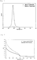
- Figs. 1 and 2 Photoluminescence spectra and UV absorption spectra of the CdS nanocrystals before and after surface treatment are shown in Figs. 1 and 2 , respectively.
- Fig. 1 luminescence peaks are observed at 490nm, and had an FWHM (full width at half maximum) of approximately 25nm.
- the surface treatment did not cause any change in the luminescence wavelengths and a distribution thereof in the nanocrystals, but increased the intensity of the peaks.
- the luminescent efficiency is increased from 10% to 85% after the treatment.
- the surface treatment has little or no influence on the UV absorption, and the two spectra showed ⁇ profiles to each other.
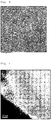
- the HR-TEM confirmed that the CdS nanocrystals have a uniform crystalline structure.
- the TEM image confirmed that the nanocrystals have uniform size distribution and thus arranged in a hexagonal packing structure.
- the precipitates are separated by decanting the solution and dispersing them in 5ml of toluene to obtain a solution of CdTe nanocrystals in toluene. 1ml of the CdTe solution is sampled and about 0.02g of NaBH 4 is added thereto. The resulting mixture is stirred at room temperature for about 10 minutes to reduce the CdTe nanocrystals. Photoluminescence spectra of the CdTe nanocrystals are taken before and after the surface treatment. The photoluminescence spectra confirmed that luminescence peaks are observed at 622nm, and have an FWHM of 60nm. In addition, it is observed that the luminescent efficiency is increased about 5 times after the surface treatment.
- Ethanol as a non-solvent is added to the reaction mixture, and the resulting mixture is then centrifuged. The precipitates are separated by decanting the solution and dispersed in 10ml of toluene to obtain a solution of CdSeS nanocrystals in toluene. 1ml of the CdSeS solution is sampled and about 0.02g of NaBH 4 was added thereto. The resulting mixture is stirred at room temperature for about 30 minutes to reduce the CdSeS nanocrystals. Photoluminescence spectra of the CdSeS nanocrystals are taken before and after the surface treatment. The photoluminescence spectra confirm that luminescence peaks are observed at 552nm, and have an FWHM of approximately 40nm. In addition, it is observed that the luminescent efficiency is increased about 5 times after the surface treatment.
- the precipitates are separated by decanting the solution and dispersed in 10ml of toluene to obtain a solution of CdSe nanocrystals in toluene. 1ml of the CdSe solution is sampled and about 0.02g of NaBH 4 is added thereto. The resulting mixture is stirred at room temperature for about 30 minutes. Photoluminescence spectra of the CdSe nanocrystals are taken before and after the surface treatment. The photoluminescence spectra confirmed that luminescence peaks are observed at 520nm, and have an FWHM of approximately 35nm. In addition, it is observed that the luminescent efficiency is increased about 7 times after the surface treatment.
- Example 5 Fabrication of electroluminescent device using surface-treated CdSe nanocrystals
- PEDOT poly-3,4-ethylenedioxythiophene
- PEDOT poly-3,4-ethylenedioxythiophene
- a solution of 1% by weight of surface-treated CdSe nanocrystals in chlorobenzene is spin-coated and dried to form a luminescent layer having a thickness of 10nm.
- Alq 3 tris(8-hydroxyquinoline) aluminum
- LiF and aluminum are sequentially deposited onto the electron transport layer to thickness of 1 nm and 200nm, respectively, to fabricate an electroluminescent device.
- the luminescence spectrum of the organic electroluminescent device thus fabricated is shown in Fig. 5 . It is observed that luminescence peaks are observed around 520nm, with an FWHM of approximately 40nm. In addition, the brightness of the device is 10 Cd/m 2 and the efficiency of the device is about 0.1%.
Landscapes
- Chemical & Material Sciences (AREA)
- Engineering & Computer Science (AREA)
- Organic Chemistry (AREA)
- Materials Engineering (AREA)
- Crystallography & Structural Chemistry (AREA)
- Nanotechnology (AREA)
- Inorganic Chemistry (AREA)
- Metallurgy (AREA)
- Physics & Mathematics (AREA)
- Life Sciences & Earth Sciences (AREA)
- Biophysics (AREA)
- Optics & Photonics (AREA)
- Composite Materials (AREA)
- Condensed Matter Physics & Semiconductors (AREA)
- General Physics & Mathematics (AREA)
- Manufacturing & Machinery (AREA)
- Luminescent Compositions (AREA)
- Electroluminescent Light Sources (AREA)
Claims (12)
- Verfahren zum Verbessern der Lumineszenzeffizienz eines Halbleiternanokristalls, umfassend folgende Schritte:Reagieren eines Metallvorläufers und eines Chalkogenidvorläufers zum Herstellen eines Halbleiternanokristalls in einem organischen Lösungsmittel bei konstanter Temperatur;Abkühlen des Reaktionsgemischs zum Stoppen des Wachstums des Halbleiternanokristalls;Abtrennen des Halbleiternanokristalls von dem Reaktionsgemisch; undanschließend Inkontaktbringen des abgetrennten Halbleiternanokristalls und eines Reduktionsmittels;wobei das Reduktionsmittel aus Lithiumborhydrid, Lithiumaluminumhydrid, Hydrazin, Schwefelwasserstoff oder Ammoniak ausgewählt ist.
- Verfahren zum Verbessern der Lumineszenzeffizienz eines Kern-Mantel-Halbleiternanokristalls, umfassend folgende Schritte:Herstellen einer Halbleiternanokristallkernzusammensetzung, umfassend einen Halbleiternanokristallkern, der mit einem organischen Dispergiermittel und einem organischen Lösungsmittel koordiniert ist;Zugabe eines Vorläufers zu der Halbleiternanokristallkernzusammensetzung zum Beschichten des Halbleiternanokristallkerns;Abkühlen des Reaktionsgemischs zum Stoppen des Wachstums des Halbleiternanokristallmantels;Abtrennen des Kern-Mantel-Halbleiternanokristalls von dem Reaktionsgemisch; undanschließend Inkontaktbringen des abgetrennten Kern-Mantel-Halbleiternanokristalls und eines Reduktionsmittels;wobei das Reduktionsmittel aus Lithiumborhydrid, Lithiumaluminumhydrid, Hydrazin, Schwefelwasserstoff oder Ammoniak ausgewählt ist.
- Verfahren nach Anspruch 1 oder 2, wobei das Abkühlen durch die Zugabe von mehr Lösungsmittel zu dem Reaktionsgemisch ausgeführt wird.
- Verfahren nach Anspruch 1 oder 2, wobei der Schritt des Regierens eines Metallvorläufers und eines Chalkogenid-Vorläufers zum Herstellen eines Halbleiternanokristalls in einem organischen Lösungsmittel bei einer konstanten Temperatur von 25-350 °C erfolgt.
- Verfahren nach Anspruch 1, wobei der Nanokristall und das Reduktionsmittel in einem Gewichtsverhältnis von 1:10 bis 10:1 gemischt werden.
- Verfahren nach Anspruch 1, wobei das Inkontaktbringen des abgetrennten Kern-Mantel-Halbleiternanokristalls und eines Reduktionsmittels in dem Bereich von 0 bis 100°C ausgeführt wird.
- Verfahren nach Anspruch 2, wobei der Kern-Mantel-Nanokristall und das Reduktionsmittel in einem Gewichtsverhältnis von 1:10 bis 10:1 gemischt werden.
- Verfahren nach Anspruch 2, wobei das Inkontaktbringen des abgetrennten Kern-Mantel-Halbleiternanokristalls und eines Reduktionsmittels in dem Bereich von 0 bis 100 °C ausgeführt wird.
- Verfahren nach Anspruch 1 oder 2, wobei die Halbleiternanokristalle aus mindestens einem Material, ausgewählt aus CdS, CdSe, CdTe, ZnS, ZnSe, ZnTe, HgS, HgSe, HgTe, GaN, GaP, GaAs, InP und InAs hergestellt sind.
- Verfahren nach Anspruch 2, wobei das Dispersionsmittel mindestens eine Verbindung, ausgewählt aus C2-C18-Alkylcarbonsäuren, C2-C18-Alkenylcarbonsäuren, C2-C18-Alkylsulfbnsäuren, C2-C18-Alkenylsulfonsäuren, C2-C18-Phosphonsäuren, C2-C18-Alkylaminen, C2-C18-Alkenylaminen und Salzen davon ist.
- Verfahren nach Anspruch 2, wobei das Dispersionsmittel mindestens eine Verbindung, ausgewählt aus Ölsäure, Stearinsäure, Palmitinsäure, Hexylphosphonsäure, n-Octylphosphonsäure, Tetradecylphosphonsäure, Octadecylphosphonsäure, n-Octylamin und Hexadecylamin ist.
- Verfahren nach Anspruch 1 oder 2, wobei die Nanokristalle eine Form oder eine Mischform aus einer Kugel, einem Stab, einem Tripod, einem Tetrapod, einem Würfel, einem Quader oder einem Stern aufweisen.
Applications Claiming Priority (2)
| Application Number | Priority Date | Filing Date | Title |
|---|---|---|---|
| KR1020030063229A KR100796122B1 (ko) | 2003-09-09 | 2003-09-09 | 화합물 반도체 나노결정의 표면 처리를 통한 양자효율 향상 |
| EP04255157A EP1516944B1 (de) | 2003-09-09 | 2004-08-26 | Erhöhung der Lumineszenzeffizienz von Halbleiter-Nanokristallen durch Oberflächenbehandlung |
Related Parent Applications (2)
| Application Number | Title | Priority Date | Filing Date |
|---|---|---|---|
| EP04255157.2 Division | 2004-08-26 | ||
| EP04255157A Division EP1516944B1 (de) | 2003-09-09 | 2004-08-26 | Erhöhung der Lumineszenzeffizienz von Halbleiter-Nanokristallen durch Oberflächenbehandlung |
Publications (2)
| Publication Number | Publication Date |
|---|---|
| EP2284296A1 EP2284296A1 (de) | 2011-02-16 |
| EP2284296B1 true EP2284296B1 (de) | 2016-05-18 |
Family
ID=34192224
Family Applications (2)
| Application Number | Title | Priority Date | Filing Date |
|---|---|---|---|
| EP10185929.6A Expired - Lifetime EP2284296B1 (de) | 2003-09-09 | 2004-08-26 | Erhöhung der Lumineszenzeffizienz von Halbleiter-Nanokristallen durch Oberflächenbehandlung |
| EP04255157A Expired - Lifetime EP1516944B1 (de) | 2003-09-09 | 2004-08-26 | Erhöhung der Lumineszenzeffizienz von Halbleiter-Nanokristallen durch Oberflächenbehandlung |
Family Applications After (1)
| Application Number | Title | Priority Date | Filing Date |
|---|---|---|---|
| EP04255157A Expired - Lifetime EP1516944B1 (de) | 2003-09-09 | 2004-08-26 | Erhöhung der Lumineszenzeffizienz von Halbleiter-Nanokristallen durch Oberflächenbehandlung |
Country Status (5)
| Country | Link |
|---|---|
| US (1) | US7288468B2 (de) |
| EP (2) | EP2284296B1 (de) |
| JP (1) | JP4928071B2 (de) |
| KR (1) | KR100796122B1 (de) |
| CN (2) | CN101974335B (de) |
Families Citing this family (60)
| Publication number | Priority date | Publication date | Assignee | Title |
|---|---|---|---|---|
| KR100657891B1 (ko) * | 2003-07-19 | 2006-12-14 | 삼성전자주식회사 | 반도체 나노결정 및 그 제조방법 |
| US7553775B2 (en) * | 2004-08-30 | 2009-06-30 | Kabushiki Kaisha Toshiba | Method for coating semiconductor surface, process for production of semiconductor particles using said method, and optical element using said semiconductor particles |
| EP2292718A3 (de) * | 2004-11-11 | 2011-06-22 | Samsung Electronics Co., Ltd | Zusammengewachsene Nanokristalle und Verfahren zu ihrer Herstellung |
| US9637682B2 (en) | 2004-11-11 | 2017-05-02 | Samsung Electronics Co., Ltd. | Interfused nanocrystals and method of preparing the same |
| KR100719574B1 (ko) * | 2005-11-04 | 2007-05-17 | 삼성에스디아이 주식회사 | 평판 디스플레이 장치 및 전자 방출 소자 |
| KR100886084B1 (ko) * | 2005-12-06 | 2009-02-26 | 주식회사 엘지화학 | 코어-쉘 형태의 나노입자 및 그 제조방법 |
| US7517718B2 (en) * | 2006-01-12 | 2009-04-14 | International Business Machines Corporation | Method for fabricating an inorganic nanocomposite |
| EP1978072A4 (de) * | 2006-01-27 | 2009-04-08 | Konica Minolta Med & Graphic | Halbleiternanopartikel mit kern-/hüllenstruktur und herstellungsverfahren dafür |
| KR100754396B1 (ko) * | 2006-02-16 | 2007-08-31 | 삼성전자주식회사 | 양자점 발광소자 및 그 제조방법 |
| KR100678764B1 (ko) * | 2006-02-28 | 2007-02-06 | 한국화학연구원 | 콜로이드상 양자점의 제조방법 |
| WO2007143197A2 (en) * | 2006-06-02 | 2007-12-13 | Qd Vision, Inc. | Light-emitting devices and displays with improved performance |
| KR101057270B1 (ko) * | 2006-03-28 | 2011-08-16 | 샤프 가부시키가이샤 | 13족 질화물 반도체 입자 형광체 및 그의 제조 방법 |
| US11031567B2 (en) * | 2006-07-11 | 2021-06-08 | The Regents Of The University Of Michigan | Efficient solar cells using all-organic nanocrystalline networks |
| WO2008085210A2 (en) * | 2006-09-12 | 2008-07-17 | Qd Vision, Inc. | Electroluminescent display useful for displaying a predetermined pattern |
| WO2008032618A1 (en) * | 2006-09-15 | 2008-03-20 | Konica Minolta Medical & Graphic, Inc. | Semiconductor nanoparticle and process for producing the same |
| KR100759716B1 (ko) * | 2006-09-26 | 2007-10-04 | 고려대학교 산학협력단 | 복합기능 자성체 코어 - 반도체 쉘 나노 입자 및 그의제조방법 |
| KR100759715B1 (ko) * | 2006-09-26 | 2007-10-04 | 고려대학교 산학협력단 | 균일한 크기의 복합기능 나노 입자 제조방법 |
| JP4318710B2 (ja) * | 2006-10-12 | 2009-08-26 | シャープ株式会社 | ナノ結晶粒子蛍光体と被覆ナノ結晶粒子蛍光体、ならびに被覆ナノ結晶粒子蛍光体の製造方法 |
| WO2008133660A2 (en) | 2006-11-21 | 2008-11-06 | Qd Vision, Inc. | Nanocrystals including a group iiia element and a group va element, method, composition, device and other prodcucts |
| WO2008063657A2 (en) * | 2006-11-21 | 2008-05-29 | Qd Vision, Inc. | Light emitting devices and displays with improved performance |
| KR100853086B1 (ko) * | 2007-04-25 | 2008-08-19 | 삼성전자주식회사 | 나노결정-금속산화물 복합체 및 그의 제조방법 |
| WO2008139811A1 (ja) * | 2007-04-26 | 2008-11-20 | Konica Minolta Medical & Graphic, Inc. | 無機ナノ粒子蛍光体の製造方法及び蛍光体標識化合物 |
| US9525148B2 (en) | 2008-04-03 | 2016-12-20 | Qd Vision, Inc. | Device including quantum dots |
| CN102047098B (zh) | 2008-04-03 | 2016-05-04 | Qd视光有限公司 | 包括量子点的发光器件 |
| KR101462652B1 (ko) * | 2008-04-23 | 2014-11-17 | 삼성전자 주식회사 | 양자점-무기 매트릭스 복합체의 제조방법 |
| US11198270B2 (en) | 2008-12-30 | 2021-12-14 | Nanosys, Inc. | Quantum dot films, lighting devices, and lighting methods |
| GB2467162A (en) * | 2009-01-26 | 2010-07-28 | Sharp Kk | Fabrication of nitride nanoparticles |
| GB2467161A (en) * | 2009-01-26 | 2010-07-28 | Sharp Kk | Nitride nanoparticles |
| KR101924080B1 (ko) | 2009-11-11 | 2018-11-30 | 삼성 리서치 아메리카 인코포레이티드 | 양자점을 포함하는 디바이스 |
| WO2011100023A1 (en) | 2010-02-10 | 2011-08-18 | Qd Vision, Inc. | Semiconductor nanocrystals and methods of preparation |
| EP2638321B1 (de) | 2010-11-10 | 2019-05-08 | Nanosys, Inc. | Quantenpunktfilme, beleuchtungsvorrichtungen und beleuchtungsverfahren |
| WO2012099653A2 (en) | 2010-12-08 | 2012-07-26 | Qd Vision, Inc. | Semiconductor nanocrystals and methods of preparation |
| CN103384595B (zh) * | 2010-12-28 | 2016-08-10 | 生命科技公司 | 具有高消光系数的纳米晶体以及这种纳米晶体的制备和使用方法 |
| TWI596188B (zh) * | 2012-07-02 | 2017-08-21 | 奈米系統股份有限公司 | 高度發光奈米結構及其製造方法 |
| CN103122484B (zh) * | 2013-01-10 | 2015-04-15 | 华北电力大学 | 一种调控CsI(Na)晶体发光特性的方法 |
| US10224422B2 (en) * | 2014-12-18 | 2019-03-05 | The Regents Of The University Of California | Method to fabricate quantum dot field-effect transistors without bias-stress effect |
| CN104650856B (zh) * | 2015-02-26 | 2017-01-04 | 江汉大学 | 一种硫化镉量子点溶液的制备方法 |
| EP3296256B1 (de) * | 2015-05-15 | 2021-08-25 | FUJIFILM Corporation | Kern-hülle-partikel und verfahren zur herstellung von kern-hülle-partikeln sowie film |
| TWI737610B (zh) * | 2015-05-20 | 2021-09-01 | 美商納諾光子公司 | 用於改進發光二極體之效率的程序 |
| CN104926155B (zh) * | 2015-05-28 | 2017-09-22 | 福州大学 | 一种金属/有机壳核量子点‑半导体量子点复合发光膜的制备方法 |
| KR20180051606A (ko) * | 2015-09-10 | 2018-05-16 | 메르크 파텐트 게엠베하 | 광-변환 물질 |
| US10829687B2 (en) | 2015-09-15 | 2020-11-10 | 3M Innovative Properties Company | Additive stabilized composite nanoparticles |
| KR20180054676A (ko) | 2015-09-15 | 2018-05-24 | 쓰리엠 이노베이티브 프로퍼티즈 캄파니 | 첨가제 안정화된 복합 나노입자 |
| JP2018533658A (ja) | 2015-10-27 | 2018-11-15 | ルミレッズ リミテッド ライアビリティ カンパニー | 発光装置用の波長変換材料 |
| US10899961B2 (en) | 2016-02-17 | 2021-01-26 | 3M Innovative Properties Company | Quantum dots with stabilizing fluorochemical copolymers |
| US11345849B2 (en) | 2016-07-20 | 2022-05-31 | 3M Innovative Properties Company | Stabilizing styrenic polymer for quantum dots |
| KR20190031505A (ko) | 2016-07-20 | 2019-03-26 | 쓰리엠 이노베이티브 프로퍼티즈 컴파니 | 양자점을 위한 안정화 스티렌계 중합체 |
| JP6756251B2 (ja) * | 2016-11-29 | 2020-09-16 | 東洋インキScホールディングス株式会社 | 量子ドットおよび量子ドット含有組成物 |
| EP3844240B1 (de) * | 2018-05-30 | 2024-02-14 | Shoei Chemical Inc. | Verfahren zur synthese von blau-emittierenden znse1-xtex-legierungsnanokristallen |
| CN110616072A (zh) * | 2018-06-20 | 2019-12-27 | 深圳Tcl工业研究院有限公司 | 一种InP量子点的后处理方法 |
| WO2020073927A1 (zh) * | 2018-10-09 | 2020-04-16 | Tcl集团股份有限公司 | 核壳结构纳米晶的制备方法 |
| WO2020174604A1 (ja) * | 2019-02-27 | 2020-09-03 | シャープ株式会社 | 発光素子およびそれを用いた表示装置 |
| KR102711311B1 (ko) | 2019-04-18 | 2024-09-26 | 삼성전자주식회사 | 리튬 함유 무카드뮴 양자점, 그 제조 방법, 및 이를 포함하는 전자 소자 |
| KR102711312B1 (ko) | 2019-04-18 | 2024-09-26 | 삼성전자주식회사 | 코어쉘 양자점, 그 제조 방법, 및 이를 포함하는 전자 소자 |
| KR102652436B1 (ko) | 2019-04-18 | 2024-03-27 | 삼성전자주식회사 | ZnTeSe 기반의 양자점 |
| CN112397671B (zh) * | 2019-08-19 | 2022-08-23 | Tcl科技集团股份有限公司 | 一种改性硫化锌及其制备方法与量子点发光二极管 |
| CN112397657B (zh) * | 2019-08-19 | 2022-05-03 | Tcl科技集团股份有限公司 | 一种改性硫化锌及其制备方法与量子点发光二极管 |
| CN113046064A (zh) * | 2019-12-28 | 2021-06-29 | Tcl集团股份有限公司 | 量子点材料及其制备方法、量子点发光二极管和发光装置 |
| CN111592877B (zh) * | 2020-03-02 | 2021-05-14 | 河南大学 | 一种核壳结构量子点及其制备方法 |
| CN113060706B (zh) * | 2021-03-23 | 2024-02-09 | 中国科学技术大学 | 一种尺寸可调的胶体ZnSe量子线的制备方法 |
Family Cites Families (12)
| Publication number | Priority date | Publication date | Assignee | Title |
|---|---|---|---|---|
| US6241819B1 (en) * | 1993-04-20 | 2001-06-05 | North American Philips Corp. | Method of manufacturing quantum sized doped semiconductor particles |
| US6322901B1 (en) * | 1997-11-13 | 2001-11-27 | Massachusetts Institute Of Technology | Highly luminescent color-selective nano-crystalline materials |
| JP2004510678A (ja) * | 2000-10-04 | 2004-04-08 | ザ ボード オブ トラスティーズ オブ ザ ユニバーシティ オブ アーカンソー | コロイドナノ結晶の合成 |
| US6576291B2 (en) | 2000-12-08 | 2003-06-10 | Massachusetts Institute Of Technology | Preparation of nanocrystallites |
| CN1169906C (zh) * | 2000-12-14 | 2004-10-06 | 中国科学院长春应用化学研究所 | 有机/无机纳米硫化镉杂化发光材料的合成方法 |
| US6906339B2 (en) * | 2001-09-05 | 2005-06-14 | Rensselaer Polytechnic Institute | Passivated nanoparticles, method of fabrication thereof, and devices incorporating nanoparticles |
| EP1427873A1 (de) * | 2001-09-19 | 2004-06-16 | Evergreen Solar Inc. | Verfahren mit hohe ausbeute zur herstellung von siliciumnanokristallen mit chemisch-zugänglichen oberflächen |
| DE60217530T2 (de) * | 2001-10-02 | 2007-10-18 | Invitrogen Corp., Carlsbad | Verfahren zur halbleiternano partikelsynthese |
| KR100449860B1 (ko) | 2001-12-15 | 2004-09-22 | 에스케이 텔레콤주식회사 | 이동 통신망에서의 심플 인터넷 프로토콜 패킷 망 기반이동 화상전화 서비스 제공 방법 |
| US6878184B1 (en) * | 2002-08-09 | 2005-04-12 | Kovio, Inc. | Nanoparticle synthesis and the formation of inks therefrom |
| CN1174080C (zh) * | 2002-10-10 | 2004-11-03 | 武汉大学 | CdSe/CdS或CdSe/ZnS核/壳型量子点的制备方法 |
| US6853669B2 (en) * | 2002-12-10 | 2005-02-08 | Ut-Battelle, Llc | Nanocrystal waveguide (NOW) laser |
-
2003
- 2003-09-09 KR KR1020030063229A patent/KR100796122B1/ko not_active Expired - Lifetime
-
2004
- 2004-02-25 US US10/785,067 patent/US7288468B2/en not_active Expired - Lifetime
- 2004-08-26 EP EP10185929.6A patent/EP2284296B1/de not_active Expired - Lifetime
- 2004-08-26 EP EP04255157A patent/EP1516944B1/de not_active Expired - Lifetime
- 2004-09-09 CN CN2010102698293A patent/CN101974335B/zh not_active Expired - Lifetime
- 2004-09-09 CN CNA200410078547XA patent/CN1595673A/zh active Pending
- 2004-09-09 JP JP2004262380A patent/JP4928071B2/ja not_active Expired - Lifetime
Also Published As
| Publication number | Publication date |
|---|---|
| US7288468B2 (en) | 2007-10-30 |
| EP2284296A1 (de) | 2011-02-16 |
| JP2005101601A (ja) | 2005-04-14 |
| EP1516944A1 (de) | 2005-03-23 |
| CN101974335A (zh) | 2011-02-16 |
| CN1595673A (zh) | 2005-03-16 |
| US20050051769A1 (en) | 2005-03-10 |
| CN101974335B (zh) | 2013-11-13 |
| JP4928071B2 (ja) | 2012-05-09 |
| EP1516944B1 (de) | 2011-12-21 |
| KR20050026227A (ko) | 2005-03-15 |
| KR100796122B1 (ko) | 2008-01-21 |
Similar Documents
| Publication | Publication Date | Title |
|---|---|---|
| EP2284296B1 (de) | Erhöhung der Lumineszenzeffizienz von Halbleiter-Nanokristallen durch Oberflächenbehandlung | |
| EP1702020B1 (de) | Herstellung von stabilen, hell lumineszierenden nanopartikeln mit zusammensetzungsmässig variierbaren eigenschaften | |
| Talapin et al. | Synthesis and surface modification of amino-stabilized CdSe, CdTe and InP nanocrystals | |
| KR100657891B1 (ko) | 반도체 나노결정 및 그 제조방법 | |
| KR101508568B1 (ko) | 나노입자 | |
| US7138098B2 (en) | Preparation of nanocrystallites | |
| KR101788241B1 (ko) | 분자 클러스터 화합물로부터 금속 산화물 반도체 나노 입자의 합성 | |
| Bhand et al. | Synthesis of CdTe, CdSe and CdTe/CdSe core/shell QDs from wet chemical colloidal method | |
| WO2009094160A2 (en) | Semiconductor nanocrystals | |
| Wang et al. | Preparation and characterization of water-soluble ZnSe: Cu/ZnS core/shell quantum dots | |
| TW201947017A (zh) | 奈米粒子 | |
| KR100745317B1 (ko) | 화합물 반도체 나노결정의 표면 처리를 통한 양자효율 향상 | |
| US11873434B2 (en) | Method for synthesizing a semiconducting nanosized material | |
| Yang et al. | CdSe/Cd1− x Zn x S core/shell quantum dots with tunable emission: growth and morphology evolution | |
| Samokhvalov et al. | Current methods of the synthesis of luminescent semiconductor nanocrystals for biomedical applications | |
| Jung et al. | Optical characteristics of CdSe quantum dots depending on growth conditions and surface passivation | |
| Chung | Foundations of White Light Quantum Dots |
Legal Events
| Date | Code | Title | Description |
|---|---|---|---|
| PUAI | Public reference made under article 153(3) epc to a published international application that has entered the european phase |
Free format text: ORIGINAL CODE: 0009012 |
|
| AC | Divisional application: reference to earlier application |
Ref document number: 1516944 Country of ref document: EP Kind code of ref document: P |
|
| AK | Designated contracting states |
Kind code of ref document: A1 Designated state(s): DE FR GB |
|
| RIN1 | Information on inventor provided before grant (corrected) |
Inventor name: JUN, SHIN AE Inventor name: JANG, EUN JOO Inventor name: SEONG, HYANG SOOK |
|
| 17P | Request for examination filed |
Effective date: 20110816 |
|
| RAP1 | Party data changed (applicant data changed or rights of an application transferred) |
Owner name: SAMSUNG ELECTRONICS CO., LTD. |
|
| GRAP | Despatch of communication of intention to grant a patent |
Free format text: ORIGINAL CODE: EPIDOSNIGR1 |
|
| RIC1 | Information provided on ipc code assigned before grant |
Ipc: C30B 7/00 20060101AFI20151203BHEP Ipc: C09K 11/88 20060101ALI20151203BHEP Ipc: H01L 33/00 20100101ALI20151203BHEP Ipc: B82Y 20/00 20110101ALI20151203BHEP Ipc: C09C 1/38 20060101ALI20151203BHEP Ipc: H05B 33/14 20060101ALI20151203BHEP Ipc: B82Y 30/00 20110101ALI20151203BHEP Ipc: C30B 33/00 20060101ALI20151203BHEP Ipc: C01B 19/00 20060101ALI20151203BHEP Ipc: C09C 1/10 20060101ALI20151203BHEP Ipc: H01L 51/50 20060101ALI20151203BHEP Ipc: C09C 1/12 20060101ALI20151203BHEP Ipc: C09K 11/56 20060101ALI20151203BHEP |
|
| INTG | Intention to grant announced |
Effective date: 20151223 |
|
| GRAS | Grant fee paid |
Free format text: ORIGINAL CODE: EPIDOSNIGR3 |
|
| GRAA | (expected) grant |
Free format text: ORIGINAL CODE: 0009210 |
|
| AC | Divisional application: reference to earlier application |
Ref document number: 1516944 Country of ref document: EP Kind code of ref document: P |
|
| AK | Designated contracting states |
Kind code of ref document: B1 Designated state(s): DE FR GB |
|
| REG | Reference to a national code |
Ref country code: GB Ref legal event code: FG4D |
|
| REG | Reference to a national code |
Ref country code: DE Ref legal event code: R096 Ref document number: 602004049346 Country of ref document: DE |
|
| REG | Reference to a national code |
Ref country code: FR Ref legal event code: PLFP Year of fee payment: 13 |
|
| REG | Reference to a national code |
Ref country code: DE Ref legal event code: R097 Ref document number: 602004049346 Country of ref document: DE |
|
| PLBE | No opposition filed within time limit |
Free format text: ORIGINAL CODE: 0009261 |
|
| STAA | Information on the status of an ep patent application or granted ep patent |
Free format text: STATUS: NO OPPOSITION FILED WITHIN TIME LIMIT |
|
| 26N | No opposition filed |
Effective date: 20170221 |
|
| REG | Reference to a national code |
Ref country code: FR Ref legal event code: PLFP Year of fee payment: 14 |
|
| REG | Reference to a national code |
Ref country code: FR Ref legal event code: PLFP Year of fee payment: 15 |
|
| P01 | Opt-out of the competence of the unified patent court (upc) registered |
Effective date: 20230530 |
|
| PGFP | Annual fee paid to national office [announced via postgrant information from national office to epo] |
Ref country code: GB Payment date: 20230720 Year of fee payment: 20 |
|
| PGFP | Annual fee paid to national office [announced via postgrant information from national office to epo] |
Ref country code: FR Payment date: 20230725 Year of fee payment: 20 Ref country code: DE Payment date: 20230720 Year of fee payment: 20 |
|
| REG | Reference to a national code |
Ref country code: DE Ref legal event code: R071 Ref document number: 602004049346 Country of ref document: DE |
|
| REG | Reference to a national code |
Ref country code: GB Ref legal event code: PE20 Expiry date: 20240825 |
|
| PG25 | Lapsed in a contracting state [announced via postgrant information from national office to epo] |
Ref country code: GB Free format text: LAPSE BECAUSE OF EXPIRATION OF PROTECTION Effective date: 20240825 |
|
| PG25 | Lapsed in a contracting state [announced via postgrant information from national office to epo] |
Ref country code: GB Free format text: LAPSE BECAUSE OF EXPIRATION OF PROTECTION Effective date: 20240825 |