EP2268568B1 - Method of sealing a cavity - Google Patents
Method of sealing a cavity Download PDFInfo
- Publication number
- EP2268568B1 EP2268568B1 EP09712954.8A EP09712954A EP2268568B1 EP 2268568 B1 EP2268568 B1 EP 2268568B1 EP 09712954 A EP09712954 A EP 09712954A EP 2268568 B1 EP2268568 B1 EP 2268568B1
- Authority
- EP
- European Patent Office
- Prior art keywords
- passage
- layer
- cavity
- substrate
- sacrificial
- Prior art date
- Legal status (The legal status is an assumption and is not a legal conclusion. Google has not performed a legal analysis and makes no representation as to the accuracy of the status listed.)
- Active
Links
Images


Classifications
-
- B—PERFORMING OPERATIONS; TRANSPORTING
- B81—MICROSTRUCTURAL TECHNOLOGY
- B81C—PROCESSES OR APPARATUS SPECIALLY ADAPTED FOR THE MANUFACTURE OR TREATMENT OF MICROSTRUCTURAL DEVICES OR SYSTEMS
- B81C1/00—Manufacture or treatment of devices or systems in or on a substrate
- B81C1/00015—Manufacture or treatment of devices or systems in or on a substrate for manufacturing microsystems
- B81C1/00261—Processes for packaging MEMS devices
- B81C1/00277—Processes for packaging MEMS devices for maintaining a controlled atmosphere inside of the cavity containing the MEMS
- B81C1/00293—Processes for packaging MEMS devices for maintaining a controlled atmosphere inside of the cavity containing the MEMS maintaining a controlled atmosphere with processes not provided for in B81C1/00285
-
- B—PERFORMING OPERATIONS; TRANSPORTING
- B81—MICROSTRUCTURAL TECHNOLOGY
- B81C—PROCESSES OR APPARATUS SPECIALLY ADAPTED FOR THE MANUFACTURE OR TREATMENT OF MICROSTRUCTURAL DEVICES OR SYSTEMS
- B81C2203/00—Forming microstructural systems
- B81C2203/01—Packaging MEMS
- B81C2203/0145—Hermetically sealing an opening in the lid
Definitions
- Embodiments of the present invention generally relate to a method of sealing a cavity in a micro-electromechanical system (MEMS) or a nano-electromechanical system (NEMS).
- MEMS micro-electromechanical system
- NEMS nano-electromechanical system
- MEMS and NEMS devices require encapsulation in a low or very low pressure environment. This is especially true for transducers, such as those used in inertial sensors, which are affected by squeeze-film damping effects.
- methods such as Chemical Vapor Deposition (CVD) have been used to the seal cavities in which MEMS devices are enclosed.
- CVD Chemical Vapor Deposition
- Embodiments disclosed herein generally include methods of sealing a cavity in a device structure.
- the cavity may be opened by etching away sacrificial material that may define the cavity volume. Material from below the cavity, above the cavity, and outside the cavity may be sputter etched and redeposited over and in passageways leading to the cavity to thereby seal the cavity. Material may be sputter etched from above the cavity and redeposited in the passageways leading to the cavity as well.
- the sputter etching may occur in a substantially inert atmosphere. As the sputter etching is a physical process, little or no sputter etched material will redeposit within the cavity itself.
- the inert gases may sweep out any residual gases that may be present in the cavity after the cavity has been opened. Thus, after the sputter etching, the cavity may be substantially filled with inert gases that do not negatively impact the cavity.
- the invention further comprises:
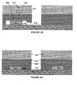
- FIG. 1 is a schematic top view of a structure 100 having a plurality of cavities according to one embodiment.
- the structure 100 comprises a substrate 102 having one or more layers 104 formed thereover. Between the layers 104 and the substrate 102, one or more cavities may be formed.
- one or more sacrificial layers of sacrificial material 108 may be formed between the substrate 102 and the one or more layers 104.
- the sacrificial material 108 may define the volume of open space within the cavity to be formed.
- the cavity is formed by removing the sacrificial material 108.
- one or more devices 106 may be present.
- Sacrificial material 108 may be present in a passage 110 through the cavity area.
- the passage 110 may permit etching gases or liquids enter into the cavity and remove the sacrificial material 108.
- sacrificial material 108 may also be exposed over the substrate 102 as a channel 112 between the one or more layers 104.
- the devices 106 Upon removal of the sacrificial material 108, the devices 106 will be released within the cavities. It is to be understood that while the passages 110 have been shown on one side of the eventual cavity, the passages 110 may be on both sides of the cavity to be formed. Additionally, while the passages 110 have been shown as straight with a line of sight to the devices 106, the passages 110 may be shaped to provide little or no line of sight to the devices 106.
- Figure 2 is a schematic top view of a structure 200 having a cavity 204 according to another embodiment.
- the cavity 204 is formed over a substrate 202 and is accessed through one or more passages 208.
- the passages 208 have a kink such that there is no line of sight path between the device 206 contained in the cavity 204 and the entrance to the passages 208. It is to be understood that while the passages 208 have been shown on one side of the cavity 204, the passages 208 may be present on both sides. Additionally, while the passages 208 have been shown as blocking any line of sight path to the device 206, the passages 208 may be designed to provide a complete or less than complete line of sight path to the device 206.
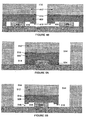
- Figure 3A is a schematic side view of a structure having a side release passage having a height less than a height of the cavity.
- Figure 3B is a schematic side view of the structure of Figure 3A having the sacrificial material removed.
- the structure has a substrate 302 upon which a device 306 may be formed.
- the substrate 302 may comprise a silicon based material.
- the substrate 302 may comprise multiple layers of a device structure such as a CMOS structure.
- the device 306 may comprise any MEMS, NEMS, micro-opto-electromechanical system (MOEMS) device, nano-opto-electromechanical system (NOEMS) device, or combinations thereof.
- the device may be formed at any point within the structure.
- the device may be formed above or below a CMOS structure. Additionally, the device may be formed within a stack such that additional layers of the structure ( i.e., not the device) may be present above the device.
- the device may be used in the back end of line (BEOL) processing of a metal system.
- BEOL back end of line
- the device may also be formed in the back end of line of any other semiconductor front end technology, such as a bipolar process, or a bi-CMOS, or a SiGe, or a GaAs, GaAlAs or other III/V or II/VI, or any other front end semiconductor process.
- the device may be formed on glass. It is to be understood that while one device 306 is shown, multiple devices 306 may be present. If multiple devices 306 are present, the devices 306 may be identical or different and may perform the same or different functions. Also, while a device 306 has been shown, it is to be understood that the device 306 may not be present.
- the device 306 may be enclosed in a sacrificial material 304.
- the sacrificial material 304 may comprise a spin-on organic film.
- PECVD Plasma Enhanced Chemical Vapor Deposition
- Additional deposition methods that may be used to deposit the sacrificial material 304 include atomic layer deposition (ALD), physical vapor deposition (PVD), chemical vapor deposition (CVD), and other conventional deposition methods.
- a spin on sacrificial material 304 may flow over any irregularities in the underlying layers, thereby producing a flat layer where the thickness of the film depends on the height of the underlying material.
- the sacrificial material 304 may be deposited and then patterned to remove portions of the sacrificial material 304 that do not affect the cavity to be formed.
- the trench may extend for a distance along the Z axis for about 1 mm or greater.
- the ratio of the height to the width is known as an aspect ratio.
- the aspect ratio opening may be proportional to an ejection cosine distribution of sputtered material.
- the aspect ratio may be proportional to the angular distribution of the incoming species. By proportional, it is to be understood to include not only linearly proportional, but also inversely proportional, and any general relationship between the aspect ratio and the sputtered material.
- the aspect ratio of the trench 314 may be about 1:1. In another embodiment, the aspect ratio of the trench 314 may be greater than about 2:1.
- the width may be between about several nanometers to about a hundred micrometers. In one embodiment, the width may be between about 1 micrometer to about 50 micrometers.
- the sacrificial material 304 after patterning, provides the shape of the cavity 316 to be formed as well as the release passage 318.
- the cavity 316 may have a height shown by arrows "C” while the passage 318 may have a height shown by arrows "D".
- the passage 318 may extend along the trench for the entire length of the trench along the Z axis. In one embodiment, the passage 318 may extend along the trench for less than the entire length along the Z axis. In the embodiment shown in Figures 3A and 3B , the passage 318 has a height less than a height of the cavity 316. It is to be understood that the passage 318 may have a height substantially equal to the height of the cavity 316 if desired. In one embodiment, the cavity release passage 318 may have a height of about 10 micrometers or less.
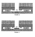
- the devices 406 may be enclosed in a sacrificial material 404.
- the sacrificial material 404 may comprise a spin-on organic film.
- spin-on films PECVD, ALD, CVD, or PVD materials, such as silicon nitride, silicon dioxide, amorphous silicon and amorphous carbon, can be employed to the same effect.
- a spin on sacrificial material 404 may flow over any irregularities in the underlying layers, thereby producing a flat layer where the thickness of the film depends on the height of the underlying material.
- the sacrificial material 404 may be deposited and then patterned to remove portions of the sacrificial material 404 that do not affect the cavity to be formed.
- the sacrificial material 404 may be patterned such that the sacrificial material 404 spans the trench 414 so that the etching gases or liquid that removes the remainder of the sacrificial material 404 may encounter the sacrificial material 404 from the top rather than from the side through the passage 418.
- One or more other layers 408, 410, and 412 may be deposited over the sacrificial material 404.
- the one or more other layers 408, 410, and 412 may form a part of a structure to be formed above the device 406.
- a trench 414 may be formed in the structure by patterning the one or more other layers 408, 410, and 412. The patterning may comprise etching.
- Figure 5A is a schematic side view of a structure having a plurality of side release passages having a height less than a height of the cavity.
- Figure 5B is a schematic side view of the structure of Figure 5A having the sacrificial material removed.
- the structure has a substrate 502 upon which one or more devices 506 may be formed.
- the substrate 502 may comprise a silicon based material.
- the substrate 502 may comprise multiple layers of a device structure such as a CMOS structure.
- the devices 506 may comprise any MEMS, NEMS, MOEMS, or NOEMS device, or combinations thereof.
- the devices 506 that may comprise a microfluidic channel that provides temperature control and improved reliability in integrated circuits.
- the devices 506, in general can be any device that may be sealed within a cavity over a substrate.
- One or more other layers 508, 510, and 512 may be deposited over the sacrificial material 504.
- the one or more other layers 508, 510, and 512 may form a part of a structure to be formed above the device 506.
- a trench 514 may be formed in the structure by patterning the one or more other layers 508, 510, and 512.
- the passages to the cavities may need to be closed.
- CVD processes may not be appropriate as these will lead to the deposition of material on the active area of the device. This problem arises because plasma activated species (e.g., Si-based, metal-based or Oxygen-based species) will have a lifetime which will be long enough to reach the active area inside the cavity and may therefore be deposited on a device or other surface inside the cavity.
- plasma activated species e.g., Si-based, metal-based or Oxygen-based species
- the gas medium surrounding the device should also be as noble as possible to avoid any reaction that could adversely affect the device or its lifetime operation. This is especially true for transducers that may heat up during their operation and reach a level at which they react with residual gases trapped into the cavity. Therefore, chemical based processes may not be appropriate as they involve reactive gases.
- the encapsulation or sealing of the cavity has to be performed without deposition of materials on the active device as this would jeopardize the device operations.
- methods of physical sputtering may be used. These methods typically involve the physical vaporization of atoms from a surface by bombarding that surface with energetic atomized particles, thereby transferring the momentum of the particles to the atoms of the surface.
- the energetic particles usually Argon (Ar) or Helium (He)
- Argon Argon
- He Helium
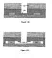
- the plasma is located away from the substrate 902.
- the gases used for sputter etching should not be accelerated toward the external target but toward the substrate 902. This can be performed on an apparatus where the substrate 902 can be negatively biased, for example when a RF bias is applied to it, with respect to the plasma.
- the horizontal and vertical design of the layers of the structure may be implemented such that they do not have any direct line-of-sight path between the enclosed device and the release hole entrance.
- the pressure in the apparatus could be as low as a few mT and as high as the maximum pressure which could be handled by the chamber. A higher pressure would maximize the amount of sidewall redeposition and is hence favorable for the sealing. However, the upper pressure can also be defined by the device requirements.
Landscapes
- Engineering & Computer Science (AREA)
- Microelectronics & Electronic Packaging (AREA)
- Manufacturing & Machinery (AREA)
- Micromachines (AREA)
- Drying Of Semiconductors (AREA)
- Physical Vapour Deposition (AREA)
Applications Claiming Priority (3)
| Application Number | Priority Date | Filing Date | Title |
|---|---|---|---|
| US6665508P | 2008-02-22 | 2008-02-22 | |
| US12/267,186 US7989262B2 (en) | 2008-02-22 | 2008-11-07 | Method of sealing a cavity |
| PCT/US2009/033927 WO2009105382A2 (en) | 2008-02-22 | 2009-02-12 | Method of sealing a cavity |
Publications (2)
| Publication Number | Publication Date |
|---|---|
| EP2268568A2 EP2268568A2 (en) | 2011-01-05 |
| EP2268568B1 true EP2268568B1 (en) | 2014-12-17 |
Family
ID=40986138
Family Applications (1)
| Application Number | Title | Priority Date | Filing Date |
|---|---|---|---|
| EP09712954.8A Active EP2268568B1 (en) | 2008-02-22 | 2009-02-12 | Method of sealing a cavity |
Country Status (6)
| Country | Link |
|---|---|
| US (2) | US7989262B2 (enExample) |
| EP (1) | EP2268568B1 (enExample) |
| JP (2) | JP2011513073A (enExample) |
| CN (1) | CN101998930B (enExample) |
| TW (1) | TWI353338B (enExample) |
| WO (1) | WO2009105382A2 (enExample) |
Families Citing this family (10)
| Publication number | Priority date | Publication date | Assignee | Title |
|---|---|---|---|---|
| US20120244715A1 (en) * | 2009-12-02 | 2012-09-27 | Xactix, Inc. | High-selectivity etching system and method |
| EP2699512B1 (en) * | 2011-04-20 | 2016-05-25 | Cavendish Kinetics Inc. | Implantation of gaseous chemicals into cavities formed in intermediate dielectric layers for subsequent thermal diffusion release |
| US8492187B2 (en) | 2011-09-29 | 2013-07-23 | International Business Machines Corporation | High throughput epitaxial liftoff for releasing multiple semiconductor device layers from a single base substrate |
| SE537584C2 (sv) | 2011-12-15 | 2015-06-30 | Silex Microsystems Ab | Tunnfilmskapsling |
| KR20160024361A (ko) | 2013-06-27 | 2016-03-04 | 소이텍 | 희생 재료로 충전된 공동을 포함하는 반도체 구조를 제조하는 방법들 |
| US9330929B1 (en) * | 2014-10-13 | 2016-05-03 | Infineon Technologies Dresden Gmbh | Systems and methods for horizontal integration of acceleration sensor structures |
| CN105977221B (zh) * | 2016-04-28 | 2018-11-06 | 清华大学 | 气密性封装结构及封装方法 |
| WO2018017134A1 (en) * | 2016-07-22 | 2018-01-25 | Hewlett-Packard Development Company, L.P. | Substrate assembly and related methods |
| DE102017218635B4 (de) * | 2017-10-18 | 2021-03-18 | Infineon Technologies Ag | Verfahren zum Verschließen einer Zugangsöffnung zu einer Kavität und MEMS-Bauelement mit einem Verschlusselement |
| DE102019120886A1 (de) * | 2019-08-02 | 2021-02-04 | Infineon Technologies Ag | Halbleitergehäuse mit einem Hohlraum in seinem Gehäusekörper |
Citations (1)
| Publication number | Priority date | Publication date | Assignee | Title |
|---|---|---|---|---|
| JP2007253265A (ja) * | 2006-03-22 | 2007-10-04 | Sony Corp | 電気機械素子の製造方法 |
Family Cites Families (87)
| Publication number | Priority date | Publication date | Assignee | Title |
|---|---|---|---|---|
| JPS63183181A (ja) * | 1987-01-23 | 1988-07-28 | Anelva Corp | マグネトロンスパツタエツチング装置 |
| JPS63198378A (ja) | 1987-02-13 | 1988-08-17 | Nissan Motor Co Ltd | 振動センサの製造方法 |
| JPS63307758A (ja) | 1987-06-09 | 1988-12-15 | Nec Corp | 集積回路装置 |
| US5279669A (en) * | 1991-12-13 | 1994-01-18 | International Business Machines Corporation | Plasma reactor for processing substrates comprising means for inducing electron cyclotron resonance (ECR) and ion cyclotron resonance (ICR) conditions |
| JP3287038B2 (ja) | 1991-12-19 | 2002-05-27 | ソニー株式会社 | 液晶表示装置 |
| US5270264A (en) * | 1991-12-20 | 1993-12-14 | Intel Corporation | Process for filling submicron spaces with dielectric |
| US5292370A (en) * | 1992-08-14 | 1994-03-08 | Martin Marietta Energy Systems, Inc. | Coupled microwave ECR and radio-frequency plasma source for plasma processing |
| US5346578A (en) * | 1992-11-04 | 1994-09-13 | Novellus Systems, Inc. | Induction plasma source |
| US5614055A (en) * | 1993-08-27 | 1997-03-25 | Applied Materials, Inc. | High density plasma CVD and etching reactor |
| US5504026A (en) * | 1995-04-14 | 1996-04-02 | Analog Devices, Inc. | Methods for planarization and encapsulation of micromechanical devices in semiconductor processes |
| US5578976A (en) | 1995-06-22 | 1996-11-26 | Rockwell International Corporation | Micro electromechanical RF switch |
| US5696662A (en) | 1995-08-21 | 1997-12-09 | Honeywell Inc. | Electrostatically operated micromechanical capacitor |
| US6012336A (en) * | 1995-09-06 | 2000-01-11 | Sandia Corporation | Capacitance pressure sensor |
| DE19638666C1 (de) | 1996-01-08 | 1997-11-20 | Siemens Ag | Schmelzsicherung mit einer Schutzschicht in einer integrierten Halbleiterschaltung sowie zugehöriges Herstellungsverfahren |
| US5807467A (en) * | 1996-01-22 | 1998-09-15 | Micron Technology, Inc. | In situ preclean in a PVD chamber with a biased substrate configuration |
| US5730835A (en) * | 1996-01-31 | 1998-03-24 | Micron Technology, Inc. | Facet etch for improved step coverage of integrated circuit contacts |
| JPH09257618A (ja) | 1996-03-26 | 1997-10-03 | Toyota Central Res & Dev Lab Inc | 静電容量型圧力センサおよびその製造方法 |
| US5919548A (en) * | 1996-10-11 | 1999-07-06 | Sandia Corporation | Chemical-mechanical polishing of recessed microelectromechanical devices |
| US6268661B1 (en) * | 1999-08-31 | 2001-07-31 | Nec Corporation | Semiconductor device and method of its fabrication |
| US5980349A (en) * | 1997-05-14 | 1999-11-09 | Micron Technology, Inc. | Anodically-bonded elements for flat panel displays |
| US5872058A (en) * | 1997-06-17 | 1999-02-16 | Novellus Systems, Inc. | High aspect ratio gapfill process by using HDP |
| DE19742729A1 (de) * | 1997-09-26 | 1999-04-01 | Sca Hygiene Prod Gmbh | Verfahren zur Aufbereitung von Altpapier unter Vermeidung von Bioziden und Chlorverbindungen, sowie von Wasserstoffperoxid und Peressigsäure, Einrichtung zur Ausführung dieses Verfahrens sowie Recycling Tissuepapiere mit einer Gesamtkeimzahl kleiner 1000 KBE/g und einer Oberflächenkeimzahl kleiner 20 KBE/dm·2· |
| JPH11177067A (ja) | 1997-12-09 | 1999-07-02 | Sony Corp | メモリ素子およびメモリアレイ |
| US6395150B1 (en) * | 1998-04-01 | 2002-05-28 | Novellus Systems, Inc. | Very high aspect ratio gapfill using HDP |
| FR2781499B1 (fr) * | 1998-07-24 | 2000-09-08 | Atochem Elf Sa | Compositions de nettoyage ou de sechage a base de 1,1,1,2,3,4,4,5,5, 5 - decafluoropentane |
| US6153839A (en) | 1998-10-22 | 2000-11-28 | Northeastern University | Micromechanical switching devices |
| CN1276259C (zh) | 1998-12-02 | 2006-09-20 | 佛姆法克特股份有限公司 | 光刻接触元件 |
| JP2000186931A (ja) | 1998-12-21 | 2000-07-04 | Murata Mfg Co Ltd | 小型電子部品及びその製造方法並びに該小型電子部品に用いるビアホールの成形方法 |
| US6174820B1 (en) * | 1999-02-16 | 2001-01-16 | Sandia Corporation | Use of silicon oxynitride as a sacrificial material for microelectromechanical devices |
| US6274440B1 (en) | 1999-03-31 | 2001-08-14 | International Business Machines Corporation | Manufacturing of cavity fuses on gate conductor level |
| US6633055B2 (en) * | 1999-04-30 | 2003-10-14 | International Business Machines Corporation | Electronic fuse structure and method of manufacturing |
| US6287940B1 (en) | 1999-08-02 | 2001-09-11 | Honeywell International Inc. | Dual wafer attachment process |
| US6500694B1 (en) * | 2000-03-22 | 2002-12-31 | Ziptronix, Inc. | Three dimensional device integration method and integrated device |
| US6310339B1 (en) | 1999-10-28 | 2001-10-30 | Hrl Laboratories, Llc | Optically controlled MEM switches |
| JP2001133703A (ja) | 1999-11-04 | 2001-05-18 | Seiko Epson Corp | 半導体基板上に構造物を有する装置の製造方法および装置 |
| US20010040675A1 (en) | 2000-01-28 | 2001-11-15 | True Randall J. | Method for forming a micromechanical device |
| US6439693B1 (en) | 2000-05-04 | 2002-08-27 | Silverbrook Research Pty Ltd. | Thermal bend actuator |
| DE10024266B4 (de) * | 2000-05-17 | 2010-06-17 | Robert Bosch Gmbh | Verfahren zur Herstellung eines mikromechanischen Bauelements |
| US7153717B2 (en) * | 2000-05-30 | 2006-12-26 | Ic Mechanics Inc. | Encapsulation of MEMS devices using pillar-supported caps |
| US7008812B1 (en) * | 2000-05-30 | 2006-03-07 | Ic Mechanics, Inc. | Manufacture of MEMS structures in sealed cavity using dry-release MEMS device encapsulation |
| WO2002016150A1 (en) | 2000-08-23 | 2002-02-28 | Reflectivity, Inc. | Transition metal dielectric alloy materials for mems |
| US6535091B2 (en) | 2000-11-07 | 2003-03-18 | Sarnoff Corporation | Microelectronic mechanical systems (MEMS) switch and method of fabrication |
| DE10056716B4 (de) | 2000-11-15 | 2007-10-18 | Robert Bosch Gmbh | Mikrostrukturbauelement |
| DE10104868A1 (de) * | 2001-02-03 | 2002-08-22 | Bosch Gmbh Robert | Mikromechanisches Bauelement sowie ein Verfahren zur Herstellung eines mikromechanischen Bauelements |
| JP2002280470A (ja) | 2001-03-22 | 2002-09-27 | Aisin Seiki Co Ltd | 半導体装置及びその製造方法 |
| US6958123B2 (en) * | 2001-06-15 | 2005-10-25 | Reflectivity, Inc | Method for removing a sacrificial material with a compressed fluid |
| JP2003035874A (ja) | 2001-07-23 | 2003-02-07 | Nikon Corp | 薄膜スライド接続機構及びその製造方法並びにこれを用いたミラーデバイス及び光スイッチ |
| US6930364B2 (en) * | 2001-09-13 | 2005-08-16 | Silicon Light Machines Corporation | Microelectronic mechanical system and methods |
| WO2003028059A1 (en) | 2001-09-21 | 2003-04-03 | Hrl Laboratories, Llc | Mems switches and methods of making same |
| US6635506B2 (en) * | 2001-11-07 | 2003-10-21 | International Business Machines Corporation | Method of fabricating micro-electromechanical switches on CMOS compatible substrates |
| ATE417021T1 (de) * | 2001-11-09 | 2008-12-15 | Wispry Inc | Mems-einrichtung mit dreischichtigem strahl und diesbezügliche verfahren |
| FR2835963B1 (fr) | 2002-02-11 | 2006-03-10 | Memscap | Micro-composant du type micro-interrupteur et procede de fabrication d'un tel micro-composant |
| US6946382B2 (en) | 2002-04-02 | 2005-09-20 | Dow Global Technologies Inc. | Process for making air gap containing semiconducting devices and resulting semiconducting device |
| US6635509B1 (en) * | 2002-04-12 | 2003-10-21 | Dalsa Semiconductor Inc. | Wafer-level MEMS packaging |
| AU2003228973A1 (en) * | 2002-05-07 | 2003-11-11 | Memgen Corporation | Electrochemically fabricated hermetically sealed microstructures |
| US7064637B2 (en) * | 2002-07-18 | 2006-06-20 | Wispry, Inc. | Recessed electrode for electrostatically actuated structures |
| US7429495B2 (en) * | 2002-08-07 | 2008-09-30 | Chang-Feng Wan | System and method of fabricating micro cavities |
| AU2003286572A1 (en) * | 2002-10-23 | 2004-05-13 | Rutgers, The State University Of New Jersey | Processes for hermetically packaging wafer level microscopic structures |
| TWI236453B (en) | 2002-12-03 | 2005-07-21 | Microfabrica Inc | Electrochemical fabrication process for producing a three-dimensional structure from a plurality of adhered layers |
| EP1433740A1 (en) | 2002-12-24 | 2004-06-30 | Interuniversitair Microelektronica Centrum Vzw | Method for the closure of openings in a film |
| US20040157426A1 (en) * | 2003-02-07 | 2004-08-12 | Luc Ouellet | Fabrication of advanced silicon-based MEMS devices |
| EP1450406A1 (en) | 2003-02-19 | 2004-08-25 | Cavendish Kinetics Limited | Micro fuse |
| US20040166603A1 (en) * | 2003-02-25 | 2004-08-26 | Carley L. Richard | Micromachined assembly with a multi-layer cap defining a cavity |
| NL1023275C2 (nl) | 2003-04-25 | 2004-10-27 | Cavendish Kinetics Ltd | Werkwijze voor het vervaardigen van een micro-mechanisch element. |
| WO2004101855A2 (en) | 2003-05-07 | 2004-11-25 | Microfabrica Inc. | Electrochemical fabrication methods including use of surface treatments to reduce overplating and/or planarization during formation of multi-layer three-dimensional structures |
| US6917459B2 (en) * | 2003-06-03 | 2005-07-12 | Hewlett-Packard Development Company, L.P. | MEMS device and method of forming MEMS device |
| WO2005015637A1 (ja) * | 2003-08-08 | 2005-02-17 | Matsushita Electric Industrial Co., Ltd. | 電子デバイスおよびその製造方法 |
| US7060624B2 (en) * | 2003-08-13 | 2006-06-13 | International Business Machines Corporation | Deep filled vias |
| US6861277B1 (en) * | 2003-10-02 | 2005-03-01 | Hewlett-Packard Development Company, L.P. | Method of forming MEMS device |
| DE10353767B4 (de) | 2003-11-17 | 2005-09-29 | Infineon Technologies Ag | Vorrichtung zur Häusung einer mikromechanischen Struktur und Verfahren zur Herstellung derselben |
| US7163896B1 (en) * | 2003-12-10 | 2007-01-16 | Novellus Systems, Inc. | Biased H2 etch process in deposition-etch-deposition gap fill |
| US7344996B1 (en) * | 2005-06-22 | 2008-03-18 | Novellus Systems, Inc. | Helium-based etch process in deposition-etch-deposition gap fill |
| JP2005183557A (ja) | 2003-12-18 | 2005-07-07 | Canon Inc | 半導体集積回路とその動作方法、該回路を備えたicカード |
| FR2864340B1 (fr) * | 2003-12-19 | 2006-03-24 | Commissariat Energie Atomique | Microcomposant comportant une microcavite hermetique et procede de fabrication d'un tel microcomposant |
| GB0330010D0 (en) | 2003-12-24 | 2004-01-28 | Cavendish Kinetics Ltd | Method for containing a device and a corresponding device |
| JP4617743B2 (ja) * | 2004-07-06 | 2011-01-26 | ソニー株式会社 | 機能素子およびその製造方法、ならびに流体吐出ヘッド |
| FR2874213B1 (fr) * | 2004-08-13 | 2007-03-02 | Commissariat Energie Atomique | Dispositif comprenant un microsysteme encapsule et procede de fabrication |
| US7344907B2 (en) * | 2004-11-19 | 2008-03-18 | International Business Machines Corporation | Apparatus and methods for encapsulating microelectromechanical (MEM) devices on a wafer scale |
| US7482193B2 (en) * | 2004-12-20 | 2009-01-27 | Honeywell International Inc. | Injection-molded package for MEMS inertial sensor |
| US7211525B1 (en) * | 2005-03-16 | 2007-05-01 | Novellus Systems, Inc. | Hydrogen treatment enhanced gap fill |
| US7576426B2 (en) * | 2005-04-01 | 2009-08-18 | Skyworks Solutions, Inc. | Wafer level package including a device wafer integrated with a passive component |
| US7329586B2 (en) * | 2005-06-24 | 2008-02-12 | Applied Materials, Inc. | Gapfill using deposition-etch sequence |
| GB0515980D0 (en) | 2005-08-03 | 2005-09-07 | Cavendish Kinetics Ltd | Memory cell for a circuit and method of operation therefor |
| GB0516148D0 (en) | 2005-08-05 | 2005-09-14 | Cavendish Kinetics Ltd | Method of integrating an element |
| GB0523713D0 (en) | 2005-11-22 | 2005-12-28 | Cavendish Kinetics Ltd | Enclosure method |
| GB0523715D0 (en) | 2005-11-22 | 2005-12-28 | Cavendish Kinetics Ltd | Method of minimising contact area |
| US20070235501A1 (en) * | 2006-03-29 | 2007-10-11 | John Heck | Self-packaging MEMS device |
-
2008
- 2008-11-07 US US12/267,186 patent/US7989262B2/en active Active
-
2009
- 2009-02-12 CN CN200980112054.4A patent/CN101998930B/zh active Active
- 2009-02-12 WO PCT/US2009/033927 patent/WO2009105382A2/en not_active Ceased
- 2009-02-12 JP JP2010547696A patent/JP2011513073A/ja active Pending
- 2009-02-12 EP EP09712954.8A patent/EP2268568B1/en active Active
- 2009-02-19 TW TW098105313A patent/TWI353338B/zh active
-
2011
- 2011-08-01 US US13/195,215 patent/US8395249B2/en active Active
-
2012
- 2012-09-12 JP JP2012200158A patent/JP2013031919A/ja active Pending
Patent Citations (1)
| Publication number | Priority date | Publication date | Assignee | Title |
|---|---|---|---|---|
| JP2007253265A (ja) * | 2006-03-22 | 2007-10-04 | Sony Corp | 電気機械素子の製造方法 |
Also Published As
| Publication number | Publication date |
|---|---|
| JP2011513073A (ja) | 2011-04-28 |
| TW200938480A (en) | 2009-09-16 |
| US8395249B2 (en) | 2013-03-12 |
| US20090215214A1 (en) | 2009-08-27 |
| JP2013031919A (ja) | 2013-02-14 |
| WO2009105382A3 (en) | 2010-02-18 |
| CN101998930B (zh) | 2012-12-05 |
| TWI353338B (en) | 2011-12-01 |
| WO2009105382A2 (en) | 2009-08-27 |
| EP2268568A2 (en) | 2011-01-05 |
| US20110285035A1 (en) | 2011-11-24 |
| US7989262B2 (en) | 2011-08-02 |
| CN101998930A (zh) | 2011-03-30 |
Similar Documents
| Publication | Publication Date | Title |
|---|---|---|
| US8395249B2 (en) | Sealed cavity | |
| CN102161470B (zh) | 在基层与金属化层之间形成并封装微机械元件的方法 | |
| US10899608B2 (en) | Wafer level integrated MEMS device enabled by silicon pillar and smart cap | |
| EP3077326B1 (en) | Packaging structure of a microelectronic device having a hermeticity improved by a diffusion barrier layer | |
| TW201308422A (zh) | 用於控制各種材料的蝕刻選擇性的系統及方法 | |
| US20120161255A1 (en) | Sealed mems cavity and method of forming same | |
| CN106029555A (zh) | 用于在密封腔体中包装微电子器件并控制带有专用孔的腔体的气氛的方法 | |
| US20100330811A1 (en) | Method for forming via holes | |
| CN108321083A (zh) | 半导体结构及其形成方法 | |
| KR100466332B1 (ko) | 반도체 소자의 제조 방법 | |
| EP0909461B1 (en) | Method for simplifying the manufacture of an interlayer dielectric stack | |
| TWI844601B (zh) | 微機械裝置及用於製造微機械裝置的方法 | |
| US7205226B1 (en) | Sacrificial layer for protection during trench etch | |
| US20070298532A1 (en) | Micro-Electro-mechanical (MEMS) encapsulation using buried porous silicon | |
| US6812113B1 (en) | Process for achieving intermetallic and/or intrametallic air isolation in an integrated circuit, and integrated circuit obtained | |
| US20080318419A1 (en) | Charge dissipation of cavities | |
| Rusu et al. | Self-aligned 0-level sealing of MEMS devices by a two layer thin film reflow process | |
| US20110147938A1 (en) | Conductive via hole and method for forming conductive via hole | |
| US20260035238A1 (en) | Device encapsulation using physical vapor deposition | |
| US20050101045A1 (en) | Sealing openings in micro-electromechanical systems | |
| US20080157366A1 (en) | Semiconductor device and fabricating method thereof | |
| US20050186796A1 (en) | Method for gap filling between metal-metal lines | |
| KR100440260B1 (ko) | 반도체 소자의 비트라인 형성 방법 | |
| US20030077917A1 (en) | Method of fabricating a void-free barrier layer | |
| CN108002342B (zh) | 一种半导体器件及其制造方法 |
Legal Events
| Date | Code | Title | Description |
|---|---|---|---|
| PUAI | Public reference made under article 153(3) epc to a published international application that has entered the european phase |
Free format text: ORIGINAL CODE: 0009012 |
|
| 17P | Request for examination filed |
Effective date: 20100921 |
|
| AK | Designated contracting states |
Kind code of ref document: A2 Designated state(s): AT BE BG CH CY CZ DE DK EE ES FI FR GB GR HR HU IE IS IT LI LT LU LV MC MK MT NL NO PL PT RO SE SI SK TR |
|
| AX | Request for extension of the european patent |
Extension state: AL BA RS |
|
| DAX | Request for extension of the european patent (deleted) | ||
| 17Q | First examination report despatched |
Effective date: 20130221 |
|
| GRAP | Despatch of communication of intention to grant a patent |
Free format text: ORIGINAL CODE: EPIDOSNIGR1 |
|
| INTG | Intention to grant announced |
Effective date: 20140922 |
|
| GRAS | Grant fee paid |
Free format text: ORIGINAL CODE: EPIDOSNIGR3 |
|
| GRAA | (expected) grant |
Free format text: ORIGINAL CODE: 0009210 |
|
| AK | Designated contracting states |
Kind code of ref document: B1 Designated state(s): AT BE BG CH CY CZ DE DK EE ES FI FR GB GR HR HU IE IS IT LI LT LU LV MC MK MT NL NO PL PT RO SE SI SK TR |
|
| REG | Reference to a national code |
Ref country code: GB Ref legal event code: FG4D |
|
| REG | Reference to a national code |
Ref country code: CH Ref legal event code: EP |
|
| REG | Reference to a national code |
Ref country code: IE Ref legal event code: FG4D |
|
| REG | Reference to a national code |
Ref country code: AT Ref legal event code: REF Ref document number: 701739 Country of ref document: AT Kind code of ref document: T Effective date: 20150115 |
|
| REG | Reference to a national code |
Ref country code: DE Ref legal event code: R096 Ref document number: 602009028361 Country of ref document: DE Effective date: 20150129 |
|
| PG25 | Lapsed in a contracting state [announced via postgrant information from national office to epo] |
Ref country code: FI Free format text: LAPSE BECAUSE OF FAILURE TO SUBMIT A TRANSLATION OF THE DESCRIPTION OR TO PAY THE FEE WITHIN THE PRESCRIBED TIME-LIMIT Effective date: 20141217 Ref country code: NO Free format text: LAPSE BECAUSE OF FAILURE TO SUBMIT A TRANSLATION OF THE DESCRIPTION OR TO PAY THE FEE WITHIN THE PRESCRIBED TIME-LIMIT Effective date: 20150317 Ref country code: LT Free format text: LAPSE BECAUSE OF FAILURE TO SUBMIT A TRANSLATION OF THE DESCRIPTION OR TO PAY THE FEE WITHIN THE PRESCRIBED TIME-LIMIT Effective date: 20141217 |
|
| REG | Reference to a national code |
Ref country code: LT Ref legal event code: MG4D |
|
| PG25 | Lapsed in a contracting state [announced via postgrant information from national office to epo] |
Ref country code: GR Free format text: LAPSE BECAUSE OF FAILURE TO SUBMIT A TRANSLATION OF THE DESCRIPTION OR TO PAY THE FEE WITHIN THE PRESCRIBED TIME-LIMIT Effective date: 20150318 Ref country code: HR Free format text: LAPSE BECAUSE OF FAILURE TO SUBMIT A TRANSLATION OF THE DESCRIPTION OR TO PAY THE FEE WITHIN THE PRESCRIBED TIME-LIMIT Effective date: 20141217 Ref country code: LV Free format text: LAPSE BECAUSE OF FAILURE TO SUBMIT A TRANSLATION OF THE DESCRIPTION OR TO PAY THE FEE WITHIN THE PRESCRIBED TIME-LIMIT Effective date: 20141217 Ref country code: SE Free format text: LAPSE BECAUSE OF FAILURE TO SUBMIT A TRANSLATION OF THE DESCRIPTION OR TO PAY THE FEE WITHIN THE PRESCRIBED TIME-LIMIT Effective date: 20141217 |
|
| REG | Reference to a national code |
Ref country code: AT Ref legal event code: MK05 Ref document number: 701739 Country of ref document: AT Kind code of ref document: T Effective date: 20141217 |
|
| PG25 | Lapsed in a contracting state [announced via postgrant information from national office to epo] |
Ref country code: NL Free format text: LAPSE BECAUSE OF FAILURE TO SUBMIT A TRANSLATION OF THE DESCRIPTION OR TO PAY THE FEE WITHIN THE PRESCRIBED TIME-LIMIT Effective date: 20141217 |
|
| PG25 | Lapsed in a contracting state [announced via postgrant information from national office to epo] |
Ref country code: ES Free format text: LAPSE BECAUSE OF FAILURE TO SUBMIT A TRANSLATION OF THE DESCRIPTION OR TO PAY THE FEE WITHIN THE PRESCRIBED TIME-LIMIT Effective date: 20141217 Ref country code: EE Free format text: LAPSE BECAUSE OF FAILURE TO SUBMIT A TRANSLATION OF THE DESCRIPTION OR TO PAY THE FEE WITHIN THE PRESCRIBED TIME-LIMIT Effective date: 20141217 Ref country code: CZ Free format text: LAPSE BECAUSE OF FAILURE TO SUBMIT A TRANSLATION OF THE DESCRIPTION OR TO PAY THE FEE WITHIN THE PRESCRIBED TIME-LIMIT Effective date: 20141217 Ref country code: SK Free format text: LAPSE BECAUSE OF FAILURE TO SUBMIT A TRANSLATION OF THE DESCRIPTION OR TO PAY THE FEE WITHIN THE PRESCRIBED TIME-LIMIT Effective date: 20141217 Ref country code: RO Free format text: LAPSE BECAUSE OF FAILURE TO SUBMIT A TRANSLATION OF THE DESCRIPTION OR TO PAY THE FEE WITHIN THE PRESCRIBED TIME-LIMIT Effective date: 20141217 |
|
| PG25 | Lapsed in a contracting state [announced via postgrant information from national office to epo] |
Ref country code: AT Free format text: LAPSE BECAUSE OF FAILURE TO SUBMIT A TRANSLATION OF THE DESCRIPTION OR TO PAY THE FEE WITHIN THE PRESCRIBED TIME-LIMIT Effective date: 20141217 Ref country code: IS Free format text: LAPSE BECAUSE OF FAILURE TO SUBMIT A TRANSLATION OF THE DESCRIPTION OR TO PAY THE FEE WITHIN THE PRESCRIBED TIME-LIMIT Effective date: 20150417 Ref country code: PL Free format text: LAPSE BECAUSE OF FAILURE TO SUBMIT A TRANSLATION OF THE DESCRIPTION OR TO PAY THE FEE WITHIN THE PRESCRIBED TIME-LIMIT Effective date: 20141217 |
|
| REG | Reference to a national code |
Ref country code: DE Ref legal event code: R097 Ref document number: 602009028361 Country of ref document: DE |
|
| PG25 | Lapsed in a contracting state [announced via postgrant information from national office to epo] |
Ref country code: LU Free format text: LAPSE BECAUSE OF FAILURE TO SUBMIT A TRANSLATION OF THE DESCRIPTION OR TO PAY THE FEE WITHIN THE PRESCRIBED TIME-LIMIT Effective date: 20150212 |
|
| REG | Reference to a national code |
Ref country code: CH Ref legal event code: PL |
|
| PLBE | No opposition filed within time limit |
Free format text: ORIGINAL CODE: 0009261 |
|
| STAA | Information on the status of an ep patent application or granted ep patent |
Free format text: STATUS: NO OPPOSITION FILED WITHIN TIME LIMIT |
|
| PG25 | Lapsed in a contracting state [announced via postgrant information from national office to epo] |
Ref country code: MC Free format text: LAPSE BECAUSE OF FAILURE TO SUBMIT A TRANSLATION OF THE DESCRIPTION OR TO PAY THE FEE WITHIN THE PRESCRIBED TIME-LIMIT Effective date: 20141217 Ref country code: DK Free format text: LAPSE BECAUSE OF FAILURE TO SUBMIT A TRANSLATION OF THE DESCRIPTION OR TO PAY THE FEE WITHIN THE PRESCRIBED TIME-LIMIT Effective date: 20141217 Ref country code: LI Free format text: LAPSE BECAUSE OF NON-PAYMENT OF DUE FEES Effective date: 20150228 Ref country code: CH Free format text: LAPSE BECAUSE OF NON-PAYMENT OF DUE FEES Effective date: 20150228 |
|
| REG | Reference to a national code |
Ref country code: IE Ref legal event code: MM4A |
|
| 26N | No opposition filed |
Effective date: 20150918 |
|
| PG25 | Lapsed in a contracting state [announced via postgrant information from national office to epo] |
Ref country code: IT Free format text: LAPSE BECAUSE OF FAILURE TO SUBMIT A TRANSLATION OF THE DESCRIPTION OR TO PAY THE FEE WITHIN THE PRESCRIBED TIME-LIMIT Effective date: 20141217 |
|
| REG | Reference to a national code |
Ref country code: FR Ref legal event code: PLFP Year of fee payment: 8 |
|
| PG25 | Lapsed in a contracting state [announced via postgrant information from national office to epo] |
Ref country code: IE Free format text: LAPSE BECAUSE OF NON-PAYMENT OF DUE FEES Effective date: 20150212 |
|
| PG25 | Lapsed in a contracting state [announced via postgrant information from national office to epo] |
Ref country code: SI Free format text: LAPSE BECAUSE OF FAILURE TO SUBMIT A TRANSLATION OF THE DESCRIPTION OR TO PAY THE FEE WITHIN THE PRESCRIBED TIME-LIMIT Effective date: 20141217 |
|
| PG25 | Lapsed in a contracting state [announced via postgrant information from national office to epo] |
Ref country code: BE Free format text: LAPSE BECAUSE OF FAILURE TO SUBMIT A TRANSLATION OF THE DESCRIPTION OR TO PAY THE FEE WITHIN THE PRESCRIBED TIME-LIMIT Effective date: 20141217 |
|
| PG25 | Lapsed in a contracting state [announced via postgrant information from national office to epo] |
Ref country code: MT Free format text: LAPSE BECAUSE OF FAILURE TO SUBMIT A TRANSLATION OF THE DESCRIPTION OR TO PAY THE FEE WITHIN THE PRESCRIBED TIME-LIMIT Effective date: 20141217 |
|
| REG | Reference to a national code |
Ref country code: FR Ref legal event code: PLFP Year of fee payment: 9 |
|
| PG25 | Lapsed in a contracting state [announced via postgrant information from national office to epo] |
Ref country code: BG Free format text: LAPSE BECAUSE OF FAILURE TO SUBMIT A TRANSLATION OF THE DESCRIPTION OR TO PAY THE FEE WITHIN THE PRESCRIBED TIME-LIMIT Effective date: 20141217 Ref country code: HU Free format text: LAPSE BECAUSE OF FAILURE TO SUBMIT A TRANSLATION OF THE DESCRIPTION OR TO PAY THE FEE WITHIN THE PRESCRIBED TIME-LIMIT; INVALID AB INITIO Effective date: 20090212 |
|
| PG25 | Lapsed in a contracting state [announced via postgrant information from national office to epo] |
Ref country code: CY Free format text: LAPSE BECAUSE OF FAILURE TO SUBMIT A TRANSLATION OF THE DESCRIPTION OR TO PAY THE FEE WITHIN THE PRESCRIBED TIME-LIMIT Effective date: 20141217 |
|
| PG25 | Lapsed in a contracting state [announced via postgrant information from national office to epo] |
Ref country code: PT Free format text: LAPSE BECAUSE OF FAILURE TO SUBMIT A TRANSLATION OF THE DESCRIPTION OR TO PAY THE FEE WITHIN THE PRESCRIBED TIME-LIMIT Effective date: 20150417 |
|
| PG25 | Lapsed in a contracting state [announced via postgrant information from national office to epo] |
Ref country code: TR Free format text: LAPSE BECAUSE OF FAILURE TO SUBMIT A TRANSLATION OF THE DESCRIPTION OR TO PAY THE FEE WITHIN THE PRESCRIBED TIME-LIMIT Effective date: 20141217 |
|
| REG | Reference to a national code |
Ref country code: FR Ref legal event code: PLFP Year of fee payment: 10 |
|
| PG25 | Lapsed in a contracting state [announced via postgrant information from national office to epo] |
Ref country code: MK Free format text: LAPSE BECAUSE OF FAILURE TO SUBMIT A TRANSLATION OF THE DESCRIPTION OR TO PAY THE FEE WITHIN THE PRESCRIBED TIME-LIMIT Effective date: 20141217 |
|
| REG | Reference to a national code |
Ref country code: GB Ref legal event code: 732E Free format text: REGISTERED BETWEEN 20220505 AND 20220512 |
|
| REG | Reference to a national code |
Ref country code: DE Ref legal event code: R081 Ref document number: 602009028361 Country of ref document: DE Owner name: QORVO US, INC., GREENSBORO, US Free format text: FORMER OWNER: CAVENDISH KINETICS, LTD., LONDON, GREATER LONDON, GB |
|
| PGFP | Annual fee paid to national office [announced via postgrant information from national office to epo] |
Ref country code: GB Payment date: 20260121 Year of fee payment: 18 |
|
| PGFP | Annual fee paid to national office [announced via postgrant information from national office to epo] |
Ref country code: DE Payment date: 20260121 Year of fee payment: 18 |
|
| PGFP | Annual fee paid to national office [announced via postgrant information from national office to epo] |
Ref country code: FR Payment date: 20260121 Year of fee payment: 18 |