EP2249381A1 - Halbleiterchip und halbleiteranordnung - Google Patents
Halbleiterchip und halbleiteranordnung Download PDFInfo
- Publication number
- EP2249381A1 EP2249381A1 EP09712660A EP09712660A EP2249381A1 EP 2249381 A1 EP2249381 A1 EP 2249381A1 EP 09712660 A EP09712660 A EP 09712660A EP 09712660 A EP09712660 A EP 09712660A EP 2249381 A1 EP2249381 A1 EP 2249381A1
- Authority
- EP
- European Patent Office
- Prior art keywords
- chip
- semiconductor
- memory
- area
- disposed
- Prior art date
- Legal status (The legal status is an assumption and is not a legal conclusion. Google has not performed a legal analysis and makes no representation as to the accuracy of the status listed.)
- Withdrawn
Links
Images


Classifications
-
- H—ELECTRICITY
- H10—SEMICONDUCTOR DEVICES; ELECTRIC SOLID-STATE DEVICES NOT OTHERWISE PROVIDED FOR
- H10W—GENERIC PACKAGES, INTERCONNECTIONS, CONNECTORS OR OTHER CONSTRUCTIONAL DETAILS OF DEVICES COVERED BY CLASS H10
- H10W72/00—Interconnections or connectors in packages
-
- H—ELECTRICITY
- H10—SEMICONDUCTOR DEVICES; ELECTRIC SOLID-STATE DEVICES NOT OTHERWISE PROVIDED FOR
- H10W—GENERIC PACKAGES, INTERCONNECTIONS, CONNECTORS OR OTHER CONSTRUCTIONAL DETAILS OF DEVICES COVERED BY CLASS H10
- H10W72/00—Interconnections or connectors in packages
- H10W72/30—Die-attach connectors
-
- H—ELECTRICITY
- H10—SEMICONDUCTOR DEVICES; ELECTRIC SOLID-STATE DEVICES NOT OTHERWISE PROVIDED FOR
- H10W—GENERIC PACKAGES, INTERCONNECTIONS, CONNECTORS OR OTHER CONSTRUCTIONAL DETAILS OF DEVICES COVERED BY CLASS H10
- H10W72/00—Interconnections or connectors in packages
- H10W72/50—Bond wires
-
- H—ELECTRICITY
- H10—SEMICONDUCTOR DEVICES; ELECTRIC SOLID-STATE DEVICES NOT OTHERWISE PROVIDED FOR
- H10W—GENERIC PACKAGES, INTERCONNECTIONS, CONNECTORS OR OTHER CONSTRUCTIONAL DETAILS OF DEVICES COVERED BY CLASS H10
- H10W72/00—Interconnections or connectors in packages
- H10W72/01—Manufacture or treatment
- H10W72/013—Manufacture or treatment of die-attach connectors
- H10W72/01308—Manufacture or treatment of die-attach connectors using permanent auxiliary members, e.g. using alignment marks
-
- H—ELECTRICITY
- H10—SEMICONDUCTOR DEVICES; ELECTRIC SOLID-STATE DEVICES NOT OTHERWISE PROVIDED FOR
- H10W—GENERIC PACKAGES, INTERCONNECTIONS, CONNECTORS OR OTHER CONSTRUCTIONAL DETAILS OF DEVICES COVERED BY CLASS H10
- H10W72/00—Interconnections or connectors in packages
- H10W72/071—Connecting or disconnecting
- H10W72/072—Connecting or disconnecting of bump connectors
- H10W72/07251—Connecting or disconnecting of bump connectors characterised by changes in properties of the bump connectors during connecting
-
- H—ELECTRICITY
- H10—SEMICONDUCTOR DEVICES; ELECTRIC SOLID-STATE DEVICES NOT OTHERWISE PROVIDED FOR
- H10W—GENERIC PACKAGES, INTERCONNECTIONS, CONNECTORS OR OTHER CONSTRUCTIONAL DETAILS OF DEVICES COVERED BY CLASS H10
- H10W72/00—Interconnections or connectors in packages
- H10W72/071—Connecting or disconnecting
- H10W72/073—Connecting or disconnecting of die-attach connectors
- H10W72/07311—Treating the bonding area before connecting, e.g. by applying flux or cleaning
-
- H—ELECTRICITY
- H10—SEMICONDUCTOR DEVICES; ELECTRIC SOLID-STATE DEVICES NOT OTHERWISE PROVIDED FOR
- H10W—GENERIC PACKAGES, INTERCONNECTIONS, CONNECTORS OR OTHER CONSTRUCTIONAL DETAILS OF DEVICES COVERED BY CLASS H10
- H10W72/00—Interconnections or connectors in packages
- H10W72/20—Bump connectors, e.g. solder bumps or copper pillars; Dummy bumps; Thermal bumps
- H10W72/241—Dispositions, e.g. layouts
- H10W72/247—Dispositions of multiple bumps
- H10W72/248—Top-view layouts, e.g. mirror arrays
-
- H—ELECTRICITY
- H10—SEMICONDUCTOR DEVICES; ELECTRIC SOLID-STATE DEVICES NOT OTHERWISE PROVIDED FOR
- H10W—GENERIC PACKAGES, INTERCONNECTIONS, CONNECTORS OR OTHER CONSTRUCTIONAL DETAILS OF DEVICES COVERED BY CLASS H10
- H10W72/00—Interconnections or connectors in packages
- H10W72/20—Bump connectors, e.g. solder bumps or copper pillars; Dummy bumps; Thermal bumps
- H10W72/251—Materials
-
- H—ELECTRICITY
- H10—SEMICONDUCTOR DEVICES; ELECTRIC SOLID-STATE DEVICES NOT OTHERWISE PROVIDED FOR
- H10W—GENERIC PACKAGES, INTERCONNECTIONS, CONNECTORS OR OTHER CONSTRUCTIONAL DETAILS OF DEVICES COVERED BY CLASS H10
- H10W72/00—Interconnections or connectors in packages
- H10W72/30—Die-attach connectors
- H10W72/381—Auxiliary members
- H10W72/387—Flow barriers
-
- H—ELECTRICITY
- H10—SEMICONDUCTOR DEVICES; ELECTRIC SOLID-STATE DEVICES NOT OTHERWISE PROVIDED FOR
- H10W—GENERIC PACKAGES, INTERCONNECTIONS, CONNECTORS OR OTHER CONSTRUCTIONAL DETAILS OF DEVICES COVERED BY CLASS H10
- H10W72/00—Interconnections or connectors in packages
- H10W72/50—Bond wires
- H10W72/551—Materials of bond wires
- H10W72/552—Materials of bond wires comprising metals or metalloids, e.g. silver
- H10W72/5524—Materials of bond wires comprising metals or metalloids, e.g. silver comprising aluminium [Al]
-
- H—ELECTRICITY
- H10—SEMICONDUCTOR DEVICES; ELECTRIC SOLID-STATE DEVICES NOT OTHERWISE PROVIDED FOR
- H10W—GENERIC PACKAGES, INTERCONNECTIONS, CONNECTORS OR OTHER CONSTRUCTIONAL DETAILS OF DEVICES COVERED BY CLASS H10
- H10W72/00—Interconnections or connectors in packages
- H10W72/50—Bond wires
- H10W72/551—Materials of bond wires
- H10W72/552—Materials of bond wires comprising metals or metalloids, e.g. silver
- H10W72/5525—Materials of bond wires comprising metals or metalloids, e.g. silver comprising copper [Cu]
-
- H—ELECTRICITY
- H10—SEMICONDUCTOR DEVICES; ELECTRIC SOLID-STATE DEVICES NOT OTHERWISE PROVIDED FOR
- H10W—GENERIC PACKAGES, INTERCONNECTIONS, CONNECTORS OR OTHER CONSTRUCTIONAL DETAILS OF DEVICES COVERED BY CLASS H10
- H10W74/00—Encapsulations, e.g. protective coatings
- H10W74/10—Encapsulations, e.g. protective coatings characterised by their shape or disposition
- H10W74/15—Encapsulations, e.g. protective coatings characterised by their shape or disposition on active surfaces of flip-chip devices, e.g. underfills
-
- H—ELECTRICITY
- H10—SEMICONDUCTOR DEVICES; ELECTRIC SOLID-STATE DEVICES NOT OTHERWISE PROVIDED FOR
- H10W—GENERIC PACKAGES, INTERCONNECTIONS, CONNECTORS OR OTHER CONSTRUCTIONAL DETAILS OF DEVICES COVERED BY CLASS H10
- H10W90/00—Package configurations
-
- H—ELECTRICITY
- H10—SEMICONDUCTOR DEVICES; ELECTRIC SOLID-STATE DEVICES NOT OTHERWISE PROVIDED FOR
- H10W—GENERIC PACKAGES, INTERCONNECTIONS, CONNECTORS OR OTHER CONSTRUCTIONAL DETAILS OF DEVICES COVERED BY CLASS H10
- H10W90/00—Package configurations
- H10W90/701—Package configurations characterised by the relative positions of pads or connectors relative to package parts
- H10W90/721—Package configurations characterised by the relative positions of pads or connectors relative to package parts of bump connectors
- H10W90/724—Package configurations characterised by the relative positions of pads or connectors relative to package parts of bump connectors between a chip and a stacked insulating package substrate, interposer or RDL
-
- H—ELECTRICITY
- H10—SEMICONDUCTOR DEVICES; ELECTRIC SOLID-STATE DEVICES NOT OTHERWISE PROVIDED FOR
- H10W—GENERIC PACKAGES, INTERCONNECTIONS, CONNECTORS OR OTHER CONSTRUCTIONAL DETAILS OF DEVICES COVERED BY CLASS H10
- H10W90/00—Package configurations
- H10W90/701—Package configurations characterised by the relative positions of pads or connectors relative to package parts
- H10W90/731—Package configurations characterised by the relative positions of pads or connectors relative to package parts of die-attach connectors
- H10W90/734—Package configurations characterised by the relative positions of pads or connectors relative to package parts of die-attach connectors between a chip and a stacked insulating package substrate, interposer or RDL
Definitions
- This invention is with respect to a semiconductor chip (for example, a memory chip, a logic circuit chip, and so on) and a semiconductor device which comprises such a chip.
- a semiconductor chip for example, a memory chip, a logic circuit chip, and so on
- a semiconductor device which comprises such a chip.
- SIP System In Package
- One of the examples to iriplement such high-density chips is the flip-chip method, which is to place additional wires as necessary on the top of the main surface of the semiconductor chip where semiconductor circuits are comprised, then fabricate solder bumps, gold bumps, or copper bumps, place the mounted substrate facing with the main surface of the semiconductor chip, and press them by a pressure bonding.
- a method to divide the fabrication areas of semic onductor circuits (memory circuits and logic circuits) which are to be formed on a semiconductor chip is adopted. Also, a method to collectively place electrodes around the center of the spacing areas formed by the fabrication areas ofthe semiconductor circuits which had been divided is adopted. This method is utilized in order to increase the efficiency when forming signal input/output wires fc r the divided semiconductor circuits, as well as to minimize the space which electrodes occupy on the semiconductor chip.
- a bandwidth is known as one of the parameters to indicate the processing speed of a semiconductor chip.
- the bandwidth is defined as a multiple of a semiconductor device's operational frequency and the number of input/output data (input/output bit number) of the semiconductor device. Taking a general DDR and/or DRAM as an example, when the operational frequency of the semiconductor device is 166MHz and the number of input/output data of the semiconductor device is 32, the bandwidth is 0.66GB/second.
- the method to collectively place the electrodes in the center of the semiconductor chip makes it difficult to keep the horizontal position between the semiconductor chip and the mounted substrate (including a wiring chip) when the chip is implemented as a flip-chip (in other words, the semiconductor chip is likely to be tilted from the mounted substrate when implemented), which may cause connection problems.
- the semiconductor circuit may be damaged due to a physical pressure caused during implementation, which affects the reliability of the device.
- the challenge relating to the present invention is to provide a semiconductor chip as well as a semiconductor device which comprises such a chip whose number of electrodes are minimized while the horizontal position between the semiconductor chip and the mounted substrate is maintained in implementation to avoid any connection problem, as well as to prevent the damage to the semiconductor circuit of such chip.
- the semiconductor chip relating to the Claim 1 is a semiconductor chip, comprising:
- the invention relating to the Claim 2 is a semiconductor chip according to claim 1, wherein the first electrode group includes electrodes for signal input and output, and the second electrode group includes electrodes for power supply and grounding.
- the invention relating to the Claim 3 is a semiconductor chip according to claim 1 or 2, wherein the semiconductor circuit is a memory circuit, and the semiconductor chip is a memory device chip.
- the invention relating to the Claim 4 is a semiconductor device, comprising:
- the invention relating to the Claim 5 is a semiconductor device, comprising:
- the present inver tion minimizes the number of electrodes, allows horizontal position with the mounted substrate in implementation thus avoiding any connection problem as well as avoiding any damage to the semiconductor circuits.
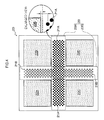
- Fig. 1 is a view showing the configuration of the semiconductor memory device in which the present invention is implemented.
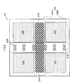
- Fig. 2 is a cross-sectional view of the Fig. 1 , A-A.
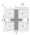
- Fig. 3 is a cross-sectional view of the Fig. 1 , B-B.
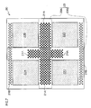
- Fig. 4 is a view showing the memory chip included in the semiconductor device in which the present invention is implemented.
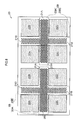
- the semiconductor device 100 is implemented as a flip chip where two units of memory chips 20 and the Application Specific Chip (hereinafter referred as "ASIC": the first semiconductor chip) 30 are implemented on the same main surface of the wiring chip 10 which serves as an interposer (mounted substrate).
- the two memory chips 20 and the ASIC 30 are disposed in such a way that each line of the two memory chips and one line of the ASIC 30 face with each other.
- the underfill resin 40 is filled between the wiring chip 10, the memory chips 20, and the ASIC 30.
- the underfill resin 42 is filled and stopped by the dam material 42A (material to stop the flow ofthe underfill resin) and the underfill resin 42 is disposed in such a way that it sticks out from the same main surface of the wiring chip 10 and surrounds the semiconductor chip implementation area (the implementation area of the memory chips 20 and the ASIC 30).
- the dam material 42A is shown in such a manner that it is disposed outside the semiconductor chip implementation area, but it can be disposed inside the semiconductor chip implementation area as well. However, the dam material 42A must be disposed outside the electrode group fabrication area.
- the wiring chip 10 is formed in such a manner that a plurality of metal wires (for example, aluminum or copper wires) are disposed on a silicon board, which is not indicated in the figures. And as shown in the Fig. 1-3 , one ends of such metal wires are connected to the connection pads 11A to implement memory chips 20 and the connection pads 11B to implement the ASIC 30, and the other ends of such metal wire are connected to the memory chips 20 and the ASIC 30, and the connection pads form a group.
- These connection pads 11A and 11B are made by conductive materials, such as aluminum.
- connection pads 11A and 11B of the wiring chip 10 are disposed along with the connection pads of the memory chips 20 and the ASIC 30 which are implemented. Needless to say, the connection pads 11A and 11B of the wiring chip 10 can be disposed either in a grid pattern, staggered pattern, or in other patterns in their disposition area, depending on the connection pads of the memory chips 20 and the ASIC 30 which are implemented.
- the wring pitch between the connection pads 11A and 11B of the wiring chip 10 is set as appropriate depending on the chips which are implemented.
- the bandwidth of the two units of 256M bit multimedia memories as the memory chips 20 and the ASIC 30 mentioned above.
- connection pads 11A and 11B of the wiring chip 10 also changes depending on the chips to be implemented. For example, this embodiment requires 2 units of 256M multimedia memory as the memory chips 20 and the ASIC 30, so the number of pads required is about 2500.
- the number of pads is not limited to 2500 and depending on the semiconductor chips which are implemented, the number of pads can be anywhere from 2000 to 5000 as appropriate.
- the wiring chip 10 comprises the same silicon board as the memory chips 20 and the ASIC 30. Therefore, it is highly resistant to heat, stretching and shrinking, and thus, reliable.
- the memory chips 20 are developed utilizing the semiconductor process technology on the silicon board, and while it is not indicated in the figures, for example, they are 256M bit multimedia memories for this embodiment.
- the memory chips 20 are not limited to the 256M bit multimedia memories but they can be general dynamic random access memories (DRAMs). Similarly, they can be static random access memories (SRAMs) or non-volatile memories.
- DRAMs general dynamic random access memories
- SRAMs static random access memories
- the memory chips comprises four divided memory banks 22A-22D (the first to fourth semiconductor circuit fabrication areas) in a rectangular shape on its main surface, and such memory banks 22A-22D comprise memory circuits (semiconductor circuits; not shown in the figures) which form memories.
- the memory circuit comprises a plurality of memory cells, each of which are connected to a plurality of bit lines and word lines, and access circuits which select a designated memory cell from the plurality of memory cells depending on the given address signal.
- the memory bank 22A and the memory bank 22B are disposed in such a manner so that one side of the memory bank 22A and one side of the memory bank 22B face with each other with a certain amount of distance.
- the memory bank 22A and the memory bank 22C are disposed in such a manner that the side of the memory bank 22A which crosses in the right angle with the side which faces with the memory bank 22B faces with one side of the memory bank 22C with a certain amount of distance.
- the memory bank 22B and the memory bank 22D are disposed in such a manner that the side of the memory bank 22B which crosses in the right angle with the side which faces with the memory bank 22A faces with one side of the memory bank 22D with a certain amount of distance.
- the memory bank 22C and the memory bank 22D are disposed in such a manner that the side of the memory bank 22C which crosses in the right angle with the side which faces with the memory bank 22A faces with one side of the memory bank 22D with a certain amount of distance.
- the memory banks 22A-22D are disposed in such a manner that two sides crossing in the right angle face with each other with a certain amount of space, and the entire memory banks 22A-22D are disposed along the edge of the main surface (along the shape of the memory chips 20, which is a rectangle) of the memory chips 20. And on the surface ofthe memory chips 20, there is a space which has a shape of a cross formed by each memory banks 22A-22D facing with each other with a certain amount of distance.
- connection bump disposition area 23 electrode disposition area
- connection bumps projecting electrodes
- the cross-shaped connection bump disposition area 23 is formed by the area 23A and 23B which cross with each other in the right angle.
- the area 23A is the area where the space set between the memory bank 22A and the memory bank 22B as well as the memory bank 22C and 22D stretches in the direction from the memory bank 22A and 22B (in the direction to the memory bank 22C and 22B) to the both edges of the main surface of the memory chips 20.
- the area 23B is the area where the space set between the memory bank 22A and 22C and the memory bank 22B and 22D stretches in the direction from the memory bank 22A and 22C (in the direction to the memory bank 22B and 22D) to the both edges of the main surface of the memory chips 20.
- the signal input/output connection bumps 21A (the first electrodes) of the memory chip 20 are disposed one after another in a group in the direction against the memory banks 22A and 22B (toward the direction of memory bank 22C and 22D).
- the disposition of the signal input/output connection bumps 21A can be either in a grid pattern or in a staggered pattern.
- the power/grounding connection bumps 21B are disposed one after another in a group, stretching in the direction against the memory banks 22A and 22C (toward the direction of memory bank 22B and 22D).
- These power/grounding connection bumps can be disposed either in a grid pattern, or in a staggered pattern.
- the signal input/output connection bumps 21A and the power/grounding connection bumps 21B are disposed in the cross-shaped connection bump disposition area 23, forming a group of connection bumps in a cross shape.
- the signal input/output connection bumps 21A and the power/grounding connection bumps 21B are disposed in such a manner that they have a certain amount of pitch between each bump. And it is recommended that the disposition pitch of the signal input/output connection bumps 21A (the number of bumps) is larger than the disposition pitch of the power/grounding connection bumps 21B (the number of bumps).
- the signal input/output connection bumps 21A (total number) in the area 23A are disposed as 13 (number in the width direction of the memory chips 20) x 122 (number in the direction of the elongated side of the memory chips 20) and the power/grounding connection bumps 21B (total number) are disposed as 8 (number in the width direction of the memory chips 20) x 103 (number in the direction of the elongated side of the memory chips 20).
- the memory chips 20 (memory circuit) and the wiring chip 10 as a flip chip. Also, by increasing the number of bumps (the number of pins), the power consumption and heat generation are reduced.
- each bump (signal input/output connection bumps 21A and the power/grounding connection bumps 21B) is disposed in such a manner that it has a certain distance from the edge of the memory banks (the side facing with the bump) toward outside (for example, the minimum distance is equal to or more than 150 ⁇ m and the minimum distance is indicated as "t" in the Fig. 3 from the edge).
- each bump receives any pressure from external shocks caused during implementation or from outside of the memory device, the memory banks are not affected by such pressure which may be conducted via such bumps. Also, as such, it is ensured that the memory banks are resistant against the a ray generated by each bump and the data stored in the memory cell formed in the memory banks is not inverted.
- pads are disposed for formation of such bumps as well as unit cell areas are disposed which includes input/output circuits which are electrically connected to such bumps.
- the I/O array in which the unit cell areas including input/output circuits are disposed in an array form is composed.
- the memory chip; 20 are disposed in such a manner that their connection pads configured as described above (signal input/output connection bumps 21A and the power/grounding connection bumps 21 B) are facing with the connection pads 11A of the wiring chip 10.
- the memory chips 20 are disposed in such a manner that respective electrodes (bumps and pads) of the memory chips 20 and the wiring chip 10 are facing with each other, physically connected with the soldering 40 as well as electrically connected, and implemented as a flip chip on top of the wiring chip 10.
- the memory chips 20 are implemented on top of the wiring chip 10 in such a manner that the area 23A is in parallel with the sides of memory chips 20 and the ASIC 30 which are facing with the area 23A.
- the structure of the wiring chip to electrically connect the memory chips 20 and the wiring chip 10 is simplified and connection problems can be avoided.
- each connection bump needs to be disposed on the both sides of the area 23A and the area 23B along its elongated sides, setting the center of these bumps as the center of the cross-shaped connection bump disposition area 23 (the area where the area 23A and 23B overlap with each other),and preferably, disposed symmetrically.
- the ASIC 30 is developed utilizing the semiconductor process technology on the silicon board, and for example, a logic circuit including a general-purpose CPU is adopoted.
- the input output bit number of the ASIC 30 is 512 bit, corresponding to the 2.1GB/seconds. Needless to say, depending on the performance of the memory chips 20 (such as their bandwidth), the input output bit number can be higher.
- the ASIC 30 is not limited to a logic circuit as mentioned above, but it can also utilize a general-purpose analog circuit, such as the one including an A/D converter which converts analog signals to digital signals.
- connection bumps 31 are disposed in such a way along the edge, forming a group, facing with the memory chips 20.
- These power/grounding connection bumps 21B can be disposed either in a grid pattern or in a staggered pattern.
- the ASIC 30 is disposed in such a manner that its connection bumps 31 face with the connection pads 11B of the wiring chip 10.
- the ASIC 30 and the wiring chip 10 are disposed in such a manner that their respective electrodes (pads and bumps) are facing with each other, physically connected with the soldering 40 as well as electrically connected, thus the ASIC 30 is implemented as a flip chip on top of the wiring chip 10.
- the memory chips 20 and the ASIC 30 are connected electrically and physically via metal wires (not shown in figures) connected to the connection pads of the wiring chip 10. Since ASIC 30 is electrically connected with two units of 256 bit multi media memories which are the memory chips 20, the input and output of signals are conducted in parallel in 512 bit chunks.
- connection bump of memory chips 20 By connecting each connection bump of memory chips 20 with each connection bump of the ASIC 30 electrically via metal wires (not shown in figures) connected to the connection pads of the wiring chip 10, a bus line connection is realized.
- the wiring chip 10 comprises connection pads for external connection and by electrically connecting their connection wires, the memory device 100 is connected to outside.
- the main surface of the memory chips are divided into four areas in which the memory circuits (semiconductor circuits; not shown in the figures) are formed, and these four areas are facing with each other with their two sides crossing in the right angles facing with each other with a certain amount of distance, shaping four of rectangular-shaped memory banks 22A-22D. Therefore, in the middle of the memory chips 20, there is a cross-shaped connection bump disposition area 23 which is formed by the memory banks 22A-22D which face with each other with a certain amount of distance. And in the area 23A in the cross-shaped connection bump disposition area 23, the signal input/output connection bumps 21A (the first electrc des) are disposed in a group. In short, the signal input/output connection bumps 21A are collectively disposed in a certain area, thus, the formation of signal input/output wiring to the divided semiconductor circuits is efficient and the space which electrodes occupy on the semiconductor chip is minimized.
- a group of power/grounding connection bumps 21B is disposed in the area 23B which crosses in the right angle with the area 23A where the signal input/output bumps 21A are disposed in a group form.
- the memory chips 20 are supported (via soldering) by the power/grounding connection bumps 21 B of the memory chips 20 so that the memory chips 20 do not tilt toward the crossing direction along the elongated side of the group of signal input/output connection bumps 21A of the memory chips 20, and the memory chips 20 are supported (via soldering) by the signal input/output connection bumps 21A so that the memory chips 20 do not tilt in the crossing direction along the elongated side of the power/grounding connection bumps 21B.
- the memory chips 20 are disposed in such a manner that they have a certain distance from the wiring chip 10.
- the memory chips 20 and the wiring chip 10 face with each other in parallel. If the distance between the memory chips 20 and the wiring chip 10 is 20-30 ⁇ m, it means that the space margin between the memory chips 20 and the wiring chip 10 is within from ⁇ 3 ⁇ m to ⁇ 4 ⁇ m range in terms ofthe entire area where the chips are facing with each other.
- the parallel implementation of the memory chips 20 and the wiring chip 10 can be maintained with a minimum number of bumps.
- the power/grounding connection bumps 21B for maintaining the parallel position are disposed in the non-fabrication area of the memory banks, it can be prevented that the memory circuit is damaged by a physical pressure caused when implementing the memory chips 20 onto the wiring chip 10. Also since the power/grounding connection bumps 21B are utilized to maintain the parallel position, connection to the power source and grounding are also strongly enforced.
- the underfill resin 42 is filled between the memory chips 20 and the wiring chip 10 without the existence of any group of electrodes in the fabrication area of the memory bank. Also, since the memory banks of the memory chips 20 do not have any group of electrodes, there is no possibility of defects caused by the fill, and it is easy to fill the space completely with the underfill resin 42. As a result, the underfill resin 42 absorbs physical shocks sufficiently, thus the memory chips 20 are less likely to be damaged by physical shocks to the memory banks.
- a group of the power/grounding connection bumps 21B is disposed in the area 23B which crosses with the area 23A in the right angle where there is a group of the signal input/output connection bumps 21A; in other words, it is disposed in the center space which is formed by the rectangular-shaped memory banks 22A-22D, making a group of the power/grounding connection bumps 21B the closest to each memory bank, thus supplying power and grounding to memory circuits (cells) formed in each memory bank evenly with the shortest wiring.
- the number of electrodes (bumps) of the memory chips 20 are kept minimum, the parallel position of the memory chips 20 to the mounted substrate (wiring chip 10) is maintained, thus avoiding connection problems and preventing the semiconductor circuit (memory circuit) from being damaged.
- the composition of a memory chip having a group of power/grounding connection bumps 21 B in the area 23B ofthe cross-shaped connection bump disposition area 23 as bumps (electrodes) to maintain a parallel implementation is explained, but the present invention is not limited to this composition.
- the present invention can be the group of power/grounding connection bumps 21B, some of which are disposed densely and some of which are disposed thinly, in the area 23B of the cross-shaped connection bump disposition area 23.
- the composition of a memory chip utilizing a group of power/grounding connection bumps 21 B in the area 23B of the cross-shaped connection bump disposition area 23 as bumps (electrodes) to maintain a parallel implementation is explained, but the present invention is not limited to this composition.
- signal input/output connection bumps or dummy bumps can be utilized in stead of the power/grounding connection bumps 21B.
- a group of signal input/output connection bumps 21A which are disposed in the area 23A (where it overlaps with the area 23B) can be aligned continuously to the group of signal input/output connection bumps 21A which is disposed in the area 23B in the cross-shaped bump disposition area 23.
- the signal input/output connection bumps 21A are disposed from the center of the chip to the center of each memory bank which is facing with each other.
- a group of power/grounding connection bumps 218 is disposed on the both edges of the area 23B toward its elongated sides (on the both edges of the chip).
- the composition of memory chips 20 comprising four divided memory banks 22A-22D which are disposed near the edges of the chip, but the present invention is not limited to this composition.
- the composition can be in such a way that there is a certain space between the memory bank 22 and the edge of the chip. In concrete, for example, as shown in the Fig.
- each memory bank can be disposed in such a manner that the memory bank 22A and the memory bank 22B have a certain space from the edge of the memory chip 20 (the edge toward the direction of the elongated sides of the area 23B) and similarly, the memory bank 22C and 22 have a certain space from the other edge of the memory chip 20 (the other side of the edge toward the direction of the elongated sides of the area 23B), and the power/grounding connection bumps 21B can be disposed in the spaces formed on the both edges.
- the power/grounding connection bumps 21 B which are disposed ir such spaces on such edges are disposed with a certain amount of distance from the edge of the memory bank (the side facing with the bumps) toward outside (for example, equal to or more than min mum 150 ⁇ m from the edges: the minimum distance is shown as "t" in the Fig. 3 ).
- the composition of this case is the same is the composition shown in the Fig. 6 .
- the composition of four memory banks was explained, but the present invention is not limited to this composition.
- the present invention is not limited to this composition.
- connection bumps in the cross-shaped connection bump disposition area 23 on the memory chips 20 is explained, but the present invention is not limited to this composition.
- the same method can be applied to the ASIC 30 which is divided into four logic circuits (semiconductor circuits).
- a composition to implement memory chips 20 and the ASIC 30 on the same main surface of the wiring chip 10 which is an interposer (mounted substrate) as a flip chip is explained, but an ASIC chip can be used in stead of the wiring chip 10 and it is possible to implement them as a COC (chip-on-chip) to compose a semiconductor device.
- COC chip-on-chip
- the semiconductor device 101 in which a memory chip 20 is implemented on the main surface of the ASIC 30 as a flip chip is an example.
- a group of electrodes of the ASIC 30 (connection bumps) are disposed in the same manner as a group of electrodes of the memory chip 20 (connection bumps).
Landscapes
- Semiconductor Integrated Circuits (AREA)
- Semiconductor Memories (AREA)
- Wire Bonding (AREA)
- Internal Circuitry In Semiconductor Integrated Circuit Devices (AREA)
Applications Claiming Priority (2)
| Application Number | Priority Date | Filing Date | Title |
|---|---|---|---|
| JP2008037452A JP2009200101A (ja) | 2008-02-19 | 2008-02-19 | 半導体チップ及び半導体装置 |
| PCT/JP2009/052493 WO2009104536A1 (ja) | 2008-02-19 | 2009-02-16 | 半導体チップ及び半導体装置 |
Publications (2)
| Publication Number | Publication Date |
|---|---|
| EP2249381A1 true EP2249381A1 (de) | 2010-11-10 |
| EP2249381A4 EP2249381A4 (de) | 2012-11-21 |
Family
ID=40985417
Family Applications (1)
| Application Number | Title | Priority Date | Filing Date |
|---|---|---|---|
| EP09712660A Withdrawn EP2249381A4 (de) | 2008-02-19 | 2009-02-16 | Halbleiterchip und halbleiteranordnung |
Country Status (7)
| Country | Link |
|---|---|
| US (1) | US20100327457A1 (de) |
| EP (1) | EP2249381A4 (de) |
| JP (1) | JP2009200101A (de) |
| KR (1) | KR20100123860A (de) |
| CN (1) | CN101952956A (de) |
| TW (1) | TW201001670A (de) |
| WO (1) | WO2009104536A1 (de) |
Families Citing this family (39)
| Publication number | Priority date | Publication date | Assignee | Title |
|---|---|---|---|---|
| JP2009295740A (ja) * | 2008-06-04 | 2009-12-17 | Elpida Memory Inc | メモリチップ及び半導体装置 |
| JP5342422B2 (ja) * | 2009-12-10 | 2013-11-13 | ルネサスエレクトロニクス株式会社 | 半導体装置およびその製造方法 |
| US8796863B2 (en) * | 2010-02-09 | 2014-08-05 | Samsung Electronics Co., Ltd. | Semiconductor memory devices and semiconductor packages |
| US8901747B2 (en) | 2010-07-29 | 2014-12-02 | Mosys, Inc. | Semiconductor chip layout |
| KR20120056018A (ko) * | 2010-11-24 | 2012-06-01 | 삼성전자주식회사 | 범프들과 테스트 패드들이 십자 모양으로 배열되는 반도체 장치 |
| KR101262638B1 (ko) | 2010-12-06 | 2013-05-08 | 기아자동차주식회사 | 엘피아이 연료시스템용 솔레노이드 밸브 |
| JP5579108B2 (ja) | 2011-03-16 | 2014-08-27 | 株式会社東芝 | 半導体装置 |
| US8823165B2 (en) | 2011-07-12 | 2014-09-02 | Invensas Corporation | Memory module in a package |
| US8513817B2 (en) | 2011-07-12 | 2013-08-20 | Invensas Corporation | Memory module in a package |
| US8502390B2 (en) | 2011-07-12 | 2013-08-06 | Tessera, Inc. | De-skewed multi-die packages |
| US8659140B2 (en) | 2011-10-03 | 2014-02-25 | Invensas Corporation | Stub minimization using duplicate sets of signal terminals in assemblies without wirebonds to package substrate |
| KR101840240B1 (ko) * | 2011-10-03 | 2018-05-04 | 인벤사스 코포레이션 | 마이크로 전자 패키지 |
| US8659142B2 (en) | 2011-10-03 | 2014-02-25 | Invensas Corporation | Stub minimization for wirebond assemblies without windows |
| US8629545B2 (en) | 2011-10-03 | 2014-01-14 | Invensas Corporation | Stub minimization for assemblies without wirebonds to package substrate |
| TWI515864B (zh) | 2011-10-03 | 2016-01-01 | 英帆薩斯公司 | 具有自封裝中心偏移之端子格柵之短線最小化 |
| KR101894823B1 (ko) | 2011-10-03 | 2018-09-04 | 인벤사스 코포레이션 | 평행한 윈도우를 갖는 다중-다이 와이어 본드 어셈블리를 위한 스터브 최소화 |
| US8436457B2 (en) | 2011-10-03 | 2013-05-07 | Invensas Corporation | Stub minimization for multi-die wirebond assemblies with parallel windows |
| KR20140085497A (ko) | 2011-10-03 | 2014-07-07 | 인벤사스 코포레이션 | 직교 윈도가 있는 멀티-다이 와이어본드 어셈블리를 위한 스터브 최소화 |
| US8659141B2 (en) | 2011-10-03 | 2014-02-25 | Invensas Corporation | Stub minimization using duplicate sets of terminals for wirebond assemblies without windows |
| US8441111B2 (en) | 2011-10-03 | 2013-05-14 | Invensas Corporation | Stub minimization for multi-die wirebond assemblies with parallel windows |
| US8759163B2 (en) * | 2012-04-30 | 2014-06-24 | Taiwan Semiconductor Manufacturing Co., Ltd. | Layout of a MOS array edge with density gradient smoothing |
| US9006908B2 (en) * | 2012-08-01 | 2015-04-14 | Marvell Israel (M.I.S.L) Ltd. | Integrated circuit interposer and method of manufacturing the same |
| US8848392B2 (en) | 2012-08-27 | 2014-09-30 | Invensas Corporation | Co-support module and microelectronic assembly |
| US8848391B2 (en) | 2012-08-27 | 2014-09-30 | Invensas Corporation | Co-support component and microelectronic assembly |
| US8787034B2 (en) | 2012-08-27 | 2014-07-22 | Invensas Corporation | Co-support system and microelectronic assembly |
| US9368477B2 (en) | 2012-08-27 | 2016-06-14 | Invensas Corporation | Co-support circuit panel and microelectronic packages |
| US20140159238A1 (en) * | 2012-12-07 | 2014-06-12 | Qualcomm Incorporated | Package having thermal compression flip chip (tcfc) and chip with reflow bonding on lead |
| KR101324431B1 (ko) * | 2013-05-14 | 2013-10-31 | 주식회사 한국인삼공사 | 숙취해소용 조성물 |
| US9070423B2 (en) | 2013-06-11 | 2015-06-30 | Invensas Corporation | Single package dual channel memory with co-support |
| US9123555B2 (en) | 2013-10-25 | 2015-09-01 | Invensas Corporation | Co-support for XFD packaging |
| US9305131B2 (en) * | 2013-12-03 | 2016-04-05 | Mediatek Inc. | Method for flip chip packaging co-design |
| US9281296B2 (en) | 2014-07-31 | 2016-03-08 | Invensas Corporation | Die stacking techniques in BGA memory package for small footprint CPU and memory motherboard design |
| US9691437B2 (en) | 2014-09-25 | 2017-06-27 | Invensas Corporation | Compact microelectronic assembly having reduced spacing between controller and memory packages |
| US9659863B2 (en) * | 2014-12-01 | 2017-05-23 | Taiwan Semiconductor Manufacturing Company, Ltd. | Semiconductor devices, multi-die packages, and methods of manufacture thereof |
| US9543192B2 (en) * | 2015-05-18 | 2017-01-10 | Globalfoundries Singapore Pte. Ltd. | Stitched devices |
| US9484080B1 (en) | 2015-11-09 | 2016-11-01 | Invensas Corporation | High-bandwidth memory application with controlled impedance loading |
| US9679613B1 (en) | 2016-05-06 | 2017-06-13 | Invensas Corporation | TFD I/O partition for high-speed, high-density applications |
| US20230326819A1 (en) * | 2022-04-12 | 2023-10-12 | Taiwan Semiconductor Manufacturing Company Limited | Dam structure for integrated passive device integration and methods of forming the same |
| US20230420298A1 (en) * | 2022-06-28 | 2023-12-28 | Intel Corporation | Multi-pathway routing via through hole |
Family Cites Families (23)
| Publication number | Priority date | Publication date | Assignee | Title |
|---|---|---|---|---|
| JPH0562978A (ja) * | 1991-08-30 | 1993-03-12 | Fujitsu Ltd | フリツプチツプ |
| JP3226703B2 (ja) | 1994-03-18 | 2001-11-05 | 株式会社日立製作所 | 半導体装置及びその製法 |
| JP2006157047A (ja) * | 1995-03-30 | 2006-06-15 | Renesas Technology Corp | 半導体パッケージ |
| JP3494502B2 (ja) * | 1995-05-12 | 2004-02-09 | 株式会社ルネサステクノロジ | 半導体記憶装置およびそのパッド配置方法 |
| US20040061220A1 (en) * | 1996-03-22 | 2004-04-01 | Chuichi Miyazaki | Semiconductor device and manufacturing method thereof |
| US5719449A (en) * | 1996-09-30 | 1998-02-17 | Lucent Technologies Inc. | Flip-chip integrated circuit with improved testability |
| WO1998035293A1 (fr) * | 1997-02-07 | 1998-08-13 | T.I.F. Co., Ltd. | Systeme de memoire |
| JPH1131716A (ja) * | 1997-07-11 | 1999-02-02 | Hitachi Ltd | 半導体装置の製造方法及び半導体チップ |
| JP3259763B2 (ja) * | 1997-11-14 | 2002-02-25 | 日本電気株式会社 | 半導体lsi |
| JP3557114B2 (ja) | 1998-12-22 | 2004-08-25 | 株式会社東芝 | 半導体記憶装置 |
| JP2000315776A (ja) | 1999-05-06 | 2000-11-14 | Hitachi Ltd | 半導体装置 |
| JP3469168B2 (ja) | 2000-07-05 | 2003-11-25 | 新光電気工業株式会社 | 配線基板及び半導体装置 |
| JP2003258154A (ja) | 2002-03-05 | 2003-09-12 | Fujitsu Ltd | 半導体素子の実装構造 |
| JP2004063753A (ja) * | 2002-07-29 | 2004-02-26 | Nec Kansai Ltd | チップオンチップ接続用半導体チップ及びその接続方法 |
| JP4776861B2 (ja) * | 2002-09-26 | 2011-09-21 | ルネサスエレクトロニクス株式会社 | 半導体装置 |
| JP2004265940A (ja) * | 2003-02-19 | 2004-09-24 | Sony Corp | 半導体装置 |
| JP3722224B2 (ja) * | 2003-12-24 | 2005-11-30 | セイコーエプソン株式会社 | 半導体チップ及び半導体装置並びに半導体装置の製造方法 |
| DE102004014018B3 (de) | 2004-03-19 | 2005-08-11 | Forschungsverbund Berlin E.V. | Mikrowellenantenne für in Flip-Chip-Technologie hergestellte Halbleiterbaugruppen |
| US7015592B2 (en) * | 2004-03-19 | 2006-03-21 | Intel Corporation | Marking on underfill |
| DE102004042073A1 (de) * | 2004-08-31 | 2006-03-09 | Infineon Technologies Ag | Schaltungsanordnung zur Datenspeicherung |
| JP2006147629A (ja) | 2004-11-16 | 2006-06-08 | Matsushita Electric Works Ltd | 半導体装置およびその評価方法 |
| US7684781B2 (en) * | 2005-11-25 | 2010-03-23 | Semiconductor Energy Laboratory Co., Ltd | Semiconductor device |
| JP2008066371A (ja) * | 2006-09-05 | 2008-03-21 | Matsushita Electric Ind Co Ltd | 半導体集積回路における電源配線構造 |
-
2008
- 2008-02-19 JP JP2008037452A patent/JP2009200101A/ja active Pending
-
2009
- 2009-02-16 TW TW098104879A patent/TW201001670A/zh unknown
- 2009-02-16 US US12/918,401 patent/US20100327457A1/en not_active Abandoned
- 2009-02-16 WO PCT/JP2009/052493 patent/WO2009104536A1/ja not_active Ceased
- 2009-02-16 CN CN2009801057659A patent/CN101952956A/zh active Pending
- 2009-02-16 KR KR1020107019920A patent/KR20100123860A/ko not_active Ceased
- 2009-02-16 EP EP09712660A patent/EP2249381A4/de not_active Withdrawn
Also Published As
| Publication number | Publication date |
|---|---|
| KR20100123860A (ko) | 2010-11-25 |
| CN101952956A (zh) | 2011-01-19 |
| US20100327457A1 (en) | 2010-12-30 |
| JP2009200101A (ja) | 2009-09-03 |
| TW201001670A (en) | 2010-01-01 |
| WO2009104536A1 (ja) | 2009-08-27 |
| EP2249381A4 (de) | 2012-11-21 |
Similar Documents
| Publication | Publication Date | Title |
|---|---|---|
| EP2249381A1 (de) | Halbleiterchip und halbleiteranordnung | |
| US7944036B2 (en) | Semiconductor device including mounting board with stitches and first and second semiconductor chips | |
| US9496243B2 (en) | Microelectronic assembly with opposing microelectronic packages each having terminals with signal assignments that mirror each other with respect to a central axis | |
| US9281271B2 (en) | Stub minimization using duplicate sets of signal terminals having modulo-x symmetry in assemblies without wirebonds to package substrate | |
| US7598617B2 (en) | Stack package utilizing through vias and re-distribution lines | |
| JP2013197387A (ja) | 半導体装置 | |
| TWI761632B (zh) | 包含與半導體晶粒分隔開的橋式晶粒之半導體封裝 | |
| US7771206B2 (en) | Horizontal dual in-line memory modules | |
| JP2009141312A (ja) | スタック型チップパッケージ構造 | |
| TW202101726A (zh) | 具有中介件的堆疊半導體封裝件 | |
| EP2764547B1 (de) | Stub-minimierung mit duplizierten sätzen von endgeräten für drahtgebundene anordnungen ohne fenster | |
| CN114121873A (zh) | 具有球栅阵列的设备和系统及相关微电子装置和装置封装 | |
| JP4707446B2 (ja) | 半導体装置 | |
| US6777815B2 (en) | Configuration of conductive bumps and redistribution layer on a flip chip | |
| JP5288892B2 (ja) | スタックモジュール、及びそれを備えるカード及びシステム | |
| US8304879B2 (en) | Spiral staircase shaped stacked semiconductor package and method for manufacturing the same | |
| JP2015109408A (ja) | 複合チップ、半導体装置、及び半導体装置の製造方法 | |
| KR102426664B1 (ko) | 범프 패드들을 가지는 집적 회로 및 그것을 포함하는 반도체 패키지 | |
| JP4658529B2 (ja) | 集積回路モジュールの構造 | |
| JP3813768B2 (ja) | 半導体装置及び半導体モジュール | |
| EP4123695A1 (de) | Gestapeltes gehäuse für speicherchip und elektronische vorrichtung | |
| TWI886838B (zh) | 電子裝置 | |
| KR102891268B1 (ko) | 팬-아웃형 적층 패키지, 이의 제조방법 및 이를 포함하는 전자 장치 | |
| KR102937174B1 (ko) | 적층 패키지, 이의 제조방법 및 이를 포함하는 전자 장치 | |
| TWI864514B (zh) | 記憶體模組 |
Legal Events
| Date | Code | Title | Description |
|---|---|---|---|
| PUAI | Public reference made under article 153(3) epc to a published international application that has entered the european phase |
Free format text: ORIGINAL CODE: 0009012 |
|
| 17P | Request for examination filed |
Effective date: 20100909 |
|
| AK | Designated contracting states |
Kind code of ref document: A1 Designated state(s): AT BE BG CH CY CZ DE DK EE ES FI FR GB GR HR HU IE IS IT LI LT LU LV MC MK MT NL NO PL PT RO SE SI SK TR |
|
| AX | Request for extension of the european patent |
Extension state: AL BA RS |
|
| DAX | Request for extension of the european patent (deleted) | ||
| A4 | Supplementary search report drawn up and despatched |
Effective date: 20121019 |
|
| RIC1 | Information provided on ipc code assigned before grant |
Ipc: H01L 23/50 20060101AFI20121015BHEP Ipc: H01L 23/485 20060101ALI20121015BHEP Ipc: H01L 21/60 20060101ALI20121015BHEP Ipc: H01L 25/18 20060101ALN20121015BHEP |
|
| STAA | Information on the status of an ep patent application or granted ep patent |
Free format text: STATUS: THE APPLICATION IS DEEMED TO BE WITHDRAWN |
|
| 18D | Application deemed to be withdrawn |
Effective date: 20130517 |