EP2248165B1 - Process of grounding heat spreader/stiffener to a flip chip package using solder and film adhesive - Google Patents
Process of grounding heat spreader/stiffener to a flip chip package using solder and film adhesive Download PDFInfo
- Publication number
- EP2248165B1 EP2248165B1 EP08872772.2A EP08872772A EP2248165B1 EP 2248165 B1 EP2248165 B1 EP 2248165B1 EP 08872772 A EP08872772 A EP 08872772A EP 2248165 B1 EP2248165 B1 EP 2248165B1
- Authority
- EP
- European Patent Office
- Prior art keywords
- holes
- stiffener
- substrate
- solder
- heat spreader
- Prior art date
- Legal status (The legal status is an assumption and is not a legal conclusion. Google has not performed a legal analysis and makes no representation as to the accuracy of the status listed.)
- Active
Links
Images

Classifications
-
- H—ELECTRICITY
- H01—ELECTRIC ELEMENTS
- H01L—SEMICONDUCTOR DEVICES NOT COVERED BY CLASS H10
- H01L23/00—Details of semiconductor or other solid state devices
- H01L23/48—Arrangements for conducting electric current to or from the solid state body in operation, e.g. leads, terminal arrangements ; Selection of materials therefor
- H01L23/50—Arrangements for conducting electric current to or from the solid state body in operation, e.g. leads, terminal arrangements ; Selection of materials therefor for integrated circuit devices, e.g. power bus, number of leads
-
- H—ELECTRICITY
- H01—ELECTRIC ELEMENTS
- H01L—SEMICONDUCTOR DEVICES NOT COVERED BY CLASS H10
- H01L23/00—Details of semiconductor or other solid state devices
- H01L23/02—Containers; Seals
- H01L23/10—Containers; Seals characterised by the material or arrangement of seals between parts, e.g. between cap and base of the container or between leads and walls of the container
-
- H—ELECTRICITY
- H01—ELECTRIC ELEMENTS
- H01L—SEMICONDUCTOR DEVICES NOT COVERED BY CLASS H10
- H01L23/00—Details of semiconductor or other solid state devices
- H01L23/34—Arrangements for cooling, heating, ventilating or temperature compensation ; Temperature sensing arrangements
- H01L23/36—Selection of materials, or shaping, to facilitate cooling or heating, e.g. heatsinks
-
- H—ELECTRICITY
- H01—ELECTRIC ELEMENTS
- H01L—SEMICONDUCTOR DEVICES NOT COVERED BY CLASS H10
- H01L23/00—Details of semiconductor or other solid state devices
- H01L23/48—Arrangements for conducting electric current to or from the solid state body in operation, e.g. leads, terminal arrangements ; Selection of materials therefor
- H01L23/488—Arrangements for conducting electric current to or from the solid state body in operation, e.g. leads, terminal arrangements ; Selection of materials therefor consisting of soldered or bonded constructions
- H01L23/498—Leads, i.e. metallisations or lead-frames on insulating substrates, e.g. chip carriers
- H01L23/49833—Leads, i.e. metallisations or lead-frames on insulating substrates, e.g. chip carriers the chip support structure consisting of a plurality of insulating substrates
-
- H—ELECTRICITY
- H01—ELECTRIC ELEMENTS
- H01L—SEMICONDUCTOR DEVICES NOT COVERED BY CLASS H10
- H01L23/00—Details of semiconductor or other solid state devices
- H01L23/552—Protection against radiation, e.g. light or electromagnetic waves
-
- H—ELECTRICITY
- H01—ELECTRIC ELEMENTS
- H01L—SEMICONDUCTOR DEVICES NOT COVERED BY CLASS H10
- H01L2224/00—Indexing scheme for arrangements for connecting or disconnecting semiconductor or solid-state bodies and methods related thereto as covered by H01L24/00
- H01L2224/01—Means for bonding being attached to, or being formed on, the surface to be connected, e.g. chip-to-package, die-attach, "first-level" interconnects; Manufacturing methods related thereto
- H01L2224/10—Bump connectors; Manufacturing methods related thereto
- H01L2224/15—Structure, shape, material or disposition of the bump connectors after the connecting process
- H01L2224/16—Structure, shape, material or disposition of the bump connectors after the connecting process of an individual bump connector
- H01L2224/161—Disposition
- H01L2224/16151—Disposition the bump connector connecting between a semiconductor or solid-state body and an item not being a semiconductor or solid-state body, e.g. chip-to-substrate, chip-to-passive
- H01L2224/16221—Disposition the bump connector connecting between a semiconductor or solid-state body and an item not being a semiconductor or solid-state body, e.g. chip-to-substrate, chip-to-passive the body and the item being stacked
- H01L2224/16225—Disposition the bump connector connecting between a semiconductor or solid-state body and an item not being a semiconductor or solid-state body, e.g. chip-to-substrate, chip-to-passive the body and the item being stacked the item being non-metallic, e.g. insulating substrate with or without metallisation
-
- H—ELECTRICITY
- H01—ELECTRIC ELEMENTS
- H01L—SEMICONDUCTOR DEVICES NOT COVERED BY CLASS H10
- H01L2224/00—Indexing scheme for arrangements for connecting or disconnecting semiconductor or solid-state bodies and methods related thereto as covered by H01L24/00
- H01L2224/01—Means for bonding being attached to, or being formed on, the surface to be connected, e.g. chip-to-package, die-attach, "first-level" interconnects; Manufacturing methods related thereto
- H01L2224/26—Layer connectors, e.g. plate connectors, solder or adhesive layers; Manufacturing methods related thereto
- H01L2224/31—Structure, shape, material or disposition of the layer connectors after the connecting process
- H01L2224/32—Structure, shape, material or disposition of the layer connectors after the connecting process of an individual layer connector
- H01L2224/321—Disposition
- H01L2224/32151—Disposition the layer connector connecting between a semiconductor or solid-state body and an item not being a semiconductor or solid-state body, e.g. chip-to-substrate, chip-to-passive
- H01L2224/32221—Disposition the layer connector connecting between a semiconductor or solid-state body and an item not being a semiconductor or solid-state body, e.g. chip-to-substrate, chip-to-passive the body and the item being stacked
- H01L2224/32225—Disposition the layer connector connecting between a semiconductor or solid-state body and an item not being a semiconductor or solid-state body, e.g. chip-to-substrate, chip-to-passive the body and the item being stacked the item being non-metallic, e.g. insulating substrate with or without metallisation
-
- H—ELECTRICITY
- H01—ELECTRIC ELEMENTS
- H01L—SEMICONDUCTOR DEVICES NOT COVERED BY CLASS H10
- H01L2224/00—Indexing scheme for arrangements for connecting or disconnecting semiconductor or solid-state bodies and methods related thereto as covered by H01L24/00
- H01L2224/73—Means for bonding being of different types provided for in two or more of groups H01L2224/10, H01L2224/18, H01L2224/26, H01L2224/34, H01L2224/42, H01L2224/50, H01L2224/63, H01L2224/71
- H01L2224/732—Location after the connecting process
- H01L2224/73201—Location after the connecting process on the same surface
- H01L2224/73203—Bump and layer connectors
- H01L2224/73204—Bump and layer connectors the bump connector being embedded into the layer connector
-
- H—ELECTRICITY
- H01—ELECTRIC ELEMENTS
- H01L—SEMICONDUCTOR DEVICES NOT COVERED BY CLASS H10
- H01L2224/00—Indexing scheme for arrangements for connecting or disconnecting semiconductor or solid-state bodies and methods related thereto as covered by H01L24/00
- H01L2224/73—Means for bonding being of different types provided for in two or more of groups H01L2224/10, H01L2224/18, H01L2224/26, H01L2224/34, H01L2224/42, H01L2224/50, H01L2224/63, H01L2224/71
- H01L2224/732—Location after the connecting process
- H01L2224/73251—Location after the connecting process on different surfaces
- H01L2224/73253—Bump and layer connectors
-
- H—ELECTRICITY
- H01—ELECTRIC ELEMENTS
- H01L—SEMICONDUCTOR DEVICES NOT COVERED BY CLASS H10
- H01L24/00—Arrangements for connecting or disconnecting semiconductor or solid-state bodies; Methods or apparatus related thereto
- H01L24/01—Means for bonding being attached to, or being formed on, the surface to be connected, e.g. chip-to-package, die-attach, "first-level" interconnects; Manufacturing methods related thereto
- H01L24/10—Bump connectors ; Manufacturing methods related thereto
- H01L24/15—Structure, shape, material or disposition of the bump connectors after the connecting process
- H01L24/16—Structure, shape, material or disposition of the bump connectors after the connecting process of an individual bump connector
-
- H—ELECTRICITY
- H01—ELECTRIC ELEMENTS
- H01L—SEMICONDUCTOR DEVICES NOT COVERED BY CLASS H10
- H01L2924/00—Indexing scheme for arrangements or methods for connecting or disconnecting semiconductor or solid-state bodies as covered by H01L24/00
- H01L2924/01—Chemical elements
- H01L2924/01057—Lanthanum [La]
-
- H—ELECTRICITY
- H01—ELECTRIC ELEMENTS
- H01L—SEMICONDUCTOR DEVICES NOT COVERED BY CLASS H10
- H01L2924/00—Indexing scheme for arrangements or methods for connecting or disconnecting semiconductor or solid-state bodies as covered by H01L24/00
- H01L2924/01—Chemical elements
- H01L2924/01079—Gold [Au]
-
- H—ELECTRICITY
- H01—ELECTRIC ELEMENTS
- H01L—SEMICONDUCTOR DEVICES NOT COVERED BY CLASS H10
- H01L2924/00—Indexing scheme for arrangements or methods for connecting or disconnecting semiconductor or solid-state bodies as covered by H01L24/00
- H01L2924/10—Details of semiconductor or other solid state devices to be connected
- H01L2924/11—Device type
- H01L2924/14—Integrated circuits
-
- H—ELECTRICITY
- H01—ELECTRIC ELEMENTS
- H01L—SEMICONDUCTOR DEVICES NOT COVERED BY CLASS H10
- H01L2924/00—Indexing scheme for arrangements or methods for connecting or disconnecting semiconductor or solid-state bodies as covered by H01L24/00
- H01L2924/15—Details of package parts other than the semiconductor or other solid state devices to be connected
- H01L2924/151—Die mounting substrate
- H01L2924/1515—Shape
- H01L2924/15153—Shape the die mounting substrate comprising a recess for hosting the device
-
- H—ELECTRICITY
- H01—ELECTRIC ELEMENTS
- H01L—SEMICONDUCTOR DEVICES NOT COVERED BY CLASS H10
- H01L2924/00—Indexing scheme for arrangements or methods for connecting or disconnecting semiconductor or solid-state bodies as covered by H01L24/00
- H01L2924/15—Details of package parts other than the semiconductor or other solid state devices to be connected
- H01L2924/151—Die mounting substrate
- H01L2924/1517—Multilayer substrate
-
- H—ELECTRICITY
- H01—ELECTRIC ELEMENTS
- H01L—SEMICONDUCTOR DEVICES NOT COVERED BY CLASS H10
- H01L2924/00—Indexing scheme for arrangements or methods for connecting or disconnecting semiconductor or solid-state bodies as covered by H01L24/00
- H01L2924/15—Details of package parts other than the semiconductor or other solid state devices to be connected
- H01L2924/151—Die mounting substrate
- H01L2924/153—Connection portion
- H01L2924/1531—Connection portion the connection portion being formed only on the surface of the substrate opposite to the die mounting surface
- H01L2924/15311—Connection portion the connection portion being formed only on the surface of the substrate opposite to the die mounting surface being a ball array, e.g. BGA
-
- H—ELECTRICITY
- H01—ELECTRIC ELEMENTS
- H01L—SEMICONDUCTOR DEVICES NOT COVERED BY CLASS H10
- H01L2924/00—Indexing scheme for arrangements or methods for connecting or disconnecting semiconductor or solid-state bodies as covered by H01L24/00
- H01L2924/15—Details of package parts other than the semiconductor or other solid state devices to be connected
- H01L2924/161—Cap
- H01L2924/1615—Shape
- H01L2924/16195—Flat cap [not enclosing an internal cavity]
-
- H—ELECTRICITY
- H01—ELECTRIC ELEMENTS
- H01L—SEMICONDUCTOR DEVICES NOT COVERED BY CLASS H10
- H01L2924/00—Indexing scheme for arrangements or methods for connecting or disconnecting semiconductor or solid-state bodies as covered by H01L24/00
- H01L2924/30—Technical effects
- H01L2924/301—Electrical effects
- H01L2924/3025—Electromagnetic shielding
Definitions
- the present invention relates to semiconductor chip assembly generally and, more particularly, to a method and/or architecture for grounding a heat spreader/stiffener to a flip chip package using solder and film adhesive.
- heat sink and/or heat spreader Conventional package grounding for electromagnetic shielding is done via a heat sink and/or heat spreader.
- the heat sink and/or heat spreader are connected to a printed circuit board (PCB) using clamps, wires, or some other connecting means.
- PCB printed circuit board
- US Patent Application Publication No. US2002/0062970 discloses a chip assembly with a grounded cover plate.
- the conventional technique is costly, involves additional manufacturing steps for the PCB, and has handling problems.
- the present invention concerns a method of grounding a heat spreader/stiffener to a flip chip package according to claim 1 and the corresponding apparatus according to independent claim 4.
- the method comprises the steps of attaching an adhesive film to a substrate and attaching a stiffener to the adhesive film.
- the adhesive film may have a number of first holes corresponding with a number of grounding pads on the substrate.
- the grounding pads may be configured to provide electrical grounding.
- the stiffener may have a number of second holes corresponding with the number of first holes of the adhesive film and the number of grounding pads of the substrate. The grounding pads are generally exposed through the first and the second holes.
- the objects, features and advantages of the present invention include providing a method and/or architecture for grounding a heat spreader/stiffener to a flip chip package using solder and film adhesive that may (i) provide shielding that is transparent to an end user, (ii) reduce cost, (iii) reduce or eliminate manufacturing steps for printed circuit boards, (iv) reduce or eliminate handling problems, (v) integrate electromagnetic shielding into the integrated circuit package and/or (vi) provide higher reliability than epoxy attachment.
- the present invention generally provides a process and architecture for grounding a heat spreader/stiffener to a flip chip package.
- Flip chip packages may be identified by manufacturers using designations such as FPBGA, FCPBGA, FCBGA, etc.
- the present invention generally provides a process for integrating electromagnetic shielding into the package by grounding the heat spreader/stiffener through the package substrate.
- a combination of film adhesive and solder may be used to mechanically and electrically connect the heat spreader/stiffener to the package substrate.
- the shielding provided by the present invention may be transparent to the customer (or end user).
- the present invention generally eliminates deficiencies of the conventional approach.
- a substrate 100 may be implemented with a number of pads (or traces) 102.
- the pads 102 may be configured to provide electrical grounding connections.
- the pads 102 may be coated with a metal (e.g., solder, tin (Sn), nickel (Ni), gold (Au), etc.).
- the substrate 100 may be part of a flip chip package.
- the pads 102 may be on a top surface of the substrate 100 (e.g., internal to the package).
- the bottom surface of the substrate 100 may comprise, in one example, a ball grid array.
- An adhesive film 104 may be applied, attached, adhered to the top surface of the substrate 100.
- the adhesive film 104 may have a number of holes 106 that may be positioned to correspond to the pads 102 of the substrate 100.
- the holes 106 may contain solder.
- the adhesive film 104 may be patterned as an annular ring to fit around a die (not shown).
- the adhesive film 104 may be patterned, in one example, to match a shape of a stiffener 108.
- the stiffener 108 may be made of an electrically conductive material.
- the stiffener 108 may be metal (e.g., copper, etc.).
- the stiffener 108 may have a number of holes 110 that may be positioned to correspond to (e.g., collocated with) the pads 102 of the substrate 100 and the holes 106 of the adhesive film 104.
- the pads 102 are generally exposed (accessible) through the holes 106 and 110.
- the holes 106 and 110 may be circular. However, other shape holes may be implemented accordingly to meet the design criteria of a particular implementation.
- the holes 110 of the stiffener 108 and the holes 106 of the adhesive film 104 may be prepared for mechanically and electrically connecting the stiffener to the substrate 100 via the pads 102.
- the stiffener 108 may be attached or adhered to substrate 100 via the adhesive film 104.
- the stiffener 108 may be attached to substrate using the adhesive film 104.
- the adhesive film 104 may then be cured.
- the holes 106 and the holes 110 may be stenciled with solder paste.
- solder may be dispensed into the holes 106 and 110 after the stiffener 108 is attached to the adhesive film 104.
- flux may be dispensed into the holes 106 and 110 and solder balls dropped in after the flux.
- flux dipped solder balls may be dropped into the holes 110.
- other methods of preparing the holes 106 and 110 to electrically connect the stiffener 108 to the pads 102 may be implemented accordingly to meet the design criteria of a particular implementation.
- a heat spreader 112 may be attached to the stiffener 108 such that the heat spreader 112 is electrically connected to the stiffener 108 and the substrate 100.
- the heat spreader 112 may be attached to the stiffener 108 using electrically conductive epoxy.
- the heat spreader 112 may be further attached to the stiffener 108 via the solder in the holes 106 and 110.
- other methods of mechanically and electrically attaching the heat spreader 112 to the stiffener 108 may be implemented accordingly to meet the design criteria of a particular implementation.
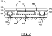
- the package 150 may be implemented as a flip chip package.
- the package 150 may implement a heat spreader/stiffener grounding scheme in accordance with the present invention.
- the package 150 may comprise a die 152 attached to a substrate 154 using, for example, flip chip solder bumps 156. A gap between the die 152 and the substrate 154 may be filled with an underfill 158.
- a stiffener 160 may be attached to the substrate 154 using an adhesive film 162 and solder (or solder balls) 164.
- the solder 164 may form a mechanical and electrical connection with grounding pads 166 on the substrate 154.
- the solder 164 may be configured to attach the stiffener 160 to the pads 166 of the substrate 154 (e.g., illustrated by solder ball 164a).
- a heat spreader 168 may be attached to (i) the die 152 using a thermally conductive material 170 and (ii) the stiffener 160 using an electrically conductive material 172.
- the solder 164 may be configured to electrically connect both the stiffener 160 and the heat spreader 168 to the pads 166 on the substrate 154 (e.g., illustrated by solder ball 164b).
- the thermally conductive material 170 may comprise a low modulus material such as thermal grease. However, other thermally conductive materials may be implemented accordingly to meet the design criteria of a particular implementation.
- the electrically conductive material 172 may comprise, in one example, a high modulus material such as electrically conductive epoxy, epoxy film, etc.
- a top (or back) side of the die 152 may be grounded using an electrically conductive material for the material 170.
- the substrate 154 may have, in one example, solder balls 174 on the side opposite the die 152.
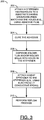
- the process 200 may comprise a step (or process) 202, a step (or process) 204, a step (or process) 206, a step (or process) 208, and a step (or process) 210.
- the step 202 generally comprises attaching a stiffener to a substrate using, in one example, an adhesive film.
- the stiffener and the adhesive film may have holes corresponding to grounding pads on the substrate.
- the step 204 generally comprises curing the adhesive film.
- the step 206 generally comprises dispensing one or more of solder, flux and/or a solder ball into the holes in the stiffener.
- the step 208 generally comprises attaching a heat spreader to the stiffener using, in one example, electrically conductive epoxy.
- the step 210 generally comprises a reflow process during which the solder (or solder balls) in the holes of the stiffener forms a solid solder-pad and solder-stiffener (or solder-stiffener-heat spreader) interface.
- a die and capacitors may be attached to the substrate using conventional techniques prior to the attachment of the stiffener.
Landscapes
- Engineering & Computer Science (AREA)
- Physics & Mathematics (AREA)
- Power Engineering (AREA)
- General Physics & Mathematics (AREA)
- Computer Hardware Design (AREA)
- Microelectronics & Electronic Packaging (AREA)
- Condensed Matter Physics & Semiconductors (AREA)
- Chemical & Material Sciences (AREA)
- Materials Engineering (AREA)
- Health & Medical Sciences (AREA)
- Electromagnetism (AREA)
- Toxicology (AREA)
- Cooling Or The Like Of Semiconductors Or Solid State Devices (AREA)
- Wire Bonding (AREA)
Applications Claiming Priority (2)
| Application Number | Priority Date | Filing Date | Title |
|---|---|---|---|
| US12/038,911 US7968999B2 (en) | 2008-02-28 | 2008-02-28 | Process of grounding heat spreader/stiffener to a flip chip package using solder and film adhesive |
| PCT/US2008/012957 WO2009108171A1 (en) | 2008-02-28 | 2008-11-20 | Process of grounding heat spreader/stiffener to a flip chip package using solder and film adhesive |
Publications (3)
| Publication Number | Publication Date |
|---|---|
| EP2248165A1 EP2248165A1 (en) | 2010-11-10 |
| EP2248165A4 EP2248165A4 (en) | 2012-04-18 |
| EP2248165B1 true EP2248165B1 (en) | 2017-01-18 |
Family
ID=41012540
Family Applications (1)
| Application Number | Title | Priority Date | Filing Date |
|---|---|---|---|
| EP08872772.2A Active EP2248165B1 (en) | 2008-02-28 | 2008-11-20 | Process of grounding heat spreader/stiffener to a flip chip package using solder and film adhesive |
Country Status (7)
| Country | Link |
|---|---|
| US (1) | US7968999B2 (enExample) |
| EP (1) | EP2248165B1 (enExample) |
| JP (1) | JP5226087B2 (enExample) |
| KR (1) | KR101177039B1 (enExample) |
| CN (1) | CN101960586B (enExample) |
| TW (1) | TWI379364B (enExample) |
| WO (1) | WO2009108171A1 (enExample) |
Families Citing this family (21)
| Publication number | Priority date | Publication date | Assignee | Title |
|---|---|---|---|---|
| US20090321925A1 (en) * | 2008-06-30 | 2009-12-31 | Gealer Charles A | Injection molded metal ic package stiffener and package-to-package interconnect frame |
| US8247900B2 (en) * | 2009-12-29 | 2012-08-21 | Taiwan Semiconductor Manufacturing Company, Ltd. | Flip chip package having enhanced thermal and mechanical performance |
| US9254532B2 (en) | 2009-12-30 | 2016-02-09 | Intel Corporation | Methods of fabricating low melting point solder reinforced sealant and structures formed thereby |
| US20110292612A1 (en) * | 2010-05-26 | 2011-12-01 | Lsi Corporation | Electronic device having electrically grounded heat sink and method of manufacturing the same |
| US8823407B2 (en) | 2012-03-01 | 2014-09-02 | Integrated Device Technology, Inc. | Test assembly for verifying heat spreader grounding in a production test |
| US9041192B2 (en) * | 2012-08-29 | 2015-05-26 | Broadcom Corporation | Hybrid thermal interface material for IC packages with integrated heat spreader |
| US8946871B2 (en) | 2012-11-07 | 2015-02-03 | Lsi Corporation | Thermal improvement of integrated circuit packages |
| US9607951B2 (en) | 2013-08-05 | 2017-03-28 | Mediatek Singapore Pte. Ltd. | Chip package |
| US9282649B2 (en) * | 2013-10-08 | 2016-03-08 | Cisco Technology, Inc. | Stand-off block |
| US9735043B2 (en) | 2013-12-20 | 2017-08-15 | Taiwan Semiconductor Manufacturing Company, Ltd. | Semiconductor packaging structure and process |
| CN105514080B (zh) * | 2014-10-11 | 2018-12-04 | 意法半导体有限公司 | 具有再分布层和加强件的电子器件及相关方法 |
| US9460980B2 (en) * | 2015-02-18 | 2016-10-04 | Qualcomm Incorporated | Systems, apparatus, and methods for heat dissipation |
| JP6569375B2 (ja) * | 2015-08-11 | 2019-09-04 | 株式会社ソシオネクスト | 半導体装置、半導体装置の製造方法及び電子装置 |
| US20170053858A1 (en) * | 2015-08-20 | 2017-02-23 | Intel Corporation | Substrate on substrate package |
| US20170170087A1 (en) | 2015-12-14 | 2017-06-15 | Intel Corporation | Electronic package that includes multiple supports |
| US20170287799A1 (en) * | 2016-04-01 | 2017-10-05 | Steven A. Klein | Removable ic package stiffener |
| CN107708328A (zh) * | 2017-06-27 | 2018-02-16 | 安徽华东光电技术研究所 | 提高芯片充分接地和散热的焊接方法 |
| JP6579396B2 (ja) * | 2017-07-18 | 2019-09-25 | 株式会社ダイレクト・アール・エフ | 半導体装置、及び基板 |
| US20190206839A1 (en) * | 2017-12-29 | 2019-07-04 | Intel Corporation | Electronic device package |
| US11081450B2 (en) * | 2019-09-27 | 2021-08-03 | Intel Corporation | Radiation shield around a component on a substrate |
| CN115116860B (zh) * | 2022-06-17 | 2025-10-28 | 北京比特大陆科技有限公司 | 芯片封装方法及芯片 |
Family Cites Families (19)
| Publication number | Priority date | Publication date | Assignee | Title |
|---|---|---|---|---|
| US5736074A (en) * | 1995-06-30 | 1998-04-07 | Micro Fab Technologies, Inc. | Manufacture of coated spheres |
| JP3437369B2 (ja) | 1996-03-19 | 2003-08-18 | 松下電器産業株式会社 | チップキャリアおよびこれを用いた半導体装置 |
| JP2770820B2 (ja) * | 1996-07-01 | 1998-07-02 | 日本電気株式会社 | 半導体装置の実装構造 |
| US6051888A (en) * | 1997-04-07 | 2000-04-18 | Texas Instruments Incorporated | Semiconductor package and method for increased thermal dissipation of flip-chip semiconductor package |
| US6011304A (en) * | 1997-05-05 | 2000-01-04 | Lsi Logic Corporation | Stiffener ring attachment with holes and removable snap-in heat sink or heat spreader/lid |
| US6114761A (en) | 1998-01-20 | 2000-09-05 | Lsi Logic Corporation | Thermally-enhanced flip chip IC package with extruded heatspreader |
| JP2000114413A (ja) * | 1998-09-29 | 2000-04-21 | Sony Corp | 半導体装置、その製造方法および部品の実装方法 |
| US6985363B2 (en) * | 2000-10-02 | 2006-01-10 | Matsushita Electric Industrial Co., Ltd. | Card type recording medium and production method therefor |
| US6639321B1 (en) | 2000-10-06 | 2003-10-28 | Lsi Logic Corporation | Balanced coefficient of thermal expansion for flip chip ball grid array |
| US6407334B1 (en) * | 2000-11-30 | 2002-06-18 | International Business Machines Corporation | I/C chip assembly |
| US6528892B2 (en) | 2001-06-05 | 2003-03-04 | International Business Machines Corporation | Land grid array stiffener use with flexible chip carriers |
| KR100394809B1 (ko) | 2001-08-09 | 2003-08-14 | 삼성전자주식회사 | 반도체 패키지 및 그 제조 방법 |
| US6472762B1 (en) | 2001-08-31 | 2002-10-29 | Lsi Logic Corporation | Enhanced laminate flipchip package using a high CTE heatspreader |
| US6854633B1 (en) * | 2002-02-05 | 2005-02-15 | Micron Technology, Inc. | System with polymer masking flux for fabricating external contacts on semiconductor components |
| US6987032B1 (en) * | 2002-07-19 | 2006-01-17 | Asat Ltd. | Ball grid array package and process for manufacturing same |
| JP4639600B2 (ja) * | 2004-02-04 | 2011-02-23 | 凸版印刷株式会社 | 半導体パッケージ |
| JP2006013029A (ja) * | 2004-06-24 | 2006-01-12 | Toppan Printing Co Ltd | 半導体パッケージ |
| US7451432B2 (en) * | 2004-10-01 | 2008-11-11 | Microsoft Corporation | Transformation of componentized and extensible workflow to a declarative format |
| JP4860994B2 (ja) * | 2005-12-06 | 2012-01-25 | ルネサスエレクトロニクス株式会社 | 半導体装置 |
-
2008
- 2008-02-28 US US12/038,911 patent/US7968999B2/en active Active
- 2008-11-10 TW TW097143311A patent/TWI379364B/zh not_active IP Right Cessation
- 2008-11-20 CN CN2008801275042A patent/CN101960586B/zh active Active
- 2008-11-20 JP JP2010548652A patent/JP5226087B2/ja not_active Expired - Fee Related
- 2008-11-20 KR KR1020107018929A patent/KR101177039B1/ko active Active
- 2008-11-20 WO PCT/US2008/012957 patent/WO2009108171A1/en not_active Ceased
- 2008-11-20 EP EP08872772.2A patent/EP2248165B1/en active Active
Non-Patent Citations (1)
| Title |
|---|
| None * |
Also Published As
| Publication number | Publication date |
|---|---|
| TWI379364B (en) | 2012-12-11 |
| JP2011513970A (ja) | 2011-04-28 |
| CN101960586B (zh) | 2012-07-18 |
| KR101177039B1 (ko) | 2012-08-27 |
| KR20100126708A (ko) | 2010-12-02 |
| EP2248165A4 (en) | 2012-04-18 |
| WO2009108171A1 (en) | 2009-09-03 |
| TW200937539A (en) | 2009-09-01 |
| US20090218680A1 (en) | 2009-09-03 |
| US7968999B2 (en) | 2011-06-28 |
| CN101960586A (zh) | 2011-01-26 |
| JP5226087B2 (ja) | 2013-07-03 |
| EP2248165A1 (en) | 2010-11-10 |
Similar Documents
| Publication | Publication Date | Title |
|---|---|---|
| EP2248165B1 (en) | Process of grounding heat spreader/stiffener to a flip chip package using solder and film adhesive | |
| KR100734816B1 (ko) | 전자 소자 캐리어를 위한 최적화된 덮개의 장착 | |
| US7426117B2 (en) | Chip on a board | |
| KR100442695B1 (ko) | 열 방출판이 부착된 플립칩 패키지 제조 방법 | |
| US20090035895A1 (en) | Chip package and chip packaging process thereof | |
| WO1998028954A2 (en) | Semiconductor packages interconnectably mounted on underlying substrates and methods of producing same | |
| CA2409912C (en) | Improvements in grounding and thermal dissipation for integrated circuit packages | |
| CA2402082A1 (en) | Method of forming an integrated circuit package at a wafer level | |
| JPH08255965A (ja) | マイクロチップモジュール組立体 | |
| JP2011040606A (ja) | 半導体装置の製造方法 | |
| TWI864404B (zh) | 雙側部分模製的系統級封裝模組 | |
| EP2023387A1 (en) | Semiconductor device, electronic parts module, and method for manufacturing the semiconductor device | |
| US20010046120A1 (en) | Chip scale packaging on cte matched printed wiring boards | |
| KR20070076084A (ko) | 스택 패키지와 그 제조 방법 | |
| US20020196615A1 (en) | Shielded electronics package structure with enhanced mechanical reliability | |
| US20060267217A1 (en) | Apparatuses and associated methods for improved solder joint reliability | |
| US20060273467A1 (en) | Flip chip package and method of conducting heat therefrom | |
| US20070235871A1 (en) | High frequency IC package and method for fabricating the same | |
| CN221102064U (zh) | 封装结构 | |
| WO2012001644A1 (en) | Method for encapsulating integrated circuit component solder joints with epoxy flux and apparatus provided with encapsulated solder joint | |
| KR100370116B1 (ko) | 반도체 패키지 및 그 제조방법 | |
| JP4112872B2 (ja) | Pgaパッケージのピン表面実装方法 | |
| JPH08236911A (ja) | ボール状外部接続端子の構造 | |
| JP2004119882A (ja) | 半導体装置 | |
| KR100666990B1 (ko) | Bga 패키지 및 그 제조방법 |
Legal Events
| Date | Code | Title | Description |
|---|---|---|---|
| PUAI | Public reference made under article 153(3) epc to a published international application that has entered the european phase |
Free format text: ORIGINAL CODE: 0009012 |
|
| 17P | Request for examination filed |
Effective date: 20100820 |
|
| AK | Designated contracting states |
Kind code of ref document: A1 Designated state(s): AT BE BG CH CY CZ DE DK EE ES FI FR GB GR HR HU IE IS IT LI LT LU LV MC MT NL NO PL PT RO SE SI SK TR |
|
| AX | Request for extension of the european patent |
Extension state: AL BA MK RS |
|
| DAX | Request for extension of the european patent (deleted) | ||
| RIC1 | Information provided on ipc code assigned before grant |
Ipc: H01L 23/10 20060101ALI20120305BHEP Ipc: H01L 23/50 20060101ALI20120305BHEP Ipc: H01L 23/498 20060101ALI20120305BHEP Ipc: H01L 23/02 20060101AFI20120305BHEP Ipc: H01L 23/552 20060101ALI20120305BHEP |
|
| A4 | Supplementary search report drawn up and despatched |
Effective date: 20120319 |
|
| 17Q | First examination report despatched |
Effective date: 20121203 |
|
| GRAP | Despatch of communication of intention to grant a patent |
Free format text: ORIGINAL CODE: EPIDOSNIGR1 |
|
| INTG | Intention to grant announced |
Effective date: 20160825 |
|
| GRAS | Grant fee paid |
Free format text: ORIGINAL CODE: EPIDOSNIGR3 |
|
| GRAA | (expected) grant |
Free format text: ORIGINAL CODE: 0009210 |
|
| AK | Designated contracting states |
Kind code of ref document: B1 Designated state(s): AT BE BG CH CY CZ DE DK EE ES FI FR GB GR HR HU IE IS IT LI LT LU LV MC MT NL NO PL PT RO SE SI SK TR |
|
| REG | Reference to a national code |
Ref country code: GB Ref legal event code: FG4D |
|
| REG | Reference to a national code |
Ref country code: CH Ref legal event code: EP |
|
| REG | Reference to a national code |
Ref country code: AT Ref legal event code: REF Ref document number: 863346 Country of ref document: AT Kind code of ref document: T Effective date: 20170215 |
|
| REG | Reference to a national code |
Ref country code: IE Ref legal event code: FG4D |
|
| REG | Reference to a national code |
Ref country code: DE Ref legal event code: R096 Ref document number: 602008048512 Country of ref document: DE |
|
| REG | Reference to a national code |
Ref country code: NL Ref legal event code: MP Effective date: 20170118 |
|
| REG | Reference to a national code |
Ref country code: LT Ref legal event code: MG4D |
|
| REG | Reference to a national code |
Ref country code: AT Ref legal event code: MK05 Ref document number: 863346 Country of ref document: AT Kind code of ref document: T Effective date: 20170118 |
|
| PG25 | Lapsed in a contracting state [announced via postgrant information from national office to epo] |
Ref country code: NL Free format text: LAPSE BECAUSE OF FAILURE TO SUBMIT A TRANSLATION OF THE DESCRIPTION OR TO PAY THE FEE WITHIN THE PRESCRIBED TIME-LIMIT Effective date: 20170118 |
|
| PG25 | Lapsed in a contracting state [announced via postgrant information from national office to epo] |
Ref country code: LT Free format text: LAPSE BECAUSE OF FAILURE TO SUBMIT A TRANSLATION OF THE DESCRIPTION OR TO PAY THE FEE WITHIN THE PRESCRIBED TIME-LIMIT Effective date: 20170118 Ref country code: FI Free format text: LAPSE BECAUSE OF FAILURE TO SUBMIT A TRANSLATION OF THE DESCRIPTION OR TO PAY THE FEE WITHIN THE PRESCRIBED TIME-LIMIT Effective date: 20170118 Ref country code: NO Free format text: LAPSE BECAUSE OF FAILURE TO SUBMIT A TRANSLATION OF THE DESCRIPTION OR TO PAY THE FEE WITHIN THE PRESCRIBED TIME-LIMIT Effective date: 20170418 Ref country code: IS Free format text: LAPSE BECAUSE OF FAILURE TO SUBMIT A TRANSLATION OF THE DESCRIPTION OR TO PAY THE FEE WITHIN THE PRESCRIBED TIME-LIMIT Effective date: 20170518 Ref country code: HR Free format text: LAPSE BECAUSE OF FAILURE TO SUBMIT A TRANSLATION OF THE DESCRIPTION OR TO PAY THE FEE WITHIN THE PRESCRIBED TIME-LIMIT Effective date: 20170118 Ref country code: GR Free format text: LAPSE BECAUSE OF FAILURE TO SUBMIT A TRANSLATION OF THE DESCRIPTION OR TO PAY THE FEE WITHIN THE PRESCRIBED TIME-LIMIT Effective date: 20170419 |
|
| PG25 | Lapsed in a contracting state [announced via postgrant information from national office to epo] |
Ref country code: PT Free format text: LAPSE BECAUSE OF FAILURE TO SUBMIT A TRANSLATION OF THE DESCRIPTION OR TO PAY THE FEE WITHIN THE PRESCRIBED TIME-LIMIT Effective date: 20170518 Ref country code: AT Free format text: LAPSE BECAUSE OF FAILURE TO SUBMIT A TRANSLATION OF THE DESCRIPTION OR TO PAY THE FEE WITHIN THE PRESCRIBED TIME-LIMIT Effective date: 20170118 Ref country code: SE Free format text: LAPSE BECAUSE OF FAILURE TO SUBMIT A TRANSLATION OF THE DESCRIPTION OR TO PAY THE FEE WITHIN THE PRESCRIBED TIME-LIMIT Effective date: 20170118 Ref country code: ES Free format text: LAPSE BECAUSE OF FAILURE TO SUBMIT A TRANSLATION OF THE DESCRIPTION OR TO PAY THE FEE WITHIN THE PRESCRIBED TIME-LIMIT Effective date: 20170118 Ref country code: LV Free format text: LAPSE BECAUSE OF FAILURE TO SUBMIT A TRANSLATION OF THE DESCRIPTION OR TO PAY THE FEE WITHIN THE PRESCRIBED TIME-LIMIT Effective date: 20170118 Ref country code: PL Free format text: LAPSE BECAUSE OF FAILURE TO SUBMIT A TRANSLATION OF THE DESCRIPTION OR TO PAY THE FEE WITHIN THE PRESCRIBED TIME-LIMIT Effective date: 20170118 Ref country code: BG Free format text: LAPSE BECAUSE OF FAILURE TO SUBMIT A TRANSLATION OF THE DESCRIPTION OR TO PAY THE FEE WITHIN THE PRESCRIBED TIME-LIMIT Effective date: 20170418 |
|
| REG | Reference to a national code |
Ref country code: DE Ref legal event code: R097 Ref document number: 602008048512 Country of ref document: DE |
|
| PG25 | Lapsed in a contracting state [announced via postgrant information from national office to epo] |
Ref country code: IT Free format text: LAPSE BECAUSE OF FAILURE TO SUBMIT A TRANSLATION OF THE DESCRIPTION OR TO PAY THE FEE WITHIN THE PRESCRIBED TIME-LIMIT Effective date: 20170118 Ref country code: RO Free format text: LAPSE BECAUSE OF FAILURE TO SUBMIT A TRANSLATION OF THE DESCRIPTION OR TO PAY THE FEE WITHIN THE PRESCRIBED TIME-LIMIT Effective date: 20170118 Ref country code: EE Free format text: LAPSE BECAUSE OF FAILURE TO SUBMIT A TRANSLATION OF THE DESCRIPTION OR TO PAY THE FEE WITHIN THE PRESCRIBED TIME-LIMIT Effective date: 20170118 Ref country code: CZ Free format text: LAPSE BECAUSE OF FAILURE TO SUBMIT A TRANSLATION OF THE DESCRIPTION OR TO PAY THE FEE WITHIN THE PRESCRIBED TIME-LIMIT Effective date: 20170118 Ref country code: SK Free format text: LAPSE BECAUSE OF FAILURE TO SUBMIT A TRANSLATION OF THE DESCRIPTION OR TO PAY THE FEE WITHIN THE PRESCRIBED TIME-LIMIT Effective date: 20170118 |
|
| PLBE | No opposition filed within time limit |
Free format text: ORIGINAL CODE: 0009261 |
|
| STAA | Information on the status of an ep patent application or granted ep patent |
Free format text: STATUS: NO OPPOSITION FILED WITHIN TIME LIMIT |
|
| PG25 | Lapsed in a contracting state [announced via postgrant information from national office to epo] |
Ref country code: DK Free format text: LAPSE BECAUSE OF FAILURE TO SUBMIT A TRANSLATION OF THE DESCRIPTION OR TO PAY THE FEE WITHIN THE PRESCRIBED TIME-LIMIT Effective date: 20170118 |
|
| 26N | No opposition filed |
Effective date: 20171019 |
|
| PG25 | Lapsed in a contracting state [announced via postgrant information from national office to epo] |
Ref country code: SI Free format text: LAPSE BECAUSE OF FAILURE TO SUBMIT A TRANSLATION OF THE DESCRIPTION OR TO PAY THE FEE WITHIN THE PRESCRIBED TIME-LIMIT Effective date: 20170118 |
|
| REG | Reference to a national code |
Ref country code: FR Ref legal event code: PLFP Year of fee payment: 10 |
|
| PG25 | Lapsed in a contracting state [announced via postgrant information from national office to epo] |
Ref country code: MC Free format text: LAPSE BECAUSE OF FAILURE TO SUBMIT A TRANSLATION OF THE DESCRIPTION OR TO PAY THE FEE WITHIN THE PRESCRIBED TIME-LIMIT Effective date: 20170118 |
|
| GBPC | Gb: european patent ceased through non-payment of renewal fee |
Effective date: 20171120 |
|
| PG25 | Lapsed in a contracting state [announced via postgrant information from national office to epo] |
Ref country code: LI Free format text: LAPSE BECAUSE OF NON-PAYMENT OF DUE FEES Effective date: 20171130 Ref country code: CH Free format text: LAPSE BECAUSE OF NON-PAYMENT OF DUE FEES Effective date: 20171130 |
|
| PG25 | Lapsed in a contracting state [announced via postgrant information from national office to epo] |
Ref country code: LU Free format text: LAPSE BECAUSE OF NON-PAYMENT OF DUE FEES Effective date: 20171120 |
|
| REG | Reference to a national code |
Ref country code: BE Ref legal event code: MM Effective date: 20171130 |
|
| REG | Reference to a national code |
Ref country code: IE Ref legal event code: MM4A |
|
| PG25 | Lapsed in a contracting state [announced via postgrant information from national office to epo] |
Ref country code: MT Free format text: LAPSE BECAUSE OF NON-PAYMENT OF DUE FEES Effective date: 20171120 |
|
| REG | Reference to a national code |
Ref country code: FR Ref legal event code: PLFP Year of fee payment: 11 |
|
| PG25 | Lapsed in a contracting state [announced via postgrant information from national office to epo] |
Ref country code: IE Free format text: LAPSE BECAUSE OF NON-PAYMENT OF DUE FEES Effective date: 20171120 |
|
| PG25 | Lapsed in a contracting state [announced via postgrant information from national office to epo] |
Ref country code: GB Free format text: LAPSE BECAUSE OF NON-PAYMENT OF DUE FEES Effective date: 20171120 Ref country code: BE Free format text: LAPSE BECAUSE OF NON-PAYMENT OF DUE FEES Effective date: 20171130 |
|
| PG25 | Lapsed in a contracting state [announced via postgrant information from national office to epo] |
Ref country code: HU Free format text: LAPSE BECAUSE OF FAILURE TO SUBMIT A TRANSLATION OF THE DESCRIPTION OR TO PAY THE FEE WITHIN THE PRESCRIBED TIME-LIMIT; INVALID AB INITIO Effective date: 20081120 |
|
| PG25 | Lapsed in a contracting state [announced via postgrant information from national office to epo] |
Ref country code: CY Free format text: LAPSE BECAUSE OF NON-PAYMENT OF DUE FEES Effective date: 20170118 |
|
| PG25 | Lapsed in a contracting state [announced via postgrant information from national office to epo] |
Ref country code: TR Free format text: LAPSE BECAUSE OF FAILURE TO SUBMIT A TRANSLATION OF THE DESCRIPTION OR TO PAY THE FEE WITHIN THE PRESCRIBED TIME-LIMIT Effective date: 20170118 |
|
| P01 | Opt-out of the competence of the unified patent court (upc) registered |
Effective date: 20230521 |
|
| PGFP | Annual fee paid to national office [announced via postgrant information from national office to epo] |
Ref country code: DE Payment date: 20241022 Year of fee payment: 17 |
|
| PGFP | Annual fee paid to national office [announced via postgrant information from national office to epo] |
Ref country code: FR Payment date: 20241022 Year of fee payment: 17 |
|
| REG | Reference to a national code |
Ref country code: DE Ref legal event code: R079 Ref document number: 602008048512 Country of ref document: DE Free format text: PREVIOUS MAIN CLASS: H01L0023020000 Ipc: H10W0076100000 |