EP2221875B1 - Multi finger MOS transistor - Google Patents
Multi finger MOS transistor Download PDFInfo
- Publication number
- EP2221875B1 EP2221875B1 EP10154307A EP10154307A EP2221875B1 EP 2221875 B1 EP2221875 B1 EP 2221875B1 EP 10154307 A EP10154307 A EP 10154307A EP 10154307 A EP10154307 A EP 10154307A EP 2221875 B1 EP2221875 B1 EP 2221875B1
- Authority
- EP
- European Patent Office
- Prior art keywords
- source regions
- holes
- metal
- ground potential
- supply line
- Prior art date
- Legal status (The legal status is an assumption and is not a legal conclusion. Google has not performed a legal analysis and makes no representation as to the accuracy of the status listed.)
- Not-in-force
Links
- 239000002184 metal Substances 0.000 claims description 67
- 239000004065 semiconductor Substances 0.000 claims description 42
- 229910044991 metal oxide Inorganic materials 0.000 claims description 14
- 150000004706 metal oxides Chemical class 0.000 claims description 14
- 239000003870 refractory metal Substances 0.000 claims description 8
- 239000012141 concentrate Substances 0.000 claims description 2
- 238000000034 method Methods 0.000 description 6
- 230000015556 catabolic process Effects 0.000 description 4
- 230000006378 damage Effects 0.000 description 3
- 239000000463 material Substances 0.000 description 3
- 230000005611 electricity Effects 0.000 description 2
- 238000011156 evaluation Methods 0.000 description 2
- 238000002474 experimental method Methods 0.000 description 2
- 230000003068 static effect Effects 0.000 description 2
- 238000012360 testing method Methods 0.000 description 2
- VYPSYNLAJGMNEJ-UHFFFAOYSA-N Silicium dioxide Chemical compound O=[Si]=O VYPSYNLAJGMNEJ-UHFFFAOYSA-N 0.000 description 1
- 238000010586 diagram Methods 0.000 description 1
- 230000000694 effects Effects 0.000 description 1
- 230000001747 exhibiting effect Effects 0.000 description 1
- 230000036039 immunity Effects 0.000 description 1
- 239000012535 impurity Substances 0.000 description 1
- 238000004519 manufacturing process Methods 0.000 description 1
- 239000007769 metal material Substances 0.000 description 1
- 238000012986 modification Methods 0.000 description 1
- 230000004048 modification Effects 0.000 description 1
- 229910021420 polycrystalline silicon Inorganic materials 0.000 description 1
- 229920005591 polysilicon Polymers 0.000 description 1
- 229910052814 silicon oxide Inorganic materials 0.000 description 1
- 239000000758 substrate Substances 0.000 description 1
Images


Classifications
-
- H—ELECTRICITY
- H01—ELECTRIC ELEMENTS
- H01L—SEMICONDUCTOR DEVICES NOT COVERED BY CLASS H10
- H01L29/00—Semiconductor devices specially adapted for rectifying, amplifying, oscillating or switching and having potential barriers; Capacitors or resistors having potential barriers, e.g. a PN-junction depletion layer or carrier concentration layer; Details of semiconductor bodies or of electrodes thereof ; Multistep manufacturing processes therefor
- H01L29/40—Electrodes ; Multistep manufacturing processes therefor
- H01L29/41—Electrodes ; Multistep manufacturing processes therefor characterised by their shape, relative sizes or dispositions
- H01L29/417—Electrodes ; Multistep manufacturing processes therefor characterised by their shape, relative sizes or dispositions carrying the current to be rectified, amplified or switched
- H01L29/41725—Source or drain electrodes for field effect devices
- H01L29/41758—Source or drain electrodes for field effect devices for lateral devices with structured layout for source or drain region, i.e. the source or drain region having cellular, interdigitated or ring structure or being curved or angular
-
- H—ELECTRICITY
- H01—ELECTRIC ELEMENTS
- H01L—SEMICONDUCTOR DEVICES NOT COVERED BY CLASS H10
- H01L21/00—Processes or apparatus adapted for the manufacture or treatment of semiconductor or solid state devices or of parts thereof
- H01L21/02—Manufacture or treatment of semiconductor devices or of parts thereof
- H01L21/02041—Cleaning
- H01L21/02057—Cleaning during device manufacture
- H01L21/0206—Cleaning during device manufacture during, before or after processing of insulating layers
- H01L21/02063—Cleaning during device manufacture during, before or after processing of insulating layers the processing being the formation of vias or contact holes
-
- H—ELECTRICITY
- H01—ELECTRIC ELEMENTS
- H01L—SEMICONDUCTOR DEVICES NOT COVERED BY CLASS H10
- H01L27/00—Devices consisting of a plurality of semiconductor or other solid-state components formed in or on a common substrate
- H01L27/02—Devices consisting of a plurality of semiconductor or other solid-state components formed in or on a common substrate including semiconductor components specially adapted for rectifying, oscillating, amplifying or switching and having potential barriers; including integrated passive circuit elements having potential barriers
- H01L27/0203—Particular design considerations for integrated circuits
- H01L27/0248—Particular design considerations for integrated circuits for electrical or thermal protection, e.g. electrostatic discharge [ESD] protection
- H01L27/0251—Particular design considerations for integrated circuits for electrical or thermal protection, e.g. electrostatic discharge [ESD] protection for MOS devices
- H01L27/0266—Particular design considerations for integrated circuits for electrical or thermal protection, e.g. electrostatic discharge [ESD] protection for MOS devices using field effect transistors as protective elements
-
- H—ELECTRICITY
- H01—ELECTRIC ELEMENTS
- H01L—SEMICONDUCTOR DEVICES NOT COVERED BY CLASS H10
- H01L29/00—Semiconductor devices specially adapted for rectifying, amplifying, oscillating or switching and having potential barriers; Capacitors or resistors having potential barriers, e.g. a PN-junction depletion layer or carrier concentration layer; Details of semiconductor bodies or of electrodes thereof ; Multistep manufacturing processes therefor
- H01L29/40—Electrodes ; Multistep manufacturing processes therefor
- H01L29/43—Electrodes ; Multistep manufacturing processes therefor characterised by the materials of which they are formed
- H01L29/49—Metal-insulator-semiconductor electrodes, e.g. gates of MOSFET
-
- H—ELECTRICITY
- H01—ELECTRIC ELEMENTS
- H01L—SEMICONDUCTOR DEVICES NOT COVERED BY CLASS H10
- H01L29/00—Semiconductor devices specially adapted for rectifying, amplifying, oscillating or switching and having potential barriers; Capacitors or resistors having potential barriers, e.g. a PN-junction depletion layer or carrier concentration layer; Details of semiconductor bodies or of electrodes thereof ; Multistep manufacturing processes therefor
- H01L29/66—Types of semiconductor device ; Multistep manufacturing processes therefor
- H01L29/68—Types of semiconductor device ; Multistep manufacturing processes therefor controllable by only the electric current supplied, or only the electric potential applied, to an electrode which does not carry the current to be rectified, amplified or switched
- H01L29/76—Unipolar devices, e.g. field effect transistors
- H01L29/772—Field effect transistors
- H01L29/78—Field effect transistors with field effect produced by an insulated gate
- H01L29/786—Thin film transistors, i.e. transistors with a channel being at least partly a thin film
- H01L29/78606—Thin film transistors, i.e. transistors with a channel being at least partly a thin film with supplementary region or layer in the thin film or in the insulated bulk substrate supporting it for controlling or increasing the safety of the device
- H01L29/78618—Thin film transistors, i.e. transistors with a channel being at least partly a thin film with supplementary region or layer in the thin film or in the insulated bulk substrate supporting it for controlling or increasing the safety of the device characterised by the drain or the source properties, e.g. the doping structure, the composition, the sectional shape or the contact structure
- H01L29/78621—Thin film transistors, i.e. transistors with a channel being at least partly a thin film with supplementary region or layer in the thin film or in the insulated bulk substrate supporting it for controlling or increasing the safety of the device characterised by the drain or the source properties, e.g. the doping structure, the composition, the sectional shape or the contact structure with LDD structure or an extension or an offset region or characterised by the doping profile
- H01L29/78624—Thin film transistors, i.e. transistors with a channel being at least partly a thin film with supplementary region or layer in the thin film or in the insulated bulk substrate supporting it for controlling or increasing the safety of the device characterised by the drain or the source properties, e.g. the doping structure, the composition, the sectional shape or the contact structure with LDD structure or an extension or an offset region or characterised by the doping profile the source and the drain regions being asymmetrical
-
- H—ELECTRICITY
- H01—ELECTRIC ELEMENTS
- H01L—SEMICONDUCTOR DEVICES NOT COVERED BY CLASS H10
- H01L2924/00—Indexing scheme for arrangements or methods for connecting or disconnecting semiconductor or solid-state bodies as covered by H01L24/00
- H01L2924/10—Details of semiconductor or other solid state devices to be connected
- H01L2924/11—Device type
- H01L2924/13—Discrete devices, e.g. 3 terminal devices
- H01L2924/1304—Transistor
- H01L2924/1306—Field-effect transistor [FET]
- H01L2924/13091—Metal-Oxide-Semiconductor Field-Effect Transistor [MOSFET]
Definitions
- the present invention relates to a semiconductor device including a multi-finger type metal oxide semiconductor (MOS) transistor.
- MOS metal oxide semiconductor
- the present invention relates to a semiconductor device using an n-type MOS (NMOS) transistor as an electrostatic discharge (hereinafter, referred to as ESD) protection element.
- NMOS n-type MOS
- ESD electrostatic discharge
- an off transistor which is an NMOS transistor provided in an off-state whose gate potential is fixed to a ground (Vss), is used as an ESD protection element for preventing breakdown of an internal circuit due to static electricity supplied from a pad provided for external connection.
- the off transistor Since the off transistor must allow a large amount of current generated by static electricity to flow at once unlike ordinary MOS transistors forming an internal circuit such as a logic circuit, the off transistor is formed to have a large width (width W) of about several hundred micrometers in many cases.
- the off transistor often takes a form of multi-finger which is obtained by combining a plurality of drain regions, source regions, and gate electrodes into a comb shape.
- the combinatorial structure of a plurality of transistors causes a difficulty in uniformly operating the whole NMOS transistors for ESD protection. For example, current concentration occurs in a portion closer to the external connection terminal, resulting in the breakdown of the off transistor without sufficiently exhibiting the original ESD protection function.
- a distance between a contact hole formed on a drain region and a gate electrode is made smaller as a distance from the external connection terminal becomes longer to accelerate the operation of the transistor (for example, refer to FIG. 2 of JP 7-45829 A ).
- a length of a salicide block deposed on a drain region to protect the drain region from covering by the salicide is made longer as a distance from a substrate contact becomes longer to obtain a uniform operation of the transistor (for example, refer to JP 2007-116049 A ).
- the protection function is, however, not sufficiently accomplished. Further, in the method of JP 7-45829 A , the distance between the contact and the gate electrode in the drain region is adjusted to thereby locally adjust a transistor operation speed.
- the method however, has problems that a desired contact position cannot be ensured along with a reduction in width of the drain region, that line resistance has been made low through a use of an interconnect including a refractory metal in recent years to thereby accelerate the propagation speed of a surge, causing a case where the transistor operation speed cannot be adjusted only by the distance between the contact and the gate electrode, and that it is difficult to adapt the method to a case in which interconnect to the transistor is introduced from a direction perpendicular to the width direction of the transistor.
- the patent document JP 2007-116049 A discloses a method for a local control of the operating speed of a transistor by adjusting the length of the salicide block on the drain region.
- the method has problems that a predetermined length cannot be assured due to a variation caused in a manufacturing process, that line resistance has been made low through a use of an interconnect including a refractory metal in recent years to thereby accelerate the propagation speed of a surge, causing concentration of surges into a particular region of a salicide region, and that an occupation area by the NMOS off transistor increases due to an adjustment of the length of the salicide block.
- a semiconductor device according to the present invention is provided as defined in claim 1.
- the plurality of layers of metal interconnects other than the first metal interconnect may be introduced in a direction perpendicular to a channel width direction of the n-type metal oxide semiconductor transistor for electrostatic discharge protection, the first metal interconnect may be placed in a direction parallel to the channel width direction of the n-type metal oxide semiconductor transistor for electrostatic discharge protection, and the plurality of layers of metal interconnects other than the first metal interconnect may be connected to the first metal interconnect via the via-holes on the plurality of source regions.
- the via-holes may be placed to be widely distributed in the direction parallel to the channel width direction of the n-type metal oxide semiconductor transistor for electrostatic discharge protection on the plurality of source regions.
- the via-holes may be placed to be concentrated on a part of each of the plurality of source regions.
- the number of the via-holes disposed for connecting the first metal interconnect and the plurality of layers of metal interconnects other than the first metal interconnect may be controlled to have a ratio less than four due to the distance of an interconnect connected to the n-type metal oxide semiconductor transistor from outside.
- the interconnect introduced to the n-type metal oxide semiconductor transistor for electrostatic discharge protection is introduced in the direction perpendicular to the channel width direction of the n-type metal oxide semiconductor transistor for electrostatic discharge protection using a high-speed multilayer interconnect including a refractory metal, employment of those means enables the interconnect to uniformly operate in the entire n-type metal oxide semiconductor transistor for electrostatic discharge protection.
- the semiconductor device including the n-type metal oxide semiconductor transistor for electrostatic discharge protection provided with a sufficient electrostatic discharge protection function can be obtained.
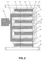
- FIG. 1 is a schematic plan view showing an NMOS transistor for ESD protection of a semiconductor device according to a first embodiment of the present invention.
- a first source region 101 and a first drain region 301 are formed of an n-type heavily-doped impurity region. Between the first source region 101 and the first drain region 301, a gate insulating film (not shown) made of a silicon oxide film or the like is formed, and a gate electrode 201 made of a polysilicon or the like are formed thereon. Arranging a mirror-reflected pattern repeatedly, there are formed a second source region 102 via the gate electrode 201 from the first drain region 301, the second drain region 302 via the gate electrode 201, and a third source region 103 via the gate electrode 201, and the third drain region 303 via the gate electrode 201, and the fourth source region 104 via the gate electrode 201.
- the first embodiment shows an example in which four source regions, three drain regions, and six gate electrodes are placed to form a comb shape. As a MOS transistor, six transistors are combined.
- a ground potential is supplied to the first source region 101, the second source region 102, the third source 103 and the fourth source region 104, by means of a second metal interconnect 711 which is formed of a material including a refractory metal and has a form of a wing and is connected to ground potential supply lines 701 which is arranged on both sides of the NMOS transistor and is formed of the metal material including the refractory metal and is formed of a wide interconnect having a low resistance.
- the second metal interconnect 711 is placed from the ground potential supply line 701 in a direction perpendicular to a channel width direction of the NMOS transistor for ESD protection, and is connected to a first metal interconnect 901 formed of the material including the refractory metal through the via-holes 601. Further, the first metal interconnect 901 is connected to the first source region 101, the second source region 102, the third source region 103 and the fourth source region 104 through contact holes though not shown for simplicity.
- the number of via-holes 601 is set largest on the second source region 102 or the third source region 103 placed farthest from the ground potential supply line 701, and set smallest on the first source region 101 or the fourth source region 104 placed closest to the ground potential supply line 701.
- each sum of an line resistance of the second metal interconnect 711 connected to the ground potential supply line 701 and a contact resistance through the via-holes 601 arranged on each of the first metal interconnects formed on each of the source regions can be made substantially equal to one another, permitting a uniform operation in the entire NMOS transistor for ESD protection without concentrating to a part close to the ground potential supply line 701.
- This embodiment shows a case where a width of the second metal interconnect 711 increases as a distance between the ground potential supply line 701 and the second metal interconnect 711 becomes larger, and with such a structure, an effect of the line resistance of the second metal interconnect 711 can be mitigated.
- a first metal interconnect 811 made of the material including the refractory metal is connected to an external connection terminal 801 at one end, and is connected to the first drain region 301, the second drain region 302, and the third drain region 303 at the other end.
- the first drain region 301, the drain region 302, and the third drain region are connected to the first metal interconnect 811 via contact holes, which are not shown in the drawing.
- the metal interconnect for supplying and fixing the potentials of the source regions of the NMOS transistor for ESD protection is set to be the second metal interconnect
- the interconnect connected to the drain regions is set to be the first metal interconnect.
- the first metal interconnect may be the line for supplying and fixing the potentials of the source regions
- the second metal interconnect may be the line connected to the drains, or a combination thereof may be provided at will.
- FIG. 1 shows an example in which two layers of metal interconnects are used, but a plurality of metal layers equal to or more than three layers may be used. In such a case, attention must be paid to the similar points as in the case of using two layers described above.
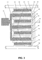
- FIG. 2 is a schematic plan view showing an NMOS transistor for ESD protection of a semiconductor device according to a second embodiment of the present invention. Counterparts corresponding to the parts of FIG. 1 are denoted by the same reference numerals.
- the second embodiment is different from the first embodiment shown in FIG. 1 in an arrangement of the via-holes 601.
- the via-holes 601 placed over the first source region 101, the second source region 102, and the third source region 103 are arranged to have a wide distribution in a direction parallel to the channel width direction of the NMOS transistor for ESD protection.
- the via-holes 601 are placed to concentrate to a part above each of the first source region 101, the second source region 102, and the third source region 103.
- the line resistance of the metal line 811 differs between a side close to and a side apart from the external connection terminal 801 in the channel width direction, making a portion of the first drain region 301, a portion of the second drain region 302, and a portion of the third drain region 303, which are closer to the external connection terminal 801, relatively easy to operate.
- the via-holes 601 are provided so as to be concentrated in regions apart from the external connection terminal 801, with the result that generation of distance dependence to the external connection terminal 801 in the channel width direction is mitigated during operation of the NMOS transistor for ESD protection.
- the second embodiment of FIG. 2 shows an example in which the line for supplying and fixing the potentials of the source regions of the NMOS transistor for ESD protection is supposed to be the second metal interconnect, and the line connected to the drain regions is supposed to be the first metal interconnect.
- the first metal interconnect may be the line for supplying and fixing the potentials of the source regions
- the second metal interconnect may be the line connected to the drain regions, or a combination thereof may be provided at will.
- the number of via-holes placed on the side where the second metal interconnect is used should be set so that, according to the gist of the description of the first embodiment shown in FIG. 1 , the sums of the line resistance and the resistance between the interconnects, in which the contact resistance of via-holes is included, introduced to the plurality of source regions of the NMOS transistor for ESD protection and the resistances among the interconnects are substantially equal, and a plurality of metal interconnects equal to or more than three layers may be used. Explanations for other parts denoted by the same reference numerals as FIG. 1 are omitted.
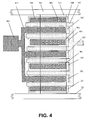
- FIG. 3 is a schematic plan view showing an NMOS transistor for ESD protection of a semiconductor device according to a third embodiment of the present invention. Since the drawing resembles to the first embodiment shown in FIG. 1 , explanations for the same points as in the first embodiment is omitted and explanations for different points from the first embodiment is given.
- the third embodiment is different from the first embodiment shown in FIG. 1 in an arrangement of the via-holes 601 to which explanation is given.
- the number of the via-holes 601 placed on the side where the second metal interconnect is used is controlled so that the sums of the line resistance and the resistance between the interconnects, in which the contact resistance of via-holes is included, introduced to the plurality of source regions of the NMOS transistor for ESD protection and the resistances among the interconnects are substantially equal, according to the gist of the description of the first embodiment shown in FIG. 1 .
- an experimental result for the upper limit of the number of via-holes having a predetermined size is shown in FIG. 5 .
- FIG. 5 shows an experimental result for an optimum number for arrangement of via-holes for improving the ESD immunity.
- FIG. 5A shows a schematic plan view of an evaluation sample structure. All the via-holes have the same size. Gate electrodes and drain regions are omitted for simplicity.
- FIG.5B shows an occurrence ratio of the number of destruction identified by photoemission after the pulses were applied to the evaluation sample until destruction occurs under an HMB mode ESD test.
- the numbers 1, 1, 2, 3, and 4 appearing along the horizontal axis are ratios for the number of via-holes at each point against the point A, to each point corresponding to the point A, point B, point C, point D, and point E, respectively. From the experiment it can be seen that frequent ESD destruction occurs at the point E where the via-hole number ratio is four times more though the distance from the ground potential supply line is the same for the point A and point E.
- the result shows that it is important to set the number of via-holes placed on the second source region 102 and the third source region 103 which are disposed farthest from the ground potential supply line 701 less than four times the number of via-holes placed on the first source region 101 and the fourth source region 104 which are disposed nearest to the ground potential supply line 701. Accordingly in a case where the number of fingers increases to extend the transistor width W, uniform operation in the whole of the NMOS transistor for ESD protection can be made by setting the number of via-holes placed on the source region which is disposed farthest from the ground potential supply line less than four times the number of via-holes placed on the source region which is disposed nearest to the ground potential supply line.
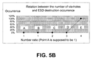
- FIG. 4 is a schematic plan view showing an NMOS transistor for ESD protection of a semiconductor device according to a fourth embodiment of the present invention.
- the second embodiment and the third embodiment are combined. Though a detailed explanation is omitted, it is seen easily that in a case where the number of fingers increases to extend the transistor width W, uniform operation in the whole of the NMOS transistor for ESD protection can be made by setting the number of via-holes placed on the source region which is disposed farthest from the ground potential supply line 701 less than four times of the number of via-holes placed on the source region which is disposed nearest to the ground potential supply line 701.
- FIG. 6 is a schematic plan view showing an NMOS transistor for ESD protection of a semiconductor device according to a fifth embodiment of the present invention. Counterparts corresponding to the parts of FIG. 1 are denoted by the same reference numerals.
- the fifth embodiment is different from the first embodiment shown in FIG. 1 in an arrangement of the linear via-holes 1101 having a constant width and a different length above each source region.
- linear via-holes 1101 instead of via-holes 601, increase in the contact area with the first metal interconnect eases realization of low resistance connection, permitting a higher propagation speed of the ESD surge for faster conduction and easier operation while holding features described in the first embodiment.
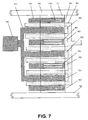
- FIG. 7 is a schematic plan view showing an NMOS transistor for ESD protection of a semiconductor device according to a sixth embodiment of the present invention. Counterparts corresponding to the parts of FIG. 2 are denoted by the same reference numerals.
- the sixth embodiment is different from the second embodiment shown in FIG. 2 in an arrangement of the linear via-holes 1101 having a constant width and a different length above the each source region.
- linear via-holes 1101 instead of via-holes 601, increase in the contact area with the first metal interconnect eases realization of low resistance connection, permitting a higher propagation speed of the ESD surge for faster conduction and easier operation while holding features described in the first embodiment.
Landscapes
- Engineering & Computer Science (AREA)
- Power Engineering (AREA)
- Microelectronics & Electronic Packaging (AREA)
- Physics & Mathematics (AREA)
- Condensed Matter Physics & Semiconductors (AREA)
- General Physics & Mathematics (AREA)
- Computer Hardware Design (AREA)
- Ceramic Engineering (AREA)
- Manufacturing & Machinery (AREA)
- Semiconductor Integrated Circuits (AREA)
- Metal-Oxide And Bipolar Metal-Oxide Semiconductor Integrated Circuits (AREA)
Applications Claiming Priority (2)
| Application Number | Priority Date | Filing Date | Title |
|---|---|---|---|
| JP2009039345 | 2009-02-23 | ||
| JP2010016340A JP5603089B2 (ja) | 2009-02-23 | 2010-01-28 | 半導体装置 |
Publications (3)
| Publication Number | Publication Date |
|---|---|
| EP2221875A2 EP2221875A2 (en) | 2010-08-25 |
| EP2221875A3 EP2221875A3 (en) | 2011-10-19 |
| EP2221875B1 true EP2221875B1 (en) | 2012-12-19 |
Family
ID=42101475
Family Applications (1)
| Application Number | Title | Priority Date | Filing Date |
|---|---|---|---|
| EP10154307A Not-in-force EP2221875B1 (en) | 2009-02-23 | 2010-02-22 | Multi finger MOS transistor |
Country Status (6)
| Country | Link |
|---|---|
| US (1) | US8373231B2 (ko) |
| EP (1) | EP2221875B1 (ko) |
| JP (1) | JP5603089B2 (ko) |
| KR (1) | KR101629968B1 (ko) |
| CN (1) | CN101814501B (ko) |
| TW (1) | TWI472014B (ko) |
Families Citing this family (19)
| Publication number | Priority date | Publication date | Assignee | Title |
|---|---|---|---|---|
| US7483001B2 (en) * | 2001-11-21 | 2009-01-27 | Seiko Epson Corporation | Active matrix substrate, electro-optical device, and electronic device |
| CN102446961B (zh) * | 2011-12-09 | 2014-05-28 | 无锡中星微电子有限公司 | 包含功率器件的半导体装置及其制备方法 |
| CN102854643B (zh) * | 2012-09-04 | 2015-11-25 | 深圳市华星光电技术有限公司 | 一种液晶显示面板及其制造方法 |
| JP6013876B2 (ja) | 2012-10-30 | 2016-10-25 | エスアイアイ・セミコンダクタ株式会社 | 半導体装置 |
| JP6033054B2 (ja) | 2012-11-22 | 2016-11-30 | エスアイアイ・セミコンダクタ株式会社 | 半導体装置 |
| JP5923046B2 (ja) * | 2013-01-11 | 2016-05-24 | 株式会社東芝 | 半導体装置の製造方法 |
| JP2014154595A (ja) * | 2013-02-05 | 2014-08-25 | Seiko Instruments Inc | 半導体装置 |
| JP6100026B2 (ja) * | 2013-03-06 | 2017-03-22 | エスアイアイ・セミコンダクタ株式会社 | 半導体装置 |
| JP2014229737A (ja) | 2013-05-22 | 2014-12-08 | 株式会社東芝 | 半導体装置 |
| TWI532191B (zh) * | 2013-12-31 | 2016-05-01 | 友達光電股份有限公司 | 薄膜電晶體結構 |
| CN107851583B (zh) | 2015-08-21 | 2021-04-02 | 日立汽车系统株式会社 | 半导体装置、半导体集成电路以及负载驱动装置 |
| CN109148555B (zh) * | 2017-06-27 | 2021-08-31 | 深圳尚阳通科技有限公司 | 超结器件及其制造方法 |
| CN109148557B (zh) * | 2017-06-27 | 2021-06-11 | 深圳尚阳通科技有限公司 | 超结器件及其制造方法 |
| CN109148558B (zh) * | 2017-06-27 | 2021-08-10 | 深圳尚阳通科技有限公司 | 超结器件及其制造方法 |
| CN109148556B (zh) * | 2017-06-27 | 2022-02-15 | 深圳尚阳通科技有限公司 | 超结器件及其制造方法 |
| CN108879634B (zh) * | 2018-06-30 | 2022-03-04 | 唯捷创芯(天津)电子技术股份有限公司 | 一种浪涌保护器件及其组成的芯片、通信终端 |
| JP2021141138A (ja) * | 2020-03-03 | 2021-09-16 | キオクシア株式会社 | 半導体装置 |
| CA3114695A1 (en) * | 2020-04-08 | 2021-10-08 | National Research Council Of Canada | Distributed inductance integrated field effect transistor structure |
| CN114664725A (zh) * | 2020-12-23 | 2022-06-24 | 华润微电子(重庆)有限公司 | GaN器件互联结构及其制备方法 |
Family Cites Families (11)
| Publication number | Priority date | Publication date | Assignee | Title |
|---|---|---|---|---|
| JPH0745829A (ja) * | 1993-07-28 | 1995-02-14 | Ricoh Co Ltd | 半導体集積回路装置 |
| JP2865132B2 (ja) * | 1996-07-19 | 1999-03-08 | 日本電気株式会社 | 半導体装置の入出力静電保護回路 |
| US6587320B1 (en) * | 2000-01-04 | 2003-07-01 | Sarnoff Corporation | Apparatus for current ballasting ESD sensitive devices |
| JP4144225B2 (ja) * | 2002-01-29 | 2008-09-03 | 株式会社デンソー | ダイオードおよびその製造方法 |
| TW578447B (en) * | 2003-04-04 | 2004-03-01 | Arima Computer Corp | An electrostatic discharge protection structure for a multi-hole structure |
| JP2004311670A (ja) * | 2003-04-07 | 2004-11-04 | Toshiba Lsi System Support Kk | 半導体装置 |
| US6927458B2 (en) * | 2003-08-08 | 2005-08-09 | Conexant Systems, Inc. | Ballasting MOSFETs using staggered and segmented diffusion regions |
| JP2006278677A (ja) * | 2005-03-29 | 2006-10-12 | Mitsumi Electric Co Ltd | 半導体装置 |
| JP2007116049A (ja) * | 2005-10-24 | 2007-05-10 | Toshiba Corp | 半導体装置 |
| JP5165967B2 (ja) * | 2007-08-22 | 2013-03-21 | セイコーインスツル株式会社 | 半導体装置 |
| CN201213133Y (zh) * | 2008-02-20 | 2009-03-25 | 和舰科技(苏州)有限公司 | 一种更均匀导通的电容耦合静电放电防护器件 |
-
2010
- 2010-01-28 JP JP2010016340A patent/JP5603089B2/ja not_active Expired - Fee Related
- 2010-02-11 TW TW99104435A patent/TWI472014B/zh not_active IP Right Cessation
- 2010-02-22 US US12/709,762 patent/US8373231B2/en active Active
- 2010-02-22 EP EP10154307A patent/EP2221875B1/en not_active Not-in-force
- 2010-02-22 KR KR1020100015648A patent/KR101629968B1/ko active IP Right Grant
- 2010-02-23 CN CN201010131740.0A patent/CN101814501B/zh not_active Expired - Fee Related
Also Published As
| Publication number | Publication date |
|---|---|
| KR20100096027A (ko) | 2010-09-01 |
| EP2221875A3 (en) | 2011-10-19 |
| KR101629968B1 (ko) | 2016-06-13 |
| JP5603089B2 (ja) | 2014-10-08 |
| CN101814501A (zh) | 2010-08-25 |
| CN101814501B (zh) | 2014-09-03 |
| TWI472014B (zh) | 2015-02-01 |
| JP2010219504A (ja) | 2010-09-30 |
| US20100213549A1 (en) | 2010-08-26 |
| EP2221875A2 (en) | 2010-08-25 |
| TW201103124A (en) | 2011-01-16 |
| US8373231B2 (en) | 2013-02-12 |
Similar Documents
| Publication | Publication Date | Title |
|---|---|---|
| EP2221875B1 (en) | Multi finger MOS transistor | |
| US7750409B2 (en) | Semiconductor device | |
| US7893497B2 (en) | Semiconductor device | |
| KR101761922B1 (ko) | 반도체 장치 | |
| US20080135940A1 (en) | Semiconductor Device | |
| US9136263B2 (en) | Semiconductor device | |
| JP5546191B2 (ja) | 半導体装置 | |
| EP2966675B1 (en) | Semiconductor device | |
| KR102082644B1 (ko) | 반도체 장치 | |
| EP2590219A1 (en) | Semiconductor device | |
| TWI575698B (zh) | 半導體裝置 |
Legal Events
| Date | Code | Title | Description |
|---|---|---|---|
| PUAI | Public reference made under article 153(3) epc to a published international application that has entered the european phase |
Free format text: ORIGINAL CODE: 0009012 |
|
| AK | Designated contracting states |
Kind code of ref document: A2 Designated state(s): AT BE BG CH CY CZ DE DK EE ES FI FR GB GR HR HU IE IS IT LI LT LU LV MC MK MT NL NO PL PT RO SE SI SK SM TR |
|
| AX | Request for extension of the european patent |
Extension state: AL BA RS |
|
| PUAL | Search report despatched |
Free format text: ORIGINAL CODE: 0009013 |
|
| AK | Designated contracting states |
Kind code of ref document: A3 Designated state(s): AT BE BG CH CY CZ DE DK EE ES FI FR GB GR HR HU IE IS IT LI LT LU LV MC MK MT NL NO PL PT RO SE SI SK SM TR |
|
| AX | Request for extension of the european patent |
Extension state: AL BA RS |
|
| RIC1 | Information provided on ipc code assigned before grant |
Ipc: H01L 27/02 20060101ALI20110913BHEP Ipc: H01L 29/417 20060101AFI20110913BHEP |
|
| 17P | Request for examination filed |
Effective date: 20120328 |
|
| RIC1 | Information provided on ipc code assigned before grant |
Ipc: H01L 27/02 20060101ALI20120531BHEP Ipc: H01L 29/417 20060101AFI20120531BHEP |
|
| GRAP | Despatch of communication of intention to grant a patent |
Free format text: ORIGINAL CODE: EPIDOSNIGR1 |
|
| GRAS | Grant fee paid |
Free format text: ORIGINAL CODE: EPIDOSNIGR3 |
|
| GRAA | (expected) grant |
Free format text: ORIGINAL CODE: 0009210 |
|
| AK | Designated contracting states |
Kind code of ref document: B1 Designated state(s): AT BE BG CH CY CZ DE DK EE ES FI FR GB GR HR HU IE IS IT LI LT LU LV MC MK MT NL NO PL PT RO SE SI SK SM TR |
|
| REG | Reference to a national code |
Ref country code: GB Ref legal event code: FG4D |
|
| REG | Reference to a national code |
Ref country code: CH Ref legal event code: EP |
|
| REG | Reference to a national code |
Ref country code: AT Ref legal event code: REF Ref document number: 589786 Country of ref document: AT Kind code of ref document: T Effective date: 20130115 |
|
| REG | Reference to a national code |
Ref country code: DE Ref legal event code: R096 Ref document number: 602010004133 Country of ref document: DE Effective date: 20130221 |
|
| PG25 | Lapsed in a contracting state [announced via postgrant information from national office to epo] |
Ref country code: LT Free format text: LAPSE BECAUSE OF FAILURE TO SUBMIT A TRANSLATION OF THE DESCRIPTION OR TO PAY THE FEE WITHIN THE PRESCRIBED TIME-LIMIT Effective date: 20121219 Ref country code: FI Free format text: LAPSE BECAUSE OF FAILURE TO SUBMIT A TRANSLATION OF THE DESCRIPTION OR TO PAY THE FEE WITHIN THE PRESCRIBED TIME-LIMIT Effective date: 20121219 Ref country code: ES Free format text: LAPSE BECAUSE OF FAILURE TO SUBMIT A TRANSLATION OF THE DESCRIPTION OR TO PAY THE FEE WITHIN THE PRESCRIBED TIME-LIMIT Effective date: 20130330 Ref country code: SE Free format text: LAPSE BECAUSE OF FAILURE TO SUBMIT A TRANSLATION OF THE DESCRIPTION OR TO PAY THE FEE WITHIN THE PRESCRIBED TIME-LIMIT Effective date: 20121219 Ref country code: NO Free format text: LAPSE BECAUSE OF FAILURE TO SUBMIT A TRANSLATION OF THE DESCRIPTION OR TO PAY THE FEE WITHIN THE PRESCRIBED TIME-LIMIT Effective date: 20130319 |
|
| REG | Reference to a national code |
Ref country code: NL Ref legal event code: VDEP Effective date: 20121219 Ref country code: AT Ref legal event code: MK05 Ref document number: 589786 Country of ref document: AT Kind code of ref document: T Effective date: 20121219 |
|
| REG | Reference to a national code |
Ref country code: LT Ref legal event code: MG4D |
|
| PG25 | Lapsed in a contracting state [announced via postgrant information from national office to epo] |
Ref country code: SI Free format text: LAPSE BECAUSE OF FAILURE TO SUBMIT A TRANSLATION OF THE DESCRIPTION OR TO PAY THE FEE WITHIN THE PRESCRIBED TIME-LIMIT Effective date: 20121219 Ref country code: LV Free format text: LAPSE BECAUSE OF FAILURE TO SUBMIT A TRANSLATION OF THE DESCRIPTION OR TO PAY THE FEE WITHIN THE PRESCRIBED TIME-LIMIT Effective date: 20121219 Ref country code: GR Free format text: LAPSE BECAUSE OF FAILURE TO SUBMIT A TRANSLATION OF THE DESCRIPTION OR TO PAY THE FEE WITHIN THE PRESCRIBED TIME-LIMIT Effective date: 20130320 |
|
| PG25 | Lapsed in a contracting state [announced via postgrant information from national office to epo] |
Ref country code: SK Free format text: LAPSE BECAUSE OF FAILURE TO SUBMIT A TRANSLATION OF THE DESCRIPTION OR TO PAY THE FEE WITHIN THE PRESCRIBED TIME-LIMIT Effective date: 20121219 Ref country code: CZ Free format text: LAPSE BECAUSE OF FAILURE TO SUBMIT A TRANSLATION OF THE DESCRIPTION OR TO PAY THE FEE WITHIN THE PRESCRIBED TIME-LIMIT Effective date: 20121219 Ref country code: BE Free format text: LAPSE BECAUSE OF FAILURE TO SUBMIT A TRANSLATION OF THE DESCRIPTION OR TO PAY THE FEE WITHIN THE PRESCRIBED TIME-LIMIT Effective date: 20121219 Ref country code: EE Free format text: LAPSE BECAUSE OF FAILURE TO SUBMIT A TRANSLATION OF THE DESCRIPTION OR TO PAY THE FEE WITHIN THE PRESCRIBED TIME-LIMIT Effective date: 20121219 Ref country code: AT Free format text: LAPSE BECAUSE OF FAILURE TO SUBMIT A TRANSLATION OF THE DESCRIPTION OR TO PAY THE FEE WITHIN THE PRESCRIBED TIME-LIMIT Effective date: 20121219 Ref country code: BG Free format text: LAPSE BECAUSE OF FAILURE TO SUBMIT A TRANSLATION OF THE DESCRIPTION OR TO PAY THE FEE WITHIN THE PRESCRIBED TIME-LIMIT Effective date: 20130319 Ref country code: IS Free format text: LAPSE BECAUSE OF FAILURE TO SUBMIT A TRANSLATION OF THE DESCRIPTION OR TO PAY THE FEE WITHIN THE PRESCRIBED TIME-LIMIT Effective date: 20130419 |
|
| PG25 | Lapsed in a contracting state [announced via postgrant information from national office to epo] |
Ref country code: NL Free format text: LAPSE BECAUSE OF FAILURE TO SUBMIT A TRANSLATION OF THE DESCRIPTION OR TO PAY THE FEE WITHIN THE PRESCRIBED TIME-LIMIT Effective date: 20121219 Ref country code: PL Free format text: LAPSE BECAUSE OF FAILURE TO SUBMIT A TRANSLATION OF THE DESCRIPTION OR TO PAY THE FEE WITHIN THE PRESCRIBED TIME-LIMIT Effective date: 20121219 Ref country code: PT Free format text: LAPSE BECAUSE OF FAILURE TO SUBMIT A TRANSLATION OF THE DESCRIPTION OR TO PAY THE FEE WITHIN THE PRESCRIBED TIME-LIMIT Effective date: 20130419 Ref country code: RO Free format text: LAPSE BECAUSE OF FAILURE TO SUBMIT A TRANSLATION OF THE DESCRIPTION OR TO PAY THE FEE WITHIN THE PRESCRIBED TIME-LIMIT Effective date: 20121219 |
|
| PG25 | Lapsed in a contracting state [announced via postgrant information from national office to epo] |
Ref country code: MC Free format text: LAPSE BECAUSE OF NON-PAYMENT OF DUE FEES Effective date: 20130228 |
|
| PLBE | No opposition filed within time limit |
Free format text: ORIGINAL CODE: 0009261 |
|
| STAA | Information on the status of an ep patent application or granted ep patent |
Free format text: STATUS: NO OPPOSITION FILED WITHIN TIME LIMIT |
|
| PG25 | Lapsed in a contracting state [announced via postgrant information from national office to epo] |
Ref country code: DK Free format text: LAPSE BECAUSE OF FAILURE TO SUBMIT A TRANSLATION OF THE DESCRIPTION OR TO PAY THE FEE WITHIN THE PRESCRIBED TIME-LIMIT Effective date: 20121219 |
|
| 26N | No opposition filed |
Effective date: 20130920 |
|
| PG25 | Lapsed in a contracting state [announced via postgrant information from national office to epo] |
Ref country code: HR Free format text: LAPSE BECAUSE OF FAILURE TO SUBMIT A TRANSLATION OF THE DESCRIPTION OR TO PAY THE FEE WITHIN THE PRESCRIBED TIME-LIMIT Effective date: 20121219 Ref country code: CY Free format text: LAPSE BECAUSE OF FAILURE TO SUBMIT A TRANSLATION OF THE DESCRIPTION OR TO PAY THE FEE WITHIN THE PRESCRIBED TIME-LIMIT Effective date: 20121219 |
|
| REG | Reference to a national code |
Ref country code: IE Ref legal event code: MM4A |
|
| PG25 | Lapsed in a contracting state [announced via postgrant information from national office to epo] |
Ref country code: IT Free format text: LAPSE BECAUSE OF FAILURE TO SUBMIT A TRANSLATION OF THE DESCRIPTION OR TO PAY THE FEE WITHIN THE PRESCRIBED TIME-LIMIT Effective date: 20121219 |
|
| REG | Reference to a national code |
Ref country code: DE Ref legal event code: R097 Ref document number: 602010004133 Country of ref document: DE Effective date: 20130920 |
|
| PG25 | Lapsed in a contracting state [announced via postgrant information from national office to epo] |
Ref country code: IE Free format text: LAPSE BECAUSE OF NON-PAYMENT OF DUE FEES Effective date: 20130222 |
|
| PG25 | Lapsed in a contracting state [announced via postgrant information from national office to epo] |
Ref country code: MT Free format text: LAPSE BECAUSE OF FAILURE TO SUBMIT A TRANSLATION OF THE DESCRIPTION OR TO PAY THE FEE WITHIN THE PRESCRIBED TIME-LIMIT Effective date: 20121219 |
|
| REG | Reference to a national code |
Ref country code: CH Ref legal event code: PL |
|
| PG25 | Lapsed in a contracting state [announced via postgrant information from national office to epo] |
Ref country code: CH Free format text: LAPSE BECAUSE OF NON-PAYMENT OF DUE FEES Effective date: 20140228 Ref country code: LI Free format text: LAPSE BECAUSE OF NON-PAYMENT OF DUE FEES Effective date: 20140228 |
|
| PG25 | Lapsed in a contracting state [announced via postgrant information from national office to epo] |
Ref country code: SM Free format text: LAPSE BECAUSE OF FAILURE TO SUBMIT A TRANSLATION OF THE DESCRIPTION OR TO PAY THE FEE WITHIN THE PRESCRIBED TIME-LIMIT Effective date: 20121219 |
|
| PG25 | Lapsed in a contracting state [announced via postgrant information from national office to epo] |
Ref country code: TR Free format text: LAPSE BECAUSE OF FAILURE TO SUBMIT A TRANSLATION OF THE DESCRIPTION OR TO PAY THE FEE WITHIN THE PRESCRIBED TIME-LIMIT Effective date: 20121219 |
|
| PG25 | Lapsed in a contracting state [announced via postgrant information from national office to epo] |
Ref country code: MK Free format text: LAPSE BECAUSE OF FAILURE TO SUBMIT A TRANSLATION OF THE DESCRIPTION OR TO PAY THE FEE WITHIN THE PRESCRIBED TIME-LIMIT Effective date: 20121219 Ref country code: HU Free format text: LAPSE BECAUSE OF FAILURE TO SUBMIT A TRANSLATION OF THE DESCRIPTION OR TO PAY THE FEE WITHIN THE PRESCRIBED TIME-LIMIT; INVALID AB INITIO Effective date: 20100222 Ref country code: LU Free format text: LAPSE BECAUSE OF NON-PAYMENT OF DUE FEES Effective date: 20130222 |
|
| REG | Reference to a national code |
Ref country code: FR Ref legal event code: PLFP Year of fee payment: 7 |
|
| REG | Reference to a national code |
Ref country code: DE Ref legal event code: R081 Ref document number: 602010004133 Country of ref document: DE Owner name: SII SEMICONDUCTOR CORPORATION, CHIBA-SHI, JP Free format text: FORMER OWNER: SEIKO INSTRUMENTS INC., CHIBA-SHI, JP Ref country code: DE Ref legal event code: R081 Ref document number: 602010004133 Country of ref document: DE Owner name: ABLIC INC., JP Free format text: FORMER OWNER: SEIKO INSTRUMENTS INC., CHIBA-SHI, JP |
|
| REG | Reference to a national code |
Ref country code: GB Ref legal event code: 732E Free format text: REGISTERED BETWEEN 20160317 AND 20160323 |
|
| REG | Reference to a national code |
Ref country code: FR Ref legal event code: TP Owner name: SII SEMICONDUCTOR CORPORATION, JP Effective date: 20160603 |
|
| REG | Reference to a national code |
Ref country code: FR Ref legal event code: PLFP Year of fee payment: 8 |
|
| REG | Reference to a national code |
Ref country code: FR Ref legal event code: PLFP Year of fee payment: 9 |
|
| REG | Reference to a national code |
Ref country code: DE Ref legal event code: R081 Ref document number: 602010004133 Country of ref document: DE Owner name: ABLIC INC., JP Free format text: FORMER OWNER: SII SEMICONDUCTOR CORPORATION, CHIBA-SHI, CHIBA-KEN, JP |
|
| PGFP | Annual fee paid to national office [announced via postgrant information from national office to epo] |
Ref country code: DE Payment date: 20200211 Year of fee payment: 11 Ref country code: GB Payment date: 20200212 Year of fee payment: 11 |
|
| PGFP | Annual fee paid to national office [announced via postgrant information from national office to epo] |
Ref country code: FR Payment date: 20200113 Year of fee payment: 11 |
|
| REG | Reference to a national code |
Ref country code: DE Ref legal event code: R119 Ref document number: 602010004133 Country of ref document: DE |
|
| GBPC | Gb: european patent ceased through non-payment of renewal fee |
Effective date: 20210222 |
|
| PG25 | Lapsed in a contracting state [announced via postgrant information from national office to epo] |
Ref country code: FR Free format text: LAPSE BECAUSE OF NON-PAYMENT OF DUE FEES Effective date: 20210228 Ref country code: GB Free format text: LAPSE BECAUSE OF NON-PAYMENT OF DUE FEES Effective date: 20210222 Ref country code: DE Free format text: LAPSE BECAUSE OF NON-PAYMENT OF DUE FEES Effective date: 20210901 |