EP2199872A2 - Entwicklerzufuhrvorrichtung - Google Patents
Entwicklerzufuhrvorrichtung Download PDFInfo
- Publication number
- EP2199872A2 EP2199872A2 EP09180328A EP09180328A EP2199872A2 EP 2199872 A2 EP2199872 A2 EP 2199872A2 EP 09180328 A EP09180328 A EP 09180328A EP 09180328 A EP09180328 A EP 09180328A EP 2199872 A2 EP2199872 A2 EP 2199872A2
- Authority
- EP
- European Patent Office
- Prior art keywords
- developer
- carrying
- substrate
- supply device
- carrying substrate
- Prior art date
- Legal status (The legal status is an assumption and is not a legal conclusion. Google has not performed a legal analysis and makes no representation as to the accuracy of the status listed.)
- Withdrawn
Links
Images



Classifications
-
- G—PHYSICS
- G03—PHOTOGRAPHY; CINEMATOGRAPHY; ANALOGOUS TECHNIQUES USING WAVES OTHER THAN OPTICAL WAVES; ELECTROGRAPHY; HOLOGRAPHY
- G03G—ELECTROGRAPHY; ELECTROPHOTOGRAPHY; MAGNETOGRAPHY
- G03G15/00—Apparatus for electrographic processes using a charge pattern
- G03G15/06—Apparatus for electrographic processes using a charge pattern for developing
- G03G15/08—Apparatus for electrographic processes using a charge pattern for developing using a solid developer, e.g. powder developer
- G03G15/0806—Apparatus for electrographic processes using a charge pattern for developing using a solid developer, e.g. powder developer on a donor element, e.g. belt, roller
- G03G15/0808—Apparatus for electrographic processes using a charge pattern for developing using a solid developer, e.g. powder developer on a donor element, e.g. belt, roller characterised by the developer supplying means, e.g. structure of developer supply roller
-
- G—PHYSICS
- G03—PHOTOGRAPHY; CINEMATOGRAPHY; ANALOGOUS TECHNIQUES USING WAVES OTHER THAN OPTICAL WAVES; ELECTROGRAPHY; HOLOGRAPHY
- G03G—ELECTROGRAPHY; ELECTROPHOTOGRAPHY; MAGNETOGRAPHY
- G03G2215/00—Apparatus for electrophotographic processes
- G03G2215/06—Developing structures, details
- G03G2215/0634—Developing device
- G03G2215/0636—Specific type of dry developer device
- G03G2215/0656—Fixed electrodes behind moving donor member surface
Definitions
- aspects of the present invention relate to a developer supply device carrying developer along a developer carrying path through an electric field to supply the developer to a supply target.
- Developer supply devices configured to have a plurality of carrying electrodes arranged along a developer carrying direction and to carry developer through an electric field generated by voltage application to the plurality of carrying electrodes have been widely used. Examples of such a developer supply device are disclosed Japanese Patent Provisional Publications No. SHO 60-115962A , No. HEI 11-84862A , No. 2001-209246A and No. 2002-287495A .
- aspects of the present invention are advantageous in that a developer supply device capable of properly carrying developer is provided.
- a developer supply device carrying charged developer along a developer carrying path to a supply target, comprising: a carrying substrate that includes a plurality of carrying electrodes arranged along the developer carrying path and is configured to carry the developer through an electric field generated by voltage application to the plurality of carrying electrodes.
- the carrying substrate comprises a vertical carrying substrate provided to stand to carry the developer upward in a substantially vertical direction. The developer is supplied to the supply target around an upper end portion of the vertical carrying substrate.
- the developer supply may further include a developer reservoir part accommodating the developer.
- the carrying substrate may further include a bottom carrying substrate that forms a bottom part of the developer reservoir part and is connected to a lower end part of the vertical carrying substrate so as to charge the developer by friction with the developer and to carry the developer to the lower end part of the vertical carrying substrate.
- the developer not properly charged falls in the developer reservoir part.
- the developer in the developer reservoir part can be suitably fluidized by the developer which has fallen from the vertical carrying substrate.
- a connection part of the bottom carrying substrate with respect to the vertical carrying substrate is formed as a curved surface.
- a triboelectrification position in triboelectrification order of material forming a surface of the vertical carrying substrate may be on a same electrification polarity side as that of the developer with respect a triboelectrification position of material forming a surface of the bottom carrying substrate.
- Such a configuration makes it possible to suitably carry the developer from the bottom carrying electrode to the vertical carrying electrode without the need for a charging motion (e.g., a stirring motion) of actively and mechanically charging the developer. Therefore, deterioration with time of the developer can be suppressed. It is also possible to prevent the charged state of the developer being carried on the vertical carrying substrate from changing.
- a charging motion e.g., a stirring motion
- the developer supply device may further include a developer holding body that has a form of a roller having a cylindrical outer circumferential surface and is provided to face the supply target and the upper end portion of the vertical carrying substrate.
- the developer supply device may further include a bias supply unit configured to apply a bias between the vertical carrying substrate and the developer holding body to generate an electric field through which the developer moves from the upper end portion of the vertical carrying substrate to the developer holding body.
- a carry stop area configured not to generate an electric field for carrying the developer in a developer carrying direction may be provided.
- the developer not properly charged is prevented from being carried upwardly at the carry stop area, and therefore falls downward from the vertical carrying substrate.
- the carry stop area may include an inverse carrying portion configured to generate an electric field to carry the developer downward.
- the carry stop area may include a carry stop electrode of which potential is fixed.
- the inverse carrying portion may include a plurality of carry stop electrodes to which a polyohase alternating voltage having a traveling direction opposite to a traveling direction of a polyphase alternating voltage applied to the plurality of carrying electrodes is applied to carry the developer downward.
- the developer supply device may further include a developer reservoir part accommodating the developer.
- the carrying substrate may further include a bottom carrying substrate that forms a bottom part of the developer reservoir part and is connected to a lower end part of the vertical carrying substrate so as to charge the developer by friction with the developer and to carry the developer to the lower end part of the vertical carrying substrate.
- the developer supply device may further include: a developer reservoir part accommodating the developer; and a collecting substrate provided to face the developer holding body at a position opposite to a position of the upper end portion of the vertical carrying substrate with respect to the developer holding body.
- the collecting substrate includes a plurality of collecting electrodes arranged along the developer carrying path; and the collecting substrate carries the developer downward through an electric field generated by voltage application to the plurality of collecting electrodes, and circulates the developer toward the developer reservoir part.
- the developer not consumed is collected by the collecting substrate, and is carried by the collecting substrate downward. Therefore, the developer can be circulated.
- the collecting substrate may be provided such that the developer is carried downward in a vertical direction at a lower end of the collecting substrate.
- an alternating collecting bias may be applied to the developer holding body.
- the developer around an outer circumferential surface of the develop holding body vibrates by the effect og the alternating collecting bias. Therefore, the developer hold on the developer holding body can be easily moved to the side of the collecting substrate. That is, the developer can be suitably collected from the developer holding body. It becomes possible to prevent ghost from occurring on the formed image.
- an amplitude of the alternating collecting bias is larger than an amplitude of an voltage applied to the plurality of collecting electrodes.
- a frequency of the alternating collecting bias is an integral multiple of a frequency of the voltage applied to the plurality of carrying electrodes.
- an electric field between the developer holding body and the collecting substrate may be stronger than an electric field between the developer holding body and the supply target.
- the developer supply device satisfies a following relationship: Dg > Dh .
- Vh denotes an average potential of the plurality of collecting electrodes
- VL denotes a potential of a part on the supply target to which the developer is to be supplied
- the developer supply device may further include a developer reservoir part accommodating the developer.
- the carrying substrate further comprises a bottom carrying substrate that forms a bottom part of the developer reservoir part and is connected to a lower end part of the vertical carrying substrate so as to charge the developer by friction with the developer and to carry the developer to the lower end part of the vertical carrying substrate.
- a laser printer 1 includes a paper carrying mechanism 2, a photosensitive drum 3, a charger 4, a scanning unit 5 and a toner supply unit 6.
- a paper supply tray (not shown) provided in the laser printer 1, a stack of sheets of paper is accommodated.
- the paper carrying mechanism 2 is configured to carry a sheet of paper P along a paper carrying path PP.
- An outer circumferential surface of the photosensitive drum 3 which is a supply target is formed to be an electrostatic latent image holding surface LS.
- the electrostatic latent image holding surface LS is formed as a cylindrical surface elongated in parallel with a main scanning direction (i.e., a direction of z-axis in Fig. 1 ).
- an electrostatic latent image is formed as potential distribution, and toner T (developer) is held at portions corresponding to the electrostatic latent image.
- the photosensitive drum 3 is configured to rotate in a direction indicated by an arrow in Fig. 1 (i.e., in the clockwise direction) about the center axis C extending in the main scanning direction. That is, the photosensitive drum 3 is configured such that the electrostatic latent image holding surface LS moves along an auxiliary scanning direction which is perpendicular to the main scanning direction.
- the charger 4 is located to face the electrostatic latent image holding surface LS.
- the charger 4 is a corotron type charger or a scorotron charger, and is configured to charge uniformly the electrostatic latent image holding surface LS.
- the scanning unit 5 is configured to emit a laser beam LB modulated based on image data. That is, the scanning unit 5 emits the laser beam LB which is on/off modulated in accordance with presence/absence of pixel data and which has a predetermined wavelength band. Further, the scanning unit 5 is configured to converge the laser beam LB at a scan position SP on the electrostatic latent image holding surface LS. The scan position SP is located on the downstream side in the rotational direction of the photosensitive drum 3 with respect to the charger 4.
- the scanning unit 5 is configured to scan the laser beam LB, at the converged position, on the electrostatic latent image holding surface LS in the main scanning direction at a constant speed, so that an electrostatic latent image is formed on the electrostatic latent image holding surface LS.
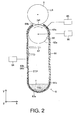
- the toner supply unit 6 is located under the photosensitive drum 3 to face the photosensitive drum 3.
- the toner supply unit 6 is configured to supply the toner T, which is in a charged state, to the electrostatic latent image holding surface LS at a development position DP.
- the development position DP is a position at which the toner supply unit 6 faces the electrostatic latent image holding surface LS. The detailed configuration of the toner supply unit 6 is explained later.
- the paper carrying mechanism 2 includes a pair of registration rollers 21 and a transfer roller 22.
- the registration roller 21 is configured to send the sheet of paper P at predetermined timing toward a position between the transfer roller 22 and the photosensitive drum 3.
- the transfer roller 22 is located such that the sheet of paper P is sandwiched at a transfer position TP between the transfer roller 22 and the photosensitive drum 3. Further, the transfer roller 22 is configured to be rotated in the direction indicated by an arrow in Fig. 1 (i.e., in the counterclockwise direction).
- the transfer roller 22 is connected to a bias power source (not shown) so that a predetermined transfer voltage for transferring the toner adhered on the electrostatic latent image holding surface LS to the sheet of paper P is applied thereto.
- the toner supply unit 6 is configured to supply the charged toner T to the photosensitive drum 3 by carrying the charged toner T through an electric field along a toner transport path TTP.
- a toner box 61 serving as a casing of the toner supply unit 6 is a box type member having an elliptical shape when viewed as a side cross section, and is positioned such that the longer side thereof is in parallel with the vertical direction (i.e., the direction of y-axis).
- the toner T which is dry type powdery developer is accommodated inside the toner box 61. That is, a toner reservoir part 61a is formed by semicylindrical inside space formed at the lower end portion of the toner box 61.
- the toner T has a positive electrostatic property, and is single component black toner having a nonmagnetic property.
- an opening 61b is formed at the top of the toner box 61 (i.e., the position facing the photosensitive drum 3).
- a development roller 62 serving as a developer holding body is accommodated inside the toner box 61.
- the development roller 62 is held by the toner box 61 to be rotatable.
- the development roller 62 is a roller-like member having a toner holding surface 62a which is a cylindrical circumferential surface.
- the development roller 62 is located to face the photosensitive drum 3 through the opening 61b. That is, the toner box 61 and the development roller 62 are located so that, at the development position DP, the toner holding surface 62a of the development roller 62 is located closely to the electrostatic latent image holding surface LS of the photosensitive drum 3 via a gap having a predetermined interval (e.g., approximately 500 ⁇ m).
- a predetermined interval e.g., approximately 500 ⁇ m
- a carrying substrate 63 is provided along the toner transport path TTP.
- the carrying substrate 63 is fixed on the inner wall of the toner box 61.
- the carrying substrate 63 includes a bottom carrying substrate 63a, a vertical carrying substrate 63b and a collecting substrate 63c. The inner configuration of the carrying substrate 63 is explained in detail later.
- the bottom carrying substrate 63a is located at the bottom in the inner space of the toner box 61 to from the bottom surface of the toner reservoir 61a.
- the bottom carrying substrate 63a is formed as a recessed curved surface which is curved to have a semicylindrical shape when viewed as a side cross section. Further, the bottom carrying substrate 63a is formed to smoothly connect to the lower end of the vertical carrying substrate 63b.
- the bottom carrying substrate 63a is connected to the lower end of the vertical carrying substrate 63b so that the toner T in the toner reservoir 61a is carried to the lower end of the vertical carrying substrate 63b.
- the vertical carrying substrate 63b is formed to stand in the vertical direction so that the toner T is carried upwardly in the vertical direction. More specifically, the vertical carrying substrate 63b is configured to carry the toner T supplied from the bottom substrate 63 a toward the development roller 62 and the development position DP in a toner transport direction TTD.
- the vertical carrying substrate 63b is formed such that the upper end of the vertical carrying substrate 63b is located at the position which is higher than the center of the development roller 62. More specifically, the upper end of the vertical carrying substrate 63b is located to reach the opening 61b.
- the upper end of the vertical carrying substrate 63b is formed to be a recessed curved surface to face the cylindrical toner holding surface 62a of the development roller 62 via a gap having a predetermined interval (e.g., approximately 300 ⁇ m).
- the collecting substrate 63c is located to face the development roller 62 at the opposite position with respect to the upper end of the vertical carrying substrate 63b while sandwiching the development roller 62 between the collecting substrate 63c and the upper end of the vertical carrying substrate 63b. That is, the collecting substrate 63c is located on the downstream side in the toner transport direction TTD with respect to the opening 61b of the toner box 61. In this embodiment, the end part of the collecting substrate 63c in the toner transport direction TTD is located at the position corresponding to the position of the lower end of the development roller 62.
- the collecting substrate 63c collects, from the development roller 62, the toner T which has not been consumed at the development position DP, and carries downwardly the collected toner T toward the toner reservoir 61a. More specifically, the upper part of the collecting substrate 63c is formed to be a recessed curved surface to face the outer circumferential surface of the development roller 62 via a gap having a predetermined interval (e.g., approximately 300 ⁇ m which is narrower than the gap formed at the development position DP between the development roller 62 and the photosensitive drum 3). Further, the lower end part of the collecting substrate 63c is located to carry downwardly the toner T.
- a predetermined interval e.g., approximately 300 ⁇ m which is narrower than the gap formed at the development position DP between the development roller 62 and the photosensitive drum 3.
- the bottom carrying substrate 63a and the vertical carrying substrate 63b of the carrying substrate 63 are electrically connected to a carrying power supply circuit 64.
- the collecting substrate 63c is electrically connected to a collecting power supply circuit 65.
- the development roller 62 is electrically connected to a development bias power supply circuit 66.
- Each of the carrying power supply circuit 64, the collecting power supply circuit 65 and the development bias power supply circuit 66 is configured to output an appropriate voltage required to circulate the toner T in the toner transport direction TTD along the toner transport path TTP (i.e., to carry the toner T in the toner reservoir 61a to be held on the development roller 62, to supply the toner T held on the development roller 62 to the development position DP, to collect the toner T which has not been consumed at the development position DP from the development roller 62, and to circulate downwardly the collected toner T to the toner reservoir 61a).
- the carrying power supply circuit 64 outputs an alternating voltage having a rectangular waveform, a voltage of 400V to 1000V (an amplitude of 600V and a DC offset of 700V) and a frequency of 300Hz.
- the collecting power supply circuit 65 outputs an alternating voltage having a rectangular waveform, a voltage of -300V to +300V (an amplitude of 600V and a DC offset of 0V) and a frequency of 300Hz.
- the development bias power supply circuit 66 outputs an alternating voltage having a rectangular waveform, a voltage of -600V to 1400V (an amplitude of 2000V and a DC offset of 400V) and a frequency of 1200Hz.
- the development bias power supply circuit 66 applies, to the development roller 62, the output voltage (i.e., a collecting bias) having the amplitude larger than that of the collecting power supply circuit 65 and having the frequency which is an integral multiple of the frequency of the output voltage of the collecting power supply circuit 65. Furthermore, the collecting power supply circuit 65 applies, to the collecting substrate 63c, the output voltage having an average potential (0V) which is lower than an average potential (240V) of the exposed part on the electrostatic latent image holding surface LS to which the toner T is to be supplied. Furthermore, the output voltages of the collecting power supply circuit 65 and the development bias power supply circuit 66 are set such that the electric field between the development roller 62 and the collecting substrate 63c is stronger than the electric field between the development roller 62 and the photosensitive drum 3.
- the output voltage i.e., a collecting bias
- a shield 67 is provided at a position close to the vertical carrying substrate 63b under the development roller 62 in the inner space of the toner box 61.
- the shield 67 is provided so that when the toner T flying in the inner space of the toner box 61 due to the motion of the carrying substrate 63 is prevented from being adhered to the development roller 62.
- the carrying substrate 63 is a thin plate-like member.
- the carrying substrate 63 has a structure substantially equal to an FPC (Flexible Printed Circuit). More specifically, the carrying substrate 63 includes carrying electrodes 631, an electrode support film 632, an electrode coating 633 and an electrode overcoating 634.
- FPC Flexible Printed Circuit
- the carrying electrodes 631 on the bottom carrying substrate 63a, the carrying electrodes 631 on the vertical carrying substrate 63b, the carrying electrodes 631 on the collecting substrate 63c are frequently referred to as bottom carrying electrodes 631a, vertical carrying electrodes 631b and collecting electrodes 631c, respectively.
- the carrying electrodes 631 are formed as linear patterns, each of which is elongated in parallel with the main scanning direction perpendicular to the auxiliary scanning direction and is formed of copper foil having a thickness of several tens of ⁇ m.
- the plurality of carrying electrodes 631 are aligned in parallel with each other and are arranged in the toner transport path TTP.
- the plurality of carrying electrodes 631 aligned along the toner transport path TTP are connected to power supply circuits VA, VB, VC and VD such that the carrying electrodes 631 are connected to the same power supply circuit at every four intervals. That is, the carrying electrode connected to the power supply circuit VA, the carrying electrode connected to the power supply circuit VB, the carrying electrode connected to the power supply circuit VC, the carrying electrode connected to the power supply circuit VD, the carrying electrode connected to the power supply circuit VA, the carrying electrode connected to the power supply circuit VB, the carrying electrode connected to the power supply circuit VC and the carrying electrode connected to the power supply circuit VD ... are repeatedly arranged in this order along the toner transport path TTP. It should be noted that the power supply circuits VA, VB, VC and VD are provided in each of the carrying power supply circuit 64 and the collecting power supply circuit 65.
- the power supply circuits VA to VD output substantially the same driving voltages (i.e., alternating voltages).
- the phases of the output voltages of the power supply circuits VA to VD are shift with respect to each other by 90°. That is, in the order of the output signals of the power supply circuits VA to VD, each of the voltage phases of the output signals delays by 90°.
- the carrying substrate 63 By applying the above described driving voltages to the carrying electrodes 631, the carrying substrate 63 generates a traveling electric field along the toner transport path TTP so that the positively charged toner T is carried in the toner transport direction TTD.
- the plurality of carrying electrodes 631 are formed on the electrode support film 632.
- the electrode support film 632 is an elastic film, for example, made of insulating synthetic resin such as polyimide resin.
- the electrode coating 633 is made of insulating synthetic resin.
- the electrode coating 633 is provided to cover the carrying electrodes 631 and a surface of the electrode support film 632 on which the carrying electrodes 631 are formed.
- the electrode overcoating 634 is formed on the electrode coating 633.
- the electrode overcoating 634 formed on the bottom carrying substrate 63a, the electrode overcoating 634 formed on the vertical carrying substrate 63b and the electrode overcoating 634 formed on the collecting substrate 63c are frequently referred to as a bottom overoating 634a, a vertical overcoating 634b, a collecting overcoating 634c, respectively. That is, the electrode coating 633 is formed between the electrode overcoating 634 and the carrying electrodes 631.
- a surface of the electrode overcoating 634 is formed to be a smooth flat surface without bumps and dips so that the toner T can be carried smoothly.
- the vertical overcoating 634b and the collecting overcoating 634c are made of the same material (e.g., polyester). That is, as the material of the vertical overcoating 634b and the collecting overcoating 634c, material having a triboelectrification position on the plus side in the triboelectrification order with respect to the material (polyimide) of the bottom overcoating 634a is adopted. That is, the material of the vertical overcoating 634b and the collecting overcoating 634c has the same electrification polarity as that of the material of the toner T with respect to the material of the bottom overcoating 634a.
- the material of the vertical overcoating 634b and the collecting overcoating 634c has the same electrification polarity as that of the material of the toner T with respect to the material of the bottom overcoating 634a.
- the leading edge of the sheet of paper P placed on the paper supply tray (not shown) is carried to the registration roller 21. Then, skew of the sheet of paper P is corrected, and the carrying timing is adjusted. Thereafter, the sheet of paper P is carried to the transfer position TP.
- the electrostatic latent image holding surface LS of the photosensitive drum 3 is charged by the charger 4 positively and uniformly.
- the electrostatic latent image holding surface LS charged by the charger 4 moves along the auxiliary scanning direction by rotation in the direction indicated by the arrow in Fig. 1 to reach the scan position SP facing the scanning unit 5.
- the laser beam LB modulated by image information scans on the electrostatic latent image holding surface LS in the main scanning direction.
- the positive charges of the electrostatic latent image holding surface LS are partially removed.
- a pattern of the positive charges appears as an electrostatic latent image.
- the electrostatic latent image formed on the electrostatic latent image holding surface LS moves to the development position DP facing the toner supply unit 6 by rotation of the photosensitive drum 3 in the direction indicated y the arrow in Fig. 1 (i.e., in the clockwise direction).
- the toner T stored in the toner box61 charges, for example, by contact and friction with respect to the bottom overcoating 634a of the bottom carrying substrate 63a.
- the charged toner T which contacts or is situated closely to the bottom overcoating 634a of the bottom carrying substrate 63a is carried in the toner transport direction TTD by the electric field generated by the voltage applied to the bottom carrying substrate 631a, and is passed to the vertical carrying substrate 63b.
- the downstream end portion of the bottom carrying substrate 63a along the toner transport direction TTD i.e., a connection part of the bottom carrying substrate 63a with respect to the vertical carrying substrate 63b
- TTD toner transport direction
- the vertical carrying substrate 63b carries upward the toner T which has been passed at the lower end portion thereof from the bottom carrying substrate 63a. Since the vertical overcoating 634b of the vertical carrying substrate 63b has the lower degree of effect of further charging positively the toner T that that of the bottom overcoating 634a of the bottom carrying substrate 63a, it becomes possible to prevent the charged state of the toner T being carried along the vertical carrying substrate 63b from being altered.
- toner not properly charged e.g., toner charged negatively or non-charged toner
- toner not properly charged due to gravity or an electric field generated between the vertical carrying substrate 63b and the development roller 62, the toner not properly charged falls downward when the toner T is carried upward in the vertical direction along the vertical carrying substrate 63b or when the toner T is attracted toward the development roller 62 by the electric field acting between the vertical carrying substrate 63b and the development roller 62.
- the toner which has fallen downward from the vertical carrying substrate 63b reaches the downstream side end of the bottom carrying substrate 63a along the toner transport direction TTD.
- the toner T situated around the downstream side end of the bottom carrying substrate 63a along the toner transport direction TTD is suitably fluidized, and therefore is suitably charged by friction with the bottom overcoating 634a.
- the toner T can be suitably carried without the need for forcibly charging the toner T in the toner reservoir 61a through the mechanical effect by a stirring member such as a blade. Therefore, deterioration with time of the toner can be suppressed.
- the toner which is not properly charged and has fallen from the vertical carrying substrate 63b reaches directly to the toner reservoir 61a, but not the midway of the vertical carrying substrate 63b. Therefore, it becomes possible to prevent the flow of the toner T by the vertical carrying substrate 63b from being disturbed. For example, removal of the suitably charged toner T from the vertical carrying substrate 63b, and retention and deposition of the not properly charged toner T on the vertical carrying substrate 63b can be prevented.
- the positively charged toner T is thus supplied to the development position DP.
- the electrostatic latent image formed on the electrostatic latent image holding surface LS is developed with the toner T. That is, the toner T adheres to a part of the electrostatic latent image holding surface LS where positive charges of the electrostatic latent image are removed.
- an image formed by the toner T (hereafter, referred to as a toner image) is held on the electrostatic latent image holding surface LS.
- the toner T which is held on the toner holding surface 62a and has passed the development position DP moves to the side of the collecting substrate 63c by the effect of the collecting bias. That is, the toner T not consumed at the development position DP is collected from the toner holding surface 62a by the collecting substrate 63c.
- an alternating bias is applied to the development roller 62.
- the toner T adjacent to the toner holding surface 62a of the development roller 62 vibrates.
- the toner T raised from the toner holding surface 62a collides with the toner T adhered to the toner holding surface 62a.
- the toner T adhered to the toner holding surface 62a is brought to a state where the toner T can be easily raised from the toner holding surface 62a.
- the average potential (0V) of the collecting bias is lower than the potential (240V) of the exposed part which is formed on the electrostatic latent image holding surface LS and to which the toner T is to be supplied. Furthermore, in this embodiment, the electric field between the development roller 62 and the collecting substrate 63c is stronger than the electric field between the development roller 62 and the photosensitive drum 3.
- the toner T which has not been consumed at the development position DP is adequately removed from the toner holding surface 62a and is moved to the side of the collecting substrate 63c. Consequently, it becomes possible to appropriately prevent a ghost image from occurring on a formed image.
- the amplitude of the collecting bias is larger than the amplitude of the voltage applied to the collecting electrodes 631c. Therefore, it is possible to suitably collect the toner T from the toner holding surface 62a without increasing the voltage between adjacent ones of the collecting electrodes 631c. That is, it is possible to suitably maintain insulation between adjacent ones of the collecting electrodes 631c.
- the collecting bias also serves as a bias for a so-called jumping phenomenon at the development position DP.
- the collecting bias can be suitably applied with a relatively simple structure.
- the toner T moved from the toner holding surface 62a to the side of the collecting substrate 63c is carried to the downwardly located ink reservoir 61a by the electric field generated by the voltage applied to the collecting electrodes 631c.
- the frequency of the collecting bias is set to an integral multiple of the frequency of the voltage applied to the vertical carrying electrodes 631b or the collecting electrodes 631c. Therefore, the electric field of the collecting bias and the electric field for carrying the toner T along the collecting substrate 63c can be suitably synchronized with respect to each other.
- the toner T is carried downwardly in the vertical direction.
- the inertia having the same direction as that of gravity acts on the toner T.
- the toner T falls toward the toner reservoir 61a by the effect of the gravity and the inertia having the same direction as that of the gravity. Therefore, the toner T suitably circulates to the toner reservoir 61a even when the collecting substrate 63c is not formed to reach the toner reservoir 61a.
- the toner image held on the electrostatic latent image holding surface LS is carried to the transfer position TP by rotation of the electrostatic latent image holding surface LS in the direction indicated by the arrow (i.e., in the clockwise direction).
- the toner image is transferred to the sheet of paper P.
- a toner supply unit 6B of the second embodiment is a variation of the toner supply unit 6 of the first embodiment and a laser printer according to the second embodiment has substantially the same configuration as that shown in Fig. 1 , the following explanation focuses on features of the second embodiment.
- Figs. 5 and 6 to elements which are substantially the same as those of the first embodiment, the same reference numbers are assigned, and explanations thereof will not be repeated.
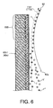
- an upper end part 63b1 of the vertical carrying substrate 63b is situated at the position substantially equal to the height of the center of the development roller 62.
- a carry stop area 635 is provided at the uppermost part of the upper end part 63b1 in the toner transport direction TTD.
- the carry stop area 635 is formed in an area from the uppermost end of the vertical carrying substrate 63b to the position at which the vertical carrying substrate 63b is closest to the toner holding surface 62a.
- the carry stop area 635 is configured not to generate the electric field for carrying the toner T in the toner transport direction TTD.
- a plurality of carry stop electrodes 636 are provided in the carry stop area 635. That is, parts of the electrodes 631b formed at the downstream end portion on the vertical carrying substrate 63b are used as the carry stop electrodes 636. Therefore, the carry stop electrodes 636 are provided along the toner transport path TTP.
- Each of the carry stop electrodes 636 is formed as a liner pattern elongated in parallel with the main scanning direction, and is formed of copper foil having a thickness of several tens of ⁇ m.
- the carry stop electrodes 636 To the carry stop electrodes 636, a polyphase alternating voltage having the inverse traveling direction with respect to the traveling direction of the voltage for the carrying electrodes 631 shown in Fig. 4 is applied. That is, the carry stop area 635 has the function of carrying the toner T in the inverse direction of the toner transport direction TTD.
- toner not properly charged e.g., non-charged toner T' and inversely charged (negatively charged) toner T
- toner not properly charged e.g., non-charged toner T' and inversely charged (negatively charged) toner T
- toner T properly charged can be supplied to the toner holding surface 62a of the development roller 62.
- the non-charged toner T' falls downward from the vertical carrying substrate 63b by the effect of gravity.
- the negatively charged toner T" also falls downward by the effect of the bias between the vertical carrying substrate 62b and the development roller 62, the electric field generated on the carry stop area 635, and the effect of gravity.
- the toner T suitably charged is selectively supplied to the development roller 62 and the development position DP. That is, on the vertical carrying substrate 63b, the toner not properly charged is separated from the toner T suitably charged.
- the developer supply device satisfies a following relationship: Dg > Dh .
- Vh denotes an average potential of the plurality of collecting electrodes
- VL denotes a potential of a part on the supply target to which the developer is to be supplied
Landscapes
- Physics & Mathematics (AREA)
- General Physics & Mathematics (AREA)
- Dry Development In Electrophotography (AREA)
Applications Claiming Priority (3)
| Application Number | Priority Date | Filing Date | Title |
|---|---|---|---|
| JP2008325322A JP4618373B2 (ja) | 2008-12-22 | 2008-12-22 | 現像剤供給装置 |
| JP2008325313A JP4661955B2 (ja) | 2008-12-22 | 2008-12-22 | 現像剤供給装置 |
| JP2008325320A JP4618372B2 (ja) | 2008-12-22 | 2008-12-22 | 現像剤供給装置 |
Publications (2)
| Publication Number | Publication Date |
|---|---|
| EP2199872A2 true EP2199872A2 (de) | 2010-06-23 |
| EP2199872A3 EP2199872A3 (de) | 2010-12-22 |
Family
ID=41835789
Family Applications (1)
| Application Number | Title | Priority Date | Filing Date |
|---|---|---|---|
| EP09180328A Withdrawn EP2199872A3 (de) | 2008-12-22 | 2009-12-22 | Entwicklerzufuhrvorrichtung |
Country Status (3)
| Country | Link |
|---|---|
| US (1) | US8326188B2 (de) |
| EP (1) | EP2199872A3 (de) |
| CN (1) | CN101763011B (de) |
Cited By (1)
| Publication number | Priority date | Publication date | Assignee | Title |
|---|---|---|---|---|
| EP2317400A3 (de) * | 2009-10-30 | 2011-09-28 | Brother Kogyo Kabushiki Kaisha | Entwicklerzufuhrvorrichtung und diese aufweisende Bilderstellungsvorrichtung |
Families Citing this family (7)
| Publication number | Priority date | Publication date | Assignee | Title |
|---|---|---|---|---|
| JP4911217B2 (ja) * | 2009-10-30 | 2012-04-04 | ブラザー工業株式会社 | 現像剤供給装置 |
| JP4900467B2 (ja) * | 2009-12-24 | 2012-03-21 | ブラザー工業株式会社 | 現像剤供給装置 |
| JP5045775B2 (ja) * | 2010-03-23 | 2012-10-10 | ブラザー工業株式会社 | 現像剤供給装置 |
| JP5560939B2 (ja) * | 2010-06-17 | 2014-07-30 | ブラザー工業株式会社 | 現像剤供給装置 |
| JP5540970B2 (ja) * | 2010-07-30 | 2014-07-02 | ブラザー工業株式会社 | 現像剤供給装置 |
| JP2012163593A (ja) | 2011-02-03 | 2012-08-30 | Brother Ind Ltd | 現像剤供給装置 |
| JP2012177791A (ja) * | 2011-02-25 | 2012-09-13 | Brother Ind Ltd | 現像剤供給装置 |
Citations (8)
| Publication number | Priority date | Publication date | Assignee | Title |
|---|---|---|---|---|
| JPS6161236A (ja) | 1984-09-03 | 1986-03-29 | Hitachi Ltd | 光学式デイスク再生装置 |
| US5142336A (en) | 1989-06-09 | 1992-08-25 | Minolta Camera Kabushiki Kaisha | Developer having the predetermined residual polarization and developing apparatus for using the developer |
| JPH04299155A (ja) | 1991-03-28 | 1992-10-22 | Casio Comput Co Ltd | 静電記録装置 |
| US6272305B1 (en) * | 1999-11-26 | 2001-08-07 | Xerox Corporation | Apparatus for developing a latent image |
| US6272296B1 (en) | 1999-12-10 | 2001-08-07 | Xerox Corporation | Method and apparatus using traveling wave potential waveforms for separation of opposite sign charge particles |
| JP2004341311A (ja) | 2003-05-16 | 2004-12-02 | Sharp Corp | 現像装置及びそれを備えた画像形成装置 |
| JP2005173456A (ja) * | 2003-12-15 | 2005-06-30 | Ricoh Co Ltd | トナー搬送装置、現像装置、プロセスユニット及び画像形成装置 |
| WO2008026718A1 (fr) * | 2006-08-28 | 2008-03-06 | Brother Kogyo Kabushiki Kaisha | Dispositif de formation d'image |
Family Cites Families (15)
| Publication number | Priority date | Publication date | Assignee | Title |
|---|---|---|---|---|
| JPS59181371A (ja) * | 1983-03-31 | 1984-10-15 | Toshiba Corp | 現像装置 |
| JPS60115962A (ja) | 1983-11-28 | 1985-06-22 | Olympus Optical Co Ltd | 複写機の現像装置 |
| JPH01184862A (ja) | 1988-01-13 | 1989-07-24 | Matsushita Electric Ind Co Ltd | 半導体装置の製造方法 |
| US5027157A (en) | 1988-12-02 | 1991-06-25 | Minolta Camera Kabushiki Kaisha | Developing device provided with electrodes for inducing a traveling wave on the developing material |
| JPH02160266A (ja) | 1988-12-14 | 1990-06-20 | Minolta Camera Co Ltd | 電界カーテン装置 |
| JPH0594084A (ja) | 1991-10-01 | 1993-04-16 | Minolta Camera Co Ltd | 現像装置 |
| JPH06161236A (ja) | 1992-11-24 | 1994-06-07 | Hiraoka H I Kenkyusho:Kk | 現像装置 |
| JPH1184862A (ja) | 1997-09-16 | 1999-03-30 | Minolta Co Ltd | 電界カーテン装置及び現像装置 |
| JP2001122436A (ja) | 1999-10-20 | 2001-05-08 | Canon Inc | 搬送装置及び画像形成装置 |
| JP2002287495A (ja) | 2001-03-23 | 2002-10-03 | Ricoh Co Ltd | 静電搬送装置、現像装置、画像形成装置及び分級装置 |
| JP3845593B2 (ja) | 2002-03-13 | 2006-11-15 | 株式会社リコー | 分級装置、現像装置、画像形成装置、分級方法、現像方法及び画像形成方法 |
| JP2004069903A (ja) * | 2002-08-05 | 2004-03-04 | Ricoh Co Ltd | 現像装置及び画像形成装置 |
| JP2004279880A (ja) | 2003-03-18 | 2004-10-07 | Ricoh Co Ltd | 現像装置、画像形成装置及びプロセスカートリッジ |
| JP4400604B2 (ja) * | 2006-09-15 | 2010-01-20 | ブラザー工業株式会社 | 現像剤供給装置及び画像形成装置 |
| JP2009080271A (ja) * | 2007-09-26 | 2009-04-16 | Brother Ind Ltd | 現像剤搬送装置および画像形成装置 |
-
2009
- 2009-12-22 CN CN200910261182.7A patent/CN101763011B/zh not_active Expired - Fee Related
- 2009-12-22 US US12/645,290 patent/US8326188B2/en not_active Expired - Fee Related
- 2009-12-22 EP EP09180328A patent/EP2199872A3/de not_active Withdrawn
Patent Citations (8)
| Publication number | Priority date | Publication date | Assignee | Title |
|---|---|---|---|---|
| JPS6161236A (ja) | 1984-09-03 | 1986-03-29 | Hitachi Ltd | 光学式デイスク再生装置 |
| US5142336A (en) | 1989-06-09 | 1992-08-25 | Minolta Camera Kabushiki Kaisha | Developer having the predetermined residual polarization and developing apparatus for using the developer |
| JPH04299155A (ja) | 1991-03-28 | 1992-10-22 | Casio Comput Co Ltd | 静電記録装置 |
| US6272305B1 (en) * | 1999-11-26 | 2001-08-07 | Xerox Corporation | Apparatus for developing a latent image |
| US6272296B1 (en) | 1999-12-10 | 2001-08-07 | Xerox Corporation | Method and apparatus using traveling wave potential waveforms for separation of opposite sign charge particles |
| JP2004341311A (ja) | 2003-05-16 | 2004-12-02 | Sharp Corp | 現像装置及びそれを備えた画像形成装置 |
| JP2005173456A (ja) * | 2003-12-15 | 2005-06-30 | Ricoh Co Ltd | トナー搬送装置、現像装置、プロセスユニット及び画像形成装置 |
| WO2008026718A1 (fr) * | 2006-08-28 | 2008-03-06 | Brother Kogyo Kabushiki Kaisha | Dispositif de formation d'image |
Cited By (2)
| Publication number | Priority date | Publication date | Assignee | Title |
|---|---|---|---|---|
| EP2317400A3 (de) * | 2009-10-30 | 2011-09-28 | Brother Kogyo Kabushiki Kaisha | Entwicklerzufuhrvorrichtung und diese aufweisende Bilderstellungsvorrichtung |
| US8494420B2 (en) | 2009-10-30 | 2013-07-23 | Brother Kogyo Kabushiki Kaisha | Development agent supply device and image forming apparatus having the same |
Also Published As
| Publication number | Publication date |
|---|---|
| US20100158577A1 (en) | 2010-06-24 |
| US8326188B2 (en) | 2012-12-04 |
| EP2199872A3 (de) | 2010-12-22 |
| CN101763011B (zh) | 2013-01-30 |
| CN101763011A (zh) | 2010-06-30 |
Similar Documents
| Publication | Publication Date | Title |
|---|---|---|
| US8326188B2 (en) | Developer supply device | |
| US8095052B2 (en) | Developer supply device | |
| US8311462B2 (en) | Developer supply device | |
| US8275298B2 (en) | Developer supply device | |
| US8326190B2 (en) | Substrate configuration for a developer supply device | |
| JP4618372B2 (ja) | 現像剤供給装置 | |
| JP4661955B2 (ja) | 現像剤供給装置 | |
| US8112019B2 (en) | Developer supply device | |
| JP4618373B2 (ja) | 現像剤供給装置 | |
| JP4911188B2 (ja) | 現像剤供給装置 | |
| JP5531882B2 (ja) | 現像剤供給装置 | |
| JP5070575B2 (ja) | 現像剤供給装置 | |
| JP5093255B2 (ja) | 現像剤供給装置 | |
| JP5560939B2 (ja) | 現像剤供給装置 | |
| JP4978683B2 (ja) | 現像剤供給装置 | |
| JP4798402B2 (ja) | 現像剤供給装置 | |
| JP2011118345A (ja) | 現像剤供給装置 | |
| JP2010224458A (ja) | 現像剤供給装置 | |
| JP2010224462A (ja) | 現像剤供給装置 | |
| US8050600B2 (en) | Image formation device and developer supplying device | |
| JP2010224449A (ja) | 現像剤供給装置 | |
| JP2010224467A (ja) | 現像剤供給装置 | |
| JP2011064843A (ja) | 現像剤供給装置 | |
| JP2011095529A (ja) | 現像剤供給装置 | |
| JP2011022375A (ja) | 現像剤供給装置 |
Legal Events
| Date | Code | Title | Description |
|---|---|---|---|
| PUAI | Public reference made under article 153(3) epc to a published international application that has entered the european phase |
Free format text: ORIGINAL CODE: 0009012 |
|
| AK | Designated contracting states |
Kind code of ref document: A2 Designated state(s): AT BE BG CH CY CZ DE DK EE ES FI FR GB GR HR HU IE IS IT LI LT LU LV MC MK MT NL NO PL PT RO SE SI SK SM TR |
|
| AX | Request for extension of the european patent |
Extension state: AL BA RS |
|
| PUAL | Search report despatched |
Free format text: ORIGINAL CODE: 0009013 |
|
| AK | Designated contracting states |
Kind code of ref document: A3 Designated state(s): AT BE BG CH CY CZ DE DK EE ES FI FR GB GR HR HU IE IS IT LI LT LU LV MC MK MT NL NO PL PT RO SE SI SK SM TR |
|
| AX | Request for extension of the european patent |
Extension state: AL BA RS |
|
| 17P | Request for examination filed |
Effective date: 20110622 |
|
| 17Q | First examination report despatched |
Effective date: 20160317 |
|
| STAA | Information on the status of an ep patent application or granted ep patent |
Free format text: STATUS: THE APPLICATION IS DEEMED TO BE WITHDRAWN |
|
| 18D | Application deemed to be withdrawn |
Effective date: 20160728 |