EP2189986A1 - Verzögerungseinstellungsvorrichtung, Halbleitervorrichtung und Verzögerungseinstellungsverfahren - Google Patents
Verzögerungseinstellungsvorrichtung, Halbleitervorrichtung und Verzögerungseinstellungsverfahren Download PDFInfo
- Publication number
- EP2189986A1 EP2189986A1 EP09174000A EP09174000A EP2189986A1 EP 2189986 A1 EP2189986 A1 EP 2189986A1 EP 09174000 A EP09174000 A EP 09174000A EP 09174000 A EP09174000 A EP 09174000A EP 2189986 A1 EP2189986 A1 EP 2189986A1
- Authority
- EP
- European Patent Office
- Prior art keywords
- signal
- data
- data strobe
- delay
- circuit
- Prior art date
- Legal status (The legal status is an assumption and is not a legal conclusion. Google has not performed a legal analysis and makes no representation as to the accuracy of the status listed.)
- Granted
Links
Images




Classifications
-
- G—PHYSICS
- G11—INFORMATION STORAGE
- G11C—STATIC STORES
- G11C7/00—Arrangements for writing information into, or reading information out from, a digital store
- G11C7/22—Read-write [R-W] timing or clocking circuits; Read-write [R-W] control signal generators or management
- G11C7/225—Clock input buffers
-
- G—PHYSICS
- G11—INFORMATION STORAGE
- G11C—STATIC STORES
- G11C11/00—Digital stores characterised by the use of particular electric or magnetic storage elements; Storage elements therefor
- G11C11/21—Digital stores characterised by the use of particular electric or magnetic storage elements; Storage elements therefor using electric elements
- G11C11/34—Digital stores characterised by the use of particular electric or magnetic storage elements; Storage elements therefor using electric elements using semiconductor devices
- G11C11/40—Digital stores characterised by the use of particular electric or magnetic storage elements; Storage elements therefor using electric elements using semiconductor devices using transistors
- G11C11/401—Digital stores characterised by the use of particular electric or magnetic storage elements; Storage elements therefor using electric elements using semiconductor devices using transistors forming cells needing refreshing or charge regeneration, i.e. dynamic cells
- G11C11/4063—Auxiliary circuits, e.g. for addressing, decoding, driving, writing, sensing or timing
- G11C11/407—Auxiliary circuits, e.g. for addressing, decoding, driving, writing, sensing or timing for memory cells of the field-effect type
-
- G—PHYSICS
- G11—INFORMATION STORAGE
- G11C—STATIC STORES
- G11C11/00—Digital stores characterised by the use of particular electric or magnetic storage elements; Storage elements therefor
- G11C11/21—Digital stores characterised by the use of particular electric or magnetic storage elements; Storage elements therefor using electric elements
- G11C11/34—Digital stores characterised by the use of particular electric or magnetic storage elements; Storage elements therefor using electric elements using semiconductor devices
- G11C11/40—Digital stores characterised by the use of particular electric or magnetic storage elements; Storage elements therefor using electric elements using semiconductor devices using transistors
- G11C11/401—Digital stores characterised by the use of particular electric or magnetic storage elements; Storage elements therefor using electric elements using semiconductor devices using transistors forming cells needing refreshing or charge regeneration, i.e. dynamic cells
- G11C11/4063—Auxiliary circuits, e.g. for addressing, decoding, driving, writing, sensing or timing
- G11C11/407—Auxiliary circuits, e.g. for addressing, decoding, driving, writing, sensing or timing for memory cells of the field-effect type
- G11C11/4076—Timing circuits
-
- G—PHYSICS
- G11—INFORMATION STORAGE
- G11C—STATIC STORES
- G11C29/00—Checking stores for correct operation ; Subsequent repair; Testing stores during standby or offline operation
- G11C29/02—Detection or location of defective auxiliary circuits, e.g. defective refresh counters
-
- G—PHYSICS
- G11—INFORMATION STORAGE
- G11C—STATIC STORES
- G11C7/00—Arrangements for writing information into, or reading information out from, a digital store
- G11C7/10—Input/output [I/O] data interface arrangements, e.g. I/O data control circuits, I/O data buffers
- G11C7/1051—Data output circuits, e.g. read-out amplifiers, data output buffers, data output registers, data output level conversion circuits
- G11C7/1066—Output synchronization
-
- G—PHYSICS
- G11—INFORMATION STORAGE
- G11C—STATIC STORES
- G11C7/00—Arrangements for writing information into, or reading information out from, a digital store
- G11C7/22—Read-write [R-W] timing or clocking circuits; Read-write [R-W] control signal generators or management
-
- G—PHYSICS
- G11—INFORMATION STORAGE
- G11C—STATIC STORES
- G11C7/00—Arrangements for writing information into, or reading information out from, a digital store
- G11C7/22—Read-write [R-W] timing or clocking circuits; Read-write [R-W] control signal generators or management
- G11C7/222—Clock generating, synchronizing or distributing circuits within memory device
-
- G—PHYSICS
- G11—INFORMATION STORAGE
- G11C—STATIC STORES
- G11C2207/00—Indexing scheme relating to arrangements for writing information into, or reading information out from, a digital store
- G11C2207/22—Control and timing of internal memory operations
- G11C2207/2254—Calibration
Definitions
- the present invention relates to delay adjustment between a memory and a memory controller, and particularly to delay adjustment between a DDR SDRAM (Double Data Rate Synchronous Dynamic Random Access Memory) and a memory controller.
- DDR SDRAM Double Data Rate Synchronous Dynamic Random Access Memory
- a DDR SDRAM is a memory including a high-speed transfer function.
- the DDR SDRAM can read and write data on both the rising and falling edges of the clock signal for synchronization between circuits. That is to say, the DDR SDRAM inputs and outputs data with twice the frequency of an external clock. Therefore, the DDR SDRAM has a narrower data width (width of determined data), at which data can be reliably read, than that of SDR SDRAM. It is also necessary to notify a timing to read data output from the DDR SDRAM correctly.
- the DDR DRAM uses a data strobe signal (DQS).
- the data strobe signal is a signal to notify a timing to transfer data.
- the DDR SDRAM outputs a data signal (DQ) and the data strobe signal at the same time.
- a requestor requesting data transfer receives the data signal and the data strobe signal in response to issuance of a read command.
- the requestor retrieves data from the data signal in accordance with the data strobe signal.
- a memory controller is employed. The memory controller is placed between the memory and the requestor, and includes general functions to control the operation of memory access.
- the memory controller having a configuration in which a delay of the flight time in considered to determine a timing to receive the data strobe signal,
- the flight time varies depending on implementation conditions, such as the length of a line between the memory and the memory controller. For this reason, the reception timing is not determined uniquely in the process of designing the memory controller. It is necessary to incorporate a function (for example, a circuit) for dealing with a certain range of flight time in the memory controller.
- Japanese Unexamined Patent Application Publication No. 2005-276396 discloses a technique of adjusting a delay time using an expected value at initialization of a device.
- a calibration pattern is formed in a memory, and PASS/FAIL determination is performed using the formed pattern as the expected value at the initialization of the device. Then, the delay time is adjusted to be optimized based on the determination result.
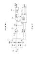
- Fig. 6 is a circuit diagram showing a configuration of a memory interface control circuit disclosed in Japanese Unexamined Patent Application Publication No. 2005-276396 .
- the circuit disclosed in Japanese Unexamined Patent Application Publication No. 2005-276396 is a circuit which performs the functions as noted below.
- the circuit generates in the inside thereof a timing of retrieving the DQS, actually performs read and write operation on the DRAM, and checks an expectation value in order to confirm whether retrieved data is correct or not.
- the circuit selects an optimal timing after repetition of generating the timing of retrieving the DQS while gradually shifting the timing of retrieving the DQS.
- Japanese Unexamined Patent Application Publication No. 2003-223786 discloses a circuit incorporating a comparator to detect a timing of starting point of preamble. The timing of starting point of preamble indicates a change from an impedance state to a low level state.
- Fig. 7 shows a data strobe receiver disclosed in Japanese Unexamined Patent Application Publication No. 2003-223786 .
- Japanese Unexamined Patent Application Publication No. 2008-103013 discloses a technique of eliminating unstable operation caused by a variation in delay of the data strobe signal.
- Fig. 8 is a diagram showing a configuration of a memory read controller disclosed in Japanese Unexamined Patent Application Publication No. 2008-103013 .
- the memory read controller controls a pull up circuit 11s to pull-up the data strobe signal when a read request signal turns active.
- a signal changes from high level to low level, Input of the DQS is enabled valid by an enable signal of a control circuit 14s. Then, the input of DQS is disabled by the enable signal of the control circuit 14s after edges of the DQS signal are counted by the number of burst lengths.
- the circuit disclosed in Japanese Unexamined Patent Application Publication No. 2005-276396 requires a circuit to preliminarily write a calibration pattern to a memory, and a comparison circuit to compare data read from a memory, resulting in an increase in circuit size.
- control circuit disclosed in Japanese Unexamined Patent Application Publication No. 2003-223786 becomes large, because the circuit needs to be added with a comparator for requesting independent 2nd Vref and a voltage supply.
- the control circuits disclosed in Japanese Unexamined Patent Application Publication Nos. 2003-223786 and 2008-103013 also detect the timing of retrieving the DQS signal, but do not recognize the flight time. In the configuration in which the flight time is not recognized, it is necessary to reset the clock in order to transfer data to the subsequent-stage, circuit, (requestor). In these cases, the control circuits use a FIFO, for example, which results in an increase in circuit size.
- the flight time between the memory and the memory controller cannot be calculated in design phase because the flight time varies depending on the length of a line. Therefore, the memory controller requires a circuit to adjust the Sight time.
- the present inventor has found a problem that the size of a circuit for adjusting the flight time is increased. Since the provision of a circuit for adjusting the flight time increases the size of the whole circuit, it is an object of the present invention to provide a delay adjustment device, a semiconductor device or a respective method allowing to downsize the circuit for adjusting the flight time and/or contribute to reduce the size of the whole circuit.
- a first exemplary aspect of an embodiment of the present invention is a delay adjustment device that is connected a memory, and adjusts a timing to retrieve data with a data signal and a data strobe signal output from the memory, the delay adjustment device including: a data retrieve unit that receives the data signal and the data strobe signal, and outputs data value of the data signal in accordance with the data strobe signal; and a control unit that issues a read command to the memory, retrieves values of the data strobe signal in response to the read command to calculate a flight time, and controls a valid period of the data strobe signal based on the flight time, The control unit issues me read command, retrieves values of a plurality of data strobe signals in response to the read command, and then calculates the flight time using the values of the plurality of data strobe signals.
- the use of the flight time makes it possible to predict an arrival time of the data signal and the data strobe signal at the data retrieve unit, with accuracy. Therefore, a circuit that estimates the flight time using the data strobe signal is implemented. As a result, it is expected to downsize the circuit as compared to a circuit that estimates the flight time using the data signal.
- a second exemplary aspect of an embodiment of the present invention is a semiconductor device including: the delay adjustment device as referred to above; and a processing unit that processes a data value output from the delay adjustment device.
- the delay adjustment device as referred to above, it is expected to the whole circuit of the semiconductor device. It is also possible to retrieve the data value of the data signal in synchronization with the internal clock signal, when the internal clock signal used by the processing unit is used for the delay adjustment device.
- a third exemplary aspect of an embodiment of the present invention is a delay adjustment method of a delay adjustment device that is connected to a memory and adjusts a timing to retrieve data with a data signal and a data strobe signal output from the memory, in response to a read command, the delay adjustment method including: issuing the read command to the memory; retrieving values of the data strobe signal at different timings in accordance with the read command; calculating a flight time using values of a plurality of data strobe signals retrieved; and controlling a valid period of the data strobe signal based on the flight time.
- a DDR SDRAM is used as an exemplary memory.
- a delay adjustment device calculates flight time using a data strobe signal output from the DDR SDRAM, and adjusts a timing to retrieve a data value from data signals properly.
- the following exemplary embodiments will be described by using a delay adjustment circuit as an example of the delay adjustment device.
- a device (circuit) which issues a memory access request (for example, a read command) is also referred to as a requestor, a processing circuits, or an internal circuit It is assumed that the requestor accesses the memory through a memory controller.
- the memory controller is a device (circuit) which has a function to control memory access, for example,
- the delay adjustment device according to this exemplary embodiment may implement part of the function of the memory controller.
- the DDR SDRAM outputs a data signal and a data strobe signal in response to the read command.
- the data signal (hereinafter also referred to as "DQ”) is a signal which transfers data in response to the read command.
- the data strobe signal (hereinafter also referred to as "DQS”) is a signal which notifies a timing to transfer data, and is output from the memory together with the data signal.
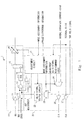
- Fig. 1 is a block diagram showing an example of a configuration of a delay adjustment device (delay adjustment circuit) according to the first exemplary embodiment, of the present invention.
- a delay adjustment circuit 1 includes a data retrieve unit 10 and a control unit 20.
- the data retrieve unit 10 receives the data signal and data strobe signal from the DDR SDRAM, and outputs the data value of the data signal in accordance with the data strobe signal.
- the control unit 20 controls the timing for the data retrieve unit 10 to output the data value. Specifically, the data retrieve unit 10 is controlled such that the control unit 20 adjusts a valid period of the data strobe signal.
- the control unit 20 calculates the flight time using the data strobe signal. Specifically, the control unit 20 issues the read command to the DDR SDRAM, and retrieves the value of the data strobe signal (hereinafter also referred to as "strobe value"). The control unit 20 then calculates the flight time using the value of the data strobe signal thus obtained. The control unit 20 also controls the valid period of the data strobe signal based on the calculated flight time. Namely, the control unit 20 notifies the data retrieve unit 10 of the valid period of the data strobe signal to thereby control the timing for the data retrieve unit 10 to output the data value in accordance with the data strobe signal. Details of the data retrieve unit 10 and the control unit 20 will be described later. Fig.
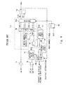
- FIG. 2 is a block diagram showing an example of a configuration of a DDR SDRAM 9 and a semiconductor device 8 incorporating the delay adjustment circuit 1 shown in Fig. 1 .
- the semiconductor device 8 includes the delay adjustment circuit 1 and a processing circuit 7.
- Symbols A to H indicate signals in Fig. 2 and are used later in the description of Fig. 5 .
- Elements of a memory controller which have no relationship to the present invention are omitted in Fig. 2 .
- the processing circuit 7 issues a command, reads desired data from the DDR SDRAM 9, and uses the read data.
- the processing circuit 7 is also referred to as a requestor because the processing circuit 7 requests the DDR SDRAM 9 to send data, by issuing the read command.
- the processing unit 7 includes a flip-flop 71.
- the flip-flop 71 retrieves data value from the delay adjustment circuit 1 in accordance with an internal clock signal used by the processing circuit 7, and outputs the data value.
- the output data value is used in the processing of the processing circuit 7. Exemplary figures and details of the processing are omitted as the processing depends on the function of the processing circuit 7.
- the processing circuit 7 outputs mode assignment information to the delay adjustment circuit 1.
- the mode assignment information assigns either an adjustment mode or a normal mode.
- the adjustment mode is a mode for calculating the flight time.
- the normal mode is a mode for executing a command issued by the processing circuit 7.
- the processing circuit 7 also outputs the internal clock signal and a DQS valid signal (DQS mask signal).
- the DQS valid signal is a signal which delays a timing by a delay period which is measurable in the design, in response to issuing the read command, to thereby enable the data strobe signal.
- the delay adjustment circuit 1 outputs data read from the DDR DRAM 9 into the processing circuit 7.
- the delay adjustment circuit 1 also calculates the flight time and adjusts a timing to retrieve the data value.
- the delay adjustment circuit 1 operates in the adjustment mode and the normal mode. In the adjustment mode, the delay adjustment circuit 1 calculates the flight time. In the normal mode, the delay adjustment circuit 1 controls at least one of the timing to retrieve the data value from the data signal and the timing to output the retrieved data value to the processing circuit 7.
- Fig. 2 shows an example of a configuration of a memory of the DDR SDRAM and a semiconductor device incorporating the delay adjustment circuit 1 shown in Fig. 1 in order to explain these relationship.
- the processing circuit 7 incorporated in the semiconductor device 8 is an example, and therefore is not limited thereto configure of Fig. 2 , and may have different connection or other components.
- the data retrieve unit 10 includes a buffer (first buffer) 11, a buffer (second buffer) 12, a mask circuit (mask unit) 13, a delay circuit (DDL, strobe signal delay unit) 14, a flip-flop (data value retrieve unit) 15, and a variable delay circuit (delay unit) 16.
- the control unit 20 includes an adjustment circuit (adjustment unit, calibration circuit) 21, a valid signal output circuit (valid signal output unit, delay adjustment circuit) 22, a strobe value retrieve circuit (strobe value retrieve unit) 23, switches 24 and 25, a buffer (third buffer) 26, and a buffer (fourth buffer) 27.
- the buffer 11 is an input buffer that receives a data signal.
- the buffer 12 is an input buffer that receives a data strobe signal.
- the mask circuit 13 outputs the data strobe signal during a valid period of the data strobe signal and masks the data strobe signal during an invalid period of the data strobe signal, Specifically, the mask circuit 13 receives the data strobe signal from the buffer 12 and the valid signal from the valid signal output circuit 22, and then outputs a logical AND of the data strobe signal and valid signal.
- the valid signal is a signal which indicates the valid period of the data strobe signal. High level of the valid signal indicates the valid period, for example.
- the mask circuit 13 enables (make active) the data strobe signal in accordance with the valid signal.
- the control circuit 20 generates the valid signal. That is to say, the mask circuit 13 enables the data strobe signal in response to instructions from the control circuit 20.
- the delay circuit 14 shifts the phase of the data strobe signal by a half cycle of a clock, for example.
- the data signal and the data strobe signal are output with the same phase. Accordingly, the timing to retrieve the data value from the data signal in accordance with the data strobe signal is not reliable (i.e., there is no window). For this reason, the delay circuit 14 performs a control to shift the data strobe signal.
- the flip-flop 15 retrieves the data value from the data signal in accordance with the data strobe signal output from the delay circuit 14.
- variable delay circuit 16 delays the output of the data value in response to instructions from the control circuit 20. As a result, the data value can be retrieved reliably according to the internal clock signal used by the processing circuit 7.
- the adjustment circuit 21 calculates the flight time, and then controls the valid period of the data strobe signal. Specifically, the adjustment circuit 21 calculates the flight time in the adjustment mode, and controls the valid period of the data strobe signal with the calculated flight time in the normal mode. The adjustment circuit 21 receives the mode assignment information from the processing circuit 7, and then performs switching between the adjustment mode and the normal mode based on the assignment information by use of the switches 25 and 26.
- the adjustment circuit 21 In the adjustment mode, the adjustment circuit 21 outputs an adjustment valid signal in place of the DQS valid signal output from the processing circuit 7.
- the adjustment valid signal is a signal indicating a timing when the valid signal output circuit 22 outputs a valid signal.
- the valid signal is a signal indicating the timing when the strobe value retrieve circuit 23 retrieves the value of the data strobe signal, for example.
- the adjustment circuit 21 also issues the read command to the DDR SDRAM 9.
- the adjustment circuit 21 When calculating the flight time, the adjustment circuit 21 issues the read command, and instructs the valid signal output circuit 22 of the timing to output the valid signal. At this point, the adjustment circuit 21 instructs to output the valid signal at different timings. Specifically, the adjustment circuit 21 outputs an amount of delay (delay time) to the valid signal output circuit 22. Then, the adjustment circuit 21 issues a plurality of read commands, and changes the delay amount so that the valid signals are output, at different timings. Thus, the values of data strobe signals are retrieved, and the flight time is calculated using the retrieved values. In addition, the valid signals may be output at different timings in response to the issuance of one read command, and then a plurality of values of data strobe signals may be retrieved.
- the adjustment circuit 21 In the normal mode, when the valid period of the data strobe signal is controlled using the flight time, the adjustment circuit 21 outputs the amount of delay calculated based on the flight time, to the valid signal output circuit 22. As a result, the valid signal output circuit 22 delays a timing to enable the valid signal by the delay time which is measureable in the design and designated by the processing circuit 7, and the flight time. Therefore, the data strobe signal is enabled at the time when the data signal actually reaches to the data retrieve unit 10, and thus the data can be reliably retrieved.
- the valid signal output circuit 22 receives one of the DQS valid signal and the adjustment valid signal as the valid signal through the switch 25.
- the valid signal output circuit 22 outputs the valid signal after the elapse of time (amount of delay) which is notified by the adjustment circuit 21.
- the valid signal is output to the mask circuit 13 and the strobe value retrieve circuit 23.
- the strobe value retrieve circuit 23 retrieves the value of the data strobe signal in accordance with the valid signal. That is to say, the strobe value retrieve circuit 23 retrieves the value of the data strobe signal to the flip-flop at the timing when the valid signal is enabled. The retrieved value of the data strobe signal is output to the adjustment circuit 21.
- the switch 24 is a switch to select either a command issued by the processing circuit 7 or the read command issued by the adjustment circuit 21, in accordance with the mode assignment information.
- the switch 25 is a switch to select either the valid signal output from the processing circuit 7 or the valid signal output from the adjustment circuit 21, in accordance with the mode assignment information. It is assumed herein that the switches 24 and 25 select signals output from the processing circuit 7 in the normal mode, and select signals output from the adjustment circuit 21 in the adjustment mode.
- the buffer 26 is an output buffer to output the command selected by the switch 24 to the DDR SDRAM 9.
- the buffer 27 is an output buffer to output the internal clock signal to the DDR SDRAM 9.
- the flight time is a delay time caused by lines from the memory controller to the DDR SDRAM 9 and from the DDR SDRAM 9 to the memory controller.
- the flight time is a transfer time of the signal between the semiconductor device 8 and the DDR SDRAM 9. That is, a delay time caused in the semiconductor device 8 is calculable because the delay caused in the semiconductor device 8 is defined at the design stage (that is, a delay time which is measureable in the design).
- the delay time between the semiconductor device 8 and the DDR SDRAM 9 varies depending on a line length therebetween. The line length varies with a device incorporating the semiconductor device 8, so the delay time cannot be calculated at the design stage. Accordingly, the delay adjustment circuit 1 needs to calculate the delay time.
- the delay adjustment circuit 1 uses a clock signal synchronized with the internal clock signal used by the processing circuit 7. Therefore, the adjustment circuit 21 operates based on the internal clock signal.
- Figs. 1 and 2 illustrate that the internal clock signal is supplied from the processing circuit 7 to the adjustment circuit 21 and the DDR SDRAM 9.
- the control unit 20 implements functions as described below.
- the control unit 20 outputs the adjustment valid signal as the valid signal from the valid signal output circuit 22.
- the adjustment valid signal is obtained by adding a given delay to the internal clock signal.
- the control circuit 20 also includes a flip-flop (strobe value retrieve circuit 23) which retrieves the data strobe signal at a timing when the valid signal output circuit 22 outputs the valid signal. Then, the control unit 20 outputs a signal to control the variable delay circuit 16 located between the flip-flop 15 and the flip-flop 71.
- the flip-flop 15 retrieves the data value of the data signal in accordance with the data strobe signal.
- the flip-flop 71 operates based on the internal clock signal.
- the adjustment circuit 21 issues the read command to the DDR SDRAM 9.
- the DQ and the DQS are transferred from the DDR SDRAM 9 after the elapse of a calculated time.
- the calculated time is a sum of a number of clocks, which is preliminarily set and is measurable in the design, and the flight time of a mounting board. At that time, a phase relation between the DQS and the internal clock signal is not clear, but the data strobe signal returns a steady waveform.
- the data strobe signal forms a waveform in Hi-z state (read preamble), preamble, a period of valid data, postamble, and Hi-z state.
- the data strobe signal keeps high impedance state (Hi-z state) before receiving the read command.
- Hi-z state high impedance state
- the strobe signal Upon receiving the read command, the strobe signal turns from the high impedance state to the low level.
- the preamble is a first low-level period. The preamble occurs about one clock before the first data is output.
- a valid data period is a period for transferring data, and toggling is performed while the valid data exists.
- the postamble is a period subsequent to the last data edge, and then the status changes to the high impedance state again.
- the data strobe signal reaches the input buffer 12 after the elapse of the delay time which is measurable in the design and the flight time after the issuance of the read command.
- Read latency is a time which is measurable (calculable) in the design.
- the processing circuit 7 and the adjustment circuit 21 preliminarily store the read latency period, Hereinafter, the delay time which is measurable in the design and occurs upon issuance of the read command is also referred to as "read latency".
- the flight time varies depending on the line length and the like. Therefore the adjustment circuit 21 calculates the flight time. In this exemplary embodiment, the adjustment circuit 21 calculates the flight time by detecting the preamble period of the data strobe signal, for example.
- a change in the strobe value in the preamble period is twice as large as that in a data transfer period. For this reason, the beginning of the transfer period can be reliably recognized by detecting the change in the strobe value of the preamble. It is desirable to calculate the flight time using the preamble.
- the processing circuit 7 assigns the mode assignment information to the adjustment mode at the timing of adjusting the flight time, and then outputs the mode assignment information to the adjustment circuit 21.
- the adjustment circuit 21 switches the switches 24 and 25 to the adjustment mode in accordance with the mode assignment information.
- the adjustment circuit 21 inputs the read command to the switch 24, and inputs the adjustment valid signal to the switch 25.
- the adjustment circuit 21 also specifies the amount of delay to be notified to the valid signal output circuit 20.
- the strobe value retrieve circuit 23 retrieves the value of the data strobe signal (strobe value) in accordance with the valid signal output from the valid signal output circuit 22. In that time, the adjustment circuit 21 controls the timing for the valid signal output circuit 22 to output the value signal.
- the valid signal output circuit 22 delays the adjustment valid signal depending on the amount of delay notified from the adjustment circuit 21, and outputs the delayed adjustment valid signal as the valid signal.
- the adjustment circuit 2 repeats processing to issue the read command and obtain the value of the data strobe signal while changing the amount of delay in the adjustment mode.
- the adjustment circuit 21 calculates an amount of delay to predict the occurence of the preamble and then obtains the plurality of strobe values in order to detect the timing when the preamble is actually loaded into the buffer 11.
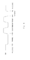
- Fig. 4 shows an example in which preamble period is detected by using five amounts of delay, at timings I to IV.
- the value of the data strobe signal is at high level (1) at the timings I and V, and is at low level (0) at the timings II, III, and IV.
- the adjustment circuit 21 detects that the period between the timing III and the timing IV corresponds to the preamble period.
- the internal clock signal of the processing circuit 7 is output to the DDR SDRAM 9.
- the both circuits operate according to the internal clock signal.
- the DDR SDRAM 9 generates the data strobe signal and the data signal according to the internal clock signal, and then outputs these signals.
- the value of the data strobe signal changes at a timing corresponding to the internal clock signal. Consequently, the adjustment circuit 21 can detect the phase relationship between the data strobe signal and the internal clock signal by detecting the position of the data strobe signal. That is to say, the adjustment circuit 21 can calculate a phase difference between the data strobe signal and the internal clock signal.
- the adjustment circuit 21 stores information indicating a period less than one clock as the phase difference. In the case where the phase difference is equal to or more than one clock, the adjustment circuit 21 outputs information indicating the number of clocks corresponding to the phase difference, as the phase difference information, to the processing circuit 7.
- the strobe value retrieve circuit 23 retrieves the strobe value of the data strobe signal with the valid signal which passes through the valid signal output circuit 22.
- the adjustment circuit 21 repeats issuing the read command and retrieving the strobe value while changing the amount of delay.
- the adjustment circuit 21 can determine the phase relationship between the data strobe signal and the internal clock signal when the data strobe signal is retrieved. As a result, the adjustment circuit 21 obtains the flight time based on the phase relationship.
- the adjustment circuit 21 obtains the phase difference between the internal clock signal and data strobe signal.
- the adjustment circuit 21 notifies the valid signal circuit 22 of the flight time as the amount of delay in order to delay the output of the valid signal in the normal mode.
- the valid signal output circuit 22 delays the timing to output the DQS valid signal output from the processing circuit 7 with the use of the notified amount of delay.
- the valid signal output circuit 22 then outputs the DQS valid signal delayed by the read latency and the flight time as the valid signal to the mask circuit 13.
- the phase difference arises at the time when the data value retrieved at the timing of the data strobe signal is transferred to the internal clock.
- the phase difference can also be calculated by obtaining the phase relationship between the data strobe signal and internal clock signal.
- the adjustment circuit 21 delays outputting the data value output from the flip-flop 15 based on the phase relationship between the data strobe signal and the internal clock signal. Specifically, the adjustment circuit 21 notifies the variable delay circuit 16 of the amount of delay for the data value calculated based on the phase relationship.
- the variable delay circuit 16 delays outputting the data value output from the flip-flop 15 by the notified amount of delay for the data value, and outputs it to the flip-flop 71. Therefore, the flip-flop 71 can reliably retrieve the data value according to the internal clock signal.
- the adjustment circuit 21 and the variable delay circuit 16 performs control so that the proper amount of delay is added to the data value in order to prevent the occurrence of racing. Then, the data value can be reliably transferred to the internal clock,
- Fig. 5 is a timing chart showing signal values obtained after the read command is issued in the normal mode. Symbols "A” to “H” in Fig. 5 correspond to symbols “A” to “H” indicating the signals in Fig. 2 .
- the DDR SDRAM is also referred to as DRAM.
- signals denoted by A to H are referred to as signals A to H, respectively.
- the internal clock signal is shown in the first line and in the second line from the bottom in Fig. 5 .
- the data signal output from DDR SDRAM 9 is shown in the second line.
- the data signal is a signal delayed by the read latency and the flight time to the DDR SDRAM 9.
- the flight time is a sum of a flight time from the issuance of the command by the buffer 26 to the DDR SDRAM 9 and a flight time from the DDR SDRAM 9 to the buffer 11.
- the buffer 11 receives a data signal (signal A) which is delayed by the read latency and the flight time.
- the buffer 12 also receives a data strobe signal (signal B) which is delayed by the read latency and the flight time.
- the valid signal output circuit 22 outputs a valid signal (signal C) which is obtained by delaying the valid signal output from the processing circuit 7 by the read latency and the flight time.
- the mask circuit 13 outputs a logical AND signal (signal D) of the data strobe signal (signal B) and the valid signal (signal C).
- the delay circuit 14 outputs a signal E whose phase is shifted by 90 degrees with respect to the phase of the signal D.
- the flip-flop 15 outputs a signal F which is obtained by retrieving the signal A in accordance with the signal E.
- the signal E is a signal which is obtained by activating the data strobe signal (signal B) by the valid signal (signal C) delayed by the flight time. This enables the flip-flop 15 to retrieve the data value in consideration of the delay corresponding to the flight time.
- the variable delay circuit 16 delays the signal F by a time corresponding to the amount of delay notified by the adjustment circuit 21, and outputs the delayed signal F as a signal G.
- the variable delay circuit 16 adjusts the timing of outputting the signal G so that the flip-flop 71 can easily retrieve the data value according to the internal clock signal.
- the flip-flop 71 retrieves the data value from the signal G according to the internal clock signal and outputs a signal H.
- the data strobe signal (signal B) is asynchronous with the internal clock signal. Therefore, the signal F which retrieves the data value from the data signal in accordance with the data strobe signal is also asynchronous with the internal clock signal. For this reason, the variable delay circuit 16 delays the signal F to shift the phase so that the flip-flop 71 can easily capture the data value according to the internal clock signal. That is, the delay adjustment circuit 1 adjusts the phase difference that is a shift in the phase relationship between the data strobe signal and the internal clock signal. The adjustment is possible because the delay adjustment circuit 1 (adjustment circuit 21) recognizes the phase difference. In this way, the delay adjustment circuit 1 adjusts the output of the signal F to avoid racing. These adjustment functions eliminate the need for a FIFO, thereby making it possible to transfer data from the adjustment circuit 1 to the processing circuit 7 in the shortest period of time.
- the circuit size can be reduced as compared with the technique of Japanese Unexamined Patent Application Publication No. 2005-276396 .
- the technique writes data to the DDR SDRAM 9, reads the written data, and then determines whether the value of the read data is correct or not. After that, the phase relationship with the processing circuit 7 is detected using the determination result, to thereby estimate the flight time. Therefore, the technique requires a circuit for writing data to the DDR SDRAM 9, a circuit for reading data, and a circuit for comparing data with an expectation value, resulting in an increase in circuit size.
- the circuits of this exemplary embodiment calculate the flight time without using the value of the data signal, which eliminates the need for a circuit for reading data and a circuit for comparing data with expectation value. As a result, the size of the circuits for calculating the flight time can be reduced.
- the processing circuit 7 can make the delay adjustment circuit 1 shift to the adjustment mode, and make the control unit 20 calculate the flight time in a period in which no access is made to the DDR SDRAM 9. Accordingly, the circuit of this exemplary embodiment can perform fine adjustment of the timing by causing the adjustment circuit to operate during not only an initial period but a normal operating period. As the result, the circuit of this exemplary embodiment can deal with a variation in the flight time caused due to the environmental changes during operation. In the technique of Japanese Unexamined Patent Application Publication No. 2005-276396 , for example, a power supply is turned off to restart in the case of adjusting the flight time during operation. In this exemplary embodiment, it is possible to adjust the flight time during operation to adapt to the environmental changes without turning off the power supply of the device.
- the delay adjustment circuit 1 uses the internal clock signal of the processing circuit 7 in the case of calculating the flight time. This enables the delay adjustment circuit 1 to obtain the phase relationship between the internal clock signal and the data strobe signal. Therefore, the delay adjustment circuit 1 can perform control using the phase difference between the internal clock and the data strobe signal so that the internal clock can easily capture the data value obtained from the data signal. That is to say, the delay adjustment circuit 1 controls the amount of delay for the data value of the variable delay circuit 16 based on the flight time. This enables the delay adjustment circuit 1 to transfer the data to the internal clock with the smallest amount of delay.
- the internal clock signal is treated as an asynchronous clock signal, so a FIFO is necessary.
- the FIFO synchronizes a signal having an unknown phase relationship to the internal clock signal. Therefore, an extra amount of delay may occur, or the circuit size may be increased.
- the circuit of this exemplary embodiment requires no FIFO, thereby preventing a delay due to the FIFO and an increase in circuit size.
- the delay adjustment circuit 1 generates the valid signal with the flight time. Specifically, because the delay adjustment circuit 1 recognizes the flight time, and thus can control the timing for the valid signal output circuit 22 to output the valid signal after the read command is issued from the processing circuit 7. More specifically, the delay adjustment circuit 1 can control the valid signal output circuit 22 and the mask circuit 13 in accordance with the timing to input the data strobe signal into the buffer 12. Therefore, the data retrieve unit 10 can reliably retrieve the data strobe signal.
- the semiconductor device incorporating the delay adjustment circuit of this exemplary embodiment can perform the operation to make access to the DDR SDRAM without restriction of the flight time of the mounting board.
- the delay adjustment circuit of this exemplary embodiment enables reduction of the circuit size corresponding to the flight time, compared to related arts, resulting in a reduction in chip size of the semiconductor device. Accordingly, it is possible to reduce the cost.
- the circuit of this exemplary embodiment pulls up the data strobe signal to reliably detect the preamble period. This eliminates the need to set the voltage of the second Vref for distinguishing the high impedance state from the low level, unlike Japanese Unexamined Patent Application Publication No. 2003-223786 , for example. As a result, circuits required for these processing can be eliminated in this exemplary embodiment.
- the memory is not limited to the DDR SDRAM.
- the present invention may also be applied to any memory which outputs the data signal and the data strobe signal in response to the issuance of a read command, like the DDR SDRAM.
- the above exemplary embodiments show an example of one semiconductor device (one chip) on which both the delay adjustment device (delay adjustment circuit) and the processing circuit 7 are mounted.
- the configuration of the semiconductor device is not limited thereto. What kind of functions (circuit) are mounted on one semiconductor device is a design issue, so this invention is a not limited to the above exemplary embodiments.
- circuits as the delay adjustment device
- means to implement the delay adjustment device are not limited to circuits (hardware). It may be implemented by hardware, firmware, software, or combination thereof, for example. A part of functions may also be implemented by programs, for example. Programs which are stored in a storage area may be loaded into a memory (RAM: Random Access Memory) to be executed by a CPU (Central Processing Unit) .
- RAM Random Access Memory
- CPU Central Processing Unit
- the delay adjustment circuit 1 receives the clock signal used by the processing circuit 7 and uses the received clock signal.
- a function hat is realized in a smaller circuit size than in the case of using a FIFO.
- the adjustment circuit 21 may calculate the flight time using the data transfer period.
- the number of toggles during the data transfer period is preliminarily defined, The adjustment circuit 21 may also calculate the flight time using a change in waveform of the data strobe signal detected using the number of the toggles,
- the data retrieve unit 10 may include a flip-flop having a similar function. In this case, the data retrieve unit 10 outputs the data value synchronized with the internal clock signal to the processing circuit 7.
- a delay adjustment device that contributes to downsizing the circuit that adjusts a flight time.
- the delay adjustment device is connected to a memory, and adjusts a timing to retrieve data with a data signal and a data strobe signal output from the memory.
- the delay adjustment device includes a data retrieve unit that receives the data signal and the data strobe signal, and outputs a data value of the data signal in accordance with the data strobe signal; and a control unit that issues a read command to the memory, calculates a flight time, and controls a valid period of the data strobe signal based on the flight time.
Landscapes
- Engineering & Computer Science (AREA)
- Microelectronics & Electronic Packaging (AREA)
- Computer Hardware Design (AREA)
- Dram (AREA)
- Memory System (AREA)
- Information Transfer Systems (AREA)
Applications Claiming Priority (1)
| Application Number | Priority Date | Filing Date | Title |
|---|---|---|---|
| JP2008295065A JP2010122842A (ja) | 2008-11-19 | 2008-11-19 | 遅延調整装置、半導体装置及び遅延調整方法 |
Publications (2)
| Publication Number | Publication Date |
|---|---|
| EP2189986A1 true EP2189986A1 (de) | 2010-05-26 |
| EP2189986B1 EP2189986B1 (de) | 2013-07-17 |
Family
ID=41664583
Family Applications (1)
| Application Number | Title | Priority Date | Filing Date |
|---|---|---|---|
| EP09174000.1A Active EP2189986B1 (de) | 2008-11-19 | 2009-10-26 | Verzögerungseinstellungsvorrichtung, Halbleitervorrichtung und Verzögerungseinstellungsverfahren |
Country Status (5)
| Country | Link |
|---|---|
| US (3) | US8228747B2 (de) |
| EP (1) | EP2189986B1 (de) |
| JP (1) | JP2010122842A (de) |
| KR (1) | KR101120975B1 (de) |
| CN (1) | CN101763890A (de) |
Cited By (1)
| Publication number | Priority date | Publication date | Assignee | Title |
|---|---|---|---|---|
| KR20190108346A (ko) * | 2018-03-14 | 2019-09-24 | 에스케이하이닉스 주식회사 | 입출력 회로 |
Families Citing this family (38)
| Publication number | Priority date | Publication date | Assignee | Title |
|---|---|---|---|---|
| KR100832021B1 (ko) * | 2006-06-29 | 2008-05-26 | 주식회사 하이닉스반도체 | 반도체 메모리 소자 및 그 구동방법 |
| US8587337B1 (en) * | 2009-01-31 | 2013-11-19 | Xilinx, Inc. | Method and apparatus for capturing and synchronizing data |
| JP5577776B2 (ja) * | 2010-03-17 | 2014-08-27 | 株式会社リコー | メモリ制御装置及びマスクタイミング制御方法 |
| KR20110131765A (ko) | 2010-05-31 | 2011-12-07 | 주식회사 하이닉스반도체 | 위상 보정 회로 및 이를 이용한 데이터 정렬 회로 |
| JP5655555B2 (ja) | 2010-12-27 | 2015-01-21 | 富士通セミコンダクター株式会社 | メモリインターフェース回路、メモリインターフェース方法、および電子機器 |
| JP5433593B2 (ja) * | 2011-01-21 | 2014-03-05 | 株式会社東芝 | メモリインターフェイスのタイミング調整回路および方法 |
| JP5708258B2 (ja) * | 2011-05-30 | 2015-04-30 | 富士通セミコンダクター株式会社 | 受信回路、システム装置、及びタイミング調整方法 |
| US8565033B1 (en) * | 2011-05-31 | 2013-10-22 | Altera Corporation | Methods for calibrating memory interface circuitry |
| CN102637155B (zh) * | 2012-01-10 | 2014-11-05 | 江苏中科梦兰电子科技有限公司 | 通过训练加修正配置ddr3中数据选通信号延时的方法 |
| KR101930779B1 (ko) * | 2012-04-04 | 2018-12-20 | 에스케이하이닉스 주식회사 | 반도체 메모리 회로 및 이를 이용한 데이터 처리 시스템 |
| CN102693197B (zh) * | 2012-05-07 | 2015-01-28 | 江苏中科梦兰电子科技有限公司 | 内存控制器读选通使能微调寄存器的最小单元计算方法 |
| JP6273856B2 (ja) | 2014-01-24 | 2018-02-07 | 富士通株式会社 | メモリコントローラ及び情報処理装置 |
| US9368172B2 (en) * | 2014-02-03 | 2016-06-14 | Rambus Inc. | Read strobe gating mechanism |
| US9513388B2 (en) * | 2014-03-12 | 2016-12-06 | Sercel | Method for providing synchronization in a data acquisition system |
| US9652228B2 (en) * | 2014-04-03 | 2017-05-16 | Macronix International Co., Ltd. | Devices and operation methods for configuring data strobe signal in memory device |
| CN104505116B (zh) * | 2014-12-11 | 2018-01-19 | 深圳市国微电子有限公司 | 一种用于高速动态存储器的相位调制电路及相位调制方法 |
| US9286961B1 (en) * | 2015-03-30 | 2016-03-15 | Apple Inc. | Memory controller half-clock delay adjustment |
| WO2017130983A1 (ja) * | 2016-01-25 | 2017-08-03 | アイシン・エィ・ダブリュ株式会社 | メモリコントローラ |
| CN108874686B (zh) * | 2017-05-08 | 2021-08-03 | 龙芯中科技术股份有限公司 | 内存参数调节方法、装置及设备 |
| US10026462B1 (en) * | 2017-05-16 | 2018-07-17 | Micron Technology, Inc. | Apparatuses and methods for providing constant DQS-DQ delay in a memory device |
| KR20190023796A (ko) * | 2017-08-30 | 2019-03-08 | 에스케이하이닉스 주식회사 | 메모리 시스템, 메모리 시스템의 동작 방법 및 메모리 장치 |
| KR102378384B1 (ko) * | 2017-09-11 | 2022-03-24 | 삼성전자주식회사 | 불휘발성 메모리 장치의 동작 방법 및 메모리 컨트롤러의 동작 방법 |
| US10437279B2 (en) | 2017-10-11 | 2019-10-08 | Integrated Device Technology, Inc. | Open loop solution in data buffer and RCD |
| US10082823B1 (en) | 2017-10-11 | 2018-09-25 | Integrated Device Technology, Inc. | Open loop solution in data buffer and RCD |
| US10347347B1 (en) * | 2017-12-18 | 2019-07-09 | Intel Corporation | Link training mechanism by controlling delay in data path |
| US10242723B1 (en) * | 2017-12-19 | 2019-03-26 | Apple Inc. | Method and apparatus for background memory subsystem calibration |
| US10360951B1 (en) * | 2018-01-19 | 2019-07-23 | Micron Technology, Inc. | Internal write adjust for a memory device |
| CN108520764B (zh) * | 2018-04-08 | 2019-05-31 | 长鑫存储技术有限公司 | 双倍速率同步动态随机存储器 |
| KR20190121121A (ko) * | 2018-04-17 | 2019-10-25 | 에스케이하이닉스 주식회사 | 반도체장치 |
| CN110648703B (zh) * | 2018-06-26 | 2021-06-15 | 龙芯中科技术股份有限公司 | 数据采集电路、读数据窗口的控制方法及装置 |
| US10546620B2 (en) * | 2018-06-28 | 2020-01-28 | Micron Technology, Inc. | Data strobe calibration |
| US11061431B2 (en) * | 2018-06-28 | 2021-07-13 | Micron Technology, Inc. | Data strobe multiplexer |
| CN109831208A (zh) * | 2019-01-02 | 2019-05-31 | 晶晨半导体(深圳)有限公司 | 测量方法及装置 |
| US11226752B2 (en) | 2019-03-05 | 2022-01-18 | Apple Inc. | Filtering memory calibration |
| US11139008B2 (en) * | 2020-02-03 | 2021-10-05 | Micron Technology, Inc. | Write leveling |
| US11609868B1 (en) | 2020-12-31 | 2023-03-21 | Waymo Llc | Control calibration timing to avoid memory write blackout period |
| KR20230134388A (ko) * | 2022-03-14 | 2023-09-21 | 에스케이하이닉스 주식회사 | 반도체장치 |
| CN115240731B (zh) * | 2022-08-01 | 2026-03-27 | 长鑫存储技术有限公司 | 延迟锁相环电路的控制电路及存储器 |
Citations (5)
| Publication number | Priority date | Publication date | Assignee | Title |
|---|---|---|---|---|
| US6600681B1 (en) * | 2002-06-10 | 2003-07-29 | Lsi Logic Corporation | Method and apparatus for calibrating DQS qualification in a memory controller |
| JP2003223786A (ja) | 2001-09-14 | 2003-08-08 | Sun Microsyst Inc | データストローブ受信機 |
| US6646929B1 (en) * | 2001-12-05 | 2003-11-11 | Lsi Logic Corporation | Methods and structure for read data synchronization with minimal latency |
| JP2005276396A (ja) | 2004-03-26 | 2005-10-06 | Nec Corp | メモリインターフェイス制御回路 |
| JP2008103013A (ja) | 2006-10-18 | 2008-05-01 | Nec Electronics Corp | メモリリード制御回路およびその制御方法 |
Family Cites Families (8)
| Publication number | Priority date | Publication date | Assignee | Title |
|---|---|---|---|---|
| JP3445476B2 (ja) | 1997-10-02 | 2003-09-08 | 株式会社東芝 | 半導体メモリシステム |
| US6456544B1 (en) * | 2001-03-30 | 2002-09-24 | Intel Corporation | Selective forwarding of a strobe based on a predetermined delay following a memory read command |
| JP5013394B2 (ja) * | 2005-09-13 | 2012-08-29 | ルネサスエレクトロニクス株式会社 | 半導体集積回路装置 |
| JP5157194B2 (ja) * | 2006-02-28 | 2013-03-06 | 富士通セミコンダクター株式会社 | データ取込み回路、データ取込みシステム、およびデータ取込み回路の制御方法 |
| JP5023539B2 (ja) * | 2006-04-11 | 2012-09-12 | 富士通セミコンダクター株式会社 | 半導体装置及び信号処理方法 |
| JP4921888B2 (ja) * | 2006-08-22 | 2012-04-25 | ルネサスエレクトロニクス株式会社 | インターフェース回路 |
| JP2008071018A (ja) * | 2006-09-13 | 2008-03-27 | Matsushita Electric Ind Co Ltd | メモリインターフェース回路 |
| JP2010108217A (ja) * | 2008-10-30 | 2010-05-13 | Nec Electronics Corp | メモリインターフェース及びメモリインターフェースの動作方法 |
-
2008
- 2008-11-19 JP JP2008295065A patent/JP2010122842A/ja active Pending
-
2009
- 2009-10-26 EP EP09174000.1A patent/EP2189986B1/de active Active
- 2009-11-02 US US12/588,909 patent/US8228747B2/en active Active
- 2009-11-18 KR KR1020090111632A patent/KR101120975B1/ko not_active Expired - Fee Related
- 2009-11-19 CN CN200910222839A patent/CN101763890A/zh active Pending
-
2012
- 2012-03-06 US US13/413,522 patent/US20120163104A1/en not_active Abandoned
-
2013
- 2013-08-15 US US13/967,540 patent/US20130329504A1/en not_active Abandoned
Patent Citations (5)
| Publication number | Priority date | Publication date | Assignee | Title |
|---|---|---|---|---|
| JP2003223786A (ja) | 2001-09-14 | 2003-08-08 | Sun Microsyst Inc | データストローブ受信機 |
| US6646929B1 (en) * | 2001-12-05 | 2003-11-11 | Lsi Logic Corporation | Methods and structure for read data synchronization with minimal latency |
| US6600681B1 (en) * | 2002-06-10 | 2003-07-29 | Lsi Logic Corporation | Method and apparatus for calibrating DQS qualification in a memory controller |
| JP2005276396A (ja) | 2004-03-26 | 2005-10-06 | Nec Corp | メモリインターフェイス制御回路 |
| JP2008103013A (ja) | 2006-10-18 | 2008-05-01 | Nec Electronics Corp | メモリリード制御回路およびその制御方法 |
Cited By (1)
| Publication number | Priority date | Publication date | Assignee | Title |
|---|---|---|---|---|
| KR20190108346A (ko) * | 2018-03-14 | 2019-09-24 | 에스케이하이닉스 주식회사 | 입출력 회로 |
Also Published As
| Publication number | Publication date |
|---|---|
| JP2010122842A (ja) | 2010-06-03 |
| EP2189986B1 (de) | 2013-07-17 |
| US20120163104A1 (en) | 2012-06-28 |
| US8228747B2 (en) | 2012-07-24 |
| US20100124131A1 (en) | 2010-05-20 |
| KR20100056407A (ko) | 2010-05-27 |
| CN101763890A (zh) | 2010-06-30 |
| US20130329504A1 (en) | 2013-12-12 |
| KR101120975B1 (ko) | 2012-03-05 |
Similar Documents
| Publication | Publication Date | Title |
|---|---|---|
| US8228747B2 (en) | Delay adjustment device, semiconductor device and delay adjustment method | |
| US6889336B2 (en) | Apparatus for improving output skew for synchronous integrate circuits has delay circuit for generating unique clock signal by applying programmable delay to delayed clock signal | |
| JP4450586B2 (ja) | 半導体集積回路 | |
| KR101532529B1 (ko) | 메모리 시스템 내 기록 타이밍을 교정하기 위한 방법 및 장치 | |
| US7161854B2 (en) | Jitter and skew suppressing delay control apparatus | |
| US20080094918A1 (en) | Memory read control circuit and control method thereof | |
| US7266022B2 (en) | Memory interface control circuit | |
| JP5733126B2 (ja) | メモリインタフェース回路及びタイミング調整方法 | |
| US9105327B2 (en) | Memory controller using a data strobe signal and method of calibrating data strobe signal in a memory controller | |
| KR20060111465A (ko) | 2가지 모드의 데이터 스트로브를 구비한 집적 회로 | |
| KR20120030354A (ko) | 메모리 시스템 내에서 쓰기 레벨링을 위한 시작 값들을 조정하는 방법 | |
| US20150194196A1 (en) | Memory system with high performance and high power efficiency and control method of the same | |
| US20030179611A1 (en) | Method and device for controlling data latch time | |
| US8050119B2 (en) | Data output timing in response to read command based on whether delay locked loop is enabled/disabled in a semiconductor device | |
| JP2013109637A (ja) | メモリインターフェース回路、および、そのメモリインターフェース回路の動作方法 | |
| US20150146477A1 (en) | Semiconductor device | |
| US7791963B2 (en) | Semiconductor memory device and operation method thereof | |
| US9135980B2 (en) | Memory control circuit and method of controlling data reading process of memory module | |
| JP2014102741A (ja) | メモリコントローラ及びメモリコントローラのライトレベリング制御方法 | |
| US8797073B2 (en) | Delay locked loop circuit and integrated circuit including the same | |
| US20090319744A1 (en) | Digital Television, Memory Controller, and Method for Controlling Access of a Memory Device | |
| KR101034036B1 (ko) | 반도체 메모리 테스트 보드, 이를 포함하는 반도체 메모리 테스트 시스템 및 반도체 메모리 테스트 방법 | |
| JP2007334943A (ja) | メモリ制御装置 | |
| US12315595B2 (en) | Write leveling circuit applied to memory, and method and apparatus for controlling the same | |
| JP2002324009A (ja) | メモリ制御方法及びメモリ制御システム |
Legal Events
| Date | Code | Title | Description |
|---|---|---|---|
| PUAI | Public reference made under article 153(3) epc to a published international application that has entered the european phase |
Free format text: ORIGINAL CODE: 0009012 |
|
| AK | Designated contracting states |
Kind code of ref document: A1 Designated state(s): AT BE BG CH CY CZ DE DK EE ES FI FR GB GR HR HU IE IS IT LI LT LU LV MC MK MT NL NO PL PT RO SE SI SK SM TR |
|
| AX | Request for extension of the european patent |
Extension state: AL BA RS |
|
| RAP1 | Party data changed (applicant data changed or rights of an application transferred) |
Owner name: RENESAS ELECTRONICS CORPORATION |
|
| 17P | Request for examination filed |
Effective date: 20101126 |
|
| REG | Reference to a national code |
Ref country code: DE Ref legal event code: R079 Ref document number: 602009017180 Country of ref document: DE Free format text: PREVIOUS MAIN CLASS: G11C0007220000 Ipc: G11C0007100000 |
|
| GRAP | Despatch of communication of intention to grant a patent |
Free format text: ORIGINAL CODE: EPIDOSNIGR1 |
|
| RIC1 | Information provided on ipc code assigned before grant |
Ipc: G11C 11/4076 20060101ALI20130118BHEP Ipc: G11C 7/22 20060101ALI20130118BHEP Ipc: G11C 7/10 20060101AFI20130118BHEP Ipc: G11C 29/02 20060101ALI20130118BHEP |
|
| GRAS | Grant fee paid |
Free format text: ORIGINAL CODE: EPIDOSNIGR3 |
|
| GRAA | (expected) grant |
Free format text: ORIGINAL CODE: 0009210 |
|
| AK | Designated contracting states |
Kind code of ref document: B1 Designated state(s): AT BE BG CH CY CZ DE DK EE ES FI FR GB GR HR HU IE IS IT LI LT LU LV MC MK MT NL NO PL PT RO SE SI SK SM TR |
|
| REG | Reference to a national code |
Ref country code: GB Ref legal event code: FG4D |
|
| REG | Reference to a national code |
Ref country code: CH Ref legal event code: EP |
|
| REG | Reference to a national code |
Ref country code: IE Ref legal event code: FG4D |
|
| REG | Reference to a national code |
Ref country code: AT Ref legal event code: REF Ref document number: 622642 Country of ref document: AT Kind code of ref document: T Effective date: 20130815 |
|
| REG | Reference to a national code |
Ref country code: DE Ref legal event code: R096 Ref document number: 602009017180 Country of ref document: DE Effective date: 20130919 |
|
| REG | Reference to a national code |
Ref country code: AT Ref legal event code: MK05 Ref document number: 622642 Country of ref document: AT Kind code of ref document: T Effective date: 20130717 |
|
| REG | Reference to a national code |
Ref country code: NL Ref legal event code: VDEP Effective date: 20130717 |
|
| REG | Reference to a national code |
Ref country code: LT Ref legal event code: MG4D |
|
| PG25 | Lapsed in a contracting state [announced via postgrant information from national office to epo] |
Ref country code: LT Free format text: LAPSE BECAUSE OF FAILURE TO SUBMIT A TRANSLATION OF THE DESCRIPTION OR TO PAY THE FEE WITHIN THE PRESCRIBED TIME-LIMIT Effective date: 20130717 Ref country code: NO Free format text: LAPSE BECAUSE OF FAILURE TO SUBMIT A TRANSLATION OF THE DESCRIPTION OR TO PAY THE FEE WITHIN THE PRESCRIBED TIME-LIMIT Effective date: 20131017 Ref country code: SE Free format text: LAPSE BECAUSE OF FAILURE TO SUBMIT A TRANSLATION OF THE DESCRIPTION OR TO PAY THE FEE WITHIN THE PRESCRIBED TIME-LIMIT Effective date: 20130717 Ref country code: PT Free format text: LAPSE BECAUSE OF FAILURE TO SUBMIT A TRANSLATION OF THE DESCRIPTION OR TO PAY THE FEE WITHIN THE PRESCRIBED TIME-LIMIT Effective date: 20131118 Ref country code: HR Free format text: LAPSE BECAUSE OF FAILURE TO SUBMIT A TRANSLATION OF THE DESCRIPTION OR TO PAY THE FEE WITHIN THE PRESCRIBED TIME-LIMIT Effective date: 20130717 Ref country code: AT Free format text: LAPSE BECAUSE OF FAILURE TO SUBMIT A TRANSLATION OF THE DESCRIPTION OR TO PAY THE FEE WITHIN THE PRESCRIBED TIME-LIMIT Effective date: 20130717 Ref country code: CY Free format text: LAPSE BECAUSE OF FAILURE TO SUBMIT A TRANSLATION OF THE DESCRIPTION OR TO PAY THE FEE WITHIN THE PRESCRIBED TIME-LIMIT Effective date: 20130828 Ref country code: IS Free format text: LAPSE BECAUSE OF FAILURE TO SUBMIT A TRANSLATION OF THE DESCRIPTION OR TO PAY THE FEE WITHIN THE PRESCRIBED TIME-LIMIT Effective date: 20131117 Ref country code: BE Free format text: LAPSE BECAUSE OF FAILURE TO SUBMIT A TRANSLATION OF THE DESCRIPTION OR TO PAY THE FEE WITHIN THE PRESCRIBED TIME-LIMIT Effective date: 20130717 |
|
| PG25 | Lapsed in a contracting state [announced via postgrant information from national office to epo] |
Ref country code: GR Free format text: LAPSE BECAUSE OF FAILURE TO SUBMIT A TRANSLATION OF THE DESCRIPTION OR TO PAY THE FEE WITHIN THE PRESCRIBED TIME-LIMIT Effective date: 20131018 Ref country code: NL Free format text: LAPSE BECAUSE OF FAILURE TO SUBMIT A TRANSLATION OF THE DESCRIPTION OR TO PAY THE FEE WITHIN THE PRESCRIBED TIME-LIMIT Effective date: 20130717 Ref country code: PL Free format text: LAPSE BECAUSE OF FAILURE TO SUBMIT A TRANSLATION OF THE DESCRIPTION OR TO PAY THE FEE WITHIN THE PRESCRIBED TIME-LIMIT Effective date: 20130717 Ref country code: FI Free format text: LAPSE BECAUSE OF FAILURE TO SUBMIT A TRANSLATION OF THE DESCRIPTION OR TO PAY THE FEE WITHIN THE PRESCRIBED TIME-LIMIT Effective date: 20130717 Ref country code: ES Free format text: LAPSE BECAUSE OF FAILURE TO SUBMIT A TRANSLATION OF THE DESCRIPTION OR TO PAY THE FEE WITHIN THE PRESCRIBED TIME-LIMIT Effective date: 20131028 Ref country code: SI Free format text: LAPSE BECAUSE OF FAILURE TO SUBMIT A TRANSLATION OF THE DESCRIPTION OR TO PAY THE FEE WITHIN THE PRESCRIBED TIME-LIMIT Effective date: 20130717 Ref country code: LV Free format text: LAPSE BECAUSE OF FAILURE TO SUBMIT A TRANSLATION OF THE DESCRIPTION OR TO PAY THE FEE WITHIN THE PRESCRIBED TIME-LIMIT Effective date: 20130717 |
|
| PG25 | Lapsed in a contracting state [announced via postgrant information from national office to epo] |
Ref country code: CY Free format text: LAPSE BECAUSE OF FAILURE TO SUBMIT A TRANSLATION OF THE DESCRIPTION OR TO PAY THE FEE WITHIN THE PRESCRIBED TIME-LIMIT Effective date: 20130717 |
|
| PG25 | Lapsed in a contracting state [announced via postgrant information from national office to epo] |
Ref country code: RO Free format text: LAPSE BECAUSE OF FAILURE TO SUBMIT A TRANSLATION OF THE DESCRIPTION OR TO PAY THE FEE WITHIN THE PRESCRIBED TIME-LIMIT Effective date: 20130717 Ref country code: DK Free format text: LAPSE BECAUSE OF FAILURE TO SUBMIT A TRANSLATION OF THE DESCRIPTION OR TO PAY THE FEE WITHIN THE PRESCRIBED TIME-LIMIT Effective date: 20130717 Ref country code: SK Free format text: LAPSE BECAUSE OF FAILURE TO SUBMIT A TRANSLATION OF THE DESCRIPTION OR TO PAY THE FEE WITHIN THE PRESCRIBED TIME-LIMIT Effective date: 20130717 Ref country code: CZ Free format text: LAPSE BECAUSE OF FAILURE TO SUBMIT A TRANSLATION OF THE DESCRIPTION OR TO PAY THE FEE WITHIN THE PRESCRIBED TIME-LIMIT Effective date: 20130717 Ref country code: EE Free format text: LAPSE BECAUSE OF FAILURE TO SUBMIT A TRANSLATION OF THE DESCRIPTION OR TO PAY THE FEE WITHIN THE PRESCRIBED TIME-LIMIT Effective date: 20130717 |
|
| PLBE | No opposition filed within time limit |
Free format text: ORIGINAL CODE: 0009261 |
|
| STAA | Information on the status of an ep patent application or granted ep patent |
Free format text: STATUS: NO OPPOSITION FILED WITHIN TIME LIMIT |
|
| PG25 | Lapsed in a contracting state [announced via postgrant information from national office to epo] |
Ref country code: IT Free format text: LAPSE BECAUSE OF FAILURE TO SUBMIT A TRANSLATION OF THE DESCRIPTION OR TO PAY THE FEE WITHIN THE PRESCRIBED TIME-LIMIT Effective date: 20130717 Ref country code: MC Free format text: LAPSE BECAUSE OF FAILURE TO SUBMIT A TRANSLATION OF THE DESCRIPTION OR TO PAY THE FEE WITHIN THE PRESCRIBED TIME-LIMIT Effective date: 20130717 |
|
| REG | Reference to a national code |
Ref country code: CH Ref legal event code: PL |
|
| 26N | No opposition filed |
Effective date: 20140422 |
|
| GBPC | Gb: european patent ceased through non-payment of renewal fee |
Effective date: 20131026 |
|
| REG | Reference to a national code |
Ref country code: IE Ref legal event code: MM4A |
|
| PG25 | Lapsed in a contracting state [announced via postgrant information from national office to epo] |
Ref country code: LI Free format text: LAPSE BECAUSE OF NON-PAYMENT OF DUE FEES Effective date: 20131031 Ref country code: CH Free format text: LAPSE BECAUSE OF NON-PAYMENT OF DUE FEES Effective date: 20131031 Ref country code: GB Free format text: LAPSE BECAUSE OF NON-PAYMENT OF DUE FEES Effective date: 20131026 |
|
| REG | Reference to a national code |
Ref country code: DE Ref legal event code: R097 Ref document number: 602009017180 Country of ref document: DE Effective date: 20140422 |
|
| REG | Reference to a national code |
Ref country code: FR Ref legal event code: ST Effective date: 20140630 |
|
| PG25 | Lapsed in a contracting state [announced via postgrant information from national office to epo] |
Ref country code: FR Free format text: LAPSE BECAUSE OF NON-PAYMENT OF DUE FEES Effective date: 20131031 |
|
| PG25 | Lapsed in a contracting state [announced via postgrant information from national office to epo] |
Ref country code: IE Free format text: LAPSE BECAUSE OF NON-PAYMENT OF DUE FEES Effective date: 20131026 |
|
| PG25 | Lapsed in a contracting state [announced via postgrant information from national office to epo] |
Ref country code: SM Free format text: LAPSE BECAUSE OF FAILURE TO SUBMIT A TRANSLATION OF THE DESCRIPTION OR TO PAY THE FEE WITHIN THE PRESCRIBED TIME-LIMIT Effective date: 20130717 |
|
| PG25 | Lapsed in a contracting state [announced via postgrant information from national office to epo] |
Ref country code: TR Free format text: LAPSE BECAUSE OF FAILURE TO SUBMIT A TRANSLATION OF THE DESCRIPTION OR TO PAY THE FEE WITHIN THE PRESCRIBED TIME-LIMIT Effective date: 20130717 |
|
| PG25 | Lapsed in a contracting state [announced via postgrant information from national office to epo] |
Ref country code: MK Free format text: LAPSE BECAUSE OF FAILURE TO SUBMIT A TRANSLATION OF THE DESCRIPTION OR TO PAY THE FEE WITHIN THE PRESCRIBED TIME-LIMIT Effective date: 20130717 Ref country code: LU Free format text: LAPSE BECAUSE OF NON-PAYMENT OF DUE FEES Effective date: 20131026 Ref country code: HU Free format text: LAPSE BECAUSE OF FAILURE TO SUBMIT A TRANSLATION OF THE DESCRIPTION OR TO PAY THE FEE WITHIN THE PRESCRIBED TIME-LIMIT; INVALID AB INITIO Effective date: 20091026 Ref country code: BG Free format text: LAPSE BECAUSE OF FAILURE TO SUBMIT A TRANSLATION OF THE DESCRIPTION OR TO PAY THE FEE WITHIN THE PRESCRIBED TIME-LIMIT Effective date: 20130717 |
|
| PG25 | Lapsed in a contracting state [announced via postgrant information from national office to epo] |
Ref country code: MT Free format text: LAPSE BECAUSE OF FAILURE TO SUBMIT A TRANSLATION OF THE DESCRIPTION OR TO PAY THE FEE WITHIN THE PRESCRIBED TIME-LIMIT Effective date: 20130717 |
|
| REG | Reference to a national code |
Ref country code: DE Ref legal event code: R082 Ref document number: 602009017180 Country of ref document: DE Representative=s name: BETTEN & RESCH PATENT- UND RECHTSANWAELTE PART, DE Ref country code: DE Ref legal event code: R081 Ref document number: 602009017180 Country of ref document: DE Owner name: RENESAS ELECTRONICS CORPORATION, JP Free format text: FORMER OWNER: RENESAS ELECTRONICS CORPORATION, KAWASAKI, KANAGAWA, JP |
|
| PGFP | Annual fee paid to national office [announced via postgrant information from national office to epo] |
Ref country code: DE Payment date: 20251028 Year of fee payment: 17 |