US11226752B2 - Filtering memory calibration - Google Patents

Filtering memory calibration Download PDF

Info

Publication number
US11226752B2
US11226752B2 US16/293,398 US201916293398A US11226752B2 US 11226752 B2 US11226752 B2 US 11226752B2 US 201916293398 A US201916293398 A US 201916293398A US 11226752 B2 US11226752 B2 US 11226752B2
Authority
US
United States
Prior art keywords
memory
state
timer
calibration
indication
Prior art date
Legal status (The legal status is an assumption and is not a legal conclusion. Google has not performed a legal analysis and makes no representation as to the accuracy of the status listed.)
Active, expires
Application number
US16/293,398
Other versions
US20200285406A1 (en
Inventor
Rakesh L. Notani
Robert E. Jeter
Suhas Kumar Suvarna Ramesh
Naveen Kumar Korada
Mohammad RIZWAN
Alma L. Juarez Dominguez
John H. Kelm
Matthew R. Johnson
Current Assignee (The listed assignees may be inaccurate. Google has not performed a legal analysis and makes no representation or warranty as to the accuracy of the list.)
Apple Inc
Original Assignee
Apple Inc
Priority date (The priority date is an assumption and is not a legal conclusion. Google has not performed a legal analysis and makes no representation as to the accuracy of the date listed.)
Filing date
Publication date
Application filed by Apple Inc filed Critical Apple Inc
Priority to US16/293,398 priority Critical patent/US11226752B2/en
Assigned to APPLE INC. reassignment APPLE INC. ASSIGNMENT OF ASSIGNORS INTEREST (SEE DOCUMENT FOR DETAILS). Assignors: JOHNSON, MATTHEW R., JUAREZ DOMINGUEZ, ALMA L., KELM, John H., JETER, ROBERT E., KORADA, NAVEEN KUMAR, Notani, Rakesh L., RIZWAN, Mohammad, SUVARNA RAMESH, SUHAS KUMAR
Publication of US20200285406A1 publication Critical patent/US20200285406A1/en
Application granted granted Critical
Publication of US11226752B2 publication Critical patent/US11226752B2/en
Active legal-status Critical Current
Adjusted expiration legal-status Critical

Links

Images

Classifications

    • GPHYSICS
    • G06COMPUTING; CALCULATING OR COUNTING
    • G06FELECTRIC DIGITAL DATA PROCESSING
    • G06F3/00Input arrangements for transferring data to be processed into a form capable of being handled by the computer; Output arrangements for transferring data from processing unit to output unit, e.g. interface arrangements
    • G06F3/06Digital input from, or digital output to, record carriers, e.g. RAID, emulated record carriers or networked record carriers
    • G06F3/0601Interfaces specially adapted for storage systems
    • G06F3/0628Interfaces specially adapted for storage systems making use of a particular technique
    • G06F3/0629Configuration or reconfiguration of storage systems
    • G06F3/0634Configuration or reconfiguration of storage systems by changing the state or mode of one or more devices
    • GPHYSICS
    • G11INFORMATION STORAGE
    • G11CSTATIC STORES
    • G11C11/00Digital stores characterised by the use of particular electric or magnetic storage elements; Storage elements therefor
    • G11C11/21Digital stores characterised by the use of particular electric or magnetic storage elements; Storage elements therefor using electric elements
    • G11C11/34Digital stores characterised by the use of particular electric or magnetic storage elements; Storage elements therefor using electric elements using semiconductor devices
    • G11C11/40Digital stores characterised by the use of particular electric or magnetic storage elements; Storage elements therefor using electric elements using semiconductor devices using transistors
    • G11C11/401Digital stores characterised by the use of particular electric or magnetic storage elements; Storage elements therefor using electric elements using semiconductor devices using transistors forming cells needing refreshing or charge regeneration, i.e. dynamic cells
    • G11C11/4063Auxiliary circuits, e.g. for addressing, decoding, driving, writing, sensing or timing
    • G11C11/407Auxiliary circuits, e.g. for addressing, decoding, driving, writing, sensing or timing for memory cells of the field-effect type
    • G11C11/4072Circuits for initialization, powering up or down, clearing memory or presetting
    • GPHYSICS
    • G06COMPUTING; CALCULATING OR COUNTING
    • G06FELECTRIC DIGITAL DATA PROCESSING
    • G06F3/00Input arrangements for transferring data to be processed into a form capable of being handled by the computer; Output arrangements for transferring data from processing unit to output unit, e.g. interface arrangements
    • G06F3/06Digital input from, or digital output to, record carriers, e.g. RAID, emulated record carriers or networked record carriers
    • G06F3/0601Interfaces specially adapted for storage systems
    • G06F3/0602Interfaces specially adapted for storage systems specifically adapted to achieve a particular effect
    • G06F3/0604Improving or facilitating administration, e.g. storage management
    • GPHYSICS
    • G06COMPUTING; CALCULATING OR COUNTING
    • G06FELECTRIC DIGITAL DATA PROCESSING
    • G06F3/00Input arrangements for transferring data to be processed into a form capable of being handled by the computer; Output arrangements for transferring data from processing unit to output unit, e.g. interface arrangements
    • G06F3/06Digital input from, or digital output to, record carriers, e.g. RAID, emulated record carriers or networked record carriers
    • G06F3/0601Interfaces specially adapted for storage systems
    • G06F3/0668Interfaces specially adapted for storage systems adopting a particular infrastructure
    • G06F3/0671In-line storage system
    • G06F3/0673Single storage device
    • GPHYSICS
    • G11INFORMATION STORAGE
    • G11CSTATIC STORES
    • G11C11/00Digital stores characterised by the use of particular electric or magnetic storage elements; Storage elements therefor
    • G11C11/21Digital stores characterised by the use of particular electric or magnetic storage elements; Storage elements therefor using electric elements
    • G11C11/34Digital stores characterised by the use of particular electric or magnetic storage elements; Storage elements therefor using electric elements using semiconductor devices
    • G11C11/40Digital stores characterised by the use of particular electric or magnetic storage elements; Storage elements therefor using electric elements using semiconductor devices using transistors
    • G11C11/401Digital stores characterised by the use of particular electric or magnetic storage elements; Storage elements therefor using electric elements using semiconductor devices using transistors forming cells needing refreshing or charge regeneration, i.e. dynamic cells
    • G11C11/4063Auxiliary circuits, e.g. for addressing, decoding, driving, writing, sensing or timing
    • G11C11/407Auxiliary circuits, e.g. for addressing, decoding, driving, writing, sensing or timing for memory cells of the field-effect type
    • G11C11/4074Power supply or voltage generation circuits, e.g. bias voltage generators, substrate voltage generators, back-up power, power control circuits
    • GPHYSICS
    • G11INFORMATION STORAGE
    • G11CSTATIC STORES
    • G11C11/00Digital stores characterised by the use of particular electric or magnetic storage elements; Storage elements therefor
    • G11C11/21Digital stores characterised by the use of particular electric or magnetic storage elements; Storage elements therefor using electric elements
    • G11C11/34Digital stores characterised by the use of particular electric or magnetic storage elements; Storage elements therefor using electric elements using semiconductor devices
    • G11C11/40Digital stores characterised by the use of particular electric or magnetic storage elements; Storage elements therefor using electric elements using semiconductor devices using transistors
    • G11C11/401Digital stores characterised by the use of particular electric or magnetic storage elements; Storage elements therefor using electric elements using semiconductor devices using transistors forming cells needing refreshing or charge regeneration, i.e. dynamic cells
    • G11C11/4063Auxiliary circuits, e.g. for addressing, decoding, driving, writing, sensing or timing
    • G11C11/407Auxiliary circuits, e.g. for addressing, decoding, driving, writing, sensing or timing for memory cells of the field-effect type
    • G11C11/4076Timing circuits
    • GPHYSICS
    • G11INFORMATION STORAGE
    • G11CSTATIC STORES
    • G11C11/00Digital stores characterised by the use of particular electric or magnetic storage elements; Storage elements therefor
    • G11C11/21Digital stores characterised by the use of particular electric or magnetic storage elements; Storage elements therefor using electric elements
    • G11C11/34Digital stores characterised by the use of particular electric or magnetic storage elements; Storage elements therefor using electric elements using semiconductor devices
    • G11C11/40Digital stores characterised by the use of particular electric or magnetic storage elements; Storage elements therefor using electric elements using semiconductor devices using transistors
    • G11C11/401Digital stores characterised by the use of particular electric or magnetic storage elements; Storage elements therefor using electric elements using semiconductor devices using transistors forming cells needing refreshing or charge regeneration, i.e. dynamic cells
    • G11C11/4063Auxiliary circuits, e.g. for addressing, decoding, driving, writing, sensing or timing
    • G11C11/407Auxiliary circuits, e.g. for addressing, decoding, driving, writing, sensing or timing for memory cells of the field-effect type
    • G11C11/409Read-write [R-W] circuits 
    • G11C11/4093Input/output [I/O] data interface arrangements, e.g. data buffers
    • GPHYSICS
    • G11INFORMATION STORAGE
    • G11CSTATIC STORES
    • G11C7/00Arrangements for writing information into, or reading information out from, a digital store
    • G11C7/22Read-write [R-W] timing or clocking circuits; Read-write [R-W] control signal generators or management 
    • GPHYSICS
    • G11INFORMATION STORAGE
    • G11CSTATIC STORES
    • G11C2207/00Indexing scheme relating to arrangements for writing information into, or reading information out from, a digital store
    • G11C2207/22Control and timing of internal memory operations
    • G11C2207/2254Calibration
    • GPHYSICS
    • G11INFORMATION STORAGE
    • G11CSTATIC STORES
    • G11C5/00Details of stores covered by group G11C11/00
    • G11C5/14Power supply arrangements, e.g. power down, chip selection or deselection, layout of wirings or power grids, or multiple supply levels
    • GPHYSICS
    • G11INFORMATION STORAGE
    • G11CSTATIC STORES
    • G11C7/00Arrangements for writing information into, or reading information out from, a digital store
    • G11C7/10Input/output [I/O] data interface arrangements, e.g. I/O data control circuits, I/O data buffers
    • G11C7/1048Data bus control circuits, e.g. precharging, presetting, equalising
    • GPHYSICS
    • G11INFORMATION STORAGE
    • G11CSTATIC STORES
    • G11C7/00Arrangements for writing information into, or reading information out from, a digital store
    • G11C7/20Memory cell initialisation circuits, e.g. when powering up or down, memory clear, latent image memory

Definitions

  • Embodiments described herein relate to the field of computing systems and, more particularly, to efficiently calibrating memory signals.
  • a variety of computing systems include a processor and a memory.
  • the processor generates access requests for instructions and application data while processing one or more software applications.
  • the processor checks a hierarchy of local cache memories and, if not found, the processor issues requests for the desired instructions and data to system memory.
  • the system memory is typically implemented as one of a variety of types of off-chip dynamic random access memory (DRAM).
  • DRAM off-chip dynamic random access memory
  • Accessing data in the system memory is a complex process with many behind-the-scenes steps performed by the memory controller.
  • the memory controller determines when to change from sending read operations to sending write operations, and thus, direct the off-chip data bus to turn around and drive data in the opposite direction.
  • the memory controller also schedules requests and responses based on a variety of criteria, each with a given priority.
  • the internal processes of the memory of the DRAM is complex with activation/open transactions, column access transactions, read access transactions, write access transactions, and precharge/close transactions.
  • the memory controller initiates periodic calibration of the DRAM.
  • These calibration processes are needed to fine-tune various parameters to optimize performance and functionality of the DRAM at a target clock frequency.
  • Examples of the periodic calibration processes are ZQ calibration that tunes the on-die termination (ODT) resistances, write leveling calibration, data strobe signal (DQS) gating calibration, write data DQS calibration, read data DQS calibration, write data bit delay calibration to determine the additional delay for each output data bit, read data bit delay calibration to determine the additional delay for each input data bit, and so on.
  • ODT on-die termination
  • DQS data strobe signal
  • computing systems typically include control logic, such as a power management unit, for determining one or more power-performance states (p-states) for the different functional units in the system.
  • p-states power-performance states
  • Each of the multiple p-states includes a power supply voltage and an operational clock frequency.
  • Clock generating circuitry generates different clock signals at the one or more specified different frequencies, whereas a power distribution network provides the one or more specified different power supply voltages.
  • the power management unit changes the p-states of the functional units including the memory.
  • calibration of the DRAM is dependent on the operational clock frequency. Each time the operational clock frequency is changed, one or more of the various calibration processes are repeated. The calibration processes also consumes power. As the frequency of the changes to the p-states increase, the amount of power consumed by the calibration processes also increase.
  • a computing system includes at least one processor, a memory and a power manager.
  • the processor generates memory requests and the memory stores data requested by the processor.
  • the power manager generates and sends updated power-performance states (p-states) to the processor and the memory.
  • a memory controller for the memory maintains a first timer corresponding to a first p-state of the multiple p-states.
  • the memory controller maintains a respective timer for two or more p-states of the multiple p-states.
  • the memory controller maintains a respective timer for each of the multiple p-states.
  • Each of the multiple p-states includes operating parameters such as a power supply voltage and an operational clock frequency.
  • the memory controller initializes the first timer to indicate a duration for skipping memory calibration.
  • a duration for skipping memory calibration refers to a duration during which memory calibration is not to be performed.
  • the memory controller selects a duration greater than a time period between updates of the p-states from the power manager.
  • the memory controller continues to update the first timer while transferring data with the memory using operating parameters of the first p-state.
  • the memory controller decrements the timer during each clock cycle from a first value to a second value while transferring data with the memory using operating parameters of the first p-state.
  • the first value is a count of clock cycles equivalent to the desired duration for skipping memory calibration and the second value is zero.
  • the memory controller increments the timer during each clock cycle from the first value to the second value while transferring data with the memory using operating parameters of the first p-state.
  • the first value is zero and the second value is the count of clock cycles equivalent to the desired duration for skipping memory calibration.
  • the memory controller continues to update a second timer while transferring data with the memory using operating parameters of the second p-state.
  • the memory controller prevents updates of the first timer. For example, the memory controller no longer decrements or increments the first timer.
  • the memory controller When the memory controller receives an indication to transition the memory from the first p-state to the second p-state, the memory controller inspects the second timer of the second p-state. If the second timer has not expired, then the memory controller prevents calibration of the memory. Therefore, memory is not calibrated for each change of the operating parameters associated with p-state changes.
  • the memory controller conveys an indication to one or more agents that a latency for the transition to the second p-state for the memory does not include an added latency for memory calibration. Therefore, the agents are able to adjust a number of requests to store in queues while waiting for the p-state change to complete.
  • the memory controller performs one or more memory calibration processes. When the memory calibration processes complete, the memory controller resets the second timer to the desired duration for skipping memory calibration. If the memory continues to use the operating parameters of the second p-state, then the memory controller continues to update the second timer such as incrementing or decrementing the second timer.
  • FIG. 1 is a block diagram of one embodiment of sequences for handling memory calibration with transitions of power-performance states.
  • FIG. 2 is a block diagram of one embodiment of a computing system.
  • FIG. 3 is a flow diagram of one embodiment of a method for efficiently handling memory calibration with transitions of power-performance states.
  • FIG. 4 is a flow diagram of one embodiment of a method for efficiently handling memory calibration with transitions of power-performance states.
  • FIG. 5 is a flow diagram of one embodiment of a method for efficiently handling memory calibration with transitions of power-performance states.
  • FIG. 6 is a flow diagram of one embodiment of a method for efficiently handling memory calibration with transitions of power-performance states.
  • FIG. 7 is a flow diagram of one embodiment of a method for efficiently handling memory calibration with transitions of power-performance states.
  • FIG. 8 is a block diagram of one embodiment of a computing system.
  • FIG. 9 is a block diagram of one embodiment of a system.
  • circuits, or other components may be described as “configured to” perform a task or tasks.
  • “configured to” is a broad recitation of structure generally meaning “having circuitry that” performs the task or tasks during operation.
  • the unit/circuit/component can be configured to perform the task even when the unit/circuit/component is not currently on.
  • the circuitry that forms the structure corresponding to “configured to” may include hardware circuits.
  • various units/circuits/components may be described as performing a task or tasks, for convenience in the description.
  • sequence 100 includes multiple points in time from time t 1 to time t 12 indicating when performance state changes occur.
  • the performance state changes are equivalent to changes in the operating parameters of power-performance states (p-states).
  • Each of the multiple p-states includes operating parameters such as a power supply voltage and an operational clock frequency.
  • Clock generating circuitry generates different clock signals at the one or more specified different frequencies, whereas a power distribution network provides the one or more specified different power supply voltages.
  • a power management unit changes the p-states of functional units in a computing system including a memory.
  • the memory is system memory, which is typically implemented as one of a variety of types of off-chip dynamic random access memory (DRAM).
  • DRAM off-chip dynamic random access memory
  • a power management unit which is also referred to as a power manager, sends an indication of a p-state change to the memory.
  • control logic in one or more of the memory controller and the memory changes the operating parameters of the memory to the operating parameters of the new p-state.
  • control logic in one or more of the memory controller and the memory perform one or more memory calibration processes. Some of the memory calibration processes are performed simultaneously as the operating parameter are changing. Other memory calibrations processes wait until the changes for the operating parameters complete before beginning.
  • Examples of the periodic calibration processes are ZQ calibration that tunes the on-die termination (ODT) resistances, write leveling calibration, data strobe signal (DQS) gating calibration, write data DQS calibration, read data DQS calibration, write data bit delay calibration to determine the additional delay for each output data bit, read data bit delay calibration to determine the additional delay for each input data bit, and so on.
  • ODT on-die termination
  • DQS data strobe signal
  • the power manager changes p-states for the computing system for reducing power consumption when possible, the memory calibration processes also consume power. As shown, the power manager sends performance state changes to the memory at times t 3 , t 5 , t 7 , t 9 and t 11 . At each of these points in time, one or more memory calibration processes are also performed, and accordingly, power is consumed. Reducing the frequency of performing the memory calibration processes also further reduces power consumption of the computing system.
  • sequence 150 includes multiple points in time from time t 13 to time t 24 indicating when performance state changes occur and when memory calibrations processes are prevented.
  • a power manager sends an indication of a p-state change to the memory.
  • one or more memory calibration processes are also performed, and accordingly, power is consumed.
  • the power manager again sends an indication of a p-state change to the memory.
  • each of the memory calibration processes is prevented from being performed. Therefore, no additional power is consumed for the memory calibration processes.
  • the power manager sends performance state changes to the memory.
  • logic in the memory controller prevents performing each of the memory calibration processes.
  • the power consumption for sequence 150 is less than the power consumption for sequence 100 .
  • Adding logic for determining when to prevent performing memory calibration processes for each performance state change reduces the system's power consumption while supporting frequent p-state changes.
  • a power manager 210 transfers information between multiple components such as processors 220 and 222 , memory controller 230 and memory 260 .
  • the processors 220 and 222 transfer messages and data to one another and power manager 210 .
  • the processors 220 and 222 transfer messages and data to memory 260 via the memory controller 230 .
  • the components of computing system 200 utilize a communication fabric (not shown) for the transferring of information. Although only two processors are shown, in other embodiments, another number of processors are in the computing system 200 .
  • the computing system 200 includes other components such as an input/output (I/O) interface and other types of processing units such as a multimedia engine, a camera and so on.
  • I/O input/output
  • the power manager 210 receives feedback information from the other components of the computing system 200 .
  • the power manager 210 receives measurements from one or more on-die temperature sensors and one or more power supply sensors, which are not shown for ease of illustration.
  • the power manager receives an indication of an activity level of the other components.
  • one or more of the memory controller 230 and the processors 220 and 222 send an indication of an activity level based on a predetermined range.
  • the components send a weighted sum of sampled signals.
  • one or more of clock enable signals routed to local clock distribution blocks, cache access hit/miss status, bus driver enable signals and so on are examples of signals chosen to be sampled.
  • the power manager 210 processes the received feedback information and adjusts the operating parameters of one or more of the components of computing system 200 . For example, the power manager 210 sends an updated p-state to one or more of the components.
  • Each of the processors 220 and 222 include one or more processor cores and use local storage such as a cache memory subsystem. When the processor cores do not find requested data in local storage, the processor cores generate memory requests and send them to the memory 260 via the memory controller 230 .
  • Examples of the processors 220 and 222 are a general-purpose central processing unit (CPU), a processor with single instruction multiple data (SIMD) cores, such as a graphics processing unit (GPU), a digital signal processor (DSP), and so forth.
  • the memory 260 is implemented as one of a variety of types of off-chip dynamic random access memory (DRAM). When requested data is not stored in the memory 260 , then the memory controller 230 forwards the requests to main memory implemented with one or more of a hard disk drive, a solid-state drive, and so forth.
  • the memory controller 230 includes queues 232 A- 232 B for storing memory requests received from the processors 220 and 222 .
  • one or more of the queues 232 A- 232 B store memory responses received from the memory 260 .
  • the memory responses include requested read data and write acknowledgments.
  • Logic 240 routes the requests and the responses to the appropriate one of the queues 232 A- 232 B.
  • Logic 240 also schedules the requests and responses to be deallocated from the queues 232 A- 232 B based on one of a variety of arbitration schemes.
  • the memory controller 230 also includes calibration logic 256 for initiating and/or performing one or more memory calibration processes for the memory 260 .
  • calibration filter 254 determines when to prevent calibration of the memory 260 .
  • calibration filter 254 maintains the timers 250 A- 250 B, and prevents memory calibration during particular events.
  • the calibration filter 254 maintains a separate timer of the timers 250 A- 250 B for each of the available p-states.
  • the calibration filter 254 initializes the timers 250 A- 250 B to indicate a duration during which memory calibration is not to be performed.
  • the calibration filter 254 selects a duration greater than a time period between updates of the p-states from the power manager 210 .
  • the power manager sends updates of p-states every 50 microseconds to every 20 milliseconds, and the calibration filter 254 initializes the timers 250 A- 250 B with a value of 200 milliseconds.
  • the timers 250 A- 250 B are counters, and the initial value is a count of clock cycles that provides an equivalent duration of time as the selected 200 milliseconds.
  • the calibration filter 254 continues to update a first timer of the timers 250 A- 250 B while the memory controller 230 transfers data with the memory 260 using operating parameters of the first p-state corresponding to the first timer.
  • the calibration filter 254 updates the first timer by decrementing the first timer during each clock cycle from a first value to a second value while the memory 260 uses the operating parameters of the first p-state.
  • the first value is a count of clock cycles equivalent to the desired duration for skipping memory calibration and the second value is zero.
  • a duration for skipping memory calibration refers to a duration during which memory calibration is not to be performed.
  • the calibration filter 254 updates the first timer by incrementing the first timer during each clock cycle from the first value to the second value while the memory 260 uses the operating parameters of the first p-state.
  • the first value is zero and the second value is the count of clock cycles equivalent to the desired duration for skipping memory calibration.
  • the calibration filter 254 continues to update a second timer while the memory 260 uses the operating parameters of the first p-state.
  • the calibration filter 254 prevents updates of the first timer. For example, the calibration filter 254 no longer decrements or increments the first timer.
  • the calibration filter 254 does not update the first timer until the calibration filter 254 receives an indication from the calibration logic 256 that memory calibration eventually completed while the memory 260 uses the operation parameters of the first p-state.
  • the calibration filter 254 inspects the second timer of the second p-state. If the second timer has not expired, then the calibration filter 254 prevents calibration of the memory 260 . For example, the calibration filter 254 sends an indication to the calibration logic 256 to halt any of the memory calibration processes. Therefore, the memory 260 is not calibrated for each change of the operating parameters associated with p-state changes.
  • the memory controller 230 conveys an indication to one or more of the processors 220 and 222 that a latency for the transition to the second p-state for the memory 260 does not include an added latency for memory calibration.
  • one or more of the processors 220 and 222 are able to adjust a number of requests to store in queues while waiting for the p-state change to complete for the memory 260 . For example, when one or more of the processors 220 and 222 execute real-time applications, the knowledge of the reduced latency improves performance.
  • clock sources such as phase lock loops (PLLs), interrupt controllers, and so forth are not shown in FIG. 2 for ease of illustration.
  • PLLs phase lock loops
  • the number of components of the computing system 200 (and the number of subcomponents for those shown in FIG. 2 , such as within the memory controller 230 ) may vary from embodiment to embodiment.
  • the functionality of the subcomponents in the memory controller 230 is implemented with hardware, such as circuitry, by software, or by a combination of hardware and software.
  • FIG. 3 a generalized flow diagram of one embodiment of a method 300 for efficiently handling memory calibration with transitions of power-performance states is shown.
  • the steps in this embodiment are shown in sequential order. However, in other embodiments some steps may occur in a different order than shown, some steps may be performed concurrently, some steps may be combined with other steps, and some steps may be absent.
  • a memory operates with the operating parameters of a first power-performance state (p-state) (block 302 ).
  • a computing system uses the memory as system memory, and the memory is implemented one of a variety of types of off-chip dynamic random access memory (DRAM).
  • DRAM off-chip dynamic random access memory
  • the logic determines that the given timer has expired (“yes” block of the conditional block 308 )
  • the logic conveys an indication to calibration logic to perform memory calibration using operating parameters of the second p-state (block 310 ).
  • the logic conveys an indication to one or more agents that the latency for the transition to the second p-state includes latency for changing the operating parameters and latency for the memory calibration (block 312 ).
  • the logic determines that the given timer has not expired (“no” block of the conditional block 308 ).
  • the logic conveys an indication to calibration logic to prevent memory calibration (block 314 ).
  • the logic conveys an indication to one or more agents that the latency for the transition to the given p-state does not include an added latency for memory calibration (block 316 ).
  • the logic conveys this indication to the one or more agents after determining to prevent memory calibration and before the start of the p-state transition in the memory controller. Therefore, the one or more agents are capable of indicating to the memory controller that they have a sufficient amount of stored data to allow the memory, such as DRAM, to be unavailable while the p-state transition occurs.
  • Logic such as logic within a memory controller, conveys an indication to calibration logic to perform memory calibration for a memory using operating parameters of a current given p-state of the memory (block 402 ). If the memory calibration has completed (“yes” branch of the conditional block 404 ), then the logic initializes a given timer for the given p-state of the memory to indicate a duration for skipping memory calibration (block 406 ). The logic continues operating the memory with the operating parameters of the given p-state (block 408 ). In addition, the logic continues updating the given timer (block 410 ).
  • Logic such as logic within a memory controller, conveys an indication to calibration logic to prevent memory calibration of a memory (block 502 ). If the logic receives an indication to transition to another p-state (“yes” branch of the conditional block 504 ), then in some embodiments, the logic continues updating a given timer for the current given p-state of the memory (block 506 ) although another p-state will be used. In other embodiments, the logic prevents updating the given timer for the current given e-state of the memory since another p-state will be used. The logic operates the memory with the operating parameters of the other p-state specified in the received indication (block 508 ).
  • the logic does not receive an indication to transition to another p-state (“no” branch of the conditional block 504 ), then the logic continues operating the memory with the operating parameters of the given p-state (block 510 ). The logic continues updating the given timer for the current given p-state of the memory (block 512 ).
  • a memory operates with the operating parameters of a first power-performance state (p-state) (block 602 ).
  • p-state a first power-performance state
  • a computing system uses the memory as system memory, and the memory is implemented one of a variety of types of off-chip dynamic random access memory (DRAM).
  • Logic such as logic within a memory controller for the memory, maintains a first timer for the first p-state of the memory (block 604 ).
  • the logic determines that the first timer has expired (“yes” block of the conditional block 606 ), then the logic conveys an indication to calibration logic to perform memory calibration using operating parameters of the first p-state (block 608 ). However, if the logic determines that the first timer has not expired (“no” block of the conditional block 606 ), then the logic prevents conveying an indication to calibration logic to perform memory calibration (block 610 ).
  • a memory operates with the operating parameters of a first power-performance state (p-state) (block 702 ).
  • Logic such as logic within a memory controller for the memory, maintains a first timer for the first p-state of the memory (block 704 ). If the logic determines that the first timer has not expired (“no” block of the conditional block 706 ), then the logic prevents conveying an indication to calibration logic to perform memory calibration (block 714 ).
  • the logic determines that the first timer has expired (“yes” block of the conditional block 706 ), and another p-state transition will occur within a threshold amount of time (“yes” block of the conditional block 710 ), then the logic prevents conveyance of an indication to calibration logic to perform memory calibration (block 714 ). Otherwise, if the logic determines that the first timer has expired (“yes” block of the conditional block 706 ) and another p-state transition will not occur within a threshold amount of time (“no” block of the conditional block 710 ), then the logic conveys an indication to calibration logic to perform memory calibration using operating parameters of the first p-state (block 716 ).
  • a communication fabric 810 routes data between the input/output (I/O) interface 802 , the memory interface 830 , the power manager 820 and the processor complexes 860 A- 860 B.
  • the computing system 800 is a system on chip (SoC) that includes multiple types of integrated circuits on a single semiconductor die, each integrated circuit providing a separate functionality.
  • the multiple functional units are individual dies within a package, such as a multi-chip module (MCM).
  • MCM multi-chip module
  • the multiple functional units are individual dies or chips on a printed circuit board.
  • Clock sources such as phase lock loops (PLLs), interrupt controllers, and so forth are not shown in FIG. 8 for ease of illustration. It is also noted that the number of components of the computing system 800 (and the number of subcomponents for those shown in FIG. 8 , such as within each of the processor complexes 860 A- 860 B) may vary from embodiment to embodiment. There may be more or fewer of each component/subcomponent than the number shown for the computing system 800 . As described earlier, the term “processor complex” is used to denote a configuration of one or more processor cores using local storage, such as a shared cache memory subsystem, and capable of processing a workload together.
  • the power manager 820 controls the supply voltage magnitudes requested from the external power management unit.
  • logic local to various components may control the power states of the components, including power up and power down and various other power-performance states (p-states) and operating modes for those components that support more than one p-state and operating mode.
  • p-state is used to determine the operational voltage and operational frequency used by a component, whereas the operating mode determines how many sub-components are powered up such as particular execution pipelines.
  • each of the processor complexes 860 A- 860 B and the memory 840 are capable of operating with a different supply voltage from a different power plane (e.g., V ComplexA ⁇ V ComplexB ⁇ V memory ).
  • the processor complex 860 A uses the voltage magnitude V ComplexA as an operational supply voltage and the clock frequency F Clock Domain A from a first clock domain.
  • the processor complex 860 B uses the voltage magnitude V ComplexB as an operational supply voltage and the clock frequency F Clock Domain B from a different, second clock domain.
  • the memory 840 uses the voltage magnitude V memory as an operational supply voltage and the clock frequency F Clock memory from a different, third clock domain.
  • two or more of the processor complexes 860 A- 860 B and the memory 840 operate with a same supply voltage and a same clock frequency while one other component operates with a different supply voltage or a different clock frequency.
  • different types of data flow independently through the fabric 810 .
  • the independent flow is accomplished by allowing a single physical fabric bus to include a number of overlaying virtual channels, or dedicated source and destination buffers, each carrying a different type of data. Each channel is independently flow controlled with no dependence between transactions in different channels.
  • the fabric 810 may also be packet-based, and may be hierarchical with bridges, cross bar, point-to-point, or other interconnects.
  • the memory interface 830 uses at least one memory controller and at least one cache for the off-chip memory, such as synchronous DRAM (SDRAM).
  • SDRAM synchronous DRAM
  • the memory interface 830 stores memory requests in request queues, uses any number of memory ports, and uses circuitry capable of interfacing to memory using one or more of a variety of protocols used to interface with memory channels used to interface to memory devices (not shown).
  • the memory interface 830 may be responsible for the timing of the signals, for proper clocking to synchronous dynamic random access memory (SDRAM), on-die flash memory, etc.
  • the memory interface 830 also includes the calibration filter 832 .
  • the functionality of the calibration filter 832 is equivalent to the functionality of the calibration filter 254 (of FIG. 2 ).
  • one or more of the memory interface 830 , an interrupt controller (not shown), and the fabric 810 uses control logic to ensure coherence among the different processor complexes 860 A- 860 B and peripheral devices.
  • this circuitry uses cache coherency logic employing a cache coherency protocol to ensure data accessed by each source is kept up to date.
  • An example of a cache coherency protocol includes the MOESI protocol with the Modified (M), Owned ( 0 ), Exclusive (E), Shared (S), and Invalid (I) states.
  • computing system 800 may include multiple memory components arranged in a memory hierarchy.
  • memory 840 may include one or more of a shared last-level cache if it is not included in the memory interface 830 , an SDRAM or other type of RAM, on-die flash memory, and so forth.
  • the memory 840 stores one or more applications.
  • a copy of at least a portion of an application is loaded into an instruction cache in one of the processors 870 A- 870 B when the application is selected by a base operating system (OS) for execution.
  • OS base operating system
  • Memory 840 also stores source data for applications in addition to result data and intermediate data generated during the execution of applications.
  • a virtual address space for the data stored in memory 840 and used by a software process is typically divided into pages of a prefixed size. The virtual pages are mapped to frames of physical memory. The mappings of virtual addresses to physical addresses, where virtual pages are loaded in the physical memory, are stored in a page table in memory 840 .
  • Each of translation look-aside buffers (TLBs) 868 and TLBs within the processors 870 A- 870 B stores a subset of the page table.
  • the components 862 - 878 of the processor complex 860 A are similar to the components in the processor complex 860 B.
  • the components in the processor complex 860 B are designed for lower power consumption, and therefore, include control logic and processing capability producing less performance.
  • supported clock frequencies may be less than supported clock frequencies in the processor complex 860 A.
  • one or more of the processors in processor complex 860 B may include a smaller number of execution pipelines and/or functional blocks for processing relatively high power consuming instructions than what is supported by the processors 870 A- 870 B in the processor complex 860 A.
  • processor complex 860 A uses a fabric interface unit (FIU) 862 for providing memory access requests and responses to at least the processors 870 A- 870 B.
  • FEU fabric interface unit
  • Processor complex 860 A also supports a cache memory subsystem which includes at least cache 866 .
  • the cache 866 is a shared off-die level two (L2) cache for the processors 870 A- 870 B although an L3 cache is also possible and contemplated.
  • L2 level two
  • the processors 870 A- 870 B use a homogeneous architecture.
  • each of the processors 870 A- 870 B is a general-purpose processor, such as a central processing unit (CPU), which utilizes circuitry for executing instructions according to a predefined general-purpose instruction set. Any of a variety of instruction set architectures (ISAs) may be selected.
  • each core within processors 870 A- 870 B supports the out-of-order execution of one or more threads of a software process and include a multi-stage pipeline.
  • the processors 870 A- 870 B may support the execution of a variety of operating systems.
  • the processors 870 A- 870 B use a heterogeneous architecture.
  • one or more of the processors 870 A- 870 B is a highly parallel data architected processor, rather than a CPU.
  • these other processors of the processors 870 A- 870 B use single instruction multiple data (SIMD) cores. Examples of SIMD cores are graphics processing units (GPUs), digital signal processing (DSP) cores, or otherwise.
  • SIMD cores are graphics processing units (GPUs), digital signal processing (DSP) cores, or otherwise.
  • each one of the processors 870 A- 870 B uses one or more cores and one or more levels of a cache memory subsystem.
  • the processors 870 A- 870 B use multiple one or more on-die levels (L1, L2, L3 and so forth) of caches for accessing data and instructions. If a requested block is not found in the on-die caches or in the off-die cache 866 , then a read request for the missing block is generated and transmitted to the memory interface 830 via fabric 810 .
  • system 900 represents chip, circuitry, components, etc., of a desktop computer 910 , laptop computer 920 , tablet computer 930 , cell or mobile phone 940 , television 950 (or set top box coupled to a television), wrist watch or other wearable item 960 , or otherwise.
  • the system 900 includes at least one instance of a system on chip (SoC) 906 which includes multiple processors and a communication fabric.
  • SoC 906 and external memory 902 includes a memory controller similar to memory controller 230 (of FIG. 2 ) or memory interface 830 of computing system 800 (of FIG. 8 ).
  • SoC 906 is coupled to external memory 902 , peripherals 904 , and power supply 908 .
  • the power supply 908 provides the supply voltages to SoC 906 as well as one or more supply voltages to the memory 902 and/or the peripherals 904 .
  • power supply 908 represents a battery (e.g., a rechargeable battery in a smart phone, laptop or tablet computer).
  • more than one instance of SoC 906 is included (and more than one external memory 902 is included as well).
  • the memory 902 is any type of memory, such as dynamic random access memory (DRAM), synchronous DRAM (SDRAM), double data rate (DDR, DDR2, DDR3, etc.) SDRAM (including mobile versions of the SDRAMs such as mDDR3, etc., and/or low power versions of the SDRAMs such as LPDDR2, etc.), RAMBUS DRAM (RDRAM), static RAM (SRAM), etc.
  • DRAM dynamic random access memory
  • SDRAM synchronous DRAM
  • DDR double data rate
  • DDR double data rate
  • RDRAM RAMBUS DRAM
  • SRAM static RAM
  • One or more memory devices are coupled onto a circuit board to form memory modules such as single inline memory modules (SIMMs), dual inline memory modules (DIMMs), etc.
  • SIMMs single inline memory modules
  • DIMMs dual inline memory modules
  • the devices are mounted with a SoC or an integrated circuit in a chip-on-chip configuration, a package-on-package configuration, or a multi-chip module
  • peripherals 904 include any desired circuitry, depending on the type of system 900 .
  • peripherals 904 includes devices for various types of wireless communication, such as Wi-Fi, Bluetooth, cellular, global positioning system, etc.
  • the peripherals 904 also include additional storage, including RAM storage, solid-state storage, or disk storage.
  • the peripherals 904 include user interface devices such as a display screen, including touch display screens or multitouch display screens, keyboard or other input devices, microphones, speakers, etc.
  • program instructions of a software application may be used to implement the methods and/or mechanisms previously described.
  • the program instructions describe the behavior of hardware in a high-level programming language, such as C.
  • a hardware design language HDL
  • the program instructions are stored on a non-transitory computer readable storage medium. Numerous types of storage media are available. The storage medium is accessible by a computer during use to provide the program instructions and accompanying data to the computer for program execution.
  • a synthesis tool reads the program instructions in order to produce a netlist including a list of gates from a synthesis library.

Abstract

Systems, methods and mechanisms for efficiently calibrating memory signals. In various embodiments, a computing system includes at least one processor, a memory and a power manager. The power manager generates and sends updated power-performance states (p-states) to the processor and the memory. Logic within a memory controller for the memory initializes a first timer corresponding to a first p-state of the multiple p-states to indicate a duration for skipping memory calibration. The logic continues to update the first timer while transferring data with the memory using operating parameters of the first p-state. When the memory is not using operating parameters of the first p-state, the logic prevents updates of the first timer. When the power manager determines to transition the memory from the first p-state to a second p-state, and the second timer for the second e-state has not expired, the logic prevents calibration of the memory.

Description

BACKGROUND Technical Field
Embodiments described herein relate to the field of computing systems and, more particularly, to efficiently calibrating memory signals.
Description of the Related Art
Generally speaking, a variety of computing systems include a processor and a memory. The processor generates access requests for instructions and application data while processing one or more software applications. When fetching instructions and data, the processor checks a hierarchy of local cache memories and, if not found, the processor issues requests for the desired instructions and data to system memory. The system memory is typically implemented as one of a variety of types of off-chip dynamic random access memory (DRAM). When requested data is not stored in the system memory, then the memory controller for the DRAM forwards the requests to main memory implemented with one or more of a hard disk drive, a solid-state drive, and so forth.
Accessing data in the system memory, such as DRAM, is a complex process with many behind-the-scenes steps performed by the memory controller. For example, the memory controller determines when to change from sending read operations to sending write operations, and thus, direct the off-chip data bus to turn around and drive data in the opposite direction. The memory controller also schedules requests and responses based on a variety of criteria, each with a given priority. In addition, the internal processes of the memory of the DRAM is complex with activation/open transactions, column access transactions, read access transactions, write access transactions, and precharge/close transactions.
In order to ensure the multiple DRAM transactions perform reliably over time, the memory controller initiates periodic calibration of the DRAM. These calibration processes are needed to fine-tune various parameters to optimize performance and functionality of the DRAM at a target clock frequency. Examples of the periodic calibration processes are ZQ calibration that tunes the on-die termination (ODT) resistances, write leveling calibration, data strobe signal (DQS) gating calibration, write data DQS calibration, read data DQS calibration, write data bit delay calibration to determine the additional delay for each output data bit, read data bit delay calibration to determine the additional delay for each input data bit, and so on.
In addition, computing systems typically include control logic, such as a power management unit, for determining one or more power-performance states (p-states) for the different functional units in the system. Each of the multiple p-states includes a power supply voltage and an operational clock frequency. Clock generating circuitry generates different clock signals at the one or more specified different frequencies, whereas a power distribution network provides the one or more specified different power supply voltages. To reduce power consumption, the power management unit changes the p-states of the functional units including the memory. However, calibration of the DRAM is dependent on the operational clock frequency. Each time the operational clock frequency is changed, one or more of the various calibration processes are repeated. The calibration processes also consumes power. As the frequency of the changes to the p-states increase, the amount of power consumed by the calibration processes also increase.
In view of the above, efficient systems, methods and mechanisms for calibrating memory signals are desired.
SUMMARY
Systems, methods and mechanisms for efficiently calibrating memory signals are contemplated. In various embodiments, a computing system includes at least one processor, a memory and a power manager. The processor generates memory requests and the memory stores data requested by the processor. The power manager generates and sends updated power-performance states (p-states) to the processor and the memory. In some embodiments, a memory controller for the memory maintains a first timer corresponding to a first p-state of the multiple p-states. In other embodiments, the memory controller maintains a respective timer for two or more p-states of the multiple p-states. In yet other embodiments, the memory controller maintains a respective timer for each of the multiple p-states. Each of the multiple p-states includes operating parameters such as a power supply voltage and an operational clock frequency. In an embodiment, the memory controller initializes the first timer to indicate a duration for skipping memory calibration. As used herein, “a duration for skipping memory calibration” refers to a duration during which memory calibration is not to be performed. In various designs, the memory controller selects a duration greater than a time period between updates of the p-states from the power manager.
In various embodiments, the memory controller continues to update the first timer while transferring data with the memory using operating parameters of the first p-state. In some designs, the memory controller decrements the timer during each clock cycle from a first value to a second value while transferring data with the memory using operating parameters of the first p-state. In some examples, the first value is a count of clock cycles equivalent to the desired duration for skipping memory calibration and the second value is zero. In other designs, the memory controller increments the timer during each clock cycle from the first value to the second value while transferring data with the memory using operating parameters of the first p-state. In some examples, the first value is zero and the second value is the count of clock cycles equivalent to the desired duration for skipping memory calibration. Similarly, in various designs, the memory controller continues to update a second timer while transferring data with the memory using operating parameters of the second p-state. When the memory is not using operating parameters of the first p-state, the memory controller prevents updates of the first timer. For example, the memory controller no longer decrements or increments the first timer.
When the memory controller receives an indication to transition the memory from the first p-state to the second p-state, the memory controller inspects the second timer of the second p-state. If the second timer has not expired, then the memory controller prevents calibration of the memory. Therefore, memory is not calibrated for each change of the operating parameters associated with p-state changes. In an embodiment, the memory controller conveys an indication to one or more agents that a latency for the transition to the second p-state for the memory does not include an added latency for memory calibration. Therefore, the agents are able to adjust a number of requests to store in queues while waiting for the p-state change to complete.
If the second timer expires while the memory uses operating parameters of the second p-state, then the memory controller performs one or more memory calibration processes. When the memory calibration processes complete, the memory controller resets the second timer to the desired duration for skipping memory calibration. If the memory continues to use the operating parameters of the second p-state, then the memory controller continues to update the second timer such as incrementing or decrementing the second timer.
These and other embodiments will be further appreciated upon reference to the following description and drawings.
BRIEF DESCRIPTION OF THE DRAWINGS
The above and further advantages of the methods and mechanisms may be better understood by referring to the following description in conjunction with the accompanying drawings, in which:
FIG. 1 is a block diagram of one embodiment of sequences for handling memory calibration with transitions of power-performance states.
FIG. 2 is a block diagram of one embodiment of a computing system.
FIG. 3 is a flow diagram of one embodiment of a method for efficiently handling memory calibration with transitions of power-performance states.
FIG. 4 is a flow diagram of one embodiment of a method for efficiently handling memory calibration with transitions of power-performance states.
FIG. 5 is a flow diagram of one embodiment of a method for efficiently handling memory calibration with transitions of power-performance states.
FIG. 6 is a flow diagram of one embodiment of a method for efficiently handling memory calibration with transitions of power-performance states.
FIG. 7 is a flow diagram of one embodiment of a method for efficiently handling memory calibration with transitions of power-performance states.
FIG. 8 is a block diagram of one embodiment of a computing system.
FIG. 9 is a block diagram of one embodiment of a system.
While the embodiments described in this disclosure may be susceptible to various modifications and alternative forms, specific embodiments thereof are shown by way of example in the drawings and will herein be described in detail. It should be understood, however, that the drawings and detailed description thereto are not intended to limit the embodiments to the particular form disclosed, but on the contrary, the intention is to cover all modifications, equivalents and alternatives falling within the spirit and scope of the appended claims. As used throughout this application, the word “may” is used in a permissive sense (i.e., meaning having the potential to), rather than the mandatory sense (i.e., meaning must). Similarly, the words “include,” “including,” and “includes” mean including, but not limited to.
Various units, circuits, or other components may be described as “configured to” perform a task or tasks. In such contexts, “configured to” is a broad recitation of structure generally meaning “having circuitry that” performs the task or tasks during operation. As such, the unit/circuit/component can be configured to perform the task even when the unit/circuit/component is not currently on. In general, the circuitry that forms the structure corresponding to “configured to” may include hardware circuits. Similarly, various units/circuits/components may be described as performing a task or tasks, for convenience in the description. Such descriptions should be interpreted as including the phrase “configured to.” Reciting a unit/circuit/component that is configured to perform one or more tasks is expressly intended not to invoke 35 U.S.C. § 112(f) for that unit/circuit/component.
DETAILED DESCRIPTION OF EMBODIMENTS
In the following description, numerous specific details are set forth to provide a thorough understanding of the embodiments described in this disclosure. However, one having ordinary skill in the art should recognize that the embodiments might be practiced without these specific details. In some instances, well-known circuits, structures, and techniques have not been shown in detail for ease of illustration and to avoid obscuring the description of the embodiments.
Turning to FIG. 1, a generalized block diagram of one embodiment of sequences 100 and 150 for handling memory calibration with transitions of power-performance states in a computing system is shown. As shown, sequence 100 includes multiple points in time from time t1 to time t12 indicating when performance state changes occur. The performance state changes are equivalent to changes in the operating parameters of power-performance states (p-states). Each of the multiple p-states includes operating parameters such as a power supply voltage and an operational clock frequency. Clock generating circuitry generates different clock signals at the one or more specified different frequencies, whereas a power distribution network provides the one or more specified different power supply voltages. To reduce power consumption, a power management unit changes the p-states of functional units in a computing system including a memory. In various designs, the memory is system memory, which is typically implemented as one of a variety of types of off-chip dynamic random access memory (DRAM).
At the first point in time t1, or simply time t1, a power management unit, which is also referred to as a power manager, sends an indication of a p-state change to the memory. From time t1 to time t2, control logic in one or more of the memory controller and the memory changes the operating parameters of the memory to the operating parameters of the new p-state. In addition, the control logic in one or more of the memory controller and the memory perform one or more memory calibration processes. Some of the memory calibration processes are performed simultaneously as the operating parameter are changing. Other memory calibrations processes wait until the changes for the operating parameters complete before beginning. Examples of the periodic calibration processes are ZQ calibration that tunes the on-die termination (ODT) resistances, write leveling calibration, data strobe signal (DQS) gating calibration, write data DQS calibration, read data DQS calibration, write data bit delay calibration to determine the additional delay for each output data bit, read data bit delay calibration to determine the additional delay for each input data bit, and so on.
Although the power manager changes p-states for the computing system for reducing power consumption when possible, the memory calibration processes also consume power. As shown, the power manager sends performance state changes to the memory at times t3, t5, t7, t9 and t11. At each of these points in time, one or more memory calibration processes are also performed, and accordingly, power is consumed. Reducing the frequency of performing the memory calibration processes also further reduces power consumption of the computing system.
As shown, sequence 150 includes multiple points in time from time t13 to time t24 indicating when performance state changes occur and when memory calibrations processes are prevented. At time t13, a power manager sends an indication of a p-state change to the memory. From time t13 to time t14, one or more memory calibration processes are also performed, and accordingly, power is consumed. At time t15, the power manager again sends an indication of a p-state change to the memory. However, each of the memory calibration processes is prevented from being performed. Therefore, no additional power is consumed for the memory calibration processes. Similarly, at times t17, t19 and t23, the power manager sends performance state changes to the memory. However, in various designs, logic in the memory controller prevents performing each of the memory calibration processes.
When comparing the sequence of events of sequence 150 from times t13 to t24 to the sequence of events of sequence 100 from times t1 to t12, the power consumption for sequence 150 is less than the power consumption for sequence 100. Adding logic for determining when to prevent performing memory calibration processes for each performance state change reduces the system's power consumption while supporting frequent p-state changes.
Turning to FIG. 2, a generalized block diagram of one embodiment of a computing system 200 is shown. In the illustrated embodiment, a power manager 210 transfers information between multiple components such as processors 220 and 222, memory controller 230 and memory 260. In various designs, the processors 220 and 222 transfer messages and data to one another and power manager 210. In addition, the processors 220 and 222 transfer messages and data to memory 260 via the memory controller 230. In various designs, the components of computing system 200 utilize a communication fabric (not shown) for the transferring of information. Although only two processors are shown, in other embodiments, another number of processors are in the computing system 200. Similarly, in other embodiments, the computing system 200 includes other components such as an input/output (I/O) interface and other types of processing units such as a multimedia engine, a camera and so on.
The power manager 210 receives feedback information from the other components of the computing system 200. For example, in some designs, the power manager 210 receives measurements from one or more on-die temperature sensors and one or more power supply sensors, which are not shown for ease of illustration. Additionally, in some designs, the power manager receives an indication of an activity level of the other components. For example, one or more of the memory controller 230 and the processors 220 and 222 send an indication of an activity level based on a predetermined range. Alternatively, the components send a weighted sum of sampled signals. In some designs, one or more of clock enable signals routed to local clock distribution blocks, cache access hit/miss status, bus driver enable signals and so on are examples of signals chosen to be sampled. The power manager 210 processes the received feedback information and adjusts the operating parameters of one or more of the components of computing system 200. For example, the power manager 210 sends an updated p-state to one or more of the components.
Each of the processors 220 and 222 include one or more processor cores and use local storage such as a cache memory subsystem. When the processor cores do not find requested data in local storage, the processor cores generate memory requests and send them to the memory 260 via the memory controller 230. Examples of the processors 220 and 222 are a general-purpose central processing unit (CPU), a processor with single instruction multiple data (SIMD) cores, such as a graphics processing unit (GPU), a digital signal processor (DSP), and so forth. In various designs, the memory 260 is implemented as one of a variety of types of off-chip dynamic random access memory (DRAM). When requested data is not stored in the memory 260, then the memory controller 230 forwards the requests to main memory implemented with one or more of a hard disk drive, a solid-state drive, and so forth.
The memory controller 230 includes queues 232A-232B for storing memory requests received from the processors 220 and 222. In addition, one or more of the queues 232A-232B store memory responses received from the memory 260. The memory responses include requested read data and write acknowledgments. Logic 240 routes the requests and the responses to the appropriate one of the queues 232A-232B. Logic 240 also schedules the requests and responses to be deallocated from the queues 232A-232B based on one of a variety of arbitration schemes.
The memory controller 230 also includes calibration logic 256 for initiating and/or performing one or more memory calibration processes for the memory 260. In various embodiments, calibration filter 254 determines when to prevent calibration of the memory 260. For example, in an embodiment, calibration filter 254 maintains the timers 250A-250B, and prevents memory calibration during particular events. In one embodiment, the calibration filter 254 maintains a separate timer of the timers 250A-250B for each of the available p-states. In an embodiment, the calibration filter 254 initializes the timers 250A-250B to indicate a duration during which memory calibration is not to be performed. In various designs, the calibration filter 254 selects a duration greater than a time period between updates of the p-states from the power manager 210. In one example, the power manager sends updates of p-states every 50 microseconds to every 20 milliseconds, and the calibration filter 254 initializes the timers 250A-250B with a value of 200 milliseconds. In an example, the timers 250A-250B are counters, and the initial value is a count of clock cycles that provides an equivalent duration of time as the selected 200 milliseconds.
The calibration filter 254 continues to update a first timer of the timers 250A-250B while the memory controller 230 transfers data with the memory 260 using operating parameters of the first p-state corresponding to the first timer. In some designs, the calibration filter 254 updates the first timer by decrementing the first timer during each clock cycle from a first value to a second value while the memory 260 uses the operating parameters of the first p-state. In some examples, the first value is a count of clock cycles equivalent to the desired duration for skipping memory calibration and the second value is zero. As described earlier, “a duration for skipping memory calibration” refers to a duration during which memory calibration is not to be performed. In other designs, the calibration filter 254 updates the first timer by incrementing the first timer during each clock cycle from the first value to the second value while the memory 260 uses the operating parameters of the first p-state. In some examples, the first value is zero and the second value is the count of clock cycles equivalent to the desired duration for skipping memory calibration.
Similarly, in various designs, the calibration filter 254 continues to update a second timer while the memory 260 uses the operating parameters of the first p-state. When the memory 260 is not using operating parameters of the first p-state, the calibration filter 254 prevents updates of the first timer. For example, the calibration filter 254 no longer decrements or increments the first timer. When the first timer expires, the calibration filter 254 does not update the first timer until the calibration filter 254 receives an indication from the calibration logic 256 that memory calibration eventually completed while the memory 260 uses the operation parameters of the first p-state.
When the memory controller 230 receives an indication from the power manager 210 to transition the memory 260 from the first p-state to the second p-state, the calibration filter 254 inspects the second timer of the second p-state. If the second timer has not expired, then the calibration filter 254 prevents calibration of the memory 260. For example, the calibration filter 254 sends an indication to the calibration logic 256 to halt any of the memory calibration processes. Therefore, the memory 260 is not calibrated for each change of the operating parameters associated with p-state changes. In an embodiment, the memory controller 230 conveys an indication to one or more of the processors 220 and 222 that a latency for the transition to the second p-state for the memory 260 does not include an added latency for memory calibration. Therefore, one or more of the processors 220 and 222 are able to adjust a number of requests to store in queues while waiting for the p-state change to complete for the memory 260. For example, when one or more of the processors 220 and 222 execute real-time applications, the knowledge of the reduced latency improves performance.
It is noted that clock sources, such as phase lock loops (PLLs), interrupt controllers, and so forth are not shown in FIG. 2 for ease of illustration. It is also noted that the number of components of the computing system 200 (and the number of subcomponents for those shown in FIG. 2, such as within the memory controller 230) may vary from embodiment to embodiment. It is also noted that the functionality of the subcomponents in the memory controller 230 is implemented with hardware, such as circuitry, by software, or by a combination of hardware and software.
Turning now to FIG. 3, a generalized flow diagram of one embodiment of a method 300 for efficiently handling memory calibration with transitions of power-performance states is shown. For purposes of discussion, the steps in this embodiment (as well as for FIGS. 4-7) are shown in sequential order. However, in other embodiments some steps may occur in a different order than shown, some steps may be performed concurrently, some steps may be combined with other steps, and some steps may be absent.
A memory operates with the operating parameters of a first power-performance state (p-state) (block 302). In some embodiments, a computing system uses the memory as system memory, and the memory is implemented one of a variety of types of off-chip dynamic random access memory (DRAM). If logic within a corresponding memory controller receives an indication to transition to a second p-state (“yes” branch of the conditional block 304), then the logic inspects a given timer for the second p-state of the memory (block 306).
If the logic determines that the given timer has expired (“yes” block of the conditional block 308), then the logic conveys an indication to calibration logic to perform memory calibration using operating parameters of the second p-state (block 310). Following this, the logic conveys an indication to one or more agents that the latency for the transition to the second p-state includes latency for changing the operating parameters and latency for the memory calibration (block 312).
If the logic determines that the given timer has not expired (“no” block of the conditional block 308), then the logic conveys an indication to calibration logic to prevent memory calibration (block 314). Following this, the logic conveys an indication to one or more agents that the latency for the transition to the given p-state does not include an added latency for memory calibration (block 316). For example, when one or more of the agents execute real-time applications, the knowledge of the reduced latency improves performance. In various embodiments, the logic conveys this indication to the one or more agents after determining to prevent memory calibration and before the start of the p-state transition in the memory controller. Therefore, the one or more agents are capable of indicating to the memory controller that they have a sufficient amount of stored data to allow the memory, such as DRAM, to be unavailable while the p-state transition occurs.
Referring to FIG. 4, a generalized flow diagram of one embodiment of a method 400 for efficiently handling memory calibration with transitions of power-performance states is shown. Logic, such as logic within a memory controller, conveys an indication to calibration logic to perform memory calibration for a memory using operating parameters of a current given p-state of the memory (block 402). If the memory calibration has completed (“yes” branch of the conditional block 404), then the logic initializes a given timer for the given p-state of the memory to indicate a duration for skipping memory calibration (block 406). The logic continues operating the memory with the operating parameters of the given p-state (block 408). In addition, the logic continues updating the given timer (block 410).
Referring to FIG. 5, a generalized flow diagram of one embodiment of a method 500 for efficiently handling memory calibration with transitions of power-performance states is shown. Logic, such as logic within a memory controller, conveys an indication to calibration logic to prevent memory calibration of a memory (block 502). If the logic receives an indication to transition to another p-state (“yes” branch of the conditional block 504), then in some embodiments, the logic continues updating a given timer for the current given p-state of the memory (block 506) although another p-state will be used. In other embodiments, the logic prevents updating the given timer for the current given e-state of the memory since another p-state will be used. The logic operates the memory with the operating parameters of the other p-state specified in the received indication (block 508).
If the logic does not receive an indication to transition to another p-state (“no” branch of the conditional block 504), then the logic continues operating the memory with the operating parameters of the given p-state (block 510). The logic continues updating the given timer for the current given p-state of the memory (block 512).
Referring to FIG. 6, a generalized flow diagram of one embodiment of a method 600 for efficiently handling memory calibration with transitions of power-performance states is shown. A memory operates with the operating parameters of a first power-performance state (p-state) (block 602). In some embodiments, a computing system uses the memory as system memory, and the memory is implemented one of a variety of types of off-chip dynamic random access memory (DRAM). Logic, such as logic within a memory controller for the memory, maintains a first timer for the first p-state of the memory (block 604).
If the logic determines that the first timer has expired (“yes” block of the conditional block 606), then the logic conveys an indication to calibration logic to perform memory calibration using operating parameters of the first p-state (block 608). However, if the logic determines that the first timer has not expired (“no” block of the conditional block 606), then the logic prevents conveying an indication to calibration logic to perform memory calibration (block 610).
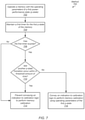
Referring to FIG. 7, a generalized flow diagram of one embodiment of a method 700 for efficiently handling memory calibration with transitions of power-performance states is shown. A memory operates with the operating parameters of a first power-performance state (p-state) (block 702). Logic, such as logic within a memory controller for the memory, maintains a first timer for the first p-state of the memory (block 704). If the logic determines that the first timer has not expired (“no” block of the conditional block 706), then the logic prevents conveying an indication to calibration logic to perform memory calibration (block 714).
If the logic determines that the first timer has expired (“yes” block of the conditional block 706), and another p-state transition will occur within a threshold amount of time (“yes” block of the conditional block 710), then the logic prevents conveyance of an indication to calibration logic to perform memory calibration (block 714). Otherwise, if the logic determines that the first timer has expired (“yes” block of the conditional block 706) and another p-state transition will not occur within a threshold amount of time (“no” block of the conditional block 710), then the logic conveys an indication to calibration logic to perform memory calibration using operating parameters of the first p-state (block 716).
Turning now to FIG. 8, a generalized block diagram of one embodiment of a computing system 800 capable of efficiently handling memory calibration with transitions of power-performance states is shown. As shown, a communication fabric 810 routes data between the input/output (I/O) interface 802, the memory interface 830, the power manager 820 and the processor complexes 860A-860B. In various embodiments, the computing system 800 is a system on chip (SoC) that includes multiple types of integrated circuits on a single semiconductor die, each integrated circuit providing a separate functionality. In other embodiments, the multiple functional units are individual dies within a package, such as a multi-chip module (MCM). In yet other embodiments, the multiple functional units are individual dies or chips on a printed circuit board.
Clock sources, such as phase lock loops (PLLs), interrupt controllers, and so forth are not shown in FIG. 8 for ease of illustration. It is also noted that the number of components of the computing system 800 (and the number of subcomponents for those shown in FIG. 8, such as within each of the processor complexes 860A-860B) may vary from embodiment to embodiment. There may be more or fewer of each component/subcomponent than the number shown for the computing system 800. As described earlier, the term “processor complex” is used to denote a configuration of one or more processor cores using local storage, such as a shared cache memory subsystem, and capable of processing a workload together.
The power manager 820 controls the supply voltage magnitudes requested from the external power management unit. There may be multiple supply voltages generated by the external power management unit for the computing system 800. For example, in the illustrated embodiment, there is a supply voltage indicated as VComplex for each of the processor complexes 860A-860B, a supply voltage Vmemory for the memory 840, and a supply voltage VSystem for one or more other components in the computing system 800. There may be multiple supply voltages for the rest of the computing system 800, in some embodiments.
In some embodiments, logic local to various components may control the power states of the components, including power up and power down and various other power-performance states (p-states) and operating modes for those components that support more than one p-state and operating mode. In various embodiments, the p-state is used to determine the operational voltage and operational frequency used by a component, whereas the operating mode determines how many sub-components are powered up such as particular execution pipelines.
In various embodiments, each of the processor complexes 860A-860B and the memory 840 are capable of operating with a different supply voltage from a different power plane (e.g., VComplexA≠VComplexB≠Vmemory). As shown, the processor complex 860A uses the voltage magnitude VComplexA as an operational supply voltage and the clock frequency FClock Domain A from a first clock domain. The processor complex 860B uses the voltage magnitude VComplexB as an operational supply voltage and the clock frequency FClock Domain B from a different, second clock domain. The memory 840 uses the voltage magnitude Vmemory as an operational supply voltage and the clock frequency FClock memory from a different, third clock domain. In other embodiments, each of the processor complexes 860A-860B and the memory 840 operates with a same supply voltage (e.g., VComplexA=VComplexB=Vmemory) from a single power plane while also operating with different clock frequencies source from different clock domains. In yet other embodiments, two or more of the processor complexes 860A-860B and the memory 840 operate with a same supply voltage and a same clock frequency while one other component operates with a different supply voltage or a different clock frequency.
In various embodiments, different types of data flow independently through the fabric 810. The independent flow is accomplished by allowing a single physical fabric bus to include a number of overlaying virtual channels, or dedicated source and destination buffers, each carrying a different type of data. Each channel is independently flow controlled with no dependence between transactions in different channels. The fabric 810 may also be packet-based, and may be hierarchical with bridges, cross bar, point-to-point, or other interconnects.
In some embodiments, the memory interface 830 uses at least one memory controller and at least one cache for the off-chip memory, such as synchronous DRAM (SDRAM). The memory interface 830 stores memory requests in request queues, uses any number of memory ports, and uses circuitry capable of interfacing to memory using one or more of a variety of protocols used to interface with memory channels used to interface to memory devices (not shown). The memory interface 830 may be responsible for the timing of the signals, for proper clocking to synchronous dynamic random access memory (SDRAM), on-die flash memory, etc. In various embodiments, the memory interface 830 also includes the calibration filter 832. In some embodiments, the functionality of the calibration filter 832 is equivalent to the functionality of the calibration filter 254 (of FIG. 2).
In various embodiments, one or more of the memory interface 830, an interrupt controller (not shown), and the fabric 810 uses control logic to ensure coherence among the different processor complexes 860A-860B and peripheral devices. In some embodiments, this circuitry uses cache coherency logic employing a cache coherency protocol to ensure data accessed by each source is kept up to date. An example of a cache coherency protocol includes the MOESI protocol with the Modified (M), Owned (0), Exclusive (E), Shared (S), and Invalid (I) states.
Although a single memory 840 is shown, computing system 800 may include multiple memory components arranged in a memory hierarchy. For example, memory 840 may include one or more of a shared last-level cache if it is not included in the memory interface 830, an SDRAM or other type of RAM, on-die flash memory, and so forth. In various designs, the memory 840 stores one or more applications. In an example, a copy of at least a portion of an application is loaded into an instruction cache in one of the processors 870A-870B when the application is selected by a base operating system (OS) for execution.
Memory 840 also stores source data for applications in addition to result data and intermediate data generated during the execution of applications. A virtual address space for the data stored in memory 840 and used by a software process is typically divided into pages of a prefixed size. The virtual pages are mapped to frames of physical memory. The mappings of virtual addresses to physical addresses, where virtual pages are loaded in the physical memory, are stored in a page table in memory 840. Each of translation look-aside buffers (TLBs) 868 and TLBs within the processors 870A-870B stores a subset of the page table.
In some embodiments, the components 862-878 of the processor complex 860A are similar to the components in the processor complex 860B. In other embodiments, the components in the processor complex 860B are designed for lower power consumption, and therefore, include control logic and processing capability producing less performance. For example, supported clock frequencies may be less than supported clock frequencies in the processor complex 860A. In addition, one or more of the processors in processor complex 860B may include a smaller number of execution pipelines and/or functional blocks for processing relatively high power consuming instructions than what is supported by the processors 870A-870B in the processor complex 860A.
As shown, processor complex 860A uses a fabric interface unit (FIU) 862 for providing memory access requests and responses to at least the processors 870A-870B. Processor complex 860A also supports a cache memory subsystem which includes at least cache 866. In some embodiments, the cache 866 is a shared off-die level two (L2) cache for the processors 870A-870B although an L3 cache is also possible and contemplated.
In some embodiments, the processors 870A-870B use a homogeneous architecture. For example, each of the processors 870A-870B is a general-purpose processor, such as a central processing unit (CPU), which utilizes circuitry for executing instructions according to a predefined general-purpose instruction set. Any of a variety of instruction set architectures (ISAs) may be selected. In some embodiments, each core within processors 870A-870B supports the out-of-order execution of one or more threads of a software process and include a multi-stage pipeline. The processors 870A-870B may support the execution of a variety of operating systems.
In other embodiments, the processors 870A-870B use a heterogeneous architecture. In such embodiments, one or more of the processors 870A-870B is a highly parallel data architected processor, rather than a CPU. In some embodiments, these other processors of the processors 870A-870B use single instruction multiple data (SIMD) cores. Examples of SIMD cores are graphics processing units (GPUs), digital signal processing (DSP) cores, or otherwise.
In various embodiments, each one of the processors 870A-870B uses one or more cores and one or more levels of a cache memory subsystem. The processors 870A-870B use multiple one or more on-die levels (L1, L2, L3 and so forth) of caches for accessing data and instructions. If a requested block is not found in the on-die caches or in the off-die cache 866, then a read request for the missing block is generated and transmitted to the memory interface 830 via fabric 810.
Turning next to FIG. 9, a block diagram of one embodiment of a system 900 is shown. As shown, system 900 represents chip, circuitry, components, etc., of a desktop computer 910, laptop computer 920, tablet computer 930, cell or mobile phone 940, television 950 (or set top box coupled to a television), wrist watch or other wearable item 960, or otherwise. Other devices are possible and are contemplated. In the illustrated embodiment, the system 900 includes at least one instance of a system on chip (SoC) 906 which includes multiple processors and a communication fabric. In some embodiments, one or more of SoC 906 and external memory 902 includes a memory controller similar to memory controller 230 (of FIG. 2) or memory interface 830 of computing system 800 (of FIG. 8). In various embodiments, SoC 906 is coupled to external memory 902, peripherals 904, and power supply 908.
The power supply 908 provides the supply voltages to SoC 906 as well as one or more supply voltages to the memory 902 and/or the peripherals 904. In various embodiments, power supply 908 represents a battery (e.g., a rechargeable battery in a smart phone, laptop or tablet computer). In some embodiments, more than one instance of SoC 906 is included (and more than one external memory 902 is included as well).
The memory 902 is any type of memory, such as dynamic random access memory (DRAM), synchronous DRAM (SDRAM), double data rate (DDR, DDR2, DDR3, etc.) SDRAM (including mobile versions of the SDRAMs such as mDDR3, etc., and/or low power versions of the SDRAMs such as LPDDR2, etc.), RAMBUS DRAM (RDRAM), static RAM (SRAM), etc. One or more memory devices are coupled onto a circuit board to form memory modules such as single inline memory modules (SIMMs), dual inline memory modules (DIMMs), etc. Alternatively, the devices are mounted with a SoC or an integrated circuit in a chip-on-chip configuration, a package-on-package configuration, or a multi-chip module configuration.
The peripherals 904 include any desired circuitry, depending on the type of system 900. For example, in one embodiment, peripherals 904 includes devices for various types of wireless communication, such as Wi-Fi, Bluetooth, cellular, global positioning system, etc. In some embodiments, the peripherals 904 also include additional storage, including RAM storage, solid-state storage, or disk storage. The peripherals 904 include user interface devices such as a display screen, including touch display screens or multitouch display screens, keyboard or other input devices, microphones, speakers, etc.
In various embodiments, program instructions of a software application may be used to implement the methods and/or mechanisms previously described. The program instructions describe the behavior of hardware in a high-level programming language, such as C. Alternatively, a hardware design language (HDL) is used, such as Verilog. The program instructions are stored on a non-transitory computer readable storage medium. Numerous types of storage media are available. The storage medium is accessible by a computer during use to provide the program instructions and accompanying data to the computer for program execution. In some embodiments, a synthesis tool reads the program instructions in order to produce a netlist including a list of gates from a synthesis library.
It should be emphasized that the above-described embodiments are only non-limiting examples of implementations. Numerous variations and modifications will become apparent to those skilled in the art once the above disclosure is fully appreciated. It is intended that the following claims be interpreted to embrace all such variations and modifications.

Claims (20)

What is claimed is:
1. An apparatus comprising:
a timer corresponding to a first power-performance state (p-state) of a plurality of p-states of a memory; and
circuitry configured to:
transfer data with the memory while the memory is operating in a second e-state different from the first p-state; and
responsive to receipt of a first indication to transition the memory from the second p-state to the first p-state:
inspect the timer; and
prevent calibration of the memory based at least in part on making
a determination that the timer has not expired after inspecting the timer.
2. The apparatus as recited in claim 1, wherein in based at least in part on a determination that calibration of the memory is prevented, the circuitry is further configured to convey a second indication to one or more agents that a latency for the transition to the first p-state does not include an added latency for memory calibration.
3. The apparatus as recited in claim 1, wherein the circuitry is further configured to prevent calibration of the memory based at least in part on:
receipt of an indication specifying to transition the memory to using operating parameters of the first p-state; and
a determination that:
the timer has expired, upon inspection of the timer responsive to receipt of the indication; and
another transition to another p-state will occur within a threshold amount of time.
4. The apparatus as recited in claim 1, wherein the circuitry is further configured to permit calibration of the memory based at least in part on:
receipt of an indication to transition the memory to using operating parameters of the first p-state; and
a determination that the timer has expired, upon inspection of the timer responsive to receipt of the indication.
5. The apparatus as recited in claim 4, wherein based at least in part on a determination that the calibration of the memory has completed, the circuitry is further configured to initialize the timer to indicate a duration during which memory calibration is not to be performed.
6. The apparatus as recited in claim 5, wherein the circuitry is further configured to update the timer while transferring data with the memory using operating parameters of the first p-state.
7. The apparatus as recited in claim 5, wherein in response to receiving an indication to transition the memory to using operating parameters of another p-state different from the first p-sate, the circuitry is further configured to prevent updating the first timer.
8. The apparatus as recited in claim 5, wherein the apparatus further comprises a respective timer for each of the plurality of p-states.
9. A method, comprising:
maintaining, by circuitry in a memory controller, a first timer corresponding to a first power-performance state (p-state) of a plurality of p-states of a memory;
receiving, by the circuitry, memory requests from one or more agents;
transferring, by the circuitry, data with the memory while the memory is operating in a second p-state different from the first p-state; and
in response to receiving, by the circuitry, a first indication to transition the memory from the second p-state to the first p-state:
inspecting, by the circuitry, the timer; and
preventing, by the circuitry, calibration of the memory based at least in part on making a determination that the timer has not expired after inspecting the timer.
10. The method as recited in claim 9, wherein in response to preventing calibration of the memory, the method further comprises conveying a second indication to the one or more agents that a latency for the transition to the first p-state does not include an added latency for memory calibration.
11. The method as recited in claim 9, further comprising preventing calibration of the memory responsive to:
receiving an indication specifying to transition the memory to using operating parameters of the first p-state; and
determining:
the timer has expired, upon inspecting the timer responsive to receiving the first indication; and
another transition to another p-state will occur within a threshold amount of time.
12. The method as recited in claim 11, wherein in response to determining the calibration of the memory has completed, the method further comprises initializing the timer to indicate a duration during which memory calibration is not to be performed.
13. The method as recited in claim 12, further comprising updating the timer while transferring data with the memory using operating parameters of the first p-state.
14. The method as recited in claim 12, wherein in response to receiving an indication to transition the memory to using operating parameters of another p-state different from the first p-sate, the method further comprises preventing updating the timer.
15. The method as recited in claim 12, further comprising maintaining a respective timer for each of the plurality of p-states.
16. A computing system comprising:
one or more agents, each configured to generate memory requests;
a memory controller;
a memory configured to store data requested by the one or more agents;
a power manager configured to send updated power-performance states (p-states) to the one or more agents and the memory; and
wherein the memory controller is configured to:
maintain a timer corresponding to a first p-state of a plurality of p-states of the memory;
receive memory requests from the one or more agents;
transfer data with the memory while the memory is operating in a second e-state different from the first p-state; and
responsive to receipt of a first indication to transition the memory from the second p-state to the first p-state:
inspect the timer; and
prevent calibration of the memory based at least in part on making a determination that the timer has not expired after inspecting the timer.
17. The computing system as recited in claim 16, wherein in response to preventing calibration of the memory, the memory controller is further configured to convey a second indication to one or more agents that a latency for the transition to the first p-state does not include an added latency for memory calibration.
18. The computing system as recited in claim 16, wherein the memory controller is further configured to prevent calibration of the memory responsive to:
receiving an indication specifying to transition the memory to using operating parameters of the first p-state; and
determining:
the timer has expired, upon inspecting the timer responsive to receiving the first indication; and
another transition to another p-state will occur within a threshold amount of time.
19. The computing system as recited in claim 18, wherein in response to determining the calibration of the memory has completed, the memory controller is further configured to initialize the timer to indicate a duration during which memory calibration is not to be performed.
20. The computing system as recited in claim 18, wherein the memory controller is further configured to update the timer while transferring data with the memory using operating parameters of the first p-state.
US16/293,398 2019-03-05 2019-03-05 Filtering memory calibration Active 2039-10-13 US11226752B2 (en)

Priority Applications (1)

Application Number Priority Date Filing Date Title
US16/293,398 US11226752B2 (en) 2019-03-05 2019-03-05 Filtering memory calibration

Applications Claiming Priority (1)

Application Number Priority Date Filing Date Title
US16/293,398 US11226752B2 (en) 2019-03-05 2019-03-05 Filtering memory calibration

Publications (2)

Publication Number Publication Date
US20200285406A1 US20200285406A1 (en) 2020-09-10
US11226752B2 true US11226752B2 (en) 2022-01-18

Family

ID=72335242

Family Applications (1)

Application Number Title Priority Date Filing Date
US16/293,398 Active 2039-10-13 US11226752B2 (en) 2019-03-05 2019-03-05 Filtering memory calibration

Country Status (1)

Country Link
US (1) US11226752B2 (en)

Families Citing this family (2)

* Cited by examiner, † Cited by third party
Publication number Priority date Publication date Assignee Title
US11664062B2 (en) * 2020-07-24 2023-05-30 Advanced Micro Devices, Inc. Memory calibration system and method
KR20220019944A (en) * 2020-08-11 2022-02-18 삼성전자주식회사 Storage devices and methods of operating storage devices

Citations (86)

* Cited by examiner, † Cited by third party
Publication number Priority date Publication date Assignee Title
US6310814B1 (en) 1998-03-10 2001-10-30 Rambus, Inc. Rambus DRAM (RDRAM) apparatus and method for performing refresh operations
US6434081B1 (en) 2000-05-12 2002-08-13 Micron Technology, Inc. Calibration technique for memory devices
US20030081483A1 (en) * 2001-09-19 2003-05-01 Denise De Paor Dram refresh command operation
US20030154416A1 (en) 2002-02-11 2003-08-14 Laberge Paul A. Method and apparatus for data transfer
US20030204669A1 (en) * 2002-04-25 2003-10-30 Vasanth Ranganathan Method and apparatus for handling memory refresh and maintenance operations
US6704821B2 (en) 2000-07-05 2004-03-09 Stmicroelectronics S.R.L. Arbitration method and circuit architecture therefore
US20040123207A1 (en) 2002-12-19 2004-06-24 Intel Corporation Two dimensional data eye centering for source synchronous data transfers
US6931559B2 (en) 2001-12-28 2005-08-16 Intel Corporation Multiple mode power throttle mechanism
US20050235102A1 (en) * 2004-04-20 2005-10-20 Mikio Sakurai Memory controller, semiconductor integrated circuit device, microcomputer, and electronic equipment
US6958613B2 (en) * 2002-09-30 2005-10-25 Infineon Technologies Ag Method for calibrating semiconductor devices using a common calibration reference and a calibration circuit
US20060100806A1 (en) * 2004-11-10 2006-05-11 Matsushita Electric Industrial Co., Ltd. Enhanced system for electronic storage device calibrations
US20060104137A1 (en) * 2004-11-12 2006-05-18 International Business Machines Corporation Deferring refreshes during calibrations in XDRTM memory systems
US7064994B1 (en) * 2004-01-30 2006-06-20 Sun Microsystems, Inc. Dynamic memory throttling for power and thermal limitations
US20060164909A1 (en) 2005-01-24 2006-07-27 International Business Machines Corporation System, method and storage medium for providing programmable delay chains for a memory system
US7162376B2 (en) 2004-12-23 2007-01-09 Rambus Inc. Circuits, systems and methods for dynamic reference voltage calibration
US20070183243A1 (en) * 2006-02-07 2007-08-09 Nec Corporation Memory synchronization method and refresh control circuit
US20070226529A1 (en) 2006-03-21 2007-09-27 Mediatek Inc. Memory controller and device with data strobe calibration
US20070288182A1 (en) 2006-05-30 2007-12-13 Daniel Douriet Method for Detecting Noise Events in Systems with Time Variable Operating Points
US20080007319A1 (en) * 2006-06-21 2008-01-10 Cox Christopher E Thermal sensor having toggle control
US20080068911A1 (en) 2006-09-19 2008-03-20 Thomas Hughes System and method for providing swap path voltage and temperature compensation
US20080094918A1 (en) 2006-10-18 2008-04-24 Nec Electronics Corporation Memory read control circuit and control method thereof
US7405984B2 (en) 2006-09-19 2008-07-29 Lsi Corporation System and method for providing programmable delay read data strobe gating with voltage and temperature compensation
US20080276133A1 (en) 2007-05-02 2008-11-06 Andrew Hadley Software-Controlled Dynamic DDR Calibration
US7467255B2 (en) * 2006-03-30 2008-12-16 Mediatek Inc. Method for calibration of memory devices, and apparatus thereof
US20090034344A1 (en) 2007-08-02 2009-02-05 Rambus, Inc. Methods and apparatus for strobe signaling and edge detection thereof
US20090244996A1 (en) 2008-03-31 2009-10-01 Advanced Micro Devices, Inc. Circuit Using a Shared Delay Locked Loop (DLL) and Method Therefor
US20090289659A1 (en) * 2008-05-22 2009-11-26 Elpida Memory, Inc. Calibration circuit
US7652932B2 (en) 2007-07-19 2010-01-26 Mosaid Technologies Incorporated Memory system having incorrupted strobe signals
US20100329276A1 (en) 2009-06-30 2010-12-30 Ren Wang Energy efficient network forwarding
US20110075496A1 (en) 2009-09-25 2011-03-31 Infineon Technologies Ag Memory Controller Comprising Adjustable Transmitter Impedance
US20110119439A1 (en) * 2009-11-17 2011-05-19 International Business Machines Corporation Spacing Periodic Commands to a Volatile Memory for Increased Performance and Decreased Collision
US20110238870A1 (en) * 2008-12-03 2011-09-29 Rambus Inc. Memory System With Command Filtering
US20110249522A1 (en) 2010-04-13 2011-10-13 Welker James A Method and circuit for calibrating data capture in a memory controller
US20120005515A1 (en) 2009-02-12 2012-01-05 Vijay Janapa Reddi Adaptive event-guided system and method for avoiding voltage emergencies
US20120151247A1 (en) 2010-10-27 2012-06-14 International Business Machines Corporation Dynamic Fault Detection and Repair in a Data Communications Mechanism
US20120159230A1 (en) * 2010-12-17 2012-06-21 Hao Chen Mechanism for Updating Memory Controller Timing Parameters During a Frequency Change
US20120166839A1 (en) 2011-12-22 2012-06-28 Sodhi Inder M Method, apparatus, and system for energy efficiency and energy conservation including energy efficient processor thermal throttling using deep power down mode
US8228747B2 (en) 2008-11-19 2012-07-24 Renesas Electronics Corporation Delay adjustment device, semiconductor device and delay adjustment method
US20120300570A1 (en) 2009-09-03 2012-11-29 International Business Machines Corporation Advanced memory device having improved performance, reduced power and increased reliability
US20120331220A1 (en) 2010-09-24 2012-12-27 Bains Kuljit S Fast exit from dram self-refresh
US20130064025A1 (en) 2011-09-08 2013-03-14 Hao Chen Dynamic data strobe detection
US20130070363A1 (en) 2011-09-21 2013-03-21 Western Digital Technologies, Inc. Systems and methods for data throttling during disk drive power down
US20130076425A1 (en) 2010-06-08 2013-03-28 Kyung Suk Oh Integrated circuit device timing calibration
US8582374B2 (en) 2009-12-15 2013-11-12 Intel Corporation Method and apparatus for dynamically adjusting voltage reference to optimize an I/O system
US8588014B1 (en) 2011-05-31 2013-11-19 Altera Corporation Methods for memory interface calibration
US8630131B1 (en) 2012-07-30 2014-01-14 Altera Corporation Data strobe enable circuitry
US20140019792A1 (en) 2011-03-02 2014-01-16 Rambus Inc. Timing calibration for multimode i/o systems
US8667347B2 (en) 2008-12-31 2014-03-04 Rambus Inc. Active calibration for high-speed memory devices
US20140181429A1 (en) 2012-12-26 2014-06-26 Nvidia Corporation Multi-dimensional hardware data training between memory controller and memory
US8775725B2 (en) * 2010-12-06 2014-07-08 Intel Corporation Memory device refresh commands on the fly
US20140229666A1 (en) 2013-02-08 2014-08-14 Theodore Z. Schoenborn Memory subsystem i/o performance based on in-system empirical testing
US8947140B2 (en) 2013-03-12 2015-02-03 Uniquify, Inc. Continuous adaptive training for data interface timing calibration
US8949520B2 (en) 2009-01-22 2015-02-03 Rambus Inc. Maintenance operations in a DRAM
US9043539B2 (en) * 2009-09-11 2015-05-26 Ps4 Luxco S.A.R.L. Semiconductor device having a memory and calibration circuit that selectively adjusts an impedance of an output buffer dependent upon refresh commands
US20150169443A1 (en) * 2013-12-12 2015-06-18 Samsung Electronics Co., Ltd. Non-volatile memory system, mobile apparatus including the same, and method of operating the non-volatile memory system
US9104421B2 (en) * 2012-07-30 2015-08-11 Nvidia Corporation Training, power-gating, and dynamic frequency changing of a memory controller
US9209961B1 (en) 2014-09-29 2015-12-08 Apple Inc. Method and apparatus for delay compensation in data transmission
US20160034219A1 (en) * 2014-08-04 2016-02-04 Apple Inc. System and method of calibration of memory interface during low power operation
US20160035411A1 (en) 2014-08-04 2016-02-04 Realtek Semiconductor Corp. Memory control circuit and associated memory control method
US20160048334A1 (en) 2014-08-18 2016-02-18 Apple Inc. System and method for calibration of a memory interface
US9286961B1 (en) 2015-03-30 2016-03-15 Apple Inc. Memory controller half-clock delay adjustment
US9305622B1 (en) 2015-01-23 2016-04-05 Apple Inc. Data strobe to data delay calibration
US20160118103A1 (en) 2013-11-07 2016-04-28 Renesas Eletronics Corporation Semiconductor device
US9396778B1 (en) 2015-08-07 2016-07-19 Apple Inc. Conditional memory calibration cancellation
US20160209866A1 (en) 2015-01-15 2016-07-21 Apple Inc. Calibration of Clock Signal for Data Transmission
US9401189B1 (en) 2013-03-15 2016-07-26 Altera Corporation Methods and apparatus for performing runtime data eye monitoring and continuous data strobe calibration
US20160292094A1 (en) 2015-04-01 2016-10-06 Apple Inc. Reference voltage calibration using a qualified weighted average
US20160351246A1 (en) 2013-06-26 2016-12-01 Micron Technology, Inc. Semiconductor device suppressing bti deterioration
US20170017274A1 (en) 2013-03-12 2017-01-19 International Business Machines Corporation 276-pin buffered memory card with enhanced memory system interconnect
US9558850B1 (en) 2015-12-01 2017-01-31 International Business Machines Corporation Efficient calibration of a data eye for memory devices
US9620184B1 (en) 2015-12-16 2017-04-11 International Business Machines Corporation Efficient calibration of memory devices
US20170236569A1 (en) * 2010-07-29 2017-08-17 Renesas Electronics Corporation Semiconductor device and data processing system with coordinated calibration and refresh operations
US20180046389A1 (en) 2016-08-11 2018-02-15 SK Hynix Inc. Memory controller and memory system including the same
US9928890B2 (en) 2016-08-29 2018-03-27 Apple Inc. System and method for calibrating memory using credit-based segmentation control
US9990973B1 (en) * 2017-02-17 2018-06-05 Apple Inc. Systems and methods using neighboring sample points in memory subsystem calibration
US20180181334A1 (en) * 2016-12-28 2018-06-28 Intel Corporation Memory controller capable of performing scheduled memory maintenance from a sleep state
US10037073B1 (en) * 2016-09-23 2018-07-31 Apple Inc. Execution unit power management
US10082823B1 (en) 2017-10-11 2018-09-25 Integrated Device Technology, Inc. Open loop solution in data buffer and RCD
US10083736B1 (en) 2016-06-23 2018-09-25 Apple Inc. Adaptive calibration scheduling for a memory subsystem based on calibrations of delay applied to data strobe and calibration of reference voltage
US10110210B2 (en) 2016-12-16 2018-10-23 Intel Corporation Apparatus and method for strobe centering for source synchronous links
US10242723B1 (en) 2017-12-19 2019-03-26 Apple Inc. Method and apparatus for background memory subsystem calibration
US10270429B1 (en) 2017-12-20 2019-04-23 Micron Technology, Inc. Internal clock distortion calibration using DC component offset of clock signal
US20190187189A1 (en) * 2017-12-20 2019-06-20 Apple Inc. Reference Voltage Prediction in Memory Subsystem
US10636383B2 (en) * 2017-04-24 2020-04-28 Beijing Xiaomi Mobile Software Co., Ltd. Method, apparatus and device for adjusting screen color and storage medium
US20200286567A1 (en) * 2019-03-07 2020-09-10 Micron Technology, Inc. Adjustment of program verify targets corresponding to a last programming distribution and a programming distribution adjacent to an initial programming distribution
US10872652B2 (en) 2018-06-19 2020-12-22 Apple Inc. Method and apparatus for optimizing calibrations of a memory subsystem

Patent Citations (98)

* Cited by examiner, † Cited by third party
Publication number Priority date Publication date Assignee Title
US6310814B1 (en) 1998-03-10 2001-10-30 Rambus, Inc. Rambus DRAM (RDRAM) apparatus and method for performing refresh operations
US6434081B1 (en) 2000-05-12 2002-08-13 Micron Technology, Inc. Calibration technique for memory devices
US6704821B2 (en) 2000-07-05 2004-03-09 Stmicroelectronics S.R.L. Arbitration method and circuit architecture therefore
US20030081483A1 (en) * 2001-09-19 2003-05-01 Denise De Paor Dram refresh command operation
US6931559B2 (en) 2001-12-28 2005-08-16 Intel Corporation Multiple mode power throttle mechanism
US20030154416A1 (en) 2002-02-11 2003-08-14 Laberge Paul A. Method and apparatus for data transfer
US20030204669A1 (en) * 2002-04-25 2003-10-30 Vasanth Ranganathan Method and apparatus for handling memory refresh and maintenance operations
US6958613B2 (en) * 2002-09-30 2005-10-25 Infineon Technologies Ag Method for calibrating semiconductor devices using a common calibration reference and a calibration circuit
US7036053B2 (en) 2002-12-19 2006-04-25 Intel Corporation Two dimensional data eye centering for source synchronous data transfers
US20040123207A1 (en) 2002-12-19 2004-06-24 Intel Corporation Two dimensional data eye centering for source synchronous data transfers
US7064994B1 (en) * 2004-01-30 2006-06-20 Sun Microsystems, Inc. Dynamic memory throttling for power and thermal limitations
US20050235102A1 (en) * 2004-04-20 2005-10-20 Mikio Sakurai Memory controller, semiconductor integrated circuit device, microcomputer, and electronic equipment
US20060100806A1 (en) * 2004-11-10 2006-05-11 Matsushita Electric Industrial Co., Ltd. Enhanced system for electronic storage device calibrations
US20080140923A1 (en) * 2004-11-12 2008-06-12 Mark David Bellows Deferring Refreshes During Calibrations in Memory Systems
US20060104137A1 (en) * 2004-11-12 2006-05-18 International Business Machines Corporation Deferring refreshes during calibrations in XDRTM memory systems
US7162376B2 (en) 2004-12-23 2007-01-09 Rambus Inc. Circuits, systems and methods for dynamic reference voltage calibration
US20060164909A1 (en) 2005-01-24 2006-07-27 International Business Machines Corporation System, method and storage medium for providing programmable delay chains for a memory system
US20070183243A1 (en) * 2006-02-07 2007-08-09 Nec Corporation Memory synchronization method and refresh control circuit
US20070226529A1 (en) 2006-03-21 2007-09-27 Mediatek Inc. Memory controller and device with data strobe calibration
US7698589B2 (en) * 2006-03-21 2010-04-13 Mediatek Inc. Memory controller and device with data strobe calibration
US7467255B2 (en) * 2006-03-30 2008-12-16 Mediatek Inc. Method for calibration of memory devices, and apparatus thereof
US20070288182A1 (en) 2006-05-30 2007-12-13 Daniel Douriet Method for Detecting Noise Events in Systems with Time Variable Operating Points
US20080007319A1 (en) * 2006-06-21 2008-01-10 Cox Christopher E Thermal sensor having toggle control
US7405984B2 (en) 2006-09-19 2008-07-29 Lsi Corporation System and method for providing programmable delay read data strobe gating with voltage and temperature compensation
US20080068911A1 (en) 2006-09-19 2008-03-20 Thomas Hughes System and method for providing swap path voltage and temperature compensation
US20080094918A1 (en) 2006-10-18 2008-04-24 Nec Electronics Corporation Memory read control circuit and control method thereof
US20080276133A1 (en) 2007-05-02 2008-11-06 Andrew Hadley Software-Controlled Dynamic DDR Calibration
US7652932B2 (en) 2007-07-19 2010-01-26 Mosaid Technologies Incorporated Memory system having incorrupted strobe signals
US20090034344A1 (en) 2007-08-02 2009-02-05 Rambus, Inc. Methods and apparatus for strobe signaling and edge detection thereof
US20090244996A1 (en) 2008-03-31 2009-10-01 Advanced Micro Devices, Inc. Circuit Using a Shared Delay Locked Loop (DLL) and Method Therefor
US20090289659A1 (en) * 2008-05-22 2009-11-26 Elpida Memory, Inc. Calibration circuit
US8228747B2 (en) 2008-11-19 2012-07-24 Renesas Electronics Corporation Delay adjustment device, semiconductor device and delay adjustment method
US20110238870A1 (en) * 2008-12-03 2011-09-29 Rambus Inc. Memory System With Command Filtering
US8667347B2 (en) 2008-12-31 2014-03-04 Rambus Inc. Active calibration for high-speed memory devices
US20160064066A1 (en) 2009-01-22 2016-03-03 Rambus Inc. Maintenance operations in a dram
US8949520B2 (en) 2009-01-22 2015-02-03 Rambus Inc. Maintenance operations in a DRAM
US20120005515A1 (en) 2009-02-12 2012-01-05 Vijay Janapa Reddi Adaptive event-guided system and method for avoiding voltage emergencies
US20100329276A1 (en) 2009-06-30 2010-12-30 Ren Wang Energy efficient network forwarding
US20120300570A1 (en) 2009-09-03 2012-11-29 International Business Machines Corporation Advanced memory device having improved performance, reduced power and increased reliability
US8452919B2 (en) 2009-09-03 2013-05-28 International Business Machines Corporation Advanced memory device having improved performance, reduced power and increased reliability
US9043539B2 (en) * 2009-09-11 2015-05-26 Ps4 Luxco S.A.R.L. Semiconductor device having a memory and calibration circuit that selectively adjusts an impedance of an output buffer dependent upon refresh commands
US20110075496A1 (en) 2009-09-25 2011-03-31 Infineon Technologies Ag Memory Controller Comprising Adjustable Transmitter Impedance
US8233336B2 (en) 2009-09-25 2012-07-31 Infineon Technologies Ag Memory controller comprising adjustable transmitter impedance
US20110119439A1 (en) * 2009-11-17 2011-05-19 International Business Machines Corporation Spacing Periodic Commands to a Volatile Memory for Increased Performance and Decreased Collision
US8582374B2 (en) 2009-12-15 2013-11-12 Intel Corporation Method and apparatus for dynamically adjusting voltage reference to optimize an I/O system
US20110249522A1 (en) 2010-04-13 2011-10-13 Welker James A Method and circuit for calibrating data capture in a memory controller
US20130076425A1 (en) 2010-06-08 2013-03-28 Kyung Suk Oh Integrated circuit device timing calibration
US20170236569A1 (en) * 2010-07-29 2017-08-17 Renesas Electronics Corporation Semiconductor device and data processing system with coordinated calibration and refresh operations
US10090028B2 (en) * 2010-07-29 2018-10-02 Renesas Electronics Corporation Semiconductor device and data processing system with coordinated calibration and refresh operations
US20120331220A1 (en) 2010-09-24 2012-12-27 Bains Kuljit S Fast exit from dram self-refresh
US20120151247A1 (en) 2010-10-27 2012-06-14 International Business Machines Corporation Dynamic Fault Detection and Repair in a Data Communications Mechanism
US8775725B2 (en) * 2010-12-06 2014-07-08 Intel Corporation Memory device refresh commands on the fly
US20120159230A1 (en) * 2010-12-17 2012-06-21 Hao Chen Mechanism for Updating Memory Controller Timing Parameters During a Frequency Change
US20140019792A1 (en) 2011-03-02 2014-01-16 Rambus Inc. Timing calibration for multimode i/o systems
US8588014B1 (en) 2011-05-31 2013-11-19 Altera Corporation Methods for memory interface calibration
US20130064025A1 (en) 2011-09-08 2013-03-14 Hao Chen Dynamic data strobe detection
US20130070363A1 (en) 2011-09-21 2013-03-21 Western Digital Technologies, Inc. Systems and methods for data throttling during disk drive power down
US20120166839A1 (en) 2011-12-22 2012-06-28 Sodhi Inder M Method, apparatus, and system for energy efficiency and energy conservation including energy efficient processor thermal throttling using deep power down mode
US9104421B2 (en) * 2012-07-30 2015-08-11 Nvidia Corporation Training, power-gating, and dynamic frequency changing of a memory controller
US8630131B1 (en) 2012-07-30 2014-01-14 Altera Corporation Data strobe enable circuitry
US20140181429A1 (en) 2012-12-26 2014-06-26 Nvidia Corporation Multi-dimensional hardware data training between memory controller and memory
US20140229666A1 (en) 2013-02-08 2014-08-14 Theodore Z. Schoenborn Memory subsystem i/o performance based on in-system empirical testing
US8947140B2 (en) 2013-03-12 2015-02-03 Uniquify, Inc. Continuous adaptive training for data interface timing calibration
US20170017274A1 (en) 2013-03-12 2017-01-19 International Business Machines Corporation 276-pin buffered memory card with enhanced memory system interconnect
US9425778B2 (en) 2013-03-12 2016-08-23 Uniquify, Inc. Continuous adaptive data capture optimization for interface circuits
US9401189B1 (en) 2013-03-15 2016-07-26 Altera Corporation Methods and apparatus for performing runtime data eye monitoring and continuous data strobe calibration
US20160351246A1 (en) 2013-06-26 2016-12-01 Micron Technology, Inc. Semiconductor device suppressing bti deterioration
US9728246B2 (en) 2013-06-26 2017-08-08 Micron Technology, Inc. Semiconductor device suppressing BTI deterioration
US20160118103A1 (en) 2013-11-07 2016-04-28 Renesas Eletronics Corporation Semiconductor device
US20150169443A1 (en) * 2013-12-12 2015-06-18 Samsung Electronics Co., Ltd. Non-volatile memory system, mobile apparatus including the same, and method of operating the non-volatile memory system
US20160034219A1 (en) * 2014-08-04 2016-02-04 Apple Inc. System and method of calibration of memory interface during low power operation
US20160035411A1 (en) 2014-08-04 2016-02-04 Realtek Semiconductor Corp. Memory control circuit and associated memory control method
US20160048334A1 (en) 2014-08-18 2016-02-18 Apple Inc. System and method for calibration of a memory interface
US9436387B2 (en) 2014-08-18 2016-09-06 Apple Inc. System and method for calibration of a memory interface
US9209961B1 (en) 2014-09-29 2015-12-08 Apple Inc. Method and apparatus for delay compensation in data transmission
US20160209866A1 (en) 2015-01-15 2016-07-21 Apple Inc. Calibration of Clock Signal for Data Transmission
US9477259B2 (en) 2015-01-15 2016-10-25 Apple Inc. Calibration of clock signal for data transmission
US9305622B1 (en) 2015-01-23 2016-04-05 Apple Inc. Data strobe to data delay calibration
US9286961B1 (en) 2015-03-30 2016-03-15 Apple Inc. Memory controller half-clock delay adjustment
US20160292094A1 (en) 2015-04-01 2016-10-06 Apple Inc. Reference voltage calibration using a qualified weighted average
US9396778B1 (en) 2015-08-07 2016-07-19 Apple Inc. Conditional memory calibration cancellation
US9627030B1 (en) 2015-12-01 2017-04-18 International Business Machines Corporation Efficient calibration of a data eye for memory devices
US9558850B1 (en) 2015-12-01 2017-01-31 International Business Machines Corporation Efficient calibration of a data eye for memory devices
US9620184B1 (en) 2015-12-16 2017-04-11 International Business Machines Corporation Efficient calibration of memory devices
US10083736B1 (en) 2016-06-23 2018-09-25 Apple Inc. Adaptive calibration scheduling for a memory subsystem based on calibrations of delay applied to data strobe and calibration of reference voltage
US20180046389A1 (en) 2016-08-11 2018-02-15 SK Hynix Inc. Memory controller and memory system including the same
US9928890B2 (en) 2016-08-29 2018-03-27 Apple Inc. System and method for calibrating memory using credit-based segmentation control
US10037073B1 (en) * 2016-09-23 2018-07-31 Apple Inc. Execution unit power management
US10110210B2 (en) 2016-12-16 2018-10-23 Intel Corporation Apparatus and method for strobe centering for source synchronous links
US20180181334A1 (en) * 2016-12-28 2018-06-28 Intel Corporation Memory controller capable of performing scheduled memory maintenance from a sleep state
US9990973B1 (en) * 2017-02-17 2018-06-05 Apple Inc. Systems and methods using neighboring sample points in memory subsystem calibration
US10636383B2 (en) * 2017-04-24 2020-04-28 Beijing Xiaomi Mobile Software Co., Ltd. Method, apparatus and device for adjusting screen color and storage medium
US10082823B1 (en) 2017-10-11 2018-09-25 Integrated Device Technology, Inc. Open loop solution in data buffer and RCD
US10242723B1 (en) 2017-12-19 2019-03-26 Apple Inc. Method and apparatus for background memory subsystem calibration
US10270429B1 (en) 2017-12-20 2019-04-23 Micron Technology, Inc. Internal clock distortion calibration using DC component offset of clock signal
US20190187189A1 (en) * 2017-12-20 2019-06-20 Apple Inc. Reference Voltage Prediction in Memory Subsystem
US10872652B2 (en) 2018-06-19 2020-12-22 Apple Inc. Method and apparatus for optimizing calibrations of a memory subsystem
US20200286567A1 (en) * 2019-03-07 2020-09-10 Micron Technology, Inc. Adjustment of program verify targets corresponding to a last programming distribution and a programming distribution adjacent to an initial programming distribution

Non-Patent Citations (3)

* Cited by examiner, † Cited by third party
Title
International Search Report and Written Opinion in International Application No. PCT/US2016/020197, dated Jun. 14, 2016, 13 pages.
J. Huang and R. Liu, "DI-SSD: Desymmetrized Interconnection Architecture and Dynamic Timing Calibration for Solid-State Drives", 2018 23rd Asia and South Pacific Design Automation Conference (ASP-DAC), 2018, pp. 34-39 (Year: 2018). *
Self-Calibrating Memory Controllers; William G. Wong, ElectronicDesign; May 16, 2011; retrieved from https://www.electronicdesign.com/technologies/boards/article/21799302/selfcalibrating-memory-controllers on Jul. 2, 2021 (Year: 2011). *

Also Published As

Publication number Publication date
US20200285406A1 (en) 2020-09-10

Similar Documents

Publication Publication Date Title
US10872652B2 (en) Method and apparatus for optimizing calibrations of a memory subsystem
US10510396B1 (en) Method and apparatus for interrupting memory bank refresh
US10048720B2 (en) Timebase synchronization
AU2012216673B8 (en) Dynamic data strobe detection
US8468373B2 (en) Modifying performance parameters in multiple circuits according to a performance state table upon receiving a request to change a performance state
US8769332B2 (en) Regional clock gating and dithering
US20120159230A1 (en) Mechanism for Updating Memory Controller Timing Parameters During a Frequency Change
US20050066141A1 (en) Method and apparatus for accessing a dynamic memory device
US9436387B2 (en) System and method for calibration of a memory interface
US8892922B2 (en) Voltage detection
US10649922B2 (en) Systems and methods for scheduling different types of memory requests with varying data sizes
US10255218B1 (en) Systems and methods for maintaining specific ordering in bus traffic
US11226752B2 (en) Filtering memory calibration
US9659616B2 (en) Configuration fuse data management in a partial power-on state
US20180061484A1 (en) Systems and Methods for Memory Refresh Timing
US10725928B1 (en) Translation lookaside buffer invalidation by range
US11221962B2 (en) Unified address translation
US20230112432A1 (en) Dynamic setup and hold times adjustment for memories
US11934251B2 (en) Data fabric clock switching
US11169585B2 (en) Dashboard with push model for receiving sensor data
US10304530B2 (en) Per-pin compact reference voltage generator
US10552323B1 (en) Cache flush method and apparatus
US20140197870A1 (en) Reset extender for divided clock domains
US20240004560A1 (en) Efficient memory power control operations

Legal Events

Date Code Title Description
AS Assignment

Owner name: APPLE INC., CALIFORNIA

Free format text: ASSIGNMENT OF ASSIGNORS INTEREST;ASSIGNORS:NOTANI, RAKESH L.;JETER, ROBERT E.;SUVARNA RAMESH, SUHAS KUMAR;AND OTHERS;SIGNING DATES FROM 20190304 TO 20190305;REEL/FRAME:048510/0140

FEPP Fee payment procedure

Free format text: ENTITY STATUS SET TO UNDISCOUNTED (ORIGINAL EVENT CODE: BIG.); ENTITY STATUS OF PATENT OWNER: LARGE ENTITY

STPP Information on status: patent application and granting procedure in general

Free format text: NON FINAL ACTION MAILED

STPP Information on status: patent application and granting procedure in general

Free format text: RESPONSE TO NON-FINAL OFFICE ACTION ENTERED AND FORWARDED TO EXAMINER

STPP Information on status: patent application and granting procedure in general

Free format text: NOTICE OF ALLOWANCE MAILED -- APPLICATION RECEIVED IN OFFICE OF PUBLICATIONS

STPP Information on status: patent application and granting procedure in general

Free format text: PUBLICATIONS -- ISSUE FEE PAYMENT VERIFIED

STCF Information on status: patent grant

Free format text: PATENTED CASE

CC Certificate of correction