EP2168008B1 - Spacer lithography - Google Patents
Spacer lithography Download PDFInfo
- Publication number
- EP2168008B1 EP2168008B1 EP08780091.8A EP08780091A EP2168008B1 EP 2168008 B1 EP2168008 B1 EP 2168008B1 EP 08780091 A EP08780091 A EP 08780091A EP 2168008 B1 EP2168008 B1 EP 2168008B1
- Authority
- EP
- European Patent Office
- Prior art keywords
- cross
- mask pattern
- layer
- acid
- forming
- Prior art date
- Legal status (The legal status is an assumption and is not a legal conclusion. Google has not performed a legal analysis and makes no representation as to the accuracy of the status listed.)
- Active
Links
- 125000006850 spacer group Chemical group 0.000 title claims description 36
- 238000001459 lithography Methods 0.000 title description 4
- 239000002253 acid Substances 0.000 claims description 30
- 238000004519 manufacturing process Methods 0.000 claims description 27
- 238000000034 method Methods 0.000 claims description 24
- 239000004065 semiconductor Substances 0.000 claims description 23
- 239000011368 organic material Substances 0.000 claims description 21
- 239000000463 material Substances 0.000 claims description 18
- 238000005530 etching Methods 0.000 claims description 17
- 238000006243 chemical reaction Methods 0.000 claims description 12
- 238000004132 cross linking Methods 0.000 claims description 10
- 238000010438 heat treatment Methods 0.000 claims description 8
- 229920005989 resin Polymers 0.000 claims description 6
- 239000011347 resin Substances 0.000 claims description 6
- 150000003839 salts Chemical class 0.000 claims description 4
- 239000003795 chemical substances by application Substances 0.000 claims description 3
- 229920003986 novolac Polymers 0.000 claims description 3
- 229920002120 photoresistant polymer Polymers 0.000 description 12
- 238000013461 design Methods 0.000 description 10
- 239000000203 mixture Substances 0.000 description 10
- 230000008901 benefit Effects 0.000 description 8
- DHKHKXVYLBGOIT-UHFFFAOYSA-N acetaldehyde Diethyl Acetal Natural products CCOC(C)OCC DHKHKXVYLBGOIT-UHFFFAOYSA-N 0.000 description 5
- 239000003431 cross linking reagent Substances 0.000 description 5
- 239000000126 substance Substances 0.000 description 5
- 238000000151 deposition Methods 0.000 description 4
- 230000015654 memory Effects 0.000 description 4
- -1 polyvinylamine Polymers 0.000 description 4
- 238000012545 processing Methods 0.000 description 4
- 229920002554 vinyl polymer Polymers 0.000 description 4
- 150000001241 acetals Chemical class 0.000 description 3
- 235000012431 wafers Nutrition 0.000 description 3
- XLYOFNOQVPJJNP-UHFFFAOYSA-N water Substances O XLYOFNOQVPJJNP-UHFFFAOYSA-N 0.000 description 3
- 229920000877 Melamine resin Polymers 0.000 description 2
- 239000011354 acetal resin Substances 0.000 description 2
- 230000015572 biosynthetic process Effects 0.000 description 2
- 230000002860 competitive effect Effects 0.000 description 2
- 230000003287 optical effect Effects 0.000 description 2
- 229920006324 polyoxymethylene Polymers 0.000 description 2
- 239000002904 solvent Substances 0.000 description 2
- 150000003672 ureas Chemical class 0.000 description 2
- YXIJVUMGHSCKIO-UHFFFAOYSA-N 1-(hydroxymethyl)-1-methoxyurea Chemical compound CON(CO)C(N)=O YXIJVUMGHSCKIO-UHFFFAOYSA-N 0.000 description 1
- 125000003504 2-oxazolinyl group Chemical group O1C(=NCC1)* 0.000 description 1
- XLLXMBCBJGATSP-UHFFFAOYSA-N 2-phenylethenol Chemical class OC=CC1=CC=CC=C1 XLLXMBCBJGATSP-UHFFFAOYSA-N 0.000 description 1
- PYSRRFNXTXNWCD-UHFFFAOYSA-N 3-(2-phenylethenyl)furan-2,5-dione Chemical compound O=C1OC(=O)C(C=CC=2C=CC=CC=2)=C1 PYSRRFNXTXNWCD-UHFFFAOYSA-N 0.000 description 1
- GZVHEAJQGPRDLQ-UHFFFAOYSA-N 6-phenyl-1,3,5-triazine-2,4-diamine Chemical compound NC1=NC(N)=NC(C=2C=CC=CC=2)=N1 GZVHEAJQGPRDLQ-UHFFFAOYSA-N 0.000 description 1
- 239000004971 Cross linker Substances 0.000 description 1
- 239000004593 Epoxy Substances 0.000 description 1
- LFQSCWFLJHTTHZ-UHFFFAOYSA-N Ethanol Chemical compound CCO LFQSCWFLJHTTHZ-UHFFFAOYSA-N 0.000 description 1
- JOYRKODLDBILNP-UHFFFAOYSA-N Ethyl urethane Chemical compound CCOC(N)=O JOYRKODLDBILNP-UHFFFAOYSA-N 0.000 description 1
- ISWSIDIOOBJBQZ-UHFFFAOYSA-N Phenol Chemical compound OC1=CC=CC=C1 ISWSIDIOOBJBQZ-UHFFFAOYSA-N 0.000 description 1
- 229920002873 Polyethylenimine Polymers 0.000 description 1
- 239000004372 Polyvinyl alcohol Substances 0.000 description 1
- 229920002125 Sokalan® Polymers 0.000 description 1
- 229920000147 Styrene maleic anhydride Polymers 0.000 description 1
- XSQUKJJJFZCRTK-UHFFFAOYSA-N Urea Chemical compound NC(N)=O XSQUKJJJFZCRTK-UHFFFAOYSA-N 0.000 description 1
- 229920001807 Urea-formaldehyde Polymers 0.000 description 1
- ONTAEZSXZGCILH-UHFFFAOYSA-N [(4,6-diamino-1,3,5-triazin-2-yl)-methoxyamino]methanol Chemical compound CON(CO)C1=NC(N)=NC(N)=N1 ONTAEZSXZGCILH-UHFFFAOYSA-N 0.000 description 1
- 238000006359 acetalization reaction Methods 0.000 description 1
- 239000003929 acidic solution Substances 0.000 description 1
- 230000002411 adverse Effects 0.000 description 1
- 229920000180 alkyd Polymers 0.000 description 1
- 238000000137 annealing Methods 0.000 description 1
- 239000004202 carbamide Substances 0.000 description 1
- 230000001413 cellular effect Effects 0.000 description 1
- 238000010894 electron beam technology Methods 0.000 description 1
- 230000001747 exhibiting effect Effects 0.000 description 1
- 238000007687 exposure technique Methods 0.000 description 1
- 230000006870 function Effects 0.000 description 1
- 230000003116 impacting effect Effects 0.000 description 1
- 239000012948 isocyanate Substances 0.000 description 1
- 150000002513 isocyanates Chemical class 0.000 description 1
- 230000007246 mechanism Effects 0.000 description 1
- JDSHMPZPIAZGSV-UHFFFAOYSA-N melamine Chemical compound NC1=NC(N)=NC(N)=N1 JDSHMPZPIAZGSV-UHFFFAOYSA-N 0.000 description 1
- 150000007974 melamines Chemical class 0.000 description 1
- 238000012986 modification Methods 0.000 description 1
- 230000004048 modification Effects 0.000 description 1
- 238000005498 polishing Methods 0.000 description 1
- 229920000083 poly(allylamine) Polymers 0.000 description 1
- 239000004584 polyacrylic acid Substances 0.000 description 1
- 229920002451 polyvinyl alcohol Polymers 0.000 description 1
- 229920000036 polyvinylpyrrolidone Polymers 0.000 description 1
- 239000001267 polyvinylpyrrolidone Substances 0.000 description 1
- 235000013855 polyvinylpyrrolidone Nutrition 0.000 description 1
- 125000002924 primary amino group Chemical group [H]N([H])* 0.000 description 1
- 230000008569 process Effects 0.000 description 1
- 230000005855 radiation Effects 0.000 description 1
- 229940124530 sulfonamide Drugs 0.000 description 1
- 150000003456 sulfonamides Chemical class 0.000 description 1
- 238000011282 treatment Methods 0.000 description 1
Images


Classifications
-
- G—PHYSICS
- G03—PHOTOGRAPHY; CINEMATOGRAPHY; ANALOGOUS TECHNIQUES USING WAVES OTHER THAN OPTICAL WAVES; ELECTROGRAPHY; HOLOGRAPHY
- G03F—PHOTOMECHANICAL PRODUCTION OF TEXTURED OR PATTERNED SURFACES, e.g. FOR PRINTING, FOR PROCESSING OF SEMICONDUCTOR DEVICES; MATERIALS THEREFOR; ORIGINALS THEREFOR; APPARATUS SPECIALLY ADAPTED THEREFOR
- G03F7/00—Photomechanical, e.g. photolithographic, production of textured or patterned surfaces, e.g. printing surfaces; Materials therefor, e.g. comprising photoresists; Apparatus specially adapted therefor
- G03F7/0035—Multiple processes, e.g. applying a further resist layer on an already in a previously step, processed pattern or textured surface
-
- G—PHYSICS
- G03—PHOTOGRAPHY; CINEMATOGRAPHY; ANALOGOUS TECHNIQUES USING WAVES OTHER THAN OPTICAL WAVES; ELECTROGRAPHY; HOLOGRAPHY
- G03F—PHOTOMECHANICAL PRODUCTION OF TEXTURED OR PATTERNED SURFACES, e.g. FOR PRINTING, FOR PROCESSING OF SEMICONDUCTOR DEVICES; MATERIALS THEREFOR; ORIGINALS THEREFOR; APPARATUS SPECIALLY ADAPTED THEREFOR
- G03F7/00—Photomechanical, e.g. photolithographic, production of textured or patterned surfaces, e.g. printing surfaces; Materials therefor, e.g. comprising photoresists; Apparatus specially adapted therefor
- G03F7/26—Processing photosensitive materials; Apparatus therefor
- G03F7/40—Treatment after imagewise removal, e.g. baking
-
- H—ELECTRICITY
- H01—ELECTRIC ELEMENTS
- H01L—SEMICONDUCTOR DEVICES NOT COVERED BY CLASS H10
- H01L21/00—Processes or apparatus adapted for the manufacture or treatment of semiconductor or solid state devices or of parts thereof
- H01L21/02—Manufacture or treatment of semiconductor devices or of parts thereof
- H01L21/027—Making masks on semiconductor bodies for further photolithographic processing not provided for in group H01L21/18 or H01L21/34
- H01L21/0271—Making masks on semiconductor bodies for further photolithographic processing not provided for in group H01L21/18 or H01L21/34 comprising organic layers
- H01L21/0273—Making masks on semiconductor bodies for further photolithographic processing not provided for in group H01L21/18 or H01L21/34 comprising organic layers characterised by the treatment of photoresist layers
- H01L21/0274—Photolithographic processes
-
- H—ELECTRICITY
- H01—ELECTRIC ELEMENTS
- H01L—SEMICONDUCTOR DEVICES NOT COVERED BY CLASS H10
- H01L21/00—Processes or apparatus adapted for the manufacture or treatment of semiconductor or solid state devices or of parts thereof
- H01L21/02—Manufacture or treatment of semiconductor devices or of parts thereof
- H01L21/04—Manufacture or treatment of semiconductor devices or of parts thereof the devices having potential barriers, e.g. a PN junction, depletion layer or carrier concentration layer
- H01L21/18—Manufacture or treatment of semiconductor devices or of parts thereof the devices having potential barriers, e.g. a PN junction, depletion layer or carrier concentration layer the devices having semiconductor bodies comprising elements of Group IV of the Periodic Table or AIIIBV compounds with or without impurities, e.g. doping materials
- H01L21/30—Treatment of semiconductor bodies using processes or apparatus not provided for in groups H01L21/20 - H01L21/26
- H01L21/31—Treatment of semiconductor bodies using processes or apparatus not provided for in groups H01L21/20 - H01L21/26 to form insulating layers thereon, e.g. for masking or by using photolithographic techniques; After treatment of these layers; Selection of materials for these layers
- H01L21/3205—Deposition of non-insulating-, e.g. conductive- or resistive-, layers on insulating layers; After-treatment of these layers
- H01L21/321—After treatment
- H01L21/3213—Physical or chemical etching of the layers, e.g. to produce a patterned layer from a pre-deposited extensive layer
- H01L21/32139—Physical or chemical etching of the layers, e.g. to produce a patterned layer from a pre-deposited extensive layer using masks
Definitions
- the present invention relates to the fabrication of semiconductor devices having accurately formed ultrafine design features.
- the present invention is particularly applicable to fabricating semiconductor devices having high speed integrated circuits with design features in the deep sub-micron range in an efficient manner with increased manufacturing throughput.
- Double exposure techniques that involve spacer lithographic processes have evolved. However, these techniques have not been completely successful and suffer from low manufacturing throughput, some techniques requiring the use of various tools and frequent chemical mechanical polishing (CMP). Transportation of a wafer from one tool to another and frequent use of CMP are not only time consuming but inevitably results in reduced yield thereby placing a chip maker at a disadvantage. In today's competitive market, a yield of at least 70% is required for profitability.
- An advantage of the present invention is a method of fabricating semiconductor devices having accurately formed features with dimensions in the deep sub-micron range.
- Another advantage of the present invention is an efficient method of fabricating semiconductor devices having accurately formed sub-micron features at high manufacturing throughput.
- Another advantage of the present invention is a method of fabricating a semiconductor device, the method comprising forming a first photoresist mask pattern over a target layer, the first mask pattern having upper and side surfaces and comprising a material capable of generating an acid; forming a cross-linkable layer, comprising a material capable of undergoing a cross-linking reaction in the presence of an acid, on the first photoresist mask pattern; generating an acid in the first photoresist mask pattern by heating or irradiation; heating to diffuse the acid to the cross-linkable layer to form a cross-linked spacer on the upper and side surfaces of the first photoresist mask pattern; removing portions of the cross-linkable layer to expose the cross-linked spacer on the upper surfaces of the first photoresist mask pattern and removing the exposed cross-linked spacer from the upper surfaces of the first photoresist mask pattern, leaving the cross-linked spacer on the side surfaces of the first photoresist mask pattern; removing remaining portions of the cross-linkable layer and removing the
- a further advantage of the present invention is a method of fabricating a semiconductor device, the method comprising forming a first mask pattern over a target layer, the first mask pattern comprising a first organic material; forming a layer comprising a second organic material capable of undergoing a cross-linking reaction in the presence of an acid; forming and diffusing an acid to the second organic material to cross-link a portion thereof to form a cross-linked spacer on the first mask pattern; etching to remove a portion of the second organic material and cross-linked spacer sufficient to expose the first mask pattern; and etching to remove remaining portions of the second organic material and first mask pattern to form a second mask pattern comprising remaining portions of the cross-linked spacer.
- Examples of the present invention comprise forming the spacer layer at a thickness of less than 35 nm and etching, as by a timed etching technique, to remove both a portion of the second organic material and portions of the cross-linked spacer layer sufficient to expose the first mask pattern, followed by etching to remove both the remaining portions of the second organic material and first mask pattern.
- Embodiments of the present invention include forming the first mask pattern from a photoresist material comprising a novolac resin, a napthoquinonediazde-based photo sensitive agent and a cholo-methyl-triazine acid generator, or forming the first organic material from a polyhydroxy-styrene derivative and an onium salt functioning as a photo-assisted acid generator.
- Embodiments of the present invention also include depositing an organic material comprising a water-soluble resin as the cross-linkable layer.
- FIGs. 1 through 6 are cross sectional views schematically illustrating sequential phases of a method in accordance with an embodiment of the present invention.
- similar features are denoted by like reference characters.
- the present invention addresses and solves problems attendant upon fabricating semiconductor devices with accurately formed ultrafine design features less than 35 nm, such as less than 20 nm, e.g., less than 10 nm. These problems stem from dimensional restrictions imposed by the chemical and optical limits of conventional lithography systems, misalignment stemming from multiple exposure steps with intervening processing, and distortions of feature shape.
- Conventional fabrication techniques have been challenged to keep pace with the demands for accurately formed ultrafine design features, particularly in an efficient manner to enable high manufacturing throughput to remain competitive. Operations such as multiple exposures, transporting wafers among different tools and, notably, chemical mechanical processing (CMP) operations, reduce manufacturing throughput, thereby adversely impacting profitability.
- CMP chemical mechanical processing
- the present invention provides methodology enabling the formation of chips comprising various types of semiconductor devices having accurately formed ultrafine design features in an efficient manner with increased manufacturing throughput.
- a first mask pattern is formed over a target layer in which an ultrafine pattern is to be formed.
- a cross-linked spacer is formed on the first mask pattern.
- a second mask pattern is subsequently formed which comprises portions of the cross-linked spacer.
- the thickness of the spacer is controlled to achieve accurate ultrafine self-aligned features, such as less than 35 nm.
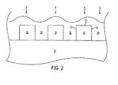
- a first mask pattern comprising spaced apart portions 10 is formed over a target layer 11.
- Target layer 11 can be any of various layers formed during conventional semiconductor fabrication techniques to be etched, such as a conductive or semiconductor layer wherein gate electrodes are formed.
- the first mask pattern typically comprises an organic material, such as a photoresist material, and can contain a component which is capable of causing a reaction, such as a cross-linking reaction, in a subsequently applied layer.
- first mask pattern 10 comprises a photoresist material capable of generating an acid.
- Suitable materials include a mixture of a novolac resin, a napthoquinonediazde-based photo-sensitive agent, and a cholo-methyl-triazine functioning as an acid generator.
- Some embodiments of the present invention also include forming the first mask pattern from a mixture comprising a poly-hydroxy-styrene derivative and an onium salt which functions as a photo-assisted acid generator.
- the first mask layer can be formed of a chemically amplified resist which employs a mechanism of producing an acid when is exposed to certain types of radiation, such as UV rays, an electron beam or X-rays, or when heated.
- layer 20 is deposited covering the first mask pattern 10.
- layer 20 comprises a material capable of undergoing a cross-linking reaction, such as a material capable of undergoing a cross-linking reaction in the presence of an acid.
- Suitable materials for layer 20 include water-soluble and water-insoluble resins, water-soluble and water-insoluble resins which cause a cross-linking reaction in the presence of an acid, water-soluble and water-insoluble cross-linking agents, and mixtures thereof.
- a water-soluble resin is selected from the group consisting of a polyacrylic acid, polyvinyl acetal, polyvinylpyrrolidone, polyvinyl alcohol, polyethyleneimine, styrene-maleic anhydride copolymer, polyvinylamine, polyallylamine, oxazoline group-containing water-soluble resins, water-soluble urethane, water-soluble phenol, water-soluble epoxy, water-soluble melamine resins, water-soluble urea resins, alkyd resins, sulfonamide, a salt thereof, and a mixture of two or more thereof.
- the water-soluble cross-linking agent can be one type of material or two or more types of materials selected from the group consisting of melamine-based cross-linking agents such as melamine derivatives or methyl-lolmelamine derivatives, urea-based cross-linking agents such as urea derivatives, methyloy urea derivatives, ethylene urea carboxylates, or methylol-ethylene-urea derivatives; and amino-based cross-linking agents such as benzoguanamine, gylcoluril, isocyanates.
- melamine-based cross-linking agents such as melamine derivatives or methyl-lolmelamine derivatives
- urea-based cross-linking agents such as urea derivatives, methyloy urea derivatives, ethylene urea carboxylates, or methylol-ethylene-urea derivatives
- amino-based cross-linking agents such as benzoguanamine, gylcoluril, isocyanates.
- the second layer 20 is formed of a polyvinyl acetal resin, and the amount thereof controlled by controlling the extent of acetalization of the polyvinyl acetal resin.
- layer 20 can comprise a material selected from a group of a mixture of polyvinyl acetal and methoxy-methylol-urea, a mixture of polyvinylyl acetal and methoxy-methylol-melamine, or a mixture of methyoxy-methylol-melamine and polyallyl-amine.
- a cross-linker such as JSR CSX004, distributed by JSR Micro, Inc., Sunnyvale, CA. JSR CSX0004 is only slightly soluble in water.
- the second layer 20 is deposited using a solvent which is incapable of dissolving the first resist pattern 10.
- Suitable solvents for depositing layer 20 include pure water or a mixture of pure water and an alcohol.
- a species capable of reacting or causing a cross-linking reaction with layer 20 is generated in the first mask pattern.
- Suitable treatments include irradiation with light having an appropriate wavelength, as illustrated by arrows A ( Fig. 2 ), over the entire exposed surface.
- portions of first mask layer 10 can be selectively irradiated, as by shielding other portions, to generate an acid in selected portions 10 of the first mask pattern.
- laser thermal annealing can be performed to heat selected portions 10 of the first mask pattern to generate an acid. In cases where only certain portions 10 of the first mask pattern are selectively heated or treated, the cross-linked spacer layer would be formed only on the selectively heated or treated portions.
- portions of layer 20 are caused to undergo a reaction to form a spacer over the first mask pattern.
- the wafer can be baked, as by heating to a temperature of about 60° to about 130°, thereby permitting an acid generated in first mask pattern to diffuse to second layer 20 causing a cross-linking reaction to form a cross-linked spacer on the first mask pattern.
- the cross-linked spacer comprises an upper portion 30 formed on the upper surfaces 12 of the first mask pattern 10 and side portions 31 formed on side surfaces 13 of first mask pattern 10.
- the amount of heating can be controlled by controlling the duration of heating, such as 60 seconds to 120 seconds, depending upon the particular material involved and the required thickness of the cross-linked spacer.
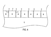
- an upper portion of layer 20 and the upper portion 30 of the cross-linked spacer are removed.
- Such removal can be effected by either by chemical removal or CMP.
- CMP can be advantageously omitted, and the upper portions of layer 20 and upper portions 30 of the cross-linked spacer are removed by etching, as by selectively etching the upper portion of layer 20 followed by selectively etching to remove upper portion 30 of the cross-linked spacer.
- a timed etching technique can be employed to remove, separately or in one step, the upper portion of layer 20 and upper portion 30 of the cross-linked spacer to expose the upper surfaces 12 of portions 10 of the first mask pattern, as shown in Fig. 4 .
- Suitable etchants to remove the upper portion of (uncross-linked) cross-linkable layer 20 and upper portions 30 of the cross-linked spacer include a gas etchant composition comprising, and O 2 , N 2 , and C x H y F z .
- the remaining portion of (uncross-linked) cross-linkable layer 20 together with portions 10 of the first mask pattern are removed, as by etching, to form a second or final mask pattern comprising cross-linked portions 31 previously on side surfaces 13 of portions 10 of the first mask pattern.
- Suitable etchants to remove remaining uncross-linked layer 20 and portions 10 include gas etchant composition comprising O 2 , N 2 , and C x H y F z .
- etching is conducted, using the second mask pattern, to form features 60 in target layer 11, such as gate electrodes.
- Features 60 are self-aligned with cross-linked spacer portions 31 and have a width similar to the thickness of spacer layer 31.
- the present invention can be implemented using various types of materials and techniques.
- an acid can be generated by the methods, and employing the materials, disclosed in U.S. Patent No. 5,858,620 and in U.S. Patent No. 6,319,853 .
- prebaking may be performed after forming the first mask pattern and after depositing layer 20.
- An acid can be formed by means other than by irradiation, as by treating the first mask pattern with an acidic solution prior to depositing layer 20, and subsequently, heating to permit the acid to diffuse and cross-link a portion of layer 20.
- Embodiments of the present invention advantageously employ organic materials for the first mask pattern and layer 20, thereby minimizing transportation among different tools. Further, in embodiments of the present invention, problematic CMP of an insulating layer can be avoided by etching, as by employing a timed etching technique. Examples of the present invention can be implemented using a single exposure step in forming the first mask pattern, thereby avoiding misalignment issues attendant upon a multiple exposures with intervening processing.
- the present invention can be employed in the fabrication of semiconductor chips comprising any of various types of semiconductor devices, including semiconductor memory devices, such as eraseable, programmable, read-only memories (EPROMs), electrically eraseable programmable read-only memories (EEPROMs), and flash eraseable programmable read-only memories (FEPROMs).
- semiconductor memory devices such as eraseable, programmable, read-only memories (EPROMs), electrically eraseable programmable read-only memories (EEPROMs), and flash eraseable programmable read-only memories (FEPROMs).
- semiconductor memory devices such as eraseable, programmable, read-only memories (EPROMs), electrically eraseable programmable read-only memories (EEPROMs), and flash eraseable programmable read-only memories (FEPROMs).
- EPROMs eraseable, programmable, read-only memories
- EEPROMs electrically eraseable programmable read-only memories
- FEPROMs flash eraseable programmable read-only memories
- the present invention enables the efficient fabrication of semiconductor chips comprising devices with accurate ultrafine design features with high manufacturing throughput.
- the present invention enjoys industrial applicability in fabricating semiconductor chips useful in any of various types of industrial applications, including chips having highly integrated semiconductor devices, including flash memory semiconductor devices exhibiting increased circuit speed.
Landscapes
- Physics & Mathematics (AREA)
- Engineering & Computer Science (AREA)
- General Physics & Mathematics (AREA)
- Condensed Matter Physics & Semiconductors (AREA)
- Manufacturing & Machinery (AREA)
- Computer Hardware Design (AREA)
- Microelectronics & Electronic Packaging (AREA)
- Power Engineering (AREA)
- Exposure And Positioning Against Photoresist Photosensitive Materials (AREA)
- Photosensitive Polymer And Photoresist Processing (AREA)
- Exposure Of Semiconductors, Excluding Electron Or Ion Beam Exposure (AREA)
Applications Claiming Priority (2)
| Application Number | Priority Date | Filing Date | Title |
|---|---|---|---|
| US11/775,727 US8642474B2 (en) | 2007-07-10 | 2007-07-10 | Spacer lithography |
| PCT/US2008/008470 WO2009009095A1 (en) | 2007-07-10 | 2008-07-10 | Spacer lithography |
Publications (2)
| Publication Number | Publication Date |
|---|---|
| EP2168008A1 EP2168008A1 (en) | 2010-03-31 |
| EP2168008B1 true EP2168008B1 (en) | 2014-11-26 |
Family
ID=39765015
Family Applications (1)
| Application Number | Title | Priority Date | Filing Date |
|---|---|---|---|
| EP08780091.8A Active EP2168008B1 (en) | 2007-07-10 | 2008-07-10 | Spacer lithography |
Country Status (7)
Families Citing this family (11)
| Publication number | Priority date | Publication date | Assignee | Title |
|---|---|---|---|---|
| CN101937838B (zh) * | 2009-06-26 | 2012-10-03 | 罗门哈斯电子材料有限公司 | 形成电子器件的方法 |
| EP2287667B1 (en) | 2009-06-26 | 2013-03-27 | Rohm and Haas Electronic Materials, L.L.C. | Self-aligned spacer multiple patterning methods |
| JP5753351B2 (ja) * | 2009-11-19 | 2015-07-22 | ローム アンド ハース エレクトロニック マテリアルズ エルエルシーRohm and Haas Electronic Materials LLC | 電子デバイスを形成する方法 |
| US8815747B2 (en) | 2010-06-03 | 2014-08-26 | Micron Technology, Inc. | Methods of forming patterns on substrates |
| US9233840B2 (en) * | 2010-10-28 | 2016-01-12 | International Business Machines Corporation | Method for improving self-assembled polymer features |
| US9330914B2 (en) | 2013-10-08 | 2016-05-03 | Micron Technology, Inc. | Methods of forming line patterns in substrates |
| JP6126570B2 (ja) * | 2013-12-13 | 2017-05-10 | 富士フイルム株式会社 | パターン形成方法、電子デバイスの製造方法 |
| US9257439B2 (en) | 2014-02-27 | 2016-02-09 | Taiwan Semiconductor Manufacturing Company, Ltd. | Structure and method for FinFET SRAM |
| CN110391133B (zh) * | 2018-04-17 | 2021-07-20 | 联华电子股份有限公司 | 图案化方法 |
| US11069692B2 (en) | 2018-07-31 | 2021-07-20 | Taiwan Semiconductor Manufacturing Co., Ltd. | FinFET SRAM cells with dielectric fins |
| US11437385B2 (en) | 2018-09-24 | 2022-09-06 | Taiwan Semiconductor Manufacturing Co., Ltd. | FinFET SRAM cells with reduced fin pitch |
Family Cites Families (62)
| Publication number | Priority date | Publication date | Assignee | Title |
|---|---|---|---|---|
| DE3242113A1 (de) * | 1982-11-13 | 1984-05-24 | Ibm Deutschland Gmbh, 7000 Stuttgart | Verfahren zur herstellung einer duennen dielektrischen isolation in einem siliciumhalbleiterkoerper |
| JPS62199068A (ja) * | 1986-02-27 | 1987-09-02 | Toshiba Corp | 半導体装置及びその製造方法 |
| DE3682395D1 (de) * | 1986-03-27 | 1991-12-12 | Ibm | Verfahren zur herstellung von seitenstrukturen. |
| US5322764A (en) * | 1991-05-21 | 1994-06-21 | Mitsubishi Denki Kabushiki Kaisha | Method for forming a patterned resist |
| US5654202A (en) * | 1992-03-24 | 1997-08-05 | Eastman Kodak Company | Stabilization of a patterned planarizing layer for solid state imagers prior to color filter pattern formation |
| US5618383A (en) * | 1994-03-30 | 1997-04-08 | Texas Instruments Incorporated | Narrow lateral dimensioned microelectronic structures and method of forming the same |
| JP3317582B2 (ja) * | 1994-06-01 | 2002-08-26 | 菱電セミコンダクタシステムエンジニアリング株式会社 | 微細パターンの形成方法 |
| JPH08152716A (ja) * | 1994-11-28 | 1996-06-11 | Mitsubishi Electric Corp | ネガ型レジスト及びレジストパターンの形成方法 |
| JPH08321613A (ja) * | 1995-05-26 | 1996-12-03 | Ricoh Co Ltd | 半導体装置の製造方法 |
| US5795830A (en) * | 1995-06-06 | 1998-08-18 | International Business Machines Corporation | Reducing pitch with continuously adjustable line and space dimensions |
| US5879955A (en) * | 1995-06-07 | 1999-03-09 | Micron Technology, Inc. | Method for fabricating an array of ultra-small pores for chalcogenide memory cells |
| TW329539B (en) * | 1996-07-05 | 1998-04-11 | Mitsubishi Electric Corp | The semiconductor device and its manufacturing method |
| TW353775B (en) * | 1996-11-27 | 1999-03-01 | Tokyo Electron Ltd | Production of semiconductor device |
| TW372337B (en) * | 1997-03-31 | 1999-10-21 | Mitsubishi Electric Corp | Material for forming micropattern and manufacturing method of semiconductor using the material and semiconductor apparatus |
| TW383416B (en) * | 1997-06-26 | 2000-03-01 | Matsushita Electric Ind Co Ltd | Pattern forming method |
| US6063688A (en) * | 1997-09-29 | 2000-05-16 | Intel Corporation | Fabrication of deep submicron structures and quantum wire transistors using hard-mask transistor width definition |
| JP3189773B2 (ja) * | 1998-01-09 | 2001-07-16 | 三菱電機株式会社 | レジストパターン形成方法及びこれを用いた半導体装置の製造方法並びに半導体装置 |
| US6331378B1 (en) * | 1998-02-25 | 2001-12-18 | Matsushita Electric Industrial Co., Ltd. | Pattern forming method |
| US6183938B1 (en) * | 1998-12-08 | 2001-02-06 | Advanced Micro Devices, Inc. | Conformal organic coatings for sidewall patterning of sublithographic structures |
| US6291137B1 (en) * | 1999-01-20 | 2001-09-18 | Advanced Micro Devices, Inc. | Sidewall formation for sidewall patterning of sub 100 nm structures |
| US6335531B1 (en) * | 1999-04-06 | 2002-01-01 | Micron Technology, Inc. | Modification of resist and/or resist processing with fluorescence detection |
| JP3950584B2 (ja) * | 1999-06-29 | 2007-08-01 | Azエレクトロニックマテリアルズ株式会社 | 水溶性樹脂組成物 |
| JP2001066782A (ja) * | 1999-08-26 | 2001-03-16 | Mitsubishi Electric Corp | 半導体装置の製造方法並びに半導体装置 |
| JP2001100428A (ja) * | 1999-09-27 | 2001-04-13 | Mitsubishi Electric Corp | 半導体装置の製造方法、微細パターン形成用薬液および半導体装置 |
| US6239008B1 (en) * | 1999-09-29 | 2001-05-29 | Advanced Micro Devices, Inc. | Method of making a density multiplier for semiconductor device manufacturing |
| US6362057B1 (en) * | 1999-10-26 | 2002-03-26 | Motorola, Inc. | Method for forming a semiconductor device |
| JP2001284813A (ja) * | 2000-03-31 | 2001-10-12 | Mitsubishi Electric Corp | 多層配線板の製造方法 |
| JP3343341B2 (ja) * | 2000-04-28 | 2002-11-11 | ティーディーケイ株式会社 | 微細パターン形成方法及びそれに用いる現像/洗浄装置、及びそれを用いためっき方法、及びそれを用いた薄膜磁気ヘッドの製造方法 |
| US6492075B1 (en) * | 2000-06-16 | 2002-12-10 | Advanced Micro Devices, Inc. | Chemical trim process |
| US6534243B1 (en) * | 2000-10-23 | 2003-03-18 | Advanced Micro Devices, Inc. | Chemical feature doubling process |
| US6383952B1 (en) | 2001-02-28 | 2002-05-07 | Advanced Micro Devices, Inc. | RELACS process to double the frequency or pitch of small feature formation |
| JP3633595B2 (ja) * | 2001-08-10 | 2005-03-30 | 富士通株式会社 | レジストパターン膨潤化材料およびそれを用いた微小パターンの形成方法および半導体装置の製造方法 |
| US7189783B2 (en) * | 2001-11-27 | 2007-03-13 | Fujitsu Limited | Resist pattern thickening material, resist pattern and forming process thereof, and semiconductor device and manufacturing process thereof |
| US6638441B2 (en) * | 2002-01-07 | 2003-10-28 | Macronix International Co., Ltd. | Method for pitch reduction |
| US6862798B2 (en) * | 2002-01-18 | 2005-03-08 | Hitachi Global Storage Technologies Netherlands B.V. | Method of making a narrow pole tip by ion beam deposition |
| JP3953822B2 (ja) * | 2002-01-25 | 2007-08-08 | 富士通株式会社 | レジストパターン薄肉化材料、レジストパターン及びその製造方法、並びに、半導体装置及びその製造方法 |
| JP2004056000A (ja) * | 2002-07-23 | 2004-02-19 | Renesas Technology Corp | レジストパターン形成方法およびその方法を用いた半導体デバイスの製造方法 |
| JP3850767B2 (ja) * | 2002-07-25 | 2006-11-29 | 富士通株式会社 | レジストパターン厚肉化材料、レジストパターン及びその製造方法、並びに、半導体装置及びその製造方法 |
| US6566280B1 (en) * | 2002-08-26 | 2003-05-20 | Intel Corporation | Forming polymer features on a substrate |
| KR100493029B1 (ko) * | 2002-10-26 | 2005-06-07 | 삼성전자주식회사 | 반도체 소자의 미세 패턴 형성방법 |
| JP4191506B2 (ja) * | 2003-02-21 | 2008-12-03 | Tdk株式会社 | 高密度インダクタおよびその製造方法 |
| US6905975B2 (en) * | 2003-07-03 | 2005-06-14 | Micron Technology, Inc. | Methods of forming patterned compositions |
| JP3774713B2 (ja) * | 2003-10-15 | 2006-05-17 | 株式会社東芝 | コンタクトホールの形成方法 |
| JP4143023B2 (ja) * | 2003-11-21 | 2008-09-03 | 株式会社東芝 | パターン形成方法および半導体装置の製造方法 |
| US7498225B1 (en) * | 2003-12-04 | 2009-03-03 | Advanced Micro Devices, Inc. | Systems and methods for forming multiple fin structures using metal-induced-crystallization |
| US7314691B2 (en) * | 2004-04-08 | 2008-01-01 | Samsung Electronics Co., Ltd. | Mask pattern for semiconductor device fabrication, method of forming the same, method for preparing coating composition for fine pattern formation, and method of fabricating semiconductor device |
| JP4490228B2 (ja) * | 2004-06-15 | 2010-06-23 | 富士通株式会社 | レジストパターン厚肉化材料、レジストパターンの形成方法、半導体装置及びその製造方法 |
| US7655387B2 (en) * | 2004-09-02 | 2010-02-02 | Micron Technology, Inc. | Method to align mask patterns |
| JP4302065B2 (ja) * | 2005-01-31 | 2009-07-22 | 株式会社東芝 | パターン形成方法 |
| JP4676325B2 (ja) * | 2005-02-18 | 2011-04-27 | 富士通株式会社 | レジストパターン厚肉化材料、レジストパターンの形成方法、半導体装置及びその製造方法 |
| GB2423634A (en) * | 2005-02-25 | 2006-08-30 | Seiko Epson Corp | A patterning method for manufacturing high resolution structures |
| US7429536B2 (en) * | 2005-05-23 | 2008-09-30 | Micron Technology, Inc. | Methods for forming arrays of small, closely spaced features |
| US7396781B2 (en) * | 2005-06-09 | 2008-07-08 | Micron Technology, Inc. | Method and apparatus for adjusting feature size and position |
| GB2429332A (en) * | 2005-08-18 | 2007-02-21 | Filtronic Compound Semiconduct | A method of producing a trench with a coating of a cross linked polymer |
| US8153350B2 (en) * | 2005-08-24 | 2012-04-10 | Taiwan Semiconductor Manufacturing Co., Ltd. | Method and material for forming high etch resistant double exposure patterns |
| JP4566862B2 (ja) * | 2005-08-25 | 2010-10-20 | 富士通株式会社 | レジストパターン厚肉化材料、レジストパターンの形成方法、半導体装置及びその製造方法 |
| JP5177948B2 (ja) * | 2005-10-11 | 2013-04-10 | 東京エレクトロン株式会社 | レジスト膜の除去方法およびコンピュータ読取可能な記憶媒体 |
| JP2007140151A (ja) * | 2005-11-18 | 2007-06-07 | Renesas Technology Corp | 微細パターン形成用材料、微細パターン形成方法、それを用いた電子デバイスの製造方法、およびそれにより製造された電子デバイス |
| JP4719069B2 (ja) * | 2006-04-21 | 2011-07-06 | パナソニック株式会社 | レジスト材料及びそれを用いたパターン形成方法 |
| US7488685B2 (en) * | 2006-04-25 | 2009-02-10 | Micron Technology, Inc. | Process for improving critical dimension uniformity of integrated circuit arrays |
| US7959818B2 (en) * | 2006-09-12 | 2011-06-14 | Hynix Semiconductor Inc. | Method for forming a fine pattern of a semiconductor device |
| US7790357B2 (en) * | 2006-09-12 | 2010-09-07 | Hynix Semiconductor Inc. | Method of forming fine pattern of semiconductor device |
-
2007
- 2007-07-10 US US11/775,727 patent/US8642474B2/en active Active
-
2008
- 2008-07-08 TW TW097125658A patent/TWI431665B/zh active
- 2008-07-10 JP JP2010516054A patent/JP5120983B2/ja active Active
- 2008-07-10 EP EP08780091.8A patent/EP2168008B1/en active Active
- 2008-07-10 CN CN2008800237522A patent/CN101730864B/zh active Active
- 2008-07-10 KR KR1020107002932A patent/KR101520440B1/ko active Active
- 2008-07-10 WO PCT/US2008/008470 patent/WO2009009095A1/en active Application Filing
Also Published As
| Publication number | Publication date |
|---|---|
| JP2010534346A (ja) | 2010-11-04 |
| KR20100057799A (ko) | 2010-06-01 |
| JP5120983B2 (ja) | 2013-01-16 |
| CN101730864A (zh) | 2010-06-09 |
| US8642474B2 (en) | 2014-02-04 |
| US20090017628A1 (en) | 2009-01-15 |
| TWI431665B (zh) | 2014-03-21 |
| TW200915389A (en) | 2009-04-01 |
| WO2009009095A1 (en) | 2009-01-15 |
| KR101520440B1 (ko) | 2015-05-15 |
| EP2168008A1 (en) | 2010-03-31 |
| CN101730864B (zh) | 2012-07-18 |
Similar Documents
| Publication | Publication Date | Title |
|---|---|---|
| EP2168008B1 (en) | Spacer lithography | |
| KR100865104B1 (ko) | 레지스트 패턴 후육화 재료, 및 레지스트 패턴의 형성 방법 | |
| US8940475B2 (en) | Double patterning with inline critical dimension slimming | |
| JP5851052B2 (ja) | パターン平滑化及びインライン限界寸法のスリム化のための蒸気処理プロセス | |
| US8158332B2 (en) | Method of manufacturing a semiconductor device | |
| US10317801B2 (en) | Method for forming photolithographic pattern | |
| JPH11160890A (ja) | フォトレジストの制御された収縮 | |
| CN109427553A (zh) | 保护晶圆免受斜面污染的半导体方法 | |
| US20120193763A1 (en) | Method of manufacturing semiconductor device, semiconductor device and resist coater | |
| JP4566862B2 (ja) | レジストパターン厚肉化材料、レジストパターンの形成方法、半導体装置及びその製造方法 | |
| CN103280403A (zh) | 双栅氧器件的制造方法 | |
| JP4413880B2 (ja) | 半導体装置の製造方法 | |
| US6635409B1 (en) | Method of strengthening photoresist to prevent pattern collapse | |
| US20040038549A1 (en) | Semiconductor apparatus fabrication method | |
| US6635585B1 (en) | Method for forming patterned polyimide layer | |
| US20060088784A1 (en) | Effective photoresist stripping process for high dosage and high energy ion implantation | |
| US6989333B2 (en) | Process for forming a pattern | |
| US9086631B2 (en) | EUV resist sensitivity reduction | |
| TWI707199B (zh) | 使層圖樣化之方法 | |
| US6642152B1 (en) | Method for ultra thin resist linewidth reduction using implantation | |
| JP5332107B2 (ja) | レジストパターン形成方法および半導体装置の製造方法 | |
| JP2013164628A (ja) | レジストパターン形成方法および半導体装置の製造方法 | |
| US20100248498A1 (en) | Material stripping in semiconductor devices by evaporation | |
| US20100119982A1 (en) | Etching method and manufacturing method of semiconductor device |
Legal Events
| Date | Code | Title | Description |
|---|---|---|---|
| PUAI | Public reference made under article 153(3) epc to a published international application that has entered the european phase |
Free format text: ORIGINAL CODE: 0009012 |
|
| 17P | Request for examination filed |
Effective date: 20100118 |
|
| AK | Designated contracting states |
Kind code of ref document: A1 Designated state(s): AT BE BG CH CY CZ DE DK EE ES FI FR GB GR HR HU IE IS IT LI LT LU LV MC MT NL NO PL PT RO SE SI SK TR |
|
| AX | Request for extension of the european patent |
Extension state: AL BA MK RS |
|
| DAX | Request for extension of the european patent (deleted) | ||
| 17Q | First examination report despatched |
Effective date: 20110301 |
|
| GRAP | Despatch of communication of intention to grant a patent |
Free format text: ORIGINAL CODE: EPIDOSNIGR1 |
|
| INTG | Intention to grant announced |
Effective date: 20140718 |
|
| GRAS | Grant fee paid |
Free format text: ORIGINAL CODE: EPIDOSNIGR3 |
|
| GRAA | (expected) grant |
Free format text: ORIGINAL CODE: 0009210 |
|
| AK | Designated contracting states |
Kind code of ref document: B1 Designated state(s): AT BE BG CH CY CZ DE DK EE ES FI FR GB GR HR HU IE IS IT LI LT LU LV MC MT NL NO PL PT RO SE SI SK TR |
|
| REG | Reference to a national code |
Ref country code: GB Ref legal event code: FG4D |
|
| REG | Reference to a national code |
Ref country code: CH Ref legal event code: EP |
|
| REG | Reference to a national code |
Ref country code: DE Ref legal event code: R082 Ref document number: 602008035592 Country of ref document: DE |
|
| REG | Reference to a national code |
Ref country code: AT Ref legal event code: REF Ref document number: 698528 Country of ref document: AT Kind code of ref document: T Effective date: 20141215 |
|
| REG | Reference to a national code |
Ref country code: IE Ref legal event code: FG4D |
|
| REG | Reference to a national code |
Ref country code: DE Ref legal event code: R096 Ref document number: 602008035592 Country of ref document: DE Effective date: 20150108 |
|
| REG | Reference to a national code |
Ref country code: NL Ref legal event code: VDEP Effective date: 20141126 |
|
| REG | Reference to a national code |
Ref country code: AT Ref legal event code: MK05 Ref document number: 698528 Country of ref document: AT Kind code of ref document: T Effective date: 20141126 |
|
| REG | Reference to a national code |
Ref country code: LT Ref legal event code: MG4D |
|
| PG25 | Lapsed in a contracting state [announced via postgrant information from national office to epo] |
Ref country code: PT Free format text: LAPSE BECAUSE OF FAILURE TO SUBMIT A TRANSLATION OF THE DESCRIPTION OR TO PAY THE FEE WITHIN THE PRESCRIBED TIME-LIMIT Effective date: 20150326 Ref country code: IS Free format text: LAPSE BECAUSE OF FAILURE TO SUBMIT A TRANSLATION OF THE DESCRIPTION OR TO PAY THE FEE WITHIN THE PRESCRIBED TIME-LIMIT Effective date: 20150326 Ref country code: NL Free format text: LAPSE BECAUSE OF FAILURE TO SUBMIT A TRANSLATION OF THE DESCRIPTION OR TO PAY THE FEE WITHIN THE PRESCRIBED TIME-LIMIT Effective date: 20141126 Ref country code: LT Free format text: LAPSE BECAUSE OF FAILURE TO SUBMIT A TRANSLATION OF THE DESCRIPTION OR TO PAY THE FEE WITHIN THE PRESCRIBED TIME-LIMIT Effective date: 20141126 Ref country code: NO Free format text: LAPSE BECAUSE OF FAILURE TO SUBMIT A TRANSLATION OF THE DESCRIPTION OR TO PAY THE FEE WITHIN THE PRESCRIBED TIME-LIMIT Effective date: 20150226 Ref country code: FI Free format text: LAPSE BECAUSE OF FAILURE TO SUBMIT A TRANSLATION OF THE DESCRIPTION OR TO PAY THE FEE WITHIN THE PRESCRIBED TIME-LIMIT Effective date: 20141126 Ref country code: ES Free format text: LAPSE BECAUSE OF FAILURE TO SUBMIT A TRANSLATION OF THE DESCRIPTION OR TO PAY THE FEE WITHIN THE PRESCRIBED TIME-LIMIT Effective date: 20141126 |
|
| PG25 | Lapsed in a contracting state [announced via postgrant information from national office to epo] |
Ref country code: AT Free format text: LAPSE BECAUSE OF FAILURE TO SUBMIT A TRANSLATION OF THE DESCRIPTION OR TO PAY THE FEE WITHIN THE PRESCRIBED TIME-LIMIT Effective date: 20141126 Ref country code: LV Free format text: LAPSE BECAUSE OF FAILURE TO SUBMIT A TRANSLATION OF THE DESCRIPTION OR TO PAY THE FEE WITHIN THE PRESCRIBED TIME-LIMIT Effective date: 20141126 Ref country code: HR Free format text: LAPSE BECAUSE OF FAILURE TO SUBMIT A TRANSLATION OF THE DESCRIPTION OR TO PAY THE FEE WITHIN THE PRESCRIBED TIME-LIMIT Effective date: 20141126 Ref country code: SE Free format text: LAPSE BECAUSE OF FAILURE TO SUBMIT A TRANSLATION OF THE DESCRIPTION OR TO PAY THE FEE WITHIN THE PRESCRIBED TIME-LIMIT Effective date: 20141126 Ref country code: GR Free format text: LAPSE BECAUSE OF FAILURE TO SUBMIT A TRANSLATION OF THE DESCRIPTION OR TO PAY THE FEE WITHIN THE PRESCRIBED TIME-LIMIT Effective date: 20150227 Ref country code: CY Free format text: LAPSE BECAUSE OF FAILURE TO SUBMIT A TRANSLATION OF THE DESCRIPTION OR TO PAY THE FEE WITHIN THE PRESCRIBED TIME-LIMIT Effective date: 20141126 |
|
| PG25 | Lapsed in a contracting state [announced via postgrant information from national office to epo] |
Ref country code: DK Free format text: LAPSE BECAUSE OF FAILURE TO SUBMIT A TRANSLATION OF THE DESCRIPTION OR TO PAY THE FEE WITHIN THE PRESCRIBED TIME-LIMIT Effective date: 20141126 Ref country code: EE Free format text: LAPSE BECAUSE OF FAILURE TO SUBMIT A TRANSLATION OF THE DESCRIPTION OR TO PAY THE FEE WITHIN THE PRESCRIBED TIME-LIMIT Effective date: 20141126 Ref country code: RO Free format text: LAPSE BECAUSE OF FAILURE TO SUBMIT A TRANSLATION OF THE DESCRIPTION OR TO PAY THE FEE WITHIN THE PRESCRIBED TIME-LIMIT Effective date: 20141126 Ref country code: CZ Free format text: LAPSE BECAUSE OF FAILURE TO SUBMIT A TRANSLATION OF THE DESCRIPTION OR TO PAY THE FEE WITHIN THE PRESCRIBED TIME-LIMIT Effective date: 20141126 Ref country code: SK Free format text: LAPSE BECAUSE OF FAILURE TO SUBMIT A TRANSLATION OF THE DESCRIPTION OR TO PAY THE FEE WITHIN THE PRESCRIBED TIME-LIMIT Effective date: 20141126 |
|
| REG | Reference to a national code |
Ref country code: DE Ref legal event code: R097 Ref document number: 602008035592 Country of ref document: DE |
|
| PG25 | Lapsed in a contracting state [announced via postgrant information from national office to epo] |
Ref country code: PL Free format text: LAPSE BECAUSE OF FAILURE TO SUBMIT A TRANSLATION OF THE DESCRIPTION OR TO PAY THE FEE WITHIN THE PRESCRIBED TIME-LIMIT Effective date: 20141126 |
|
| PLBE | No opposition filed within time limit |
Free format text: ORIGINAL CODE: 0009261 |
|
| STAA | Information on the status of an ep patent application or granted ep patent |
Free format text: STATUS: NO OPPOSITION FILED WITHIN TIME LIMIT |
|
| 26N | No opposition filed |
Effective date: 20150827 |
|
| PG25 | Lapsed in a contracting state [announced via postgrant information from national office to epo] |
Ref country code: IT Free format text: LAPSE BECAUSE OF FAILURE TO SUBMIT A TRANSLATION OF THE DESCRIPTION OR TO PAY THE FEE WITHIN THE PRESCRIBED TIME-LIMIT Effective date: 20141126 |
|
| PG25 | Lapsed in a contracting state [announced via postgrant information from national office to epo] |
Ref country code: MC Free format text: LAPSE BECAUSE OF FAILURE TO SUBMIT A TRANSLATION OF THE DESCRIPTION OR TO PAY THE FEE WITHIN THE PRESCRIBED TIME-LIMIT Effective date: 20141126 Ref country code: SI Free format text: LAPSE BECAUSE OF FAILURE TO SUBMIT A TRANSLATION OF THE DESCRIPTION OR TO PAY THE FEE WITHIN THE PRESCRIBED TIME-LIMIT Effective date: 20141126 |
|
| REG | Reference to a national code |
Ref country code: CH Ref legal event code: PL |
|
| PG25 | Lapsed in a contracting state [announced via postgrant information from national office to epo] |
Ref country code: LU Free format text: LAPSE BECAUSE OF FAILURE TO SUBMIT A TRANSLATION OF THE DESCRIPTION OR TO PAY THE FEE WITHIN THE PRESCRIBED TIME-LIMIT Effective date: 20150710 |
|
| REG | Reference to a national code |
Ref country code: IE Ref legal event code: MM4A |
|
| PG25 | Lapsed in a contracting state [announced via postgrant information from national office to epo] |
Ref country code: CH Free format text: LAPSE BECAUSE OF NON-PAYMENT OF DUE FEES Effective date: 20150731 Ref country code: LI Free format text: LAPSE BECAUSE OF NON-PAYMENT OF DUE FEES Effective date: 20150731 |
|
| REG | Reference to a national code |
Ref country code: FR Ref legal event code: ST Effective date: 20160331 |
|
| PG25 | Lapsed in a contracting state [announced via postgrant information from national office to epo] |
Ref country code: FR Free format text: LAPSE BECAUSE OF NON-PAYMENT OF DUE FEES Effective date: 20150731 |
|
| PG25 | Lapsed in a contracting state [announced via postgrant information from national office to epo] |
Ref country code: IE Free format text: LAPSE BECAUSE OF NON-PAYMENT OF DUE FEES Effective date: 20150710 |
|
| PG25 | Lapsed in a contracting state [announced via postgrant information from national office to epo] |
Ref country code: MT Free format text: LAPSE BECAUSE OF FAILURE TO SUBMIT A TRANSLATION OF THE DESCRIPTION OR TO PAY THE FEE WITHIN THE PRESCRIBED TIME-LIMIT Effective date: 20141126 |
|
| PG25 | Lapsed in a contracting state [announced via postgrant information from national office to epo] |
Ref country code: BG Free format text: LAPSE BECAUSE OF FAILURE TO SUBMIT A TRANSLATION OF THE DESCRIPTION OR TO PAY THE FEE WITHIN THE PRESCRIBED TIME-LIMIT Effective date: 20141126 Ref country code: HU Free format text: LAPSE BECAUSE OF FAILURE TO SUBMIT A TRANSLATION OF THE DESCRIPTION OR TO PAY THE FEE WITHIN THE PRESCRIBED TIME-LIMIT; INVALID AB INITIO Effective date: 20080710 |
|
| PG25 | Lapsed in a contracting state [announced via postgrant information from national office to epo] |
Ref country code: TR Free format text: LAPSE BECAUSE OF FAILURE TO SUBMIT A TRANSLATION OF THE DESCRIPTION OR TO PAY THE FEE WITHIN THE PRESCRIBED TIME-LIMIT Effective date: 20141126 |
|
| PG25 | Lapsed in a contracting state [announced via postgrant information from national office to epo] |
Ref country code: BE Free format text: LAPSE BECAUSE OF FAILURE TO SUBMIT A TRANSLATION OF THE DESCRIPTION OR TO PAY THE FEE WITHIN THE PRESCRIBED TIME-LIMIT Effective date: 20141126 |
|
| P01 | Opt-out of the competence of the unified patent court (upc) registered |
Effective date: 20230530 |
|
| PGFP | Annual fee paid to national office [announced via postgrant information from national office to epo] |
Ref country code: DE Payment date: 20240717 Year of fee payment: 17 |
|
| PGFP | Annual fee paid to national office [announced via postgrant information from national office to epo] |
Ref country code: GB Payment date: 20240724 Year of fee payment: 17 |