EP2132550B1 - Procédé de fabrication d'un échantillon pour la microscopie électronique - Google Patents
Procédé de fabrication d'un échantillon pour la microscopie électronique Download PDFInfo
- Publication number
- EP2132550B1 EP2132550B1 EP08748344A EP08748344A EP2132550B1 EP 2132550 B1 EP2132550 B1 EP 2132550B1 EP 08748344 A EP08748344 A EP 08748344A EP 08748344 A EP08748344 A EP 08748344A EP 2132550 B1 EP2132550 B1 EP 2132550B1
- Authority
- EP
- European Patent Office
- Prior art keywords
- sample
- ion beams
- ion
- plane
- range
- Prior art date
- Legal status (The legal status is an assumption and is not a legal conclusion. Google has not performed a legal analysis and makes no representation as to the accuracy of the status listed.)
- Active
Links
- 238000000034 method Methods 0.000 title claims description 73
- 238000001493 electron microscopy Methods 0.000 title claims description 6
- 238000004519 manufacturing process Methods 0.000 title claims description 4
- 238000010884 ion-beam technique Methods 0.000 claims description 123
- 238000005530 etching Methods 0.000 claims description 49
- 239000000463 material Substances 0.000 claims description 11
- 239000007787 solid Substances 0.000 claims description 2
- 230000000284 resting effect Effects 0.000 claims 1
- 239000000523 sample Substances 0.000 description 113
- 150000002500 ions Chemical group 0.000 description 18
- 238000002360 preparation method Methods 0.000 description 11
- 238000005520 cutting process Methods 0.000 description 8
- 239000000835 fiber Substances 0.000 description 5
- 238000000992 sputter etching Methods 0.000 description 4
- XKRFYHLGVUSROY-UHFFFAOYSA-N Argon Chemical compound [Ar] XKRFYHLGVUSROY-UHFFFAOYSA-N 0.000 description 2
- 238000002679 ablation Methods 0.000 description 2
- 230000005540 biological transmission Effects 0.000 description 2
- 230000001419 dependent effect Effects 0.000 description 2
- 238000004377 microelectronic Methods 0.000 description 2
- 239000000853 adhesive Substances 0.000 description 1
- 230000001070 adhesive effect Effects 0.000 description 1
- 229910052786 argon Inorganic materials 0.000 description 1
- 230000015572 biosynthetic process Effects 0.000 description 1
- 238000000576 coating method Methods 0.000 description 1
- 229910003460 diamond Inorganic materials 0.000 description 1
- 239000010432 diamond Substances 0.000 description 1
- 230000000694 effects Effects 0.000 description 1
- 238000000605 extraction Methods 0.000 description 1
- 230000002349 favourable effect Effects 0.000 description 1
- 238000010304 firing Methods 0.000 description 1
- 230000010355 oscillation Effects 0.000 description 1
- 230000003534 oscillatory effect Effects 0.000 description 1
- 238000009304 pastoral farming Methods 0.000 description 1
- 238000004886 process control Methods 0.000 description 1
- 239000004065 semiconductor Substances 0.000 description 1
- 229910000679 solder Inorganic materials 0.000 description 1
- 239000011343 solid material Substances 0.000 description 1
- 238000004544 sputter deposition Methods 0.000 description 1
- 239000000126 substance Substances 0.000 description 1
- 230000008542 thermal sensitivity Effects 0.000 description 1
- 230000005641 tunneling Effects 0.000 description 1
- 238000003631 wet chemical etching Methods 0.000 description 1
Images


Classifications
-
- G—PHYSICS
- G01—MEASURING; TESTING
- G01N—INVESTIGATING OR ANALYSING MATERIALS BY DETERMINING THEIR CHEMICAL OR PHYSICAL PROPERTIES
- G01N1/00—Sampling; Preparing specimens for investigation
- G01N1/28—Preparing specimens for investigation including physical details of (bio-)chemical methods covered elsewhere, e.g. G01N33/50, C12Q
- G01N1/32—Polishing; Etching
-
- H—ELECTRICITY
- H01—ELECTRIC ELEMENTS
- H01J—ELECTRIC DISCHARGE TUBES OR DISCHARGE LAMPS
- H01J2237/00—Discharge tubes exposing object to beam, e.g. for analysis treatment, etching, imaging
- H01J2237/30—Electron or ion beam tubes for processing objects
- H01J2237/317—Processing objects on a microscale
- H01J2237/3174—Etching microareas
- H01J2237/31745—Etching microareas for preparing specimen to be viewed in microscopes or analyzed in microanalysers
Definitions
- the invention relates to a method for producing a sample for electron microscopy, which is cut from a solid material according to the preamble of claim 1.
- Samples for electron microscopy can be prepared in a variety of ways. In order to be able to view samples with an electron microscope, they must be correspondingly processed by exposing the observation surface to be observed by means of an etching process. By scanning electron microscopic (SEM) observation, the desired surface is observed. When viewing the sample with a transmission electron microscope (TEM), the sample is thinned by the etching such that they can be irradiated by the electrons in the TEM and the sample can be viewed in transmission. The quality of the image resolution is very much dependent on the quality of the sample. For this, the sample should be uniformly adjusted to a corresponding desired surface area for the SEM method or to a desired defined thickness for the TEM method by a suitably suitable etching process.
- SEM scanning electron microscopic
- the sample structure is not changed by the process itself during this etching process.
- a piece of the material to be examined is mechanically sawn out of the sample body and then treated by etching in order to subsequently examine the sample with a SEM or TEM.
- the wet-chemical etching method is not effective in this respect.
- the samples are processed with an ion beam by ion etching such as sputter etching in a vacuum.
- the ion beam for example, an argon ion beam having a diameter of about 1 mm is used.
- Samples for electron microscopy can now be prepared in various ways. In particular, three methods are known today for processing samples with ion beam etching.
- Ion beam slope etching is a technique that has long been used to produce SEM cross-section samples.
- a part of the sample surface is covered with a mask.
- the uncovered part of the surface is ion etched until a kind of embankment is created.
- the achieved cutting depths are in the range of a few 2.0 ⁇ m to a maximum of 50 ⁇ m .
- the preparation times vary from a few minutes to several hours, depending on the material and the depth of the etching.
- the sample In order to obtain a uniform cut surface, the sample must oscillate during the etching. This is especially true for structured materials with very different sputtering rates, as they occur in the semiconductor industry.
- the currently known methods and techniques for making a slope cut use only a single ion source or ion beam.
- Drahtabschattungssupervised The method of wire shading is used for the production of TEM samples with extremely large electron-transparent areas (several mm long) (Patent EP 1 505 383 A1 ).
- a thin wire or a fiber is glued to the surface of the sample to be etched and bombarded with a conventional ion source perpendicular to the surface.
- the shading of the wire creates a wedge-shaped sample which is electron-transparent at the thinnest point.
- the thickness of the samples is previously mechanically reduced to about 100 microns.
- the sample oscillates during the etching process. Also in this process, the requirements go in the direction of high etch depths at the same time low etching time and excellent sample quality.
- TEM standard preparation Another well-known and widespread preparation method is the TEM standard preparation.
- a mechanically prepared specimen about 3 mm in diameter and about 20 to 50 ⁇ m in thickness is made either with two ion sources from one sample side, or one ion source on each side of the specimen, than on the front and back etched on the rear side at the same time.
- the sample rotates or oscillates to avoid etch structures.
- the ion beam may be moved relative to the sample, or both.
- the requirements in the direction of high etching depth with low etching time and excellent sample quality are not, or only with great effort to realize.
- the patent US 6,914,244 relates to an ion beam etching system for producing samples for electron microscopy after the wire shading method.
- two ion sources are used whose ion beams are guided onto the sample to be etched.
- the use of two ion sources should increase the removal rate.
- the sample is moved in rotation with respect to the ion beams, whereby the ion beams can also be moved.
- the patent US 5,009,743 describes an ion beam etching system with two ion sources, the rays of which are guided at a very shallow angle of 0 to 10 degrees onto the sample surface, the ion sources being arranged symmetrically with respect to the sample and facing each other. It is also disclosed that one ion beam may be directed from the underside and the other from the top to the sample for double-sided ablation of the sample.
- the invention has for its object to eliminate the disadvantages of the prior art.
- an etching method is to be realized which enables high depths of cut with a short preparation time, with which a high degree of cost-effectiveness can be achieved with high reliability and good achievable sample quality.
- electron microscopic samples are etched with at least three fixedly arranged ion beams which are directed at an angle onto the sample surface and meet there.
- the samples are also not moved in this case, so that there is no relative movement between the ion beams and the sample, with which the entire arrangement is operated stationarily arranged.
- a solid state material cut for example mechanically.
- An additional chemical and / or mechanical treatment is possible: Thereafter, a sample surface formed on the sample is treated with an ion beam at a predetermined angle of incidence so that material is removed from the sample surface by ion etching up to the sample, in the region of the impact zone of the ion beam, the desired observation surface is exposed, which then allows viewing in the desired region of the sample with an electron microscope, wherein at least three fixed ion beams are guided at a predetermined angle aligned with each other on the sample surface, so that the ion beams at least touch or cut on the sample surface and There form an impact zone, and that both the sample, as well as the ion beams are not moved and thus operated stationary.
- the present etching method makes it possible to observe the quiescent sample during the etching process in high resolution with an observation means and thus to control the process, preferably with a light microscope or a scanning electron microscope. This observation should be made at least temporarily over the course of the entire etching process.
- the sample is advantageously aligned with the observation means prior to ion etching and is not moved during the etching process.
- the sample can additionally be cooled during the etching process, in particular in order to be able to allow even higher beam powers, which in the sequence allow even higher etching speeds, even with very sensitive samples.
- the conditions for this can be optimally selected and set at the arrangement, for example by the choice of the angle between the ion beams, the angle of incidence of the ion beams on the sample surface, same or different energy of the beams, beam diameter, beam current density and position of the beams in the impact area of the sample.
- the values can be predetermined, adjusted or varied individually and / or in combination. Also, the values may be varied or tracked according to a predetermined program, for example with an automated control, depending on the progress of the etching process.
- At least three fixed ion beams are used for a TEM sample, these need not lie in one plane.
- favorable results are achieved even with three fixed ion beams.
- Three or more ion beams produce even better results, and it is advantageous if these three or more ion beams are guided in a single plane to the sample.
- the ion beams may be generated for each beam with its own ion source, or it may be advantageous to generate at least two ion beams with a single ion source by extraction from a common source array, such as a plasma.
- three ion sources are arranged at an angle of 60 ° to each other.
- the ion beams form an intersection that can be directed to a selected point or landing area on the sample surface.
- the rays form a circular sector of 60 ° to 120 °.
- the beams have to be different Make directions on the sample surface, so that an angle of 0 ° to 180 °, preferably 20 ° to 160 ° with respect to the sample surface is formed, depending on the application, (etch depth or ⁇ tzumble) and that an intersection of the individual beams on a selectable impact zone on the sample arises.
- the circular sector can be formed by two or more beams. This can be realized by multiple ion beams extracted from one or more ion sources.
- the angle of the circular sector influences the cutting speed or surface quality.
- three ion sources each offset by 60 ° and forming a circular sector are used.
- the angle size different results can be achieved and thus adjusted as desired.
- the ion energy of the beams is in the range of 200 eV to 12 keV, preferably in the range of 500 eV to 8 keV.
- the ion energy of the single sources can be varied to achieve certain etch profiles.
- the above-mentioned bombardment sector is formed, which makes a rotation of the sample unnecessary to avoid preferential directions.
- the position of the cutting area can be adjusted, or even controlled, even during the etching process. As a result, the influence of the profile of the single beam is lower and the method is less critical in the settings, which increases the reliability.
- Ion energy and current density can also be selected, for example, depending on the thermal sensitivity of the sample.
- the presented method thus enables a targeted adjustability of important parameters high degree of process control flexibility, making it easy to adapt to a wide range of samples with high process productivity.
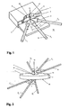
- a flat specimen 1 is cut, for example with a diamond tool from the material to be examined and mechanically polished on both sides.
- the sample 1 then has two sides with the two surfaces 3a and 3b and the thickness d, as shown in FIG FIG. 2 is shown.
- This is a typical sample, as is customary for TEM observations with the observation direction 12 of the electron microscope and also treated according to the TEM standard etching method with only one ion beam at which the sample 1 or the ion beam is moved.
- the sample surface 3 is then etched on one side or on both sides 3a, 3b simultaneously with at least three ion beams J 1 , J 2 , J ' 1 , J' 2 , which touch or overlap in the impact zone 4 of the sample surface 3.
- the arrangement is operated stationary, it is thus neither the sample 1 nor the ion beams J moved relative to each other. Even better results are achieved if at least three ion beams J 1 , J 2 , J 3 are used and they all touch and / or overlap in the impact zone 4.
- the three ion beams J are guided at an angle ⁇ onto the sample surface 3. These thus form a kind of circle segment and span a plane 10. For example, if three ion beams J to J 3 are used at the mutually-facing angles ⁇ , ⁇ ', ⁇ ", they may be located in a single plane 10 (FIG. Fig.
- ion beams J can also be positioned inside the cone ( Fig. 6 ).
- the cone tip in which the ion beams J are all brought together lies in each case in the area of The plane 10 and / or the cone 11 with its center axis Z, Z 'may be aligned perpendicular to the sample surface 3 or tilted at an angle ⁇ relative to the normal N of the sample surface 3, such as this also in the Figures 5 and 6 is shown schematically.
- the etching process can be ended and the sample 1 with the TEM in the observation direction 12 can be viewed in high resolution.
- the observation direction 12 leads to the observation surface 20 which is identical to the etched sample surface 3 and thus to the impact zone 4 'of the ion beams J at the end of the etching process.
- FIG. 1 An arrangement with a sample 1 is schematically for the slope etching method in FIG FIG. 1 shown.
- the present method is particularly well suited for the more complex and delicate slope etching process.
- the sample 1 is cut out of the material to be examined.
- a planar mask 2 is brought to a selected sample surface 3, the surface of which is advantageously arranged perpendicular to the sample surface.
- the mask is arranged slightly spaced from the sample surface 3, which adjoins at a distance in the range of 10 .mu.m to 100 .mu.m and thereby form the two surfaces in this area an adjacent line.
- the impingement zone 4 of the at least three, preferably three, ion beams J 1 , J 2 , with their beam diameter q, is placed.
- the ion beams J lie in a plane 10 and the plane passes through this line.
- This plane 10 with the ion beams is advantageously positioned perpendicular to the sample surface 3 and may be parallel to the surface of the mask 2.
- the plane 10 may also be slightly tilted relative to the surface of the mask 2 by an angle in the range of 0 ° to 10 °, preferably from 0 ° to 5 °.
- the material is preferably removed from the sample 1 in the direction of the ion beams J, whereby a kind of trench is formed with the now deeper impingement zone 4 '.
- the impact zone 4, 4 'thus shifts, depending on the progress of the etching process.
- Laterally to the plane 10 and thus laterally to the ion beams within the sample 1 is also easily etched by grazing or scattering ions and there is a so-called slope 5 at the desired location to be considered which forms the observation surface 20 shown.
- the observation direction 12 for the SEM is aligned, with advantage, perpendicular to the lateral sample surface and in particular to the observation surface 20.
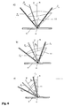
- the ion beams J are all aligned in a plane 10. These can enclose different angles ⁇ , ⁇ ', ⁇ "and thus form a kind of circle segment
- the clamped circle segment advantageously includes an angle ⁇ which lies in the range of 10 ° to 180 °, preferably in the range of 30 ° to 140 °
- there are also other ion beams within the circle segment which is closed by the two ion beams which enclose the largest angle and bound the circle segment
- the ion beams can be symmetrical or asymmetrical be aligned to a vertical N to the sample surface, as shown schematically in the FIGS. 5a to 5c is shown.
- the circular segment thus formed with the central axis Z can also be tilted in relation to this vertical N by an angle ⁇ for further adjustment of desired etching conditions.
- the angle ⁇ is advantageously in the range of ⁇ 20 °, preferably in the range of ⁇ 10 °.
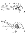
- FIGS. 3 and 4 there is shown an arrangement according to the wire shading method, which is also a preferred preparation for the present method.
- the figures show two different views in which the sample 1 is shown slightly rotated for clarity.
- this sample 1 often has a structured surface 3, which may additionally contain coatings or layer systems (not shown).
- a wire or a fiber 7 with a small predetermined diameter is fixed on the sample surface 3, for example with an adhesive. It is customary to choose a sample width d of about 100 ⁇ m or less to 10 ⁇ m the fiber to be applied is smaller in diameter than the sample width d and forms a mask.
- at least three, preferably three, ion beams J, preferably perpendicular to the sample surface 3, are then directed onto the fiber 7 where the impact zone 4 is then located. In this case, the vertical N lies within the plane 10.
- the plane 10 is placed parallel to the direction of the wire or even passes through the wire axis.
- the sample 1 is etched so strongly by the ion beams J that there is a clear wedge-shaped formation transverse to its length l.
- the etched flanks 6 on both sides of the sample 1 now enclose an elongated comb which tapers and is electron-permeable in this region for a TEM observation which takes place from the side of the sample, preferably in the vertical direction of observation 12, with an arrow transverse to the sample longitudinal direction is shown.
- the fiber 2 is also strongly etched in this state.
- the ion beams form a kind of circle segment within the plane 10 and the ion beams can impinge on the sample surface 3 at different angles or be tilted as a whole.
- the clamped-on circular segment advantageously includes an angle .alpha. Which is in the range of 10.degree. To 180.degree., Preferably in the range of 30.degree. To 140.degree., And all ion beams lie in the plane 10 of this circular segment spanned by the latter. Depending on the number is, preferably in the range of 30 ° to 140 ° and all the ion beams are in the plane spanned by this plane 10 of this circle segment.
- there are also other ion beams within the circle segment which is terminated by the two ion beams, which enclose the aforementioned largest angle and bound the circle segment.
- the ion beams may be oriented symmetrically or asymmetrically to a perpendicular N to the sample surface, as shown schematically in FIGS FIGS. 5a to 5c is shown.
- the circular segment thus formed with the central axis Z can also be tilted in relation to this vertical N by an angle ⁇ for further adjustment of desired etching conditions.
- the angle ⁇ is advantageously chosen to be in the range of ⁇ 20 °, preferably in the range of ⁇ 10 °.
- FIGS. 5a to 5b are various possible positions and directions of incidence of ion beams J, which are guided in a common plane (10) lying opposite to the sample surface, shown schematically.
- FIG. 5a is located by the two ion beams J 1 , J 2 at the angle ⁇ limited circle segment with its central axis of symmetry Z on the vertical N to the sample surface 3 on which the impingement zone 4 is for all ion beams J and in which these are brought together in a kind of intersection.
- the two ion beams J 1 , J 2 are guided with respect to the central axis Z and the vertical N by the angle ⁇ / 2 in the direction of the impact zone.
- the circular segment with the central axis Z can be tilted with respect to the vertical N by an angle ⁇ , ie have a corresponding asymmetry, as shown in the FIG. 5b is shown.
- a tilt in which all ion beams come to lie on one side of the vertical N is in FIG. 5c
- the three ion beams J1-J3 are guided at corresponding angles ⁇ lying on a conical surface 11 whose tip is in the impact zone 4 lies, as in the FIGS. 6a to 6c is shown.
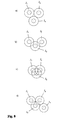
- FIGS. 7a to 7d Different combinations of the at least three ion beams J in the area of the impact zone 4 are in the FIGS. 7a to 7d shown in supervision.
- the ion beams with their cross-section q are all in the same plane 10 and touch each other in the impact zone at least as shown in FIG Figure 7a , These are all in a line within the plane 10 which intersects the impact zone 4. They can overlap individually according to FIG. 7b or all overlap according to FIG. 7c or touch and overlap according to FIG. 7d ,
- FIGS. 8a to 8d The merging of at least three ion beams J within an impingement zone 4 for ion beams J which lie on at least one conical surface and / or also in between is in the FIGS. 8a to 8d shown.
- FIG. 8a shows three contacting ion beams J 1 to J 3 in the impingement zone 4.
- Three partially overlapping ion beams are in FIG. 8b shown.
- Three overlapping ion beams are in FIG. 8c shown and four ion beams overlapping and touching in the FIG. 8d ,
Claims (15)
- Procédé de fabrication d'un échantillon (1) pour la microscopie électronique, dans lequel ledit échantillon est coupé dans un matériau solide et comprend une face d'échantillon (3) que l'on traite à l'aide d'un faisceau ionique (J) sous un angle d'incidence prédéfini, de manière à obtenir un enlèvement de matériau par décapage de la face d'échantillon (3) jusqu'à ce que soit dégagée sur ledit échantillon (1), au niveau de la zone d'impact (4) du faisceau ionique (J), la surface d'observation (20) souhaitée qui permet l'observation (12) au microscope électronique dans la zone souhaitée de l'échantillon (1), caractérisé par le fait qu'au moins trois faisceaux ioniques (J1, J2, J3) fixes, orientés entre eux selon un angle (α) donné, sont dirigés sur la face d'échantillon (3), de sorte telle que les faisceaux ioniques (J1, J2, J3) se coupent, ou au moins se touchent, au niveau de ladite face d'échantillon (3), en formant à cet endroit une zone d'impact (4), et par le fait que l'échantillon (1) et les faisceaux ioniques (J1, J2, J3) restent immobiles et sont donc exploités en régime stationnaire.
- Procédé conforme à la revendication 1, caractérisé par le fait que l'échantillon (1) est traité avec les faisceaux ioniques (J1, J2, J3) selon la méthode du décapage ionique.
- Procédé conforme à la revendication 1 , caractérisé par le fait que l'échantillon (1) est traité avec les faisceaux ioniques (J1, J2, J3) selon la méthode de la projection d'ombre.
- Procédé conforme à la revendication 1 , caractérisé par le fait qu'un échantillon TEM standard (1) est traité avec les faisceaux ioniques (J1, J2) en dirigeant lesdits faisceaux - au nombre d'au moins trois - sur au moins l'une des faces (3a, 3b) de l'échantillon, afin d'en enlever la surface (3a, 3b).
- Procédé conforme à l'une quelconque des revendications précédentes, caractérisé par le fait qu'une pluralité de faisceaux ioniques (J1, J2) fixes, de préférence au nombre de trois, sont dirigés selon différents angles (α,α',α") sur la face d'échantillon (3), pour le moins en se touchant tous dans la zone d'impact (4) ou, de préférence, en se superposant au moins pour partie.
- Procédé conforme à l'une quelconque des revendications précédentes, caractérisé par le fait que la position réciproque des faisceaux ioniques (J1, J2) dans la zone d'impact (4) et, par conséquent, leur degré de superposition, est réglable pour au moins l'un des faisceaux, de préférence au cours du décapage.
- Procédé conforme à l'une quelconque des revendications précédentes, caractérisé par le fait que deux au moins des faisceaux ioniques (J1, J2) sont produits ensemble par une seule source d'ions.
- Procédé conforme à l'une quelconque des revendications précédentes, caractérisé par le fait que deux au moins des faisceaux ioniques (J1, J2) sont produits chacun par une source d'ions séparée.
- Procédé conforme à l'une quelconque des revendications précédentes, caractérisé par le fait que l'échantillon (1) au repos est observé en haute résolution durant le décapage ionique, au moins par intermittence, à l'aide d'un moyen d'observation, de préférence un microscope optique ou un microscope électronique à balayage.
- Procédé conforme à la revendication 2, caractérisé- par l'utilisation, lors du décapage ionique, d'un cache (2) doté d'une surface plane qui vient s'abouter contre la face d'échantillon (3) à une distance comprise entre 10 µm et 100 µm, de telle sorte que les deux faces forment dans ce secteur une ligne de jonction au niveau de laquelle est située la zone d'impact (4) des faisceaux ioniques (J1, J2, J3),- par le fait que les faisceaux ioniques décrivent un plan (10) dans lequel est située ladite ligne de jonction, ledit plan (10) étant légèrement incliné par rapport à la surface du cache (2), selon un angle compris entre 0° et 10°, de préférence entre 0° et 5°- et par le fait que la surface du cache (2) est disposée, de préférence, perpendiculairement à la face d'échantillon (3).
- Procédé conforme à la revendication 2 ou 10, caractérisé par le fait que les faisceaux ioniques (J1, J2, J3) décrivent un segment de cercle avec un angle (α) compris entre 10° et 180°, de préférence entre 30° et 140°, et par le fait que tous les faisceaux ioniques (J1, J2, J3) sont situés dans le plan dudit segment de cercle.
- Procédé conforme à la revendication 3, caractérisé par le fait qu'avec la méthode de la projection d'ombre, les faisceaux ioniques (J1, J2, J3) sont dirigés dans un plan (10) parallèle au fil (7), plan dans lequel se situe également la ligne (N) perpendiculaire à la face d'échantillon (3).
- Procédé conforme à la revendication 3 ou 12, caractérisé par le fait que le plan (10) décrit par les faisceaux ioniques (J) est disposé de telle sorte, par rapport à la perpendiculaire (N), que les deux forment un angle β de l'ordre de ± 20°, de préférence de l'ordre de ± 10°.
- Procédé conforme à la revendication 3 ou 12, caractérisé par le fait que les faisceaux ioniques (J1, J2, J3) décrivent un segment de cercle avec un angle (α) compris entre 10° et 180°, de préférence entre 30° et 140°, et par le fait que tous les faisceaux ioniques sont situés dans le plan dudit segment de cercle, deux d'entre eux (J1, J2)) étant positionnés, de préférence, symétriquement à la normale (N) de la surface.
- Procédé conforme à la revendication 4, caractérisé par le fait que les faisceaux ioniques (J1, J2, J3) sont orientés, au moins sur l'une des faces de l'échantillon (1), de telle sorte qu'ils s'inscrivent dans une aire latérale de cône et par le fait que les faisceaux sont réunis à la pointe dudit cône, en atteignant la zone d'impact (4) au moins sur cette seule face d'échantillon.
Applications Claiming Priority (2)
| Application Number | Priority Date | Filing Date | Title |
|---|---|---|---|
| CH3582007 | 2007-03-06 | ||
| PCT/CH2008/000085 WO2008106815A2 (fr) | 2007-03-06 | 2008-03-03 | Procédé de fabrication d'un échantillon pour la microscopie électronique |
Publications (2)
| Publication Number | Publication Date |
|---|---|
| EP2132550A2 EP2132550A2 (fr) | 2009-12-16 |
| EP2132550B1 true EP2132550B1 (fr) | 2012-11-07 |
Family
ID=38042823
Family Applications (1)
| Application Number | Title | Priority Date | Filing Date |
|---|---|---|---|
| EP08748344A Active EP2132550B1 (fr) | 2007-03-06 | 2008-03-03 | Procédé de fabrication d'un échantillon pour la microscopie électronique |
Country Status (4)
| Country | Link |
|---|---|
| US (1) | US8168960B2 (fr) |
| EP (1) | EP2132550B1 (fr) |
| JP (1) | JP5249955B2 (fr) |
| WO (1) | WO2008106815A2 (fr) |
Families Citing this family (13)
| Publication number | Priority date | Publication date | Assignee | Title |
|---|---|---|---|---|
| GB201002645D0 (en) * | 2010-02-17 | 2010-03-31 | Univ Lancaster | Method and apparatus for ion beam polishing |
| AT509608B1 (de) | 2010-12-23 | 2011-10-15 | Leica Mikrosysteme Gmbh | Vorrichtung und verfahren zur kühlung von proben während einer einer ionenstrahlpräparation |
| AT510606B1 (de) | 2011-02-09 | 2012-05-15 | Leica Mikrosysteme Gmbh | Vorrichtung und verfahren zur probenpräparation |
| DE102011111190A1 (de) * | 2011-08-25 | 2013-02-28 | Fraunhofer-Gesellschaft zur Förderung der angewandten Forschung e.V. | Verfahren und Vorrichtung zur Präparation einer Probe für die Mikrostrukturdiagnostik |
| JP2013243307A (ja) * | 2012-05-22 | 2013-12-05 | Toshiba Corp | 半導体製造装置および半導体装置の製造方法 |
| DE102013012225A1 (de) * | 2013-07-23 | 2015-01-29 | Carl Zeiss Microscopy Gmbh | Verfahren zur TEM-Lamellen-Herstellung und Anordnung für TEM-Lamellen-Schutzvorrichtung |
| CN103792123B (zh) * | 2014-02-25 | 2016-01-27 | 山西太钢不锈钢股份有限公司 | 一种透射电子显微镜观察用钢铁样品的制备方法 |
| US9911573B2 (en) | 2014-03-09 | 2018-03-06 | Ib Labs, Inc. | Methods, apparatuses, systems and software for treatment of a specimen by ion-milling |
| US10354836B2 (en) * | 2014-03-09 | 2019-07-16 | Ib Labs, Inc. | Methods, apparatuses, systems and software for treatment of a specimen by ion-milling |
| DE102015219298B4 (de) * | 2015-10-06 | 2019-01-24 | Fraunhofer-Gesellschaft zur Förderung der angewandten Forschung e.V. | Verfahren zur Präparation einer Probe für die Mikrostrukturdiagnostik sowie Probe für die Mikrostrukturdiagnostik |
| CN105699149A (zh) * | 2016-04-05 | 2016-06-22 | 工业和信息化部电子第五研究所 | 芯片失效分析过程中的剥层方法 |
| US10417881B2 (en) * | 2016-05-02 | 2019-09-17 | Norman R. Byrne | Wireless status indicator light |
| US20230352263A1 (en) * | 2020-01-29 | 2023-11-02 | Hitachi High-Tech Corporation | Ion milling device |
Family Cites Families (15)
| Publication number | Priority date | Publication date | Assignee | Title |
|---|---|---|---|---|
| JPS6064228A (ja) * | 1983-09-20 | 1985-04-12 | Nec Corp | 透過型電子顕微鏡試料の作製方法及びその作製装置 |
| US5009743A (en) * | 1989-11-06 | 1991-04-23 | Gatan Incorporated | Chemically-assisted ion beam milling system for the preparation of transmission electron microscope specimens |
| US5825035A (en) * | 1993-03-10 | 1998-10-20 | Hitachi, Ltd. | Processing method and apparatus using focused ion beam generating means |
| JPH0817800A (ja) * | 1994-06-29 | 1996-01-19 | Hitachi Ltd | 集束イオンビーム装置およびそれを用いた試料加工方法 |
| US5472566A (en) * | 1994-11-14 | 1995-12-05 | Gatan, Inc. | Specimen holder and apparatus for two-sided ion milling system |
| DE29507225U1 (de) * | 1995-04-29 | 1995-07-13 | Gruenewald Wolfgang Dr Rer Nat | Ionenstrahlpräparationsvorrichtung für die Elektronenmikroskopie |
| JP2001077058A (ja) * | 1999-09-08 | 2001-03-23 | Seiko Instruments Inc | 集束イオンビームを用いた加工方法 |
| US6768110B2 (en) * | 2000-06-21 | 2004-07-27 | Gatan, Inc. | Ion beam milling system and method for electron microscopy specimen preparation |
| JP4178741B2 (ja) * | 2000-11-02 | 2008-11-12 | 株式会社日立製作所 | 荷電粒子線装置および試料作製装置 |
| US7053370B2 (en) * | 2001-10-05 | 2006-05-30 | Canon Kabushiki Kaisha | Information acquisition apparatus, cross section evaluating apparatus, cross section evaluating method, and cross section working apparatus |
| US7002152B2 (en) * | 2003-02-15 | 2006-02-21 | Bal-Tec Ag | Sample preparation for transmission electron microscopy |
| US20040222082A1 (en) * | 2003-05-05 | 2004-11-11 | Applied Materials, Inc. | Oblique ion milling of via metallization |
| US6784427B1 (en) * | 2003-07-31 | 2004-08-31 | Bal-Tec Ag | Samples for transmission electron microscopy |
| ATE459091T1 (de) * | 2004-07-01 | 2010-03-15 | Fei Co | Methode zum entfernen einer mikroskopischen probe von einem substrat |
| JP4878135B2 (ja) * | 2005-08-31 | 2012-02-15 | エスアイアイ・ナノテクノロジー株式会社 | 荷電粒子ビーム装置及び試料加工方法 |
-
2008
- 2008-03-03 JP JP2009552039A patent/JP5249955B2/ja active Active
- 2008-03-03 WO PCT/CH2008/000085 patent/WO2008106815A2/fr active Application Filing
- 2008-03-03 US US12/529,849 patent/US8168960B2/en active Active
- 2008-03-03 EP EP08748344A patent/EP2132550B1/fr active Active
Also Published As
| Publication number | Publication date |
|---|---|
| WO2008106815A2 (fr) | 2008-09-12 |
| US8168960B2 (en) | 2012-05-01 |
| WO2008106815A3 (fr) | 2008-10-23 |
| JP5249955B2 (ja) | 2013-07-31 |
| US20100025577A1 (en) | 2010-02-04 |
| JP2010520465A (ja) | 2010-06-10 |
| EP2132550A2 (fr) | 2009-12-16 |
Similar Documents
| Publication | Publication Date | Title |
|---|---|---|
| EP2132550B1 (fr) | Procédé de fabrication d'un échantillon pour la microscopie électronique | |
| DE602006000278T2 (de) | Mehrmaliges Rundfräsen zur Probenherstellung | |
| DE4226694C2 (de) | Verfahren zum Separieren eines kleinen Abschnittes einer Probe | |
| DE102005040267B4 (de) | Verfahren zum Herstellen einer mehrschichtigen elektrostatischen Linsenanordnung, insbesondere einer Phasenplatte und derartige Phasenplatte | |
| EP0048291B1 (fr) | Structure comprenant un corps de silicium présentant une ouverture le traversant de part en part et procédé de fabrication | |
| EP1447656A1 (fr) | Echantillons pour microscope électronique à transmission | |
| DE602005000352T2 (de) | Methode zur Entnahme einer mikroskopischen Probe von einem Substrat | |
| EP1665320B1 (fr) | Procede de preparation d'un echantillon pour examens au microscope electronique, et porte-echantillon et support de transport utilises a cet effet | |
| DE10329383B4 (de) | Ionenstrahldetektor für Ionenimplantationsanlagen, Faraday-Behälter dafür und Verfahren zur Steuerung der Eigenschaften eines Ionenstrahls mittels des Ionenstrahldetektors | |
| WO2008071303A2 (fr) | Installation optique à particules | |
| DE102010024625A1 (de) | Verfahren zum Bearbeiten eines Objekts | |
| DE102011002583B4 (de) | Teilchenstrahlgerät und Verfahren zur Bearbeitung und/oder Analyse einer Probe | |
| DE102006007431B4 (de) | Durch Halbleitersilizium-Verfahrenstechnik gebildeter Probenträger sowie Verfahren zur Herstellung | |
| EP2504725A1 (fr) | Procédé et dispositif pour fabriquer une plaque à zones de fresnel | |
| EP3153838B1 (fr) | Procédé de préparation d'un échantillon pour le diagnostic de microstructure et échantillon pour le diagnostic de microstructure | |
| DE112014003194T5 (de) | Verfahren zu Bearbeitung einer Probe in einem mindestens zwei Partikelstrahlen erzeugenden Gerät und Gerät zur Durchführung des Verfahrens | |
| DE102013102537B4 (de) | Proben-vorbereitungsverfahren | |
| DE10393678B4 (de) | Verfahren zum Bilden einer Schicht auf einem Substrat | |
| DE102004001173B4 (de) | Verfahren zur Herstellung von zur Untersuchung mittels Transmissionselektronenmikroskopie geeigneten Proben | |
| DE102010041156B4 (de) | Blendeneinheit für ein Teilchenstrahlgerät sowie Teilchenstrahlgerät | |
| WO2014173999A1 (fr) | Procédé de séparation individuelle de puces à partir d'une plaquette | |
| DE60127383T2 (de) | Behandlungsmethode für eine diamantoberfläche und entsprechende oberfläche | |
| DE102012022168A1 (de) | Verfahren zum bearbeiten eines materialstücks | |
| WO2018083322A1 (fr) | Dispositif d'extraction de porteurs de charge électrique d'un espace de production de porteurs de charge électrique | |
| WO2016110505A2 (fr) | Dispositif d'extraction de porteurs de charge électrique d'un espace de génération de porteurs de charge et procédé pour faire fonctionner un tel dispositif |
Legal Events
| Date | Code | Title | Description |
|---|---|---|---|
| PUAI | Public reference made under article 153(3) epc to a published international application that has entered the european phase |
Free format text: ORIGINAL CODE: 0009012 |
|
| 17P | Request for examination filed |
Effective date: 20091006 |
|
| AK | Designated contracting states |
Kind code of ref document: A2 Designated state(s): AT BE BG CH CY CZ DE DK EE ES FI FR GB GR HR HU IE IS IT LI LT LU LV MC MT NL NO PL PT RO SE SI SK TR |
|
| RIN1 | Information on inventor provided before grant (corrected) |
Inventor name: GABATHULER, ALEXANDER Inventor name: GRUENEWALD, WOLFGANG Inventor name: VOGT, ALEX |
|
| 17Q | First examination report despatched |
Effective date: 20120308 |
|
| GRAP | Despatch of communication of intention to grant a patent |
Free format text: ORIGINAL CODE: EPIDOSNIGR1 |
|
| DAX | Request for extension of the european patent (deleted) | ||
| GRAS | Grant fee paid |
Free format text: ORIGINAL CODE: EPIDOSNIGR3 |
|
| GRAA | (expected) grant |
Free format text: ORIGINAL CODE: 0009210 |
|
| AK | Designated contracting states |
Kind code of ref document: B1 Designated state(s): AT BE BG CH CY CZ DE DK EE ES FI FR GB GR HR HU IE IS IT LI LT LU LV MC MT NL NO PL PT RO SE SI SK TR |
|
| REG | Reference to a national code |
Ref country code: GB Ref legal event code: FG4D Free format text: NOT ENGLISH |
|
| REG | Reference to a national code |
Ref country code: CH Ref legal event code: EP Ref country code: AT Ref legal event code: REF Ref document number: 583198 Country of ref document: AT Kind code of ref document: T Effective date: 20121115 |
|
| REG | Reference to a national code |
Ref country code: IE Ref legal event code: FG4D Free format text: LANGUAGE OF EP DOCUMENT: GERMAN |
|
| REG | Reference to a national code |
Ref country code: DE Ref legal event code: R096 Ref document number: 502008008604 Country of ref document: DE Effective date: 20130103 |
|
| REG | Reference to a national code |
Ref country code: NL Ref legal event code: VDEP Effective date: 20121107 |
|
| REG | Reference to a national code |
Ref country code: LT Ref legal event code: MG4D |
|
| PG25 | Lapsed in a contracting state [announced via postgrant information from national office to epo] |
Ref country code: ES Free format text: LAPSE BECAUSE OF FAILURE TO SUBMIT A TRANSLATION OF THE DESCRIPTION OR TO PAY THE FEE WITHIN THE PRESCRIBED TIME-LIMIT Effective date: 20130218 Ref country code: NL Free format text: LAPSE BECAUSE OF FAILURE TO SUBMIT A TRANSLATION OF THE DESCRIPTION OR TO PAY THE FEE WITHIN THE PRESCRIBED TIME-LIMIT Effective date: 20121107 Ref country code: FI Free format text: LAPSE BECAUSE OF FAILURE TO SUBMIT A TRANSLATION OF THE DESCRIPTION OR TO PAY THE FEE WITHIN THE PRESCRIBED TIME-LIMIT Effective date: 20121107 Ref country code: HR Free format text: LAPSE BECAUSE OF FAILURE TO SUBMIT A TRANSLATION OF THE DESCRIPTION OR TO PAY THE FEE WITHIN THE PRESCRIBED TIME-LIMIT Effective date: 20121107 Ref country code: NO Free format text: LAPSE BECAUSE OF FAILURE TO SUBMIT A TRANSLATION OF THE DESCRIPTION OR TO PAY THE FEE WITHIN THE PRESCRIBED TIME-LIMIT Effective date: 20130207 Ref country code: SE Free format text: LAPSE BECAUSE OF FAILURE TO SUBMIT A TRANSLATION OF THE DESCRIPTION OR TO PAY THE FEE WITHIN THE PRESCRIBED TIME-LIMIT Effective date: 20121107 Ref country code: LT Free format text: LAPSE BECAUSE OF FAILURE TO SUBMIT A TRANSLATION OF THE DESCRIPTION OR TO PAY THE FEE WITHIN THE PRESCRIBED TIME-LIMIT Effective date: 20121107 Ref country code: IS Free format text: LAPSE BECAUSE OF FAILURE TO SUBMIT A TRANSLATION OF THE DESCRIPTION OR TO PAY THE FEE WITHIN THE PRESCRIBED TIME-LIMIT Effective date: 20130307 |
|
| PG25 | Lapsed in a contracting state [announced via postgrant information from national office to epo] |
Ref country code: PL Free format text: LAPSE BECAUSE OF FAILURE TO SUBMIT A TRANSLATION OF THE DESCRIPTION OR TO PAY THE FEE WITHIN THE PRESCRIBED TIME-LIMIT Effective date: 20121107 Ref country code: CY Free format text: LAPSE BECAUSE OF FAILURE TO SUBMIT A TRANSLATION OF THE DESCRIPTION OR TO PAY THE FEE WITHIN THE PRESCRIBED TIME-LIMIT Effective date: 20121107 Ref country code: GR Free format text: LAPSE BECAUSE OF FAILURE TO SUBMIT A TRANSLATION OF THE DESCRIPTION OR TO PAY THE FEE WITHIN THE PRESCRIBED TIME-LIMIT Effective date: 20130208 Ref country code: LV Free format text: LAPSE BECAUSE OF FAILURE TO SUBMIT A TRANSLATION OF THE DESCRIPTION OR TO PAY THE FEE WITHIN THE PRESCRIBED TIME-LIMIT Effective date: 20121107 Ref country code: PT Free format text: LAPSE BECAUSE OF FAILURE TO SUBMIT A TRANSLATION OF THE DESCRIPTION OR TO PAY THE FEE WITHIN THE PRESCRIBED TIME-LIMIT Effective date: 20130307 Ref country code: SI Free format text: LAPSE BECAUSE OF FAILURE TO SUBMIT A TRANSLATION OF THE DESCRIPTION OR TO PAY THE FEE WITHIN THE PRESCRIBED TIME-LIMIT Effective date: 20121107 |
|
| PG25 | Lapsed in a contracting state [announced via postgrant information from national office to epo] |
Ref country code: BG Free format text: LAPSE BECAUSE OF FAILURE TO SUBMIT A TRANSLATION OF THE DESCRIPTION OR TO PAY THE FEE WITHIN THE PRESCRIBED TIME-LIMIT Effective date: 20130207 Ref country code: EE Free format text: LAPSE BECAUSE OF FAILURE TO SUBMIT A TRANSLATION OF THE DESCRIPTION OR TO PAY THE FEE WITHIN THE PRESCRIBED TIME-LIMIT Effective date: 20121107 Ref country code: CZ Free format text: LAPSE BECAUSE OF FAILURE TO SUBMIT A TRANSLATION OF THE DESCRIPTION OR TO PAY THE FEE WITHIN THE PRESCRIBED TIME-LIMIT Effective date: 20121107 Ref country code: DK Free format text: LAPSE BECAUSE OF FAILURE TO SUBMIT A TRANSLATION OF THE DESCRIPTION OR TO PAY THE FEE WITHIN THE PRESCRIBED TIME-LIMIT Effective date: 20121107 Ref country code: SK Free format text: LAPSE BECAUSE OF FAILURE TO SUBMIT A TRANSLATION OF THE DESCRIPTION OR TO PAY THE FEE WITHIN THE PRESCRIBED TIME-LIMIT Effective date: 20121107 |
|
| PG25 | Lapsed in a contracting state [announced via postgrant information from national office to epo] |
Ref country code: RO Free format text: LAPSE BECAUSE OF FAILURE TO SUBMIT A TRANSLATION OF THE DESCRIPTION OR TO PAY THE FEE WITHIN THE PRESCRIBED TIME-LIMIT Effective date: 20121107 |
|
| PLBE | No opposition filed within time limit |
Free format text: ORIGINAL CODE: 0009261 |
|
| STAA | Information on the status of an ep patent application or granted ep patent |
Free format text: STATUS: NO OPPOSITION FILED WITHIN TIME LIMIT |
|
| BERE | Be: lapsed |
Owner name: LEICA MIKROSYSTEME GMBH Effective date: 20130331 |
|
| 26N | No opposition filed |
Effective date: 20130808 |
|
| PG25 | Lapsed in a contracting state [announced via postgrant information from national office to epo] |
Ref country code: MC Free format text: LAPSE BECAUSE OF NON-PAYMENT OF DUE FEES Effective date: 20130331 |
|
| REG | Reference to a national code |
Ref country code: CH Ref legal event code: PL |
|
| GBPC | Gb: european patent ceased through non-payment of renewal fee |
Effective date: 20130303 |
|
| REG | Reference to a national code |
Ref country code: DE Ref legal event code: R097 Ref document number: 502008008604 Country of ref document: DE Effective date: 20130808 |
|
| REG | Reference to a national code |
Ref country code: IE Ref legal event code: MM4A |
|
| PG25 | Lapsed in a contracting state [announced via postgrant information from national office to epo] |
Ref country code: LI Free format text: LAPSE BECAUSE OF NON-PAYMENT OF DUE FEES Effective date: 20130331 Ref country code: BE Free format text: LAPSE BECAUSE OF NON-PAYMENT OF DUE FEES Effective date: 20130331 Ref country code: IE Free format text: LAPSE BECAUSE OF NON-PAYMENT OF DUE FEES Effective date: 20130303 Ref country code: CH Free format text: LAPSE BECAUSE OF NON-PAYMENT OF DUE FEES Effective date: 20130331 Ref country code: GB Free format text: LAPSE BECAUSE OF NON-PAYMENT OF DUE FEES Effective date: 20130303 |
|
| REG | Reference to a national code |
Ref country code: AT Ref legal event code: MM01 Ref document number: 583198 Country of ref document: AT Kind code of ref document: T Effective date: 20130303 |
|
| PGFP | Annual fee paid to national office [announced via postgrant information from national office to epo] |
Ref country code: FR Payment date: 20140319 Year of fee payment: 7 Ref country code: IT Payment date: 20140324 Year of fee payment: 7 |
|
| PG25 | Lapsed in a contracting state [announced via postgrant information from national office to epo] |
Ref country code: MT Free format text: LAPSE BECAUSE OF FAILURE TO SUBMIT A TRANSLATION OF THE DESCRIPTION OR TO PAY THE FEE WITHIN THE PRESCRIBED TIME-LIMIT Effective date: 20121107 |
|
| PG25 | Lapsed in a contracting state [announced via postgrant information from national office to epo] |
Ref country code: AT Free format text: LAPSE BECAUSE OF NON-PAYMENT OF DUE FEES Effective date: 20130303 |
|
| PG25 | Lapsed in a contracting state [announced via postgrant information from national office to epo] |
Ref country code: TR Free format text: LAPSE BECAUSE OF FAILURE TO SUBMIT A TRANSLATION OF THE DESCRIPTION OR TO PAY THE FEE WITHIN THE PRESCRIBED TIME-LIMIT Effective date: 20121107 |
|
| PG25 | Lapsed in a contracting state [announced via postgrant information from national office to epo] |
Ref country code: HU Free format text: LAPSE BECAUSE OF FAILURE TO SUBMIT A TRANSLATION OF THE DESCRIPTION OR TO PAY THE FEE WITHIN THE PRESCRIBED TIME-LIMIT; INVALID AB INITIO Effective date: 20080303 Ref country code: LU Free format text: LAPSE BECAUSE OF NON-PAYMENT OF DUE FEES Effective date: 20130303 |
|
| PG25 | Lapsed in a contracting state [announced via postgrant information from national office to epo] |
Ref country code: IT Free format text: LAPSE BECAUSE OF NON-PAYMENT OF DUE FEES Effective date: 20150303 |
|
| REG | Reference to a national code |
Ref country code: FR Ref legal event code: ST Effective date: 20151130 |
|
| PG25 | Lapsed in a contracting state [announced via postgrant information from national office to epo] |
Ref country code: FR Free format text: LAPSE BECAUSE OF NON-PAYMENT OF DUE FEES Effective date: 20150331 |
|
| P01 | Opt-out of the competence of the unified patent court (upc) registered |
Effective date: 20230414 |
|
| PGFP | Annual fee paid to national office [announced via postgrant information from national office to epo] |
Ref country code: DE Payment date: 20240328 Year of fee payment: 17 |