EP2132550B1 - Method for the production of a sample for electron microscopy - Google Patents
Method for the production of a sample for electron microscopy Download PDFInfo
- Publication number
- EP2132550B1 EP2132550B1 EP08748344A EP08748344A EP2132550B1 EP 2132550 B1 EP2132550 B1 EP 2132550B1 EP 08748344 A EP08748344 A EP 08748344A EP 08748344 A EP08748344 A EP 08748344A EP 2132550 B1 EP2132550 B1 EP 2132550B1
- Authority
- EP
- European Patent Office
- Prior art keywords
- sample
- ion beams
- ion
- plane
- range
- Prior art date
- Legal status (The legal status is an assumption and is not a legal conclusion. Google has not performed a legal analysis and makes no representation as to the accuracy of the status listed.)
- Active
Links
Images


Classifications
-
- G—PHYSICS
- G01—MEASURING; TESTING
- G01N—INVESTIGATING OR ANALYSING MATERIALS BY DETERMINING THEIR CHEMICAL OR PHYSICAL PROPERTIES
- G01N1/00—Sampling; Preparing specimens for investigation
- G01N1/28—Preparing specimens for investigation including physical details of (bio-)chemical methods covered elsewhere, e.g. G01N33/50, C12Q
- G01N1/32—Polishing; Etching
-
- H—ELECTRICITY
- H01—ELECTRIC ELEMENTS
- H01J—ELECTRIC DISCHARGE TUBES OR DISCHARGE LAMPS
- H01J2237/00—Discharge tubes exposing object to beam, e.g. for analysis treatment, etching, imaging
- H01J2237/30—Electron or ion beam tubes for processing objects
- H01J2237/317—Processing objects on a microscale
- H01J2237/3174—Etching microareas
- H01J2237/31745—Etching microareas for preparing specimen to be viewed in microscopes or analyzed in microanalysers
Definitions
- the invention relates to a method for producing a sample for electron microscopy, which is cut from a solid material according to the preamble of claim 1.
- Samples for electron microscopy can be prepared in a variety of ways. In order to be able to view samples with an electron microscope, they must be correspondingly processed by exposing the observation surface to be observed by means of an etching process. By scanning electron microscopic (SEM) observation, the desired surface is observed. When viewing the sample with a transmission electron microscope (TEM), the sample is thinned by the etching such that they can be irradiated by the electrons in the TEM and the sample can be viewed in transmission. The quality of the image resolution is very much dependent on the quality of the sample. For this, the sample should be uniformly adjusted to a corresponding desired surface area for the SEM method or to a desired defined thickness for the TEM method by a suitably suitable etching process.
- SEM scanning electron microscopic
- the sample structure is not changed by the process itself during this etching process.
- a piece of the material to be examined is mechanically sawn out of the sample body and then treated by etching in order to subsequently examine the sample with a SEM or TEM.
- the wet-chemical etching method is not effective in this respect.
- the samples are processed with an ion beam by ion etching such as sputter etching in a vacuum.
- the ion beam for example, an argon ion beam having a diameter of about 1 mm is used.
- Samples for electron microscopy can now be prepared in various ways. In particular, three methods are known today for processing samples with ion beam etching.
- Ion beam slope etching is a technique that has long been used to produce SEM cross-section samples.
- a part of the sample surface is covered with a mask.
- the uncovered part of the surface is ion etched until a kind of embankment is created.
- the achieved cutting depths are in the range of a few 2.0 ⁇ m to a maximum of 50 ⁇ m .
- the preparation times vary from a few minutes to several hours, depending on the material and the depth of the etching.
- the sample In order to obtain a uniform cut surface, the sample must oscillate during the etching. This is especially true for structured materials with very different sputtering rates, as they occur in the semiconductor industry.
- the currently known methods and techniques for making a slope cut use only a single ion source or ion beam.
- Drahtabschattungssupervised The method of wire shading is used for the production of TEM samples with extremely large electron-transparent areas (several mm long) (Patent EP 1 505 383 A1 ).
- a thin wire or a fiber is glued to the surface of the sample to be etched and bombarded with a conventional ion source perpendicular to the surface.
- the shading of the wire creates a wedge-shaped sample which is electron-transparent at the thinnest point.
- the thickness of the samples is previously mechanically reduced to about 100 microns.
- the sample oscillates during the etching process. Also in this process, the requirements go in the direction of high etch depths at the same time low etching time and excellent sample quality.
- TEM standard preparation Another well-known and widespread preparation method is the TEM standard preparation.
- a mechanically prepared specimen about 3 mm in diameter and about 20 to 50 ⁇ m in thickness is made either with two ion sources from one sample side, or one ion source on each side of the specimen, than on the front and back etched on the rear side at the same time.
- the sample rotates or oscillates to avoid etch structures.
- the ion beam may be moved relative to the sample, or both.
- the requirements in the direction of high etching depth with low etching time and excellent sample quality are not, or only with great effort to realize.
- the patent US 6,914,244 relates to an ion beam etching system for producing samples for electron microscopy after the wire shading method.
- two ion sources are used whose ion beams are guided onto the sample to be etched.
- the use of two ion sources should increase the removal rate.
- the sample is moved in rotation with respect to the ion beams, whereby the ion beams can also be moved.
- the patent US 5,009,743 describes an ion beam etching system with two ion sources, the rays of which are guided at a very shallow angle of 0 to 10 degrees onto the sample surface, the ion sources being arranged symmetrically with respect to the sample and facing each other. It is also disclosed that one ion beam may be directed from the underside and the other from the top to the sample for double-sided ablation of the sample.
- the invention has for its object to eliminate the disadvantages of the prior art.
- an etching method is to be realized which enables high depths of cut with a short preparation time, with which a high degree of cost-effectiveness can be achieved with high reliability and good achievable sample quality.
- electron microscopic samples are etched with at least three fixedly arranged ion beams which are directed at an angle onto the sample surface and meet there.
- the samples are also not moved in this case, so that there is no relative movement between the ion beams and the sample, with which the entire arrangement is operated stationarily arranged.
- a solid state material cut for example mechanically.
- An additional chemical and / or mechanical treatment is possible: Thereafter, a sample surface formed on the sample is treated with an ion beam at a predetermined angle of incidence so that material is removed from the sample surface by ion etching up to the sample, in the region of the impact zone of the ion beam, the desired observation surface is exposed, which then allows viewing in the desired region of the sample with an electron microscope, wherein at least three fixed ion beams are guided at a predetermined angle aligned with each other on the sample surface, so that the ion beams at least touch or cut on the sample surface and There form an impact zone, and that both the sample, as well as the ion beams are not moved and thus operated stationary.
- the present etching method makes it possible to observe the quiescent sample during the etching process in high resolution with an observation means and thus to control the process, preferably with a light microscope or a scanning electron microscope. This observation should be made at least temporarily over the course of the entire etching process.
- the sample is advantageously aligned with the observation means prior to ion etching and is not moved during the etching process.
- the sample can additionally be cooled during the etching process, in particular in order to be able to allow even higher beam powers, which in the sequence allow even higher etching speeds, even with very sensitive samples.
- the conditions for this can be optimally selected and set at the arrangement, for example by the choice of the angle between the ion beams, the angle of incidence of the ion beams on the sample surface, same or different energy of the beams, beam diameter, beam current density and position of the beams in the impact area of the sample.
- the values can be predetermined, adjusted or varied individually and / or in combination. Also, the values may be varied or tracked according to a predetermined program, for example with an automated control, depending on the progress of the etching process.
- At least three fixed ion beams are used for a TEM sample, these need not lie in one plane.
- favorable results are achieved even with three fixed ion beams.
- Three or more ion beams produce even better results, and it is advantageous if these three or more ion beams are guided in a single plane to the sample.
- the ion beams may be generated for each beam with its own ion source, or it may be advantageous to generate at least two ion beams with a single ion source by extraction from a common source array, such as a plasma.
- three ion sources are arranged at an angle of 60 ° to each other.
- the ion beams form an intersection that can be directed to a selected point or landing area on the sample surface.
- the rays form a circular sector of 60 ° to 120 °.
- the beams have to be different Make directions on the sample surface, so that an angle of 0 ° to 180 °, preferably 20 ° to 160 ° with respect to the sample surface is formed, depending on the application, (etch depth or ⁇ tzumble) and that an intersection of the individual beams on a selectable impact zone on the sample arises.
- the circular sector can be formed by two or more beams. This can be realized by multiple ion beams extracted from one or more ion sources.
- the angle of the circular sector influences the cutting speed or surface quality.
- three ion sources each offset by 60 ° and forming a circular sector are used.
- the angle size different results can be achieved and thus adjusted as desired.
- the ion energy of the beams is in the range of 200 eV to 12 keV, preferably in the range of 500 eV to 8 keV.
- the ion energy of the single sources can be varied to achieve certain etch profiles.
- the above-mentioned bombardment sector is formed, which makes a rotation of the sample unnecessary to avoid preferential directions.
- the position of the cutting area can be adjusted, or even controlled, even during the etching process. As a result, the influence of the profile of the single beam is lower and the method is less critical in the settings, which increases the reliability.
- Ion energy and current density can also be selected, for example, depending on the thermal sensitivity of the sample.
- the presented method thus enables a targeted adjustability of important parameters high degree of process control flexibility, making it easy to adapt to a wide range of samples with high process productivity.
- a flat specimen 1 is cut, for example with a diamond tool from the material to be examined and mechanically polished on both sides.
- the sample 1 then has two sides with the two surfaces 3a and 3b and the thickness d, as shown in FIG FIG. 2 is shown.
- This is a typical sample, as is customary for TEM observations with the observation direction 12 of the electron microscope and also treated according to the TEM standard etching method with only one ion beam at which the sample 1 or the ion beam is moved.
- the sample surface 3 is then etched on one side or on both sides 3a, 3b simultaneously with at least three ion beams J 1 , J 2 , J ' 1 , J' 2 , which touch or overlap in the impact zone 4 of the sample surface 3.
- the arrangement is operated stationary, it is thus neither the sample 1 nor the ion beams J moved relative to each other. Even better results are achieved if at least three ion beams J 1 , J 2 , J 3 are used and they all touch and / or overlap in the impact zone 4.
- the three ion beams J are guided at an angle ⁇ onto the sample surface 3. These thus form a kind of circle segment and span a plane 10. For example, if three ion beams J to J 3 are used at the mutually-facing angles ⁇ , ⁇ ', ⁇ ", they may be located in a single plane 10 (FIG. Fig.
- ion beams J can also be positioned inside the cone ( Fig. 6 ).
- the cone tip in which the ion beams J are all brought together lies in each case in the area of The plane 10 and / or the cone 11 with its center axis Z, Z 'may be aligned perpendicular to the sample surface 3 or tilted at an angle ⁇ relative to the normal N of the sample surface 3, such as this also in the Figures 5 and 6 is shown schematically.
- the etching process can be ended and the sample 1 with the TEM in the observation direction 12 can be viewed in high resolution.
- the observation direction 12 leads to the observation surface 20 which is identical to the etched sample surface 3 and thus to the impact zone 4 'of the ion beams J at the end of the etching process.
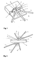
- FIG. 1 An arrangement with a sample 1 is schematically for the slope etching method in FIG FIG. 1 shown.
- the present method is particularly well suited for the more complex and delicate slope etching process.
- the sample 1 is cut out of the material to be examined.
- a planar mask 2 is brought to a selected sample surface 3, the surface of which is advantageously arranged perpendicular to the sample surface.
- the mask is arranged slightly spaced from the sample surface 3, which adjoins at a distance in the range of 10 .mu.m to 100 .mu.m and thereby form the two surfaces in this area an adjacent line.
- the impingement zone 4 of the at least three, preferably three, ion beams J 1 , J 2 , with their beam diameter q, is placed.
- the ion beams J lie in a plane 10 and the plane passes through this line.
- This plane 10 with the ion beams is advantageously positioned perpendicular to the sample surface 3 and may be parallel to the surface of the mask 2.
- the plane 10 may also be slightly tilted relative to the surface of the mask 2 by an angle in the range of 0 ° to 10 °, preferably from 0 ° to 5 °.
- the material is preferably removed from the sample 1 in the direction of the ion beams J, whereby a kind of trench is formed with the now deeper impingement zone 4 '.
- the impact zone 4, 4 'thus shifts, depending on the progress of the etching process.
- Laterally to the plane 10 and thus laterally to the ion beams within the sample 1 is also easily etched by grazing or scattering ions and there is a so-called slope 5 at the desired location to be considered which forms the observation surface 20 shown.
- the observation direction 12 for the SEM is aligned, with advantage, perpendicular to the lateral sample surface and in particular to the observation surface 20.
- the ion beams J are all aligned in a plane 10. These can enclose different angles ⁇ , ⁇ ', ⁇ "and thus form a kind of circle segment
- the clamped circle segment advantageously includes an angle ⁇ which lies in the range of 10 ° to 180 °, preferably in the range of 30 ° to 140 °
- there are also other ion beams within the circle segment which is closed by the two ion beams which enclose the largest angle and bound the circle segment
- the ion beams can be symmetrical or asymmetrical be aligned to a vertical N to the sample surface, as shown schematically in the FIGS. 5a to 5c is shown.
- the circular segment thus formed with the central axis Z can also be tilted in relation to this vertical N by an angle ⁇ for further adjustment of desired etching conditions.
- the angle ⁇ is advantageously in the range of ⁇ 20 °, preferably in the range of ⁇ 10 °.
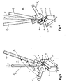
- FIGS. 3 and 4 there is shown an arrangement according to the wire shading method, which is also a preferred preparation for the present method.
- the figures show two different views in which the sample 1 is shown slightly rotated for clarity.
- this sample 1 often has a structured surface 3, which may additionally contain coatings or layer systems (not shown).
- a wire or a fiber 7 with a small predetermined diameter is fixed on the sample surface 3, for example with an adhesive. It is customary to choose a sample width d of about 100 ⁇ m or less to 10 ⁇ m the fiber to be applied is smaller in diameter than the sample width d and forms a mask.
- at least three, preferably three, ion beams J, preferably perpendicular to the sample surface 3, are then directed onto the fiber 7 where the impact zone 4 is then located. In this case, the vertical N lies within the plane 10.
- the plane 10 is placed parallel to the direction of the wire or even passes through the wire axis.
- the sample 1 is etched so strongly by the ion beams J that there is a clear wedge-shaped formation transverse to its length l.
- the etched flanks 6 on both sides of the sample 1 now enclose an elongated comb which tapers and is electron-permeable in this region for a TEM observation which takes place from the side of the sample, preferably in the vertical direction of observation 12, with an arrow transverse to the sample longitudinal direction is shown.
- the fiber 2 is also strongly etched in this state.
- the ion beams form a kind of circle segment within the plane 10 and the ion beams can impinge on the sample surface 3 at different angles or be tilted as a whole.
- the clamped-on circular segment advantageously includes an angle .alpha. Which is in the range of 10.degree. To 180.degree., Preferably in the range of 30.degree. To 140.degree., And all ion beams lie in the plane 10 of this circular segment spanned by the latter. Depending on the number is, preferably in the range of 30 ° to 140 ° and all the ion beams are in the plane spanned by this plane 10 of this circle segment.
- there are also other ion beams within the circle segment which is terminated by the two ion beams, which enclose the aforementioned largest angle and bound the circle segment.
- the ion beams may be oriented symmetrically or asymmetrically to a perpendicular N to the sample surface, as shown schematically in FIGS FIGS. 5a to 5c is shown.
- the circular segment thus formed with the central axis Z can also be tilted in relation to this vertical N by an angle ⁇ for further adjustment of desired etching conditions.
- the angle ⁇ is advantageously chosen to be in the range of ⁇ 20 °, preferably in the range of ⁇ 10 °.
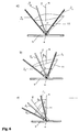
- FIGS. 5a to 5b are various possible positions and directions of incidence of ion beams J, which are guided in a common plane (10) lying opposite to the sample surface, shown schematically.
- FIG. 5a is located by the two ion beams J 1 , J 2 at the angle ⁇ limited circle segment with its central axis of symmetry Z on the vertical N to the sample surface 3 on which the impingement zone 4 is for all ion beams J and in which these are brought together in a kind of intersection.
- the two ion beams J 1 , J 2 are guided with respect to the central axis Z and the vertical N by the angle ⁇ / 2 in the direction of the impact zone.
- the circular segment with the central axis Z can be tilted with respect to the vertical N by an angle ⁇ , ie have a corresponding asymmetry, as shown in the FIG. 5b is shown.
- a tilt in which all ion beams come to lie on one side of the vertical N is in FIG. 5c
- the three ion beams J1-J3 are guided at corresponding angles ⁇ lying on a conical surface 11 whose tip is in the impact zone 4 lies, as in the FIGS. 6a to 6c is shown.
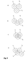
- FIGS. 7a to 7d Different combinations of the at least three ion beams J in the area of the impact zone 4 are in the FIGS. 7a to 7d shown in supervision.
- the ion beams with their cross-section q are all in the same plane 10 and touch each other in the impact zone at least as shown in FIG Figure 7a , These are all in a line within the plane 10 which intersects the impact zone 4. They can overlap individually according to FIG. 7b or all overlap according to FIG. 7c or touch and overlap according to FIG. 7d ,
- FIGS. 8a to 8d The merging of at least three ion beams J within an impingement zone 4 for ion beams J which lie on at least one conical surface and / or also in between is in the FIGS. 8a to 8d shown.
- FIG. 8a shows three contacting ion beams J 1 to J 3 in the impingement zone 4.
- Three partially overlapping ion beams are in FIG. 8b shown.
- Three overlapping ion beams are in FIG. 8c shown and four ion beams overlapping and touching in the FIG. 8d ,
Description
Die Erfindung bezieht sich auf Verfahren zur Herstellung einer Probe für die Elektronenmikroskopie, die aus einem Festkörpermaterial geschnitten wird gemäss Oberbegriff nach Anspruch 1.The invention relates to a method for producing a sample for electron microscopy, which is cut from a solid material according to the preamble of
Proben für die Elektronenmikroskopie können auf verschiedene Art und Weise präpariert werden. Um Proben mit einem Elektronenmikroskop betrachten zu können, müssen diese entsprechend definiert bearbeitet werden durch Freilegen der zu betrachtenden Beobachtungsoberfläche mittels eines Ätzverfahrens. Bei rasterelektronenmikroskopischer (REM) Betrachtung wird die gewünschte Oberfläche betrachtet. Bei Betrachtung der Probe mit einem Transmissionselektronenmikroskop (TEM) wird die Probe durch das Ätzen derart gedünnt, dass diese im TEM von den Elektronen durchstrahlt werden können und die Probe in Transmission betrachtet werden kann. Hierbei ist die Qualität der Bildauflösung ganz wesentlich von der Qualität der Probe abhängig. Dafür sollte die Probe auf einen entsprechend gewünschten Oberflächenbereich für die REM - Methode oder auf eine gewünschte definierte Dicke für die TEM - Methode gleichförmig eingestellt werden durch einen entsprechend geeigneten Ätzvorgang. Hierbei ist es wichtig, dass bei diesem Ätzvorgang die Probenstruktur nicht durch den Vorgang selbst verändert wird. Zur Herstellung einer solchen Probe wird zuerst ein Stück des zu untersuchenden Materiales aus dem Probenkörper mechanisch herausgesägt und anschliessend durch Ätzen behandelt, um die Probe anschliessend mit einem REM oder TEM untersuchen zu können. Die nasschemische Ätzmethode ist diesbezüglich nicht zielführend. Aus diesem Grunde werden heute für die hochqualitativen elektronenmikroskopischen Betrachtungen mit REM oder TEM, die Proben mit einem Ionenstrahl durch Ionenätzen, wie Sputterätzen, im Vakuum bearbeitet. Als Ionenstrahl wird beispielsweise ein Argon-Ionenstrahl mit einem Durchmesser von ca. 1 mm verwendet.Samples for electron microscopy can be prepared in a variety of ways. In order to be able to view samples with an electron microscope, they must be correspondingly processed by exposing the observation surface to be observed by means of an etching process. By scanning electron microscopic (SEM) observation, the desired surface is observed. When viewing the sample with a transmission electron microscope (TEM), the sample is thinned by the etching such that they can be irradiated by the electrons in the TEM and the sample can be viewed in transmission. The quality of the image resolution is very much dependent on the quality of the sample. For this, the sample should be uniformly adjusted to a corresponding desired surface area for the SEM method or to a desired defined thickness for the TEM method by a suitably suitable etching process. In this case, it is important that the sample structure is not changed by the process itself during this etching process. To produce such a sample, first a piece of the material to be examined is mechanically sawn out of the sample body and then treated by etching in order to subsequently examine the sample with a SEM or TEM. The wet-chemical etching method is not effective in this respect. For this reason, today, for high-quality electron microscopic observation with SEM or TEM, the samples are processed with an ion beam by ion etching such as sputter etching in a vacuum. As the ion beam, for example, an argon ion beam having a diameter of about 1 mm is used.
Proben für die Elektronenmikroskopie können mittlerweile auf verschiedene Art präpariert werden. Es sind heute insbesondere drei Verfahren bekannt für die Bearbeitung von Proben mit Ionenstrahlätzen.Samples for electron microscopy can now be prepared in various ways. In particular, three methods are known today for processing samples with ion beam etching.
Das Ionenstrahl - Böschungsätzen ist ein Verfahren, das seit längerer Zeit zur Herstellung von Querschnittsproben für die Rasterelektronenmikroskopie (REM) genutzt wird. Bei diesem Verfahren wird ein Teil der Probenoberfläche mit einer Maske abgedeckt. Der nicht abgedeckte Teil der Oberfläche wird ionengeätzt, bis eine Art Böschung entsteht. An dieser Böschung kann die Querschnittsstruktur der Probe untersucht werden. Die erzielten Schnittiefen liegen im Bereich von wenigen 2.0 µm bis maximal 50 µm. Die Präparationszeiten variieren je nach Material und Ätztiefe zwischen einigen Minuten und mehreren Stunden. Um eine gleichmässig abgetragene Schnittfläche zu erhalten, muss die Probe während des Ätzens oszillieren. Das gilt besonders für strukturierte Materialien mit stark unterschiedlichen Sputterraten, wie sie in der Halbleiterindustrie vorkommen. Die momentan bekannten verwendeten Verfahren und Techniken zur Herstellung eines Böschungsschnittes verwenden nur eine einzelne Ionenquelle bzw. einen einzelnen Ionenstrahl.Ion beam slope etching is a technique that has long been used to produce SEM cross-section samples. In this method, a part of the sample surface is covered with a mask. The uncovered part of the surface is ion etched until a kind of embankment is created. At this slope, the cross-sectional structure of the sample can be examined. The achieved cutting depths are in the range of a few 2.0 μm to a maximum of 50 μm . The preparation times vary from a few minutes to several hours, depending on the material and the depth of the etching. In order to obtain a uniform cut surface, the sample must oscillate during the etching. This is especially true for structured materials with very different sputtering rates, as they occur in the semiconductor industry. The currently known methods and techniques for making a slope cut use only a single ion source or ion beam.
Die zunehmenden Anforderungen besonders aus dem Bereich der Mikroelektronik gehen in Richtung grosser Schnittiefen von bis zu einem mm oder mehr bei gleichzeitig kurzer Präparationszeit und exzellenter Präparationsqualität, welche mit diesem bekannten Verfahren nicht erreicht werden kann.The increasing demands, especially in the field of microelectronics, go in the direction of large cutting depths of up to one mm or more with simultaneous short preparation time and excellent preparation quality, which can not be achieved with this known method.
Ein weiteres bekanntes Präparationsverfahren ist das sogenannte Drahtabschattungsverfahren. Das Verfahren der Drahtabschattung wird zur Herstellung von TEM-Proben mit extrem grossen elektronentransparenten Bereichen (mehrere mm lang) genutzt (Patent
Diese Anforderungen sind mit der momentanen Ätztechnik sowohl für das Böschungsschnittverfahren als auch für die Drahtabschattung nicht zu erfüllen.These requirements can not be met with the current etching technique for both the slope cutting method and the wire shading.
Ein weiteres bekanntes und verbreitetes Präparationsverfahren ist die TEM-Standard Präparation. Bei der Ionenstrahlpräparation von TEM-Standard-Proben wird eine mechanisch vorpräparierte Probe von ca. 3mm Durchmesser und ca. 20 bis 50 µm Dicke entweder mit zwei Ionenquellen von einer Probenseite her, oder jeweils je einer Ionenquelle auf jeder Probenseite, als auf der vorderen und hinteren Seite gleichzeitig geätzt. Während dem Ätzvorgang rotiert oder oszilliert die Probe, um Ätzstrukturen zu vermeiden. Alternativ kann auch der Ionenstrahl relativ zur Probe bewegt werden oder beides. Auch bei diesem Verfahren sind die Anforderungen in Richtung hoher Ätztiefe bei gleichzeitig geringer Ätzzeit und exzellenter Probenqualität nicht, oder nur mit grossem Aufwand, zu realisieren.Another well-known and widespread preparation method is the TEM standard preparation. For ion beam preparation of standard TEM specimens, a mechanically prepared specimen about 3 mm in diameter and about 20 to 50 μm in thickness is made either with two ion sources from one sample side, or one ion source on each side of the specimen, than on the front and back etched on the rear side at the same time. During the etching process, the sample rotates or oscillates to avoid etch structures. Alternatively, the ion beam may be moved relative to the sample, or both. Also in this method, the requirements in the direction of high etching depth with low etching time and excellent sample quality are not, or only with great effort to realize.
Die Patentschrift
In der Patentschrift
Die Patentschrift
Der Erfindung liegt die Aufgabe zugrunde, die Nachteile des Standes der Technik zu beseitigen. Es soll insbesondere ein Ätzverfahren realisiert werden, welches hohe Schnittiefen bei kurzer Präparationszeit ermöglicht, mit welchem bei hoher Zuverlässigkeit und guter erreichbarer Probenqualität eine hohe Wirtschaftlichkeit erreicht werden kann.The invention has for its object to eliminate the disadvantages of the prior art. In particular, an etching method is to be realized which enables high depths of cut with a short preparation time, with which a high degree of cost-effectiveness can be achieved with high reliability and good achievable sample quality.
Die Aufgabe wird erfindungsgemäss durch Vorgehen nach dem Verfahren nach Anspruch 1 gelöst. Die abhängigen Ansprüche definieren weitere vorteilhafte Verfahrensschritte.The object is achieved according to the invention by proceeding according to the method of
Erfindungsgemäss werden elektronenmikroskopische Proben mit mindestens drei örtlich fest angeordneten Ionenstrahlen geätzt, welche unter einem Winkel auf die Probenoberfläche gerichtet sind und sich dort treffen. Die Proben werden hierbei ebenfalls nicht bewegt, so dass keine Relativbewegung zwischen den Ionenstrahlen und der Probe vorhanden ist, womit die ganze Anordnung stationär angeordnet betrieben wird.According to the invention, electron microscopic samples are etched with at least three fixedly arranged ion beams which are directed at an angle onto the sample surface and meet there. The samples are also not moved in this case, so that there is no relative movement between the ion beams and the sample, with which the entire arrangement is operated stationarily arranged.
einem Festkörpermaterial geschnitten, beispielsweise mechanisch. Eine zusätzliche chemische und / oder mechanische Behandlung ist möglich: Danach wird eine an der Probe ausgebildete Probenoberfläche mit einem Ionenstrahl unter einem vorgegebenen Einfallswinkel derart behandelt, dass Material von der Probenoberfläche durch Ionenätzen abgetragen wird bis an der Probe, im Bereich der Auftreffzone des Ionenstrahles, die gewünschte Beobachtungsoberfläche freigelegt ist, welche anschliessend die Betrachtung im gewünschten Bereich der Probe mit einem Elektronenmikroskop ermöglicht, wobei mindestens drei feststehende Ionenstrahlen unter einem vorgegebenen Winkel zueinander ausgerichtet auf die Probenoberfläche geführt werden, derart dass sich die Ionenstrahlen an der Probenoberfläche zumindest berühren oder schneiden und dort eine Auftreffzone bilden, und dass sowohl die Probe, wie auch die Ionenstrahlen nicht bewegt und somit stationär betrieben werden.a solid state material cut, for example mechanically. An additional chemical and / or mechanical treatment is possible: Thereafter, a sample surface formed on the sample is treated with an ion beam at a predetermined angle of incidence so that material is removed from the sample surface by ion etching up to the sample, in the region of the impact zone of the ion beam, the desired observation surface is exposed, which then allows viewing in the desired region of the sample with an electron microscope, wherein at least three fixed ion beams are guided at a predetermined angle aligned with each other on the sample surface, so that the ion beams at least touch or cut on the sample surface and There form an impact zone, and that both the sample, as well as the ion beams are not moved and thus operated stationary.
Das vorliegende Ätzverfahren ermöglicht die ruhende Probe während des Ätzvorganges in hoher Auflösung mit einem Beobachtungsmittel zu betrachten und somit den Vorgang zu kontrollieren, vorzugsweise mit einem Lichtmikroskop oder einem Rasterelektronenmikroskop. Diese Beobachtung sollte mindestens zeitweise erfolgen über den Verlauf des gesamten Ätzvorganges.The present etching method makes it possible to observe the quiescent sample during the etching process in high resolution with an observation means and thus to control the process, preferably with a light microscope or a scanning electron microscope. This observation should be made at least temporarily over the course of the entire etching process.
Die Probe wird mit Vorteil vor dem Ionenätzen gegenüber dem Beobachtungsmittel ausgerichtet und während dem Ätzvorgang nicht mehr bewegt.The sample is advantageously aligned with the observation means prior to ion etching and is not moved during the etching process.
Die Probe kann während dem Ätzvorgang zusätzlich gekühlt werden , insbesondere, um noch höhere Strahlleistungen zulassen zu können, welche in der Folge noch höhere Ätzgeschwindigkeiten ermöglichen, auch bei sehr empfindlichen Proben.The sample can additionally be cooled during the etching process, in particular in order to be able to allow even higher beam powers, which in the sequence allow even higher etching speeds, even with very sensitive samples.
Damit ist es möglich hohe Schnittiefen bei kurzer Präparationszeit zu erreichen. Es wird eine hohe Oberflächenqualität erzielt und Ätzselektivitäten werden gering gehalten oder vermieden. Die Bedingungen hierzu können optimal gewählt und an der Anordnung eingestellt werden, beispielsweise durch die Wahl des Winkels zwischen den Ionenstrahlen, des Auftreffwinkels der Ionenstrahlen auf der Probenoberfläche, gleicher oder verschiedener Energie der Strahlen, Strahldurchmesser, Strahlstromdichte und Lage der Strahlen im Auftreffbereich der Probe. Die Werte können einzeln und / oder in Kombination vorgegeben, eingestellt oder variiert werden. Auch können die Werte nach vorgegebenem Programm, beispielsweise mit einer automatisierten Steuerung, abhängig vom Fortschritt des Ätzvorganges variiert oder nachgeführt werden. Mit Vorteil werden für eine TEM - Probe mindestens drei feststehende Ionenstrahlen verwendet, diese müssen nicht in einer Ebene liegen. Für Proben nach dem Böschungsätzverfahren oder dem Drahtabschattungsverfahren werden auch bereits mit drei feststehenden Ionenstrahlen günstige Ergebnisse erzielt. Drei oder mehr Ionenstrahlen bringen noch bessere Ergebnisse und es ist dann vorteilhaft, wenn diese drei oder mehr Ionenstrahlen in einer einzelnen Ebene liegend an die Probe geführt werden.This makes it possible to achieve high cutting depths with a short preparation time. It achieves a high surface quality and Ätzselektivitäten be kept low or avoided. The conditions for this can be optimally selected and set at the arrangement, for example by the choice of the angle between the ion beams, the angle of incidence of the ion beams on the sample surface, same or different energy of the beams, beam diameter, beam current density and position of the beams in the impact area of the sample. The values can be predetermined, adjusted or varied individually and / or in combination. Also, the values may be varied or tracked according to a predetermined program, for example with an automated control, depending on the progress of the etching process. Advantageously, at least three fixed ion beams are used for a TEM sample, these need not lie in one plane. For samples according to the embankment etching method or the wire shading method, favorable results are achieved even with three fixed ion beams. Three or more ion beams produce even better results, and it is advantageous if these three or more ion beams are guided in a single plane to the sample.
Für die Präparation von beispielsweise Solder Balls ist das Böschungsätzen sehr geeignet. Bei derartigen Strukturen führt die Anwendung einer Oszillationsbewegung, entsprechend den bekannten Verfahren, durch die unterschiedlichen auftretenden Beschusswinkel bei der Oszillation zu einem sehr unerwünschten "Tunneleffekt". Das kann durch Vorgehen gemäss der Erfindung, durch den Einsatz von mehreren feststehenden Ionenstrahlen und allenfalls zusätzlich durch den Einsatz von unterschiedlichen Energien der einzelnen Ionenstrahlen nun gut unterdrückt werden.For the preparation of, for example, Solder Balls, embankment etching is very suitable. In such structures, the application of an oscillatory movement, in accordance with the known methods, leads to a very undesirable "tunneling effect" due to the different firing angles occurring during the oscillation. This can now be well suppressed by the procedure according to the invention, by the use of several fixed ion beams and possibly additionally by the use of different energies of the individual ion beams.
Die Ionenstrahlen können für jeden Strahl mit einer eigenen Ionenquelle erzeugt werden oder es können auch mit Vorteil mindestens zwei Ionenstrahlen mit einer einzelnen Ionenquelle erzeugt werden, indem diese aus einer gemeinsamen Quellenanordnung, wie einem Plasma, durch Extraktion erzeugt werden.The ion beams may be generated for each beam with its own ion source, or it may be advantageous to generate at least two ion beams with a single ion source by extraction from a common source array, such as a plasma.
In einem bevorzugten Ausführungsbeispiel werden drei Ionenquellen, in einem Gehäuse integriert, in einem Winkel von jeweils 60° zueinander angeordnet. Die Ionenstrahlen bilden einen Schnittpunkt, der auf einen ausgewählten Punkt bzw. einer Auftreffzone auf der Probenoberfläche gerichtet werden kann. Die Strahlen bilden einen Kreissektor von 60° bis 120°. Die Strahlen müssen hierbei aus verschiedenen Richtungen auf die Probenoberfläche treffen, so dass ein Winkel von 0° bis 180°, vorzugsweise 20° bis 160° bezüglich der Probenoberfläche entsteht, abhängig vom Anwendungsfall, (Ätztiefe oder Ätzbreite) und dass ein Schnittpunkt der Einzelstrahlen auf einer wählbaren Auftreffzone auf der Probe entsteht. Der Kreissektor kann durch zwei oder mehr Strahlen gebildet werden. Dies kann durch mehrere Ionenstrahlen, extrahiert aus einer oder mehreren Ionenquellen, realisiert werden. Der Winkel des Kreissektors beeinflusst die Schnittgeschwindigkeit bzw. die Oberflächenqualität.In a preferred embodiment, three ion sources, integrated in a housing, are arranged at an angle of 60 ° to each other. The ion beams form an intersection that can be directed to a selected point or landing area on the sample surface. The rays form a circular sector of 60 ° to 120 °. The beams have to be different Make directions on the sample surface, so that an angle of 0 ° to 180 °, preferably 20 ° to 160 ° with respect to the sample surface is formed, depending on the application, (etch depth or Ätzbreite) and that an intersection of the individual beams on a selectable impact zone on the sample arises. The circular sector can be formed by two or more beams. This can be realized by multiple ion beams extracted from one or more ion sources. The angle of the circular sector influences the cutting speed or surface quality.
Bei einem weiteren bevorzugten Ausführungsbeispiel für das Böschungsätzverfahren werden drei jeweils um 60° versetzte Ionenquellen, die einen Kreissektor bilden (60° bis 120°) verwendet. Mit der Einstellung der Winkelgrösse können unterschiedliche Resultate erreicht werden und dadurch je nach Wunsch eingestellt werden. Ein kleinerer Winkel, beispielsweise von 60° bis 120°, führt zu einer höheren Schnittgeschwindigkeit, aber andererseits besonders bei Proben mit hoher Ätzselektivität, zu stärker ausgebildeten Vorzugsrichtungen.In a further preferred embodiment for the slope etching method, three ion sources each offset by 60 ° and forming a circular sector (60 ° to 120 °) are used. With the adjustment of the angle size, different results can be achieved and thus adjusted as desired. A smaller angle, for example, from 60 ° to 120 °, leads to a higher cutting speed, but on the other hand, especially for samples with high Ätzselektivität, to more pronounced preferred directions.
Die Ionenenergie der Strahlen liegt im Bereich von 200 eV bis 12 keV, vorzugsweise im Bereich von 500 eV bis 8 keV. Die Ionenenergie der Einzelquellen kann variiert werden, um bestimmte Ätzprofile zu erreichen.The ion energy of the beams is in the range of 200 eV to 12 keV, preferably in the range of 500 eV to 8 keV. The ion energy of the single sources can be varied to achieve certain etch profiles.
Durch das Berühren und / oder Überlappen der einzelnen Ionenstrahlen aus verschiedenen Richtungen in einem Schnittbereich an der Auftrefffläche der Probenoberfläche wird der oben genannte Beschusssektor gebildet, der eine Rotation der Probe zur Vermeidung von Vorzugsrichtungen unnötig macht. Die Position des Schnittbereichs kann justiert, oder gar geregelt, werden, auch während dem Ätzprozess. Dadurch ist der Einfluss des Profils des Einzelstrahles geringer und das Verfahren ist weniger kritisch in den Einstellungen, womit die Zuverlässigkeit erhöht ist.By touching and / or overlapping the individual ion beams from different directions in a cutting area on the surface of the sample surface, the above-mentioned bombardment sector is formed, which makes a rotation of the sample unnecessary to avoid preferential directions. The position of the cutting area can be adjusted, or even controlled, even during the etching process. As a result, the influence of the profile of the single beam is lower and the method is less critical in the settings, which increases the reliability.
Ionenenergie und Stromdichte sind beispielsweise auch in Abhängigkeit von der thermischen Empfindlichkeit der Probe wählbar. Das vorgestellte Verfahren ermöglicht somit durch die gezielte Einstellbarkeit von wichtigen Parametern einen hohen Grad an Flexibilität bei der Prozessführung, womit eine Anpassung an die verschiedensten Proben leicht möglich ist und dies bei hoher Prozessproduktivität.Ion energy and current density can also be selected, for example, depending on the thermal sensitivity of the sample. The presented method thus enables a targeted adjustability of important parameters high degree of process control flexibility, making it easy to adapt to a wide range of samples with high process productivity.
Die Erfindung wird nun nachfolgend beispielsweise und anhand von schematischen Zeichnungen näher erläutert. Es zeigen:
- Fig. 1
- Eine Probe in dreidimensionaler Darstellung für das Böschungsätzen mit drei Ionenstrahlen in einer Ebene liegend gemäss der Erfindung;
- Fig. 2
- Eine Probe in dreidimensionaler Darstellung für eine TEM Standardprobe mit beidseitigem Ätzen mit jeweils drei Ionenstrahlen gemäss der Erfindung;
- Fig. 3
- Eine Probe in dreidimensionaler Darstellung für das Drahtabschattungsverfahren mit drei Ionenstrahlen in einer Ebene liegend gemäss der Erfindung, wobei ein Ionenstrahl senkrecht,zur Probenoberfläche auftrifft;
- Fig. 4
- Eine Probe in dreidimensionaler Darstellung entsprechend der
Figur 3 in gedrehter Ansicht und nicht senkrecht auftreffendem Ionenstrahl; - Fig. 5a-c
- Im Querschnitt Ionenstrahlen in einer Ebene liegend unter verschiedenen möglichen Winkeln zueinander und unterschiedlichen möglichen Auftreffwinkeln auf die Probenoberfläche;
- Fig. 6a-c
- Im Querschnitt Ionenstrahlen auf einer Kegelfläche liegend unter verschiedenen möglichen Winkeln zueinander und unterschiedlichen möglichen Auftreffwinkeln auf die Probenoberfläche;
- Fig. 7a-d
- In der Aufsicht zur Probenoberfläche verschiedene mögliche Formen der Auftreffzone für mehrere Ionenstrahlen bei Berührung und / oder Überlappung in einer Linie liegend bei Ionenstrahlen, die in einer Ebene liegen; Probenoberfläche
- Fig. 8a-d
- In der Aufsicht zur verschiedene mögliche Formen der Auftreffzone für mehrere Ionenstrahlen bei Berührung und / oder Überlappung bei Ionenstrahlen, die nicht in einer Ebene liegen, beispielsweise auf einer Kegelmantelfläche.
- Fig. 1
- A sample in three-dimensional representation for the slope etching with three ion beams lying in a plane according to the invention;
- Fig. 2
- A sample in three-dimensional representation for a TEM standard sample with double-sided etching, each with three ion beams according to the invention;
- Fig. 3
- A sample in three-dimensional representation for the wire shading method with three ion beams in a plane according to the invention, wherein an ion beam impinges perpendicular to the sample surface;
- Fig. 4
- A sample in three-dimensional representation according to the
FIG. 3 in rotated view and not perpendicularly incident ion beam; - Fig. 5a-c
- In cross-section ion beams lying in a plane at different possible angles to each other and different possible angles of incidence on the sample surface;
- Fig. 6a-c
- In cross section, ion beams lying on a conical surface at different possible angles to each other and different possible angles of incidence on the sample surface;
- Fig. 7a-d
- In the supervision of the sample surface various possible shapes of the impact zone for multiple ion beams in contact and / or Overlap in line with ion beams lying in a plane; sample surface
- Fig. 8a-d
- In the plan view of various possible shapes of the impact zone for multiple ion beams in contact and / or overlap with ion beams, which are not in a plane, for example on a conical surface.
Ein flacher Probenkörper 1 wird beispielsweise mit einem Diamantwerkzeug aus dem zu untersuchenden Material geschnitten und beidseitig mechanisch poliert. Die Probe 1 weist dann zwei Seiten auf mit den zwei Oberflächen 3a und 3b und der Dicke d, wie dies in
Eine Anordnung mit einer Probe 1 ist für das Böschungsätzverfahren schematisch in
Durch den nun folgenden Ätzvorgang, beginnend an der Auftreffzone 4 der ursprünglichen Probenoberfläche 3 wird das Material bevorzugt in der Richtung der Ionenstrahlen J von der Probe 1 abgetragen, wodurch eine Art Graben entsteht mit der nun tiefer liegenden Auftreffzone 4'. Die Auftreffzone 4, 4' verschiebt sich somit , abhängig zum Fortschritt des Ätzvorganges. Seitlich zur Ebene 10 und somit seitlich zu den Ionenstrahlen innerhalb der Probe 1 wird ebenfalls durch streifende bzw. streuende Ionen leicht geätzt und es entsteht eine sogenannte Böschung 5 am gewünschten zu betrachtenden Ort welche die erzeigte Beobachtungsfläche 20 bildet. Bei einer derartigen Probe wird die Beobachtungsrichtung 12 für das REM, mit Vorteil, in senkrecht zur seitlichen Probenoberfläche und insbesondere zur Beobachtungsfläche 20 ausgerichtet.By the following etching process, starting at the
Bei dieser bevorzugten Anwendung werden die Ionenstrahlen J alle in einer Ebene 10 ausgerichtet. Diese können verschiedene Winkel α, α', α" einschliessen und bilden somit eine Art Kreissegment. Das aufgespannte Kreissegment schliesst hierbei mit Vorteil einen Winkel α ein der im Bereich von 10° bis 180° liegt, vorzugsweise im Bereich von 30° bis 140° und alle Ionenstrahlen liegen in der durch diese aufgespannten Ebene 10 dieses Kreissegmentes. Je nach Anzahl der Ionenstrahlen liegen auch weitere Ionenstrahlen innerhalb des Kreissegmentes welches abgeschlossen wird durch die zwei Ionenstrahlen, die den grössten Winkel einschliessen und das Kreissegment begrenzen. Die Ionenstrahlen können symmetrisch oder asymmetrisch zu einer Senkrechten N zur Probenoberfläche ausgerichtet werden, wie dies schematisch in den
In den
mit der Länge l und der Breite d. Wenn es sich um eine Probe handelt, die aus einem Mikroelektronikwafer geschnitten ist, weist diese Probe 1 oft eine strukturierte Oberfläche 3 auf, welche zusätzlich Beschichtungen oder Schichtsysteme enthalten können (nicht gezeigt). Ein Draht oder eine Faser 7 mit kleinem vorgegebenen Durchmesser ist auf der Probenoberfläche 3, beispielsweise mit einem Klebstoff, fixiert. Es ist üblich eine Probenbreite d von etwa 100 µm zu wählen oder geringer bis 10 µm die zu applizierende Faser ist im Durchmesser kleiner als die Probenbreite d und bildet eine Maske. Gemäss vorliegender Erfindung werden nun mindestens drei, vorzugsweise drei, Ionenstrahlen J, vorzugsweise senkrecht zur Probenoberfläche 3, auf die Faser 7 gerichtet wo dann die Auftreffzone 4 liegt. In diesem Fall liegt die Senkrechte N innerhalb der Ebene 10. Die Ebene 10 wird parallel zur Richtung des Drahtes gelegt oder führt gar durch die Drahtachse.with the length l and the width d. In the case of a sample cut from a microelectronic wafer, this
Nach einer gewissen Ätzzeit bilden sich durch den Materialabtrag der Probe 1 beidseitig zur Probe 1 Flanken 6 aus, welche am Ende des Ätzvorganges die Beobachtungsoberfläche 20 für das TEM bilden. Es ist auch erkenntlich, dass eine kammartige Zuspitzung der Probe ausgebildet wird, wie dies aus den
Auch hier wird durch die Ionenstrahlen, wie zuvor beim Böschungsätzen beschrieben, eine Art Kreissegment gebildet innerhalb der Eben 10 und die Ionenstrahlen können unter verschiedenen Winkeln auf die Probenoberfläche 3 gerichtet auftreffen oder als ganzes verkippt angeordnet sein. Das aufgespannte Kreissegment schliesst hierbei mit Vorteil einen Winkel α ein der im Bereich von 10° bis 180° liegt, vorzugsweise im Bereich von 30° bis 140° und alle Ionenstrahlen liegen in der durch diese aufgespannten Ebene 10 dieses Kreissegmentes. Je nach Anzahl liegt, vorzugsweise im Bereich von 30° bis 140° und alle Ionenstrahlen liegen in der durch diese aufgespannten Ebene 10 dieses Kreissegmentes. Je nach Anzahl der Ionenstrahlen liegen auch weitere Ionenstrahlen innerhalb des Kreissegmentes welches abgeschlossen wird durch die zwei Ionenstrahlen, die den vorerwähnten grössten Winkel einschliessen und das Kreissegment begrenzen.Here again, the ion beams, as described above for embankment etching, form a kind of circle segment within the
Die Ionenstrahlen können symmetrisch oder asymmetrisch zu einer Senkrechten N zur Probenoberfläche ausgerichtet werden, wie dies schematisch in den
In den
Das Kreissegment mit der Zentralachse Z kann gegenüber der Senkrechten N um einen Winkel β verkippt angeordnet sein, also eine entsprechende Asymmetrie aufweisen, wie dies in der
Verschiedene Zusammenführungen der mindestens drei Ionenstrahlen J im Bereich der Auftreffzone 4 sind in den
Die Zusammenführung von mindestens drei Ionenstrahlen J innerhalb einer Auftreffzone 4 für Ionenstrahlen J, die mindestens auf einer Kegelmantelfläche und /oder auch dazwischen liegen ist in den
Claims (15)
- Method for production of a sample (1) for electron microscopy which is cut from a solid body material, with a sample surface (3) formed thereon which is treated with an ion beam (J) at a predefined angle of incidence, such that material is removed from the sample surface (3) by etching until on the sample (1), in the region of the impact zone (4) of the ion beam (J), the desired observation surface (20) is exposed which allows viewing (12) with an electron microscope in the desired region of the sample (1), characterised in that at least three fixed ion beams (J1, J2, J3) are guided at a predefined angle (α) to each other onto the sample surface (3) such that the ion beams (J1, J2, J3) at least touch or intersect at the sample surface (3) and there form an impact zone (4), and that both the sample (1) and the ion beams (J1, J2, J3) are not moved and are therefore operated stationary.
- Method according to claim 1, characterised in that the sample (1) is treated with the ion beams (J1, J2, J3) in the slope etching process.
- Method according to claim 1, characterised in that the sample (1) is treated with the ion beams (J1, J2, J3) in the wire shadowing process.
- Method according to claim one, characterised in that a standard TEM sample (1) is treated with the ion beams (J1, J2) in that in each case at least three ion beams (J1, J2) are directed onto at least one of the sample sides (3a, 3b) to remove the sample surface (3a, 3b).
- Method according to any of the preceding claims, characterised in that several stationary ion beams (J1, J2), preferably three, are guided a different angles (α, α', α") onto the sample surface (3) and there all at least touch or preferably at least partially overlap in the impact zone (4).
- Method according to any of the preceding claims, characterised in that the mutual position of the ion beams (J1, J2) in the impact zone (4) and hence the degree of overlap can be adjusted for at least one ion beam, preferably during the etching process.
- Method according to any of the preceding claims, characterised in that at least two of the ion beams (J1, J2) are generated jointly with a single ion source.
- Method according to any of the preceding claims, characterised in that at least two of the ion beams (J1, J2) are generated separately each with their own ion source.
- Method according to any of the preceding claims, characterised in that during the etching process, the resting sample (1) is observed for at least part of the time in high resolution with an observation means, preferably a light-optical microscope or a scanning electron microscope.
- Method according to claim 2, characterised in that in ion beam slope etching, a mask (2) with a planar surface is used which connects to the sample surface (3) at a distance in the range from 10 µm to 100 µm, and thus the two surfaces in this region form a bordering line, in the region of which lies the impact zone (4) of the ion beams (J1, J2, J3), and that the ion beams span a plane (10) in which this line lies, wherein this plane (10) is arranged slightly tilted in relation to the surface of the mask (2) by an angle in the range from 0 to 10°, preferably from 0° to 5°, and that the surface of the mask (2) is positioned preferably vertical to the sample surface (2).
- Method according to claim 2 or 10, characterised in that the ion beams (J1, J2, J3) span a circle segment with an angle (α) and this lies in the range from 10° to 180°, preferably in the range from 30° to 140°, and that all ion beams (J1, J2, J3) lie in the plane of this circle segment.
- Method according to claim 3, characterised in that in the wire shadowing process, the ion beams (J1, J2, J3) are guided in a plane (10) which lies parallel to the wire (7), wherein the normal (N) to the sample surface (3) also lies in this plane (10).
- Method according to claim 3 or 12, characterised in that the plane (10) spanned by the ion beams (J) are arranged to the vertical (N) such that they form an angle β which lies in the range of ± 20°, preferably in the range of ± 10°.
- Method according to claim 3 or 12, characterised in that the ion beams (J1, J2, J3) span a circle segment with an angle (α) and this lies in a range from 10° to 180°, preferably in the range from 30° to 140°, and that all ion beams (J1, J2, J3) lie in the plane of this circle segment, wherein preferably two ion beams (J1, J2) are operated positioned symmetrical to the surface normal (N).
- Method according to claim 4, characterised in that the ion beams (J1, J2, J3) on at least one side of the sample (1) are oriented lying on a cone casing (11) and that the ion beams meet at the cone tip and hit the impact zone (4) on at least this one sample side.
Applications Claiming Priority (2)
| Application Number | Priority Date | Filing Date | Title |
|---|---|---|---|
| CH3582007 | 2007-03-06 | ||
| PCT/CH2008/000085 WO2008106815A2 (en) | 2007-03-06 | 2008-03-03 | Method for the production of a sample for electron microscopy |
Publications (2)
| Publication Number | Publication Date |
|---|---|
| EP2132550A2 EP2132550A2 (en) | 2009-12-16 |
| EP2132550B1 true EP2132550B1 (en) | 2012-11-07 |
Family
ID=38042823
Family Applications (1)
| Application Number | Title | Priority Date | Filing Date |
|---|---|---|---|
| EP08748344A Active EP2132550B1 (en) | 2007-03-06 | 2008-03-03 | Method for the production of a sample for electron microscopy |
Country Status (4)
| Country | Link |
|---|---|
| US (1) | US8168960B2 (en) |
| EP (1) | EP2132550B1 (en) |
| JP (1) | JP5249955B2 (en) |
| WO (1) | WO2008106815A2 (en) |
Families Citing this family (13)
| Publication number | Priority date | Publication date | Assignee | Title |
|---|---|---|---|---|
| GB201002645D0 (en) | 2010-02-17 | 2010-03-31 | Univ Lancaster | Method and apparatus for ion beam polishing |
| AT509608B1 (en) | 2010-12-23 | 2011-10-15 | Leica Mikrosysteme Gmbh | DEVICE AND METHOD FOR COOLING SAMPLES DURING ONE ION BEAM PREPARATION |
| AT510606B1 (en) | 2011-02-09 | 2012-05-15 | Leica Mikrosysteme Gmbh | DEVICE AND METHOD FOR SAMPLE PREPARATION |
| DE102011111190A1 (en) * | 2011-08-25 | 2013-02-28 | Fraunhofer-Gesellschaft zur Förderung der angewandten Forschung e.V. | Method and device for preparing a sample for microstructural diagnostics |
| JP2013243307A (en) * | 2012-05-22 | 2013-12-05 | Toshiba Corp | Semiconductor manufacturing apparatus and semiconductor device manufacturing method |
| DE102013012225A1 (en) * | 2013-07-23 | 2015-01-29 | Carl Zeiss Microscopy Gmbh | Method for TEM lamella fabrication and assembly for TEM lamellae protection device |
| CN103792123B (en) * | 2014-02-25 | 2016-01-27 | 山西太钢不锈钢股份有限公司 | A kind of preparation method of steel samples used for transmission electron microscope observation |
| US10354836B2 (en) * | 2014-03-09 | 2019-07-16 | Ib Labs, Inc. | Methods, apparatuses, systems and software for treatment of a specimen by ion-milling |
| US9911573B2 (en) | 2014-03-09 | 2018-03-06 | Ib Labs, Inc. | Methods, apparatuses, systems and software for treatment of a specimen by ion-milling |
| DE102015219298B4 (en) * | 2015-10-06 | 2019-01-24 | Fraunhofer-Gesellschaft zur Förderung der angewandten Forschung e.V. | Method for preparing a sample for microstructural diagnostics and sample for microstructure diagnostics |
| CN105699149A (en) * | 2016-04-05 | 2016-06-22 | 工业和信息化部电子第五研究所 | Layer stripping method in chip failure analysis process |
| US10417881B2 (en) * | 2016-05-02 | 2019-09-17 | Norman R. Byrne | Wireless status indicator light |
| WO2021152726A1 (en) * | 2020-01-29 | 2021-08-05 | 株式会社日立ハイテク | Ion milling device |
Family Cites Families (15)
| Publication number | Priority date | Publication date | Assignee | Title |
|---|---|---|---|---|
| JPS6064228A (en) * | 1983-09-20 | 1985-04-12 | Nec Corp | Method and apparatus for preparing sample for transmission type electron microscope |
| US5009743A (en) | 1989-11-06 | 1991-04-23 | Gatan Incorporated | Chemically-assisted ion beam milling system for the preparation of transmission electron microscope specimens |
| US5825035A (en) * | 1993-03-10 | 1998-10-20 | Hitachi, Ltd. | Processing method and apparatus using focused ion beam generating means |
| JPH0817800A (en) * | 1994-06-29 | 1996-01-19 | Hitachi Ltd | Focused ion beam apparatus and sample processing method using it |
| US5472566A (en) * | 1994-11-14 | 1995-12-05 | Gatan, Inc. | Specimen holder and apparatus for two-sided ion milling system |
| DE29507225U1 (en) * | 1995-04-29 | 1995-07-13 | Gruenewald Wolfgang Dr Rer Nat | Ion beam preparation device for electron microscopy |
| JP2001077058A (en) * | 1999-09-08 | 2001-03-23 | Seiko Instruments Inc | Machining method using convergent ion beam |
| US6768110B2 (en) * | 2000-06-21 | 2004-07-27 | Gatan, Inc. | Ion beam milling system and method for electron microscopy specimen preparation |
| JP4178741B2 (en) * | 2000-11-02 | 2008-11-12 | 株式会社日立製作所 | Charged particle beam apparatus and sample preparation apparatus |
| US7053370B2 (en) * | 2001-10-05 | 2006-05-30 | Canon Kabushiki Kaisha | Information acquisition apparatus, cross section evaluating apparatus, cross section evaluating method, and cross section working apparatus |
| US7002152B2 (en) | 2003-02-15 | 2006-02-21 | Bal-Tec Ag | Sample preparation for transmission electron microscopy |
| US20040222082A1 (en) * | 2003-05-05 | 2004-11-11 | Applied Materials, Inc. | Oblique ion milling of via metallization |
| US6784427B1 (en) | 2003-07-31 | 2004-08-31 | Bal-Tec Ag | Samples for transmission electron microscopy |
| ATE459091T1 (en) * | 2004-07-01 | 2010-03-15 | Fei Co | METHOD FOR REMOVAL A MICROSCOPIC SAMPLE FROM A SUBSTRATE |
| JP4878135B2 (en) * | 2005-08-31 | 2012-02-15 | エスアイアイ・ナノテクノロジー株式会社 | Charged particle beam apparatus and sample processing method |
-
2008
- 2008-03-03 WO PCT/CH2008/000085 patent/WO2008106815A2/en active Application Filing
- 2008-03-03 EP EP08748344A patent/EP2132550B1/en active Active
- 2008-03-03 JP JP2009552039A patent/JP5249955B2/en active Active
- 2008-03-03 US US12/529,849 patent/US8168960B2/en active Active
Also Published As
| Publication number | Publication date |
|---|---|
| WO2008106815A2 (en) | 2008-09-12 |
| JP2010520465A (en) | 2010-06-10 |
| US8168960B2 (en) | 2012-05-01 |
| EP2132550A2 (en) | 2009-12-16 |
| JP5249955B2 (en) | 2013-07-31 |
| US20100025577A1 (en) | 2010-02-04 |
| WO2008106815A3 (en) | 2008-10-23 |
Similar Documents
| Publication | Publication Date | Title |
|---|---|---|
| EP2132550B1 (en) | Method for the production of a sample for electron microscopy | |
| DE602006000278T2 (en) | Multiple round milling for sample production | |
| DE4226694C2 (en) | Method for separating a small section of a sample | |
| DE102005040267B4 (en) | Method for producing a multilayer electrostatic lens arrangement, in particular a phase plate and such a phase plate | |
| EP0048291B1 (en) | Structure with a silicon body that presents an aperture and method of making this structure | |
| EP1447656A1 (en) | Specimens for transmission electron microscope | |
| DE602005000352T2 (en) | Method for taking a microscopic sample from a substrate | |
| EP1818970B1 (en) | Method for preparing a sample for electron microscopic investigation, the sample carrier and transport carrier used | |
| DE10329383B4 (en) | Ion beam detector for ion implantation systems, Faraday containers therefor and methods for controlling the properties of an ion beam using the ion beam detector | |
| WO2008071303A2 (en) | Particle-optical arrangement | |
| DE102010024625A1 (en) | Method for editing an object | |
| DE102011002583B4 (en) | Particle beam apparatus and method for processing and / or analyzing a sample | |
| DE102006007431B4 (en) | Sample carrier formed by semiconductor silicon process technology and method for production | |
| EP2504725A1 (en) | Process and apparatus for producing a fresnel zone plate | |
| EP3153838B1 (en) | Method for preparing a sample for the microstructure diagnosis and sample for micro structure diagnosis | |
| DE112014003194T5 (en) | Method for processing a sample in a device producing at least two particle beams and apparatus for carrying out the method | |
| DE102013102537B4 (en) | SAMPLE PREPARATION PROCEDURE | |
| DE10393678B4 (en) | Method for forming a layer on a substrate | |
| DE102004001173B4 (en) | Sample preparation method for transmission electron microscopy in which material is first removed from a sample using ultra-short pulse laser ablation under vacuum and then inert gas ions are fired at the remaining thin bar | |
| DE102010041156B4 (en) | Aperture unit for a particle beam device and particle beam device | |
| DE60127383T2 (en) | TREATMENT METHOD FOR A DIAMOND SURFACE AND CORRESPONDING SURFACE | |
| DE102012022168A1 (en) | METHOD FOR PROCESSING A MATERIAL PIECE | |
| WO2018083322A1 (en) | Device for extracting electrical charge carriers from a charge carrier generating space | |
| WO2014173999A1 (en) | Process for the separation of chips from a wafer | |
| WO2016110505A2 (en) | Device for the extraction of electrical charge carriers from a charge carrier generation space and method for operating such a device |
Legal Events
| Date | Code | Title | Description |
|---|---|---|---|
| PUAI | Public reference made under article 153(3) epc to a published international application that has entered the european phase |
Free format text: ORIGINAL CODE: 0009012 |
|
| 17P | Request for examination filed |
Effective date: 20091006 |
|
| AK | Designated contracting states |
Kind code of ref document: A2 Designated state(s): AT BE BG CH CY CZ DE DK EE ES FI FR GB GR HR HU IE IS IT LI LT LU LV MC MT NL NO PL PT RO SE SI SK TR |
|
| RIN1 | Information on inventor provided before grant (corrected) |
Inventor name: GABATHULER, ALEXANDER Inventor name: GRUENEWALD, WOLFGANG Inventor name: VOGT, ALEX |
|
| 17Q | First examination report despatched |
Effective date: 20120308 |
|
| GRAP | Despatch of communication of intention to grant a patent |
Free format text: ORIGINAL CODE: EPIDOSNIGR1 |
|
| DAX | Request for extension of the european patent (deleted) | ||
| GRAS | Grant fee paid |
Free format text: ORIGINAL CODE: EPIDOSNIGR3 |
|
| GRAA | (expected) grant |
Free format text: ORIGINAL CODE: 0009210 |
|
| AK | Designated contracting states |
Kind code of ref document: B1 Designated state(s): AT BE BG CH CY CZ DE DK EE ES FI FR GB GR HR HU IE IS IT LI LT LU LV MC MT NL NO PL PT RO SE SI SK TR |
|
| REG | Reference to a national code |
Ref country code: GB Ref legal event code: FG4D Free format text: NOT ENGLISH |
|
| REG | Reference to a national code |
Ref country code: CH Ref legal event code: EP Ref country code: AT Ref legal event code: REF Ref document number: 583198 Country of ref document: AT Kind code of ref document: T Effective date: 20121115 |
|
| REG | Reference to a national code |
Ref country code: IE Ref legal event code: FG4D Free format text: LANGUAGE OF EP DOCUMENT: GERMAN |
|
| REG | Reference to a national code |
Ref country code: DE Ref legal event code: R096 Ref document number: 502008008604 Country of ref document: DE Effective date: 20130103 |
|
| REG | Reference to a national code |
Ref country code: NL Ref legal event code: VDEP Effective date: 20121107 |
|
| REG | Reference to a national code |
Ref country code: LT Ref legal event code: MG4D |
|
| PG25 | Lapsed in a contracting state [announced via postgrant information from national office to epo] |
Ref country code: ES Free format text: LAPSE BECAUSE OF FAILURE TO SUBMIT A TRANSLATION OF THE DESCRIPTION OR TO PAY THE FEE WITHIN THE PRESCRIBED TIME-LIMIT Effective date: 20130218 Ref country code: NL Free format text: LAPSE BECAUSE OF FAILURE TO SUBMIT A TRANSLATION OF THE DESCRIPTION OR TO PAY THE FEE WITHIN THE PRESCRIBED TIME-LIMIT Effective date: 20121107 Ref country code: FI Free format text: LAPSE BECAUSE OF FAILURE TO SUBMIT A TRANSLATION OF THE DESCRIPTION OR TO PAY THE FEE WITHIN THE PRESCRIBED TIME-LIMIT Effective date: 20121107 Ref country code: HR Free format text: LAPSE BECAUSE OF FAILURE TO SUBMIT A TRANSLATION OF THE DESCRIPTION OR TO PAY THE FEE WITHIN THE PRESCRIBED TIME-LIMIT Effective date: 20121107 Ref country code: NO Free format text: LAPSE BECAUSE OF FAILURE TO SUBMIT A TRANSLATION OF THE DESCRIPTION OR TO PAY THE FEE WITHIN THE PRESCRIBED TIME-LIMIT Effective date: 20130207 Ref country code: SE Free format text: LAPSE BECAUSE OF FAILURE TO SUBMIT A TRANSLATION OF THE DESCRIPTION OR TO PAY THE FEE WITHIN THE PRESCRIBED TIME-LIMIT Effective date: 20121107 Ref country code: LT Free format text: LAPSE BECAUSE OF FAILURE TO SUBMIT A TRANSLATION OF THE DESCRIPTION OR TO PAY THE FEE WITHIN THE PRESCRIBED TIME-LIMIT Effective date: 20121107 Ref country code: IS Free format text: LAPSE BECAUSE OF FAILURE TO SUBMIT A TRANSLATION OF THE DESCRIPTION OR TO PAY THE FEE WITHIN THE PRESCRIBED TIME-LIMIT Effective date: 20130307 |
|
| PG25 | Lapsed in a contracting state [announced via postgrant information from national office to epo] |
Ref country code: PL Free format text: LAPSE BECAUSE OF FAILURE TO SUBMIT A TRANSLATION OF THE DESCRIPTION OR TO PAY THE FEE WITHIN THE PRESCRIBED TIME-LIMIT Effective date: 20121107 Ref country code: CY Free format text: LAPSE BECAUSE OF FAILURE TO SUBMIT A TRANSLATION OF THE DESCRIPTION OR TO PAY THE FEE WITHIN THE PRESCRIBED TIME-LIMIT Effective date: 20121107 Ref country code: GR Free format text: LAPSE BECAUSE OF FAILURE TO SUBMIT A TRANSLATION OF THE DESCRIPTION OR TO PAY THE FEE WITHIN THE PRESCRIBED TIME-LIMIT Effective date: 20130208 Ref country code: LV Free format text: LAPSE BECAUSE OF FAILURE TO SUBMIT A TRANSLATION OF THE DESCRIPTION OR TO PAY THE FEE WITHIN THE PRESCRIBED TIME-LIMIT Effective date: 20121107 Ref country code: PT Free format text: LAPSE BECAUSE OF FAILURE TO SUBMIT A TRANSLATION OF THE DESCRIPTION OR TO PAY THE FEE WITHIN THE PRESCRIBED TIME-LIMIT Effective date: 20130307 Ref country code: SI Free format text: LAPSE BECAUSE OF FAILURE TO SUBMIT A TRANSLATION OF THE DESCRIPTION OR TO PAY THE FEE WITHIN THE PRESCRIBED TIME-LIMIT Effective date: 20121107 |
|
| PG25 | Lapsed in a contracting state [announced via postgrant information from national office to epo] |
Ref country code: BG Free format text: LAPSE BECAUSE OF FAILURE TO SUBMIT A TRANSLATION OF THE DESCRIPTION OR TO PAY THE FEE WITHIN THE PRESCRIBED TIME-LIMIT Effective date: 20130207 Ref country code: EE Free format text: LAPSE BECAUSE OF FAILURE TO SUBMIT A TRANSLATION OF THE DESCRIPTION OR TO PAY THE FEE WITHIN THE PRESCRIBED TIME-LIMIT Effective date: 20121107 Ref country code: CZ Free format text: LAPSE BECAUSE OF FAILURE TO SUBMIT A TRANSLATION OF THE DESCRIPTION OR TO PAY THE FEE WITHIN THE PRESCRIBED TIME-LIMIT Effective date: 20121107 Ref country code: DK Free format text: LAPSE BECAUSE OF FAILURE TO SUBMIT A TRANSLATION OF THE DESCRIPTION OR TO PAY THE FEE WITHIN THE PRESCRIBED TIME-LIMIT Effective date: 20121107 Ref country code: SK Free format text: LAPSE BECAUSE OF FAILURE TO SUBMIT A TRANSLATION OF THE DESCRIPTION OR TO PAY THE FEE WITHIN THE PRESCRIBED TIME-LIMIT Effective date: 20121107 |
|
| PG25 | Lapsed in a contracting state [announced via postgrant information from national office to epo] |
Ref country code: RO Free format text: LAPSE BECAUSE OF FAILURE TO SUBMIT A TRANSLATION OF THE DESCRIPTION OR TO PAY THE FEE WITHIN THE PRESCRIBED TIME-LIMIT Effective date: 20121107 |
|
| PLBE | No opposition filed within time limit |
Free format text: ORIGINAL CODE: 0009261 |
|
| STAA | Information on the status of an ep patent application or granted ep patent |
Free format text: STATUS: NO OPPOSITION FILED WITHIN TIME LIMIT |
|
| BERE | Be: lapsed |
Owner name: LEICA MIKROSYSTEME GMBH Effective date: 20130331 |
|
| 26N | No opposition filed |
Effective date: 20130808 |
|
| PG25 | Lapsed in a contracting state [announced via postgrant information from national office to epo] |
Ref country code: MC Free format text: LAPSE BECAUSE OF NON-PAYMENT OF DUE FEES Effective date: 20130331 |
|
| REG | Reference to a national code |
Ref country code: CH Ref legal event code: PL |
|
| GBPC | Gb: european patent ceased through non-payment of renewal fee |
Effective date: 20130303 |
|
| REG | Reference to a national code |
Ref country code: DE Ref legal event code: R097 Ref document number: 502008008604 Country of ref document: DE Effective date: 20130808 |
|
| REG | Reference to a national code |
Ref country code: IE Ref legal event code: MM4A |
|
| PG25 | Lapsed in a contracting state [announced via postgrant information from national office to epo] |
Ref country code: LI Free format text: LAPSE BECAUSE OF NON-PAYMENT OF DUE FEES Effective date: 20130331 Ref country code: BE Free format text: LAPSE BECAUSE OF NON-PAYMENT OF DUE FEES Effective date: 20130331 Ref country code: IE Free format text: LAPSE BECAUSE OF NON-PAYMENT OF DUE FEES Effective date: 20130303 Ref country code: CH Free format text: LAPSE BECAUSE OF NON-PAYMENT OF DUE FEES Effective date: 20130331 Ref country code: GB Free format text: LAPSE BECAUSE OF NON-PAYMENT OF DUE FEES Effective date: 20130303 |
|
| REG | Reference to a national code |
Ref country code: AT Ref legal event code: MM01 Ref document number: 583198 Country of ref document: AT Kind code of ref document: T Effective date: 20130303 |
|
| PGFP | Annual fee paid to national office [announced via postgrant information from national office to epo] |
Ref country code: FR Payment date: 20140319 Year of fee payment: 7 Ref country code: IT Payment date: 20140324 Year of fee payment: 7 |
|
| PG25 | Lapsed in a contracting state [announced via postgrant information from national office to epo] |
Ref country code: MT Free format text: LAPSE BECAUSE OF FAILURE TO SUBMIT A TRANSLATION OF THE DESCRIPTION OR TO PAY THE FEE WITHIN THE PRESCRIBED TIME-LIMIT Effective date: 20121107 |
|
| PG25 | Lapsed in a contracting state [announced via postgrant information from national office to epo] |
Ref country code: AT Free format text: LAPSE BECAUSE OF NON-PAYMENT OF DUE FEES Effective date: 20130303 |
|
| PG25 | Lapsed in a contracting state [announced via postgrant information from national office to epo] |
Ref country code: TR Free format text: LAPSE BECAUSE OF FAILURE TO SUBMIT A TRANSLATION OF THE DESCRIPTION OR TO PAY THE FEE WITHIN THE PRESCRIBED TIME-LIMIT Effective date: 20121107 |
|
| PG25 | Lapsed in a contracting state [announced via postgrant information from national office to epo] |
Ref country code: HU Free format text: LAPSE BECAUSE OF FAILURE TO SUBMIT A TRANSLATION OF THE DESCRIPTION OR TO PAY THE FEE WITHIN THE PRESCRIBED TIME-LIMIT; INVALID AB INITIO Effective date: 20080303 Ref country code: LU Free format text: LAPSE BECAUSE OF NON-PAYMENT OF DUE FEES Effective date: 20130303 |
|
| PG25 | Lapsed in a contracting state [announced via postgrant information from national office to epo] |
Ref country code: IT Free format text: LAPSE BECAUSE OF NON-PAYMENT OF DUE FEES Effective date: 20150303 |
|
| REG | Reference to a national code |
Ref country code: FR Ref legal event code: ST Effective date: 20151130 |
|
| PG25 | Lapsed in a contracting state [announced via postgrant information from national office to epo] |
Ref country code: FR Free format text: LAPSE BECAUSE OF NON-PAYMENT OF DUE FEES Effective date: 20150331 |
|
| PGFP | Annual fee paid to national office [announced via postgrant information from national office to epo] |
Ref country code: DE Payment date: 20230328 Year of fee payment: 16 |
|
| P01 | Opt-out of the competence of the unified patent court (upc) registered |
Effective date: 20230414 |