JP5249955B2 - Electron microscope specimen preparation method - Google Patents
Electron microscope specimen preparation method Download PDFInfo
- Publication number
- JP5249955B2 JP5249955B2 JP2009552039A JP2009552039A JP5249955B2 JP 5249955 B2 JP5249955 B2 JP 5249955B2 JP 2009552039 A JP2009552039 A JP 2009552039A JP 2009552039 A JP2009552039 A JP 2009552039A JP 5249955 B2 JP5249955 B2 JP 5249955B2
- Authority
- JP
- Japan
- Prior art keywords
- ion
- sample
- ion beam
- range
- plane
- Prior art date
- Legal status (The legal status is an assumption and is not a legal conclusion. Google has not performed a legal analysis and makes no representation as to the accuracy of the status listed.)
- Active
Links
Images


Classifications
-
- G—PHYSICS
- G01—MEASURING; TESTING
- G01N—INVESTIGATING OR ANALYSING MATERIALS BY DETERMINING THEIR CHEMICAL OR PHYSICAL PROPERTIES
- G01N1/00—Sampling; Preparing specimens for investigation
- G01N1/28—Preparing specimens for investigation including physical details of (bio-)chemical methods covered elsewhere, e.g. G01N33/50, C12Q
- G01N1/32—Polishing; Etching
-
- H—ELECTRICITY
- H01—ELECTRIC ELEMENTS
- H01J—ELECTRIC DISCHARGE TUBES OR DISCHARGE LAMPS
- H01J2237/00—Discharge tubes exposing object to beam, e.g. for analysis treatment, etching, imaging
- H01J2237/30—Electron or ion beam tubes for processing objects
- H01J2237/317—Processing objects on a microscale
- H01J2237/3174—Etching microareas
- H01J2237/31745—Etching microareas for preparing specimen to be viewed in microscopes or analyzed in microanalysers
Description
本発明は、請求項1の上位概念部(前置部)にもとづき固体材料から切取る形式の電子顕微鏡検鏡用試料を作製する方法に関する。
The present invention relates to a method for producing a specimen for electron microscope examination in a form of cutting out from a solid material based on the upper conceptual part (front part) of
電子顕微鏡検鏡用試料は、多様な態様で作製できる。試料を電子顕微鏡で検査できるよう、検査すべき試料表面をエッチング法で露出することによって、対応して所定の如く上記試料を加工しなければならない。走査式(ラスタ)電子顕微鏡法(REM)検鏡の場合、所望の表面を調査する。透過電子顕微鏡法(TEM)で試料を検査する場合、TEMにおいて電子が試料を通過し、透過で試料を検査できるよう、エッチングによって試料を薄く加工する。この場合、解像品質は、試料品質に全く本質的に依存する。このため、試料は、REM法について対応して所望の表面範囲に関してまたはTEM法について所望の且つ所定の厚さに関して、対応して適切なエッチング操作によって均一に調整できなければならない。この場合、上記エッチング操作において、試料構造が操作自体によって変化されないと云うことが重要である。このような試料を作製する場合、以降においてREMまたはTEMによって試料を検鏡できるよう、まず、被検体から被検材料片を機械的に切り出し、次いで、エッチング処理する。これに関して、湿式化学的エッチング法は、目的を達成できない。従って、現在、REMまたはTEMによる高品質の電子顕微鏡検鏡の場合、真空中でイオンビームを使用してイオンエッチング(例えば、スパッタエッチング)によって試料を処理する。イオンビームとして、例えば、径が約1mmのアルゴンイオンビームを使用する。この間において、電子顕微鏡検鏡用試料は、各種の態様で調製できるようになっている。現在、イオンビームエッチングによる試料加工について、特に3つの方法が知られている。 Samples for electron microscopy can be produced in various ways. In order to be able to inspect the sample with an electron microscope, the sample surface to be inspected must be processed in a predetermined manner by exposing the surface of the sample to be inspected by etching. In the case of scanning (raster) electron microscopy (REM) microscopy, the desired surface is examined. When inspecting a sample by transmission electron microscopy (TEM), the sample is thinly processed by etching so that electrons can pass through the sample in TEM and the sample can be inspected by transmission. In this case, the resolution quality is totally dependent on the sample quality. For this reason, the sample must be able to be uniformly adjusted by a correspondingly appropriate etching operation, correspondingly for the desired surface area for the REM method or for the desired and predetermined thickness for the TEM method. In this case, in the etching operation, it is important that the sample structure is not changed by the operation itself. In the case of producing such a sample, first, a specimen piece is mechanically cut out from the specimen, and then etched so that the specimen can be examined by REM or TEM. In this regard, the wet chemical etching method cannot achieve its purpose. Thus, currently, in the case of high-quality electron microscopy with REM or TEM, samples are processed by ion etching (eg, sputter etching) using an ion beam in a vacuum. For example, an argon ion beam having a diameter of about 1 mm is used as the ion beam. In the meantime, the sample for electron microscope examination can be prepared in various aspects. At present, three methods are particularly known for sample processing by ion beam etching.
イオンビーム斜切エッチングは、ラスタ(走査式)電子顕微鏡法(REM)用断面試料の作製のため以前から使用されている方法である。この方法の場合、試料表面の一部をマスクで被覆する。被覆されていない表面部分は、1種の斜切部分(Boeschung)が生ずるまで、イオンエッチングする。この斜切部分において、試料の断面構造を検鏡する。得られたカット深さは、最小2.0μm〜最大50μmの範囲にある。調製時間は、材料およびエッチング深さに応じて、数分間〜数時間の範囲にある。均一に切除された切断面を得るため、エッチング操作中、試料を振動させる必要がある。これは、特に、半導体工業において見られる如くスパッタ割合が著しく異なるパタン化材料について妥当する。斜切部分の作製のために使用される現時点で公知の方法および技術は、唯一つのイオン源または唯一つのイオンビームを使用する。特にマイクロエレクトロニクスの分野における増大する要求は、この公知の方法では達成できないような方向、即ち、1mm以上の大きい切断深さと同時に短い調製時間および優れた調製品質の方向を指向する。 Ion beam oblique cutting is a method that has been used for the preparation of cross-sectional samples for raster (scanning) electron microscopy (REM). In this method, a part of the sample surface is covered with a mask. The uncoated surface portion is ion etched until one type of Boeschung occurs. At this oblique cut portion, the cross-sectional structure of the sample is examined. The resulting cut depth is in the range of minimum 2.0 μm to maximum 50 μm. The preparation time is in the range of minutes to hours depending on the material and the etching depth. It is necessary to vibrate the sample during the etching operation in order to obtain a uniformly cut cut surface. This is especially true for patterned materials with significantly different sputter rates as found in the semiconductor industry. Currently known methods and techniques used for the fabrication of beveled sections use only one ion source or only one ion beam. Increasing demands, especially in the field of microelectronics, are directed in a direction that cannot be achieved with this known method, i.e. in the direction of a short preparation time and excellent preparation quality simultaneously with a large cutting depth of 1 mm or more.
他の公知の調製法は、いわゆるワイヤシェイディング法(以下「ワイヤシャドウ法」という)である。ワイヤシャドウ法は、極めて大きい電子透過範囲(数mmの長さ)を有するTEM試料の作製に使用される(特許EP1505383A1)。この場合、エッチングすべき試料の表面に細いワイヤまたはファイバを接着し、通常のイオン源によって表面に垂直に試料を投射する。ワイヤによるシェイディング(シャドウ=即ち影)により、薄い部分は電子透過性である楔状の試料が生ずる。試料の厚さは、事前に約100μmに機械的加工により減少される。試料材料のエッチング選択性を避けるため、エッチング操作中に試料を振動させる。この方法の場合も、大きいエッチング深さと同時に短いエッチング時間および優れた調製品質の方向を指向する要求が存在する。 Another known preparation method is a so-called wire shading method (hereinafter referred to as “wire shadow method”). The wire shadow method is used for producing a TEM sample having a very large electron transmission range (a length of several mm) (Patent EP 1505383 A1). In this case, a thin wire or fiber is bonded to the surface of the sample to be etched, and the sample is projected perpendicularly to the surface by a normal ion source. Shading with a wire (shadow = shadow) results in a wedge-shaped sample that is electron transparent in the thin areas. The thickness of the sample is reduced to about 100 μm by machining in advance. To avoid the etching selectivity of the sample material, the sample is vibrated during the etching operation. There is also a need for this method to be directed towards a large etch depth as well as a short etch time and excellent preparation quality.
これらの要求は、現在のエッチング技術によっては、斜切法についてもワイヤエッチングについても満足されない。 These requirements cannot be satisfied by either the oblique cutting method or the wire etching depending on the current etching technique.
他の公知の普及している調製法は、TEM標準調製法である。TEM標準試料のイオンビーム調製の場合、機械的に加工ずみの、径が約3mmで厚さが約20μm〜最大50μmの範囲の試料を使用し、2つのイオン源で1つの試料側からエッチングするか、それぞれ1つのイオン源で各試料側、例えば、前(表)側および後(裏)側をエッチングする。エッチング操作中、エッチング構造(エッチングに起因する構造の影響)を避けるため、試料を回転または振動する。他の方法として、イオンビームを試料に対して移動することもでき、あるいは、双方を移動することもできる。この方法の場合も、大きいエッチング深さとともに短いエッチング時間および優れた試料品質の方向の要求は実現されないか、又は要求の実現には多大の工数ないし経費が必要である。 Another known popular preparation method is the TEM standard preparation method. In the case of ion beam preparation of a TEM standard sample, a mechanically processed sample having a diameter of about 3 mm and a thickness of about 20 μm to a maximum of 50 μm is used, and etching is performed from one sample side with two ion sources. Alternatively, each sample side, for example, the front (front) side and the rear (back) side is etched by one ion source. During the etching operation, the sample is rotated or vibrated to avoid the etching structure (the influence of the structure resulting from the etching). Alternatively, the ion beam can be moved relative to the sample, or both can be moved. Also in this method, the requirement for a short etching time and excellent sample quality direction with a large etching depth is not realized, or the realization of the requirement requires a great amount of man-hours or expenses.
本発明の課題は、先行技術の欠点を排除することにある。特に、短い調製時間で大きいカット深さを実現でき、高い確実性および達成可能な良好な試料品質において高い経済性を達成できるエッチング法を実現することを意図する。 The object of the present invention is to eliminate the disadvantages of the prior art. In particular, it is intended to realize an etching method that can achieve a large cut depth in a short preparation time and can achieve high economics at high certainty and good sample quality that can be achieved.
この課題は、本発明にもとづき、請求項1の方法によって解決される。
即ち、試料を固体材料から切出し、試料に構成された試料表面を、イオンビームによって所定の入射角度で処理し、かくして、試料のイオンビームの投射ゾーンの範囲に、電子顕微鏡による試料の所望範囲の観察を実現できる所望の観察表面が露出されるまで、イオンエッチングによって試料表面から材料を切除する形式の、電子顕微鏡検鏡用試料を作製する方法において、少なくとも3つのイオンビームがこれらの横断面で見て、試料表面において互いに接触するおよび/または部分的に重畳して上記試料表面に投射ゾーンを形成するよう、少なくとも3つの不動のイオンビームを所定の角度で相互に配向して試料表面に導き、該イオンビームは1つの平面内にあり、試料も該イオンビームも、イオンエッチング中には移動されず、かくて、位置不変の状態で処理されることを特徴とする方法である。
従属請求項に、有利な操作工程を定義した。
なお、特許請求の範囲に付記した図面参照符号は専ら理解を助けるためのものであり、図示の態様に限定することを意図するものではない。
以下に本発明の実施の形態の概要を述べる。
[実施の形態]
[形態1]
試料を固体材料から切出し、試料に構成された試料表面を、イオンビームによって所定の入射角度で処理し、かくして、試料のイオンビームの投射ゾーンの範囲に、電子顕微鏡による試料の所望範囲の観察を実現できる所望の観察表面が露出されるまで、イオンエッチングによって試料表面から材料を切除する形式の、電子顕微鏡検鏡用試料を作製する方法において、少なくとも2つのイオンビームが試料表面において互いに少なくとも接触するか又は交叉して、上記試料表面に投射ゾーンを形成するよう、少なくとも2つ(好ましくは3つ)の不動のイオンビームを所定の角度(α)で相互に配向して試料表面に導き、試料も該イオンビームも、移動されず、かくて、位置不変の状態で処理される方法。
[形態2]
斜切エッチング法にもとづき、イオンビームで試料を処理する形態1の方法。
[形態3]
ワイヤシャドウ法にもとづき、イオンビームで試料を処理する形態1の方法。
[形態4]
試料表面の切除のため、少なくとも2つ(好ましくは3つ)のイオンビームを、それぞれ、1つの試料側へ向けることによって、標準TEM試料をイオンビームで処理する形態1の方法。
[形態5]
移動されない複数の、好ましくは3つの、イオンビームを異なる角度(α,α´,α´´)で試料表面に導き、この場合、すべてのイオンビームが、投射ゾーンにおいて少なくとも接触されるか、好ましくは少なくとも部分的に、重畳される形態1〜4の1つに記載の方法。
[形態6]
好ましくはエッチング操作中において、投射ゾーン内のイオンビームの相互位置を調節でき、かくて、少なくとも1つのイオンビームの重畳度を調節できる形態1〜5の1つに記載の方法。
[形態7]
単一のイオン源によって、少なくとも2つのイオンビームを同時に形成する形態1〜6の1つに記載の方法。
[形態8]
それぞれ固有のイオン源によって、少なくとも2つのイオンビームを形成する形態1〜7の1つに記載の方法。
[形態9]
少なくとも1つのイオンビームのイオンエネルギおよび/またはイオン流密度を、個々に、調節および/または調整できる形態1〜8の1つに記載の方法。
[形態10]
イオンビームのイオンエネルギおよび/またはイオン流密度を、同一にまたは予め設定可能な異なる所定値に調節できる形態1〜9の1つに記載の方法。
[形態11]
少なくとも1つのイオンビームの径を投射ゾーンにおいて調節できる形態1〜10の1つに記載の方法。
[形態12]
少なくとも1つのイオンビームのパラメータ、即ち、イオンエネルギ、イオン流および/またはビーム径の少なくとも1つを変更することによって、予め設定可能なエッチングプロフィルを調節する形態1〜11の1つに記載の方法。
[形態13]
イオンビームのイオンエネルギを200eV〜12keVの範囲に、好ましくは500eV〜8keVの範囲に調節する形態1〜12の1つに記載の方法。
[形態14]
エッチング処理中において、観察手段、好ましくは光学顕微鏡または走査電子顕微鏡、によって高い解像度で、静止試料を少なくとも一時的に観察する形態1〜13の1つに記載の方法。
[形態15]
イオンエッチング前に、試料を観察手段に対し配向設定し、エッチング処理中、もはや移動しない形態1〜14の1つに記載の方法。
[形態16]
エッチング処理中において、試料を冷却する形態1〜15の1つに記載の方法。
[形態17]
イオンビーム斜切エッチングの場合、10μm〜100μmの範囲の間隔(空隙)をもって試料表面に当接する平坦な表面を有するマスクを使用し、かくして、双方の表面が、上記範囲に境界線を形成し、その範囲に、イオンビームの投射ゾーンが位置し、イオンビームが、境界線が位置する平面を形成し、この平面が、マスクの表面に対して0°〜10°の範囲、好ましくは0°〜5°の範囲に若干傾斜して配置されると共に、マスクの表面が、試料表面に対して好ましくは直角に配置される形態2の方法。
[形態18]
イオンビームが、所定角度の円切片を形成し、この角度が、10°〜180°の範囲、好ましくは30°〜140°の範囲、にあり、すべてのイオンビームが、上記円切片の平面内にある形態2または17の方法。
[形態19]
ワイヤシャドウ法の場合、ワイヤに平行である平面内にイオンビームを導き、試料表面の垂線(N)も、上記平面内にある形態3の方法。
[形態20]
イオンビームによって形成された平面を、法線(N)に対して、±20°の範囲、好ましくは±10°の範囲、の角度(β)をなすよう、配置する形態3または19の方法。
[形態21]
イオンビームが、所定角度(α)の円切片を形成し、この角度(α)が、10°〜180°の範囲好ましくは、30°〜140°の範囲にあり、すべてのイオンビームが、上記円切片の平面内にあり、好ましくは、2つのイオンビームを、表面法線(N)に関して対称に設置して、処理する形態3または19の方法。
[形態22]
イオンビームを、試料の少なくとも1つの側で、円錐体外周面上にあるよう配列し、イオンビームが統合される円錐先端が、少なくとも上記試料側で投射ゾーンに当たる形態4の方法。
This problem is solved according to the invention by the method of
That is, the sample is cut out from the solid material, and the sample surface constituted by the sample is processed at a predetermined incident angle by the ion beam, and thus, within the projection zone of the ion beam of the sample, the desired range of the sample by the electron microscope is obtained. In a method of making a sample for electron microscopy in the form of excising material from the sample surface by ion etching until the desired observation surface that can be observed is exposed, at least three ion beams are present at these cross-sections. As seen, at least three stationary ion beams are directed to the sample surface at a predetermined angle so that they contact each other and / or partially overlap at the sample surface to form a projection zone on the sample surface. , the ion beam is in one plane, the sample is also the ion beam is also not moved during the ion etching, and thus A method characterized in that it is processed in the state of shift-invariant.
Advantageous operating steps are defined in the dependent claims.
Note that the reference numerals of the drawings attached to the claims are for the purpose of assisting understanding only and are not intended to be limited to the illustrated embodiments.
The outline of the embodiment of the present invention will be described below.
[Embodiment]
[Form 1]
The sample is cut out from the solid material, and the sample surface formed on the sample is processed by the ion beam at a predetermined incident angle. Thus, the observation range of the sample by the electron microscope can be observed in the range of the ion beam projection zone of the sample. In a method of making a sample for electron microscopy in the form of excising material from a sample surface by ion etching until a desired realizable observation surface is exposed, at least two ion beams are at least in contact with each other at the sample surface Or at least two (preferably three) stationary ion beams are mutually oriented at a predetermined angle (α) and guided to the sample surface so as to form a projection zone on the sample surface. And the ion beam is not moved and is thus processed in a position-invariant state.
[Form 2]
A method according to the first aspect, in which a sample is processed with an ion beam based on the oblique cutting method.
[Form 3]
The method of the
[Form 4]
The method of
[Form 5]
Multiple, preferably three, ion beams that are not moved are directed to the sample surface at different angles (α, α ′, α ″), in which case all ion beams are at least contacted or preferably in the projection zone A method according to one of the
[Form 6]
Method according to one of the aspects 1-5, wherein the mutual position of the ion beams in the projection zone can be adjusted, preferably during an etching operation, and thus the degree of superposition of at least one ion beam can be adjusted.
[Form 7]
The method according to one of
[Form 8]
The method according to one of
[Form 9]
Method according to one of the aspects 1-8, wherein the ion energy and / or ion flow density of the at least one ion beam can be individually adjusted and / or adjusted.
[Mode 10]
10. A method according to one of the
[Form 11]
Method according to one of the
[Form 12]
Method according to one of the
[Form 13]
Method according to one of the
[Form 14]
14. The method according to one of
[Form 15]
A method according to one of
[Form 16]
The method according to one of
[Form 17]
In the case of ion beam oblique cut etching, a mask having a flat surface in contact with the sample surface with an interval (gap) in the range of 10 μm to 100 μm is used, and thus both surfaces form a boundary line in the above range, In the range, the projection zone of the ion beam is located, and the ion beam forms a plane on which the boundary line is located, and this plane is in the range of 0 ° to 10 ° with respect to the surface of the mask, preferably 0 ° to The method of
[Form 18]
The ion beam forms a circular segment of a predetermined angle, and this angle is in the range of 10 ° to 180 °, preferably in the range of 30 ° to 140 °, and all the ion beams are in the plane of the circular segment. The method of
[Form 19]
In the case of the wire shadow method, the ion beam is guided in a plane parallel to the wire, and the normal (N) of the sample surface is also in the plane.
[Mode 20]
The method according to
[Form 21]
The ion beam forms a circular segment of a predetermined angle (α), and this angle (α) is in the range of 10 ° to 180 °, preferably in the range of 30 ° to 140 °. The method of
[Form 22]
The method of
本発明にもとづき、位置不変に設置され試料表面に所定角度をなして試料表面に投射される少なくとも2つのイオンビームで電子顕微鏡試料をエッチングする。この場合、試料は、同じく移動されず、従って、イオンビームと試料との間に相対運動は存在せず、かくして、全装置は、不動に設置された状態で運転される。本発明にもとづき、電子顕微鏡検鏡用試料を作製いる方法は、下記工程からなる。まず、固体材料から、例えば、機械的に、試料を切断する。補足の化学的および/または機械的処理を行うことができる。次いで、試料に形成された試料表面を、イオンビームによって所定の入射角度で処理し、かくして、試料のイオンビーム投射ゾーンの範囲に、以降で電子顕微鏡によって試料の所望範囲において検鏡できる所望の検鏡範囲が露出されるまで、イオンエッチングによって試料表面から材料を切除する。この場合、少なくとも不動の2つのイオンビームを所定の相互角度で試料表面に導き、かくして、イオンビームは、試料表面において互いに少なくとも接触するか、又は交叉して投射ゾーンを形成し、試料およびイオンビームは、移動されず、従って、位置不変の状態で処理される。 In accordance with the present invention, the electron microscope sample is etched with at least two ion beams that are installed in a position-invariant manner and are projected onto the sample surface at a predetermined angle. In this case, the sample is not moved as well, so there is no relative motion between the ion beam and the sample, and thus the entire device is operated in a stationary state. A method for producing a sample for electron microscope examination based on the present invention includes the following steps. First, a sample is cut from a solid material, for example, mechanically. Supplemental chemical and / or mechanical processing can be performed. The sample surface formed on the sample is then treated with an ion beam at a predetermined angle of incidence, thus allowing a desired detection that can be examined in the region of the sample's ion beam projection zone and subsequently in the desired range of the sample with an electron microscope. Material is excised from the sample surface by ion etching until the mirror area is exposed. In this case, at least two stationary ion beams are guided to the sample surface at a predetermined mutual angle, so that the ion beams are at least in contact with each other at the sample surface or intersect to form a projection zone. Are not moved and are therefore processed in a position-invariant state.
本エッチング法の場合、エッチング操作中、観察手段によって静止試料を高い分解能で観察でき、従って、好ましくは、光学顕微鏡または走査式(ラスタ)電子顕微鏡によって、操作過程を管理できる。この観察は、全エッチング操作の推移において、少なくとも適時に行う。試料は、イオンエッチング前に、観察手段に対して配置・設定し、エッチング操作中、移動させないことが有利である。 In the case of this etching method, the stationary sample can be observed with high resolution by the observation means during the etching operation, and therefore, the operation process can be controlled preferably by an optical microscope or a scanning (raster) electron microscope. This observation is performed at least in a timely manner in the course of the entire etching operation. The sample is advantageously placed and set with respect to the observation means prior to ion etching and not moved during the etching operation.
特に、より大きいビーム能を許容でき、その結果、極めて敏感な試料の場合にも、より大きいエッチング速度を実現できるよう、エッチング操作中、試料を冷却できる。 In particular, the sample can be cooled during the etching operation so that a higher beam power can be tolerated and, as a result, a higher etch rate can be achieved even for very sensitive samples.
かくして、短い調製時間において、大きいカット深さを達成できる。高い表面品質を達成でき、エッチング選択性を減少または回避できる。これに関する条件は、例えば、イオンビームの間の角度の選択、試料表面に対するイオンビームの投射角度の選択、ビームの同一のまたは異なるエネルギの選択、ビーム径の選択、ビーム密度の選択および試料の投射範囲内のビーム位置の選択によって、最適に選択でき、装置に設定できる。数値は、個別におよび/または組合せて設定、調節または変更できる。更に、数値は、所定プログラムにもとづき、例えば、エッチング操作過程の進行に依存して、自動制御系によって変更または再調整することもできる。TEM試料について、少なくとも3つの不動のイオンビームを使用するのが有利であり、この場合、これらのイオンビームは、1つの平面内にある必要はない。斜切エッチング法またはワイヤシャドウ法のための試料について、2つの不動のイオンビームによっても、既に好適な結果が得られる。3つまたはより多数のイオンビームは、更に良好な結果をもたらし、この場合、これらの3つまたはより多数のイオンビームは、各個別の平面に設けて試料に導くのが有利である。 Thus, a large cut depth can be achieved in a short preparation time. High surface quality can be achieved and etch selectivity can be reduced or avoided. The conditions in this regard are, for example, selection of the angle between the ion beams, selection of the projection angle of the ion beam relative to the sample surface, selection of the same or different energy of the beam, selection of the beam diameter, selection of the beam density and projection of the sample. By selecting the beam position within the range, it can be selected optimally and set in the apparatus. The numerical values can be set, adjusted or changed individually and / or in combination. Furthermore, the numerical values can be changed or readjusted by an automatic control system based on a predetermined program, for example, depending on the progress of the etching operation process. For a TEM sample, it is advantageous to use at least three stationary ion beams, in which case these ion beams do not have to be in one plane. For samples for the oblique cutting method or the wire shadow method, favorable results are already obtained with two stationary ion beams. Three or more ion beams yield even better results, where these three or more ion beams are advantageously provided in each individual plane and directed to the sample.
例えば、球状ハンダの調製には、斜切(スロープ)エッチング法が極めて好適である。この種の構造の場合、公知の方法に対応して振動運動を使用した場合、振動時に現れる投射角度の変化によって、極めて望ましくない“トンネル効果”が誘起される。これは、本発明にもとづき、複数の不動のイオンビームの使用によって、更にまた、各イオンビームの異なるエネルギの使用によって、十分に抑制できる。 For example, a slope etching method is very suitable for the preparation of spherical solder. In the case of this type of structure, when vibration motion is used corresponding to a known method, a very undesirable “tunnel effect” is induced by the change in the projection angle that appears during vibration. This can be satisfactorily suppressed according to the present invention by the use of a plurality of stationary ion beams, and also by the use of different energies for each ion beam.
イオンビームは、各ビームについて、各独自のイオン源によって形成できるか、更に有利には、少なくとも2つのイオンビームを単一のイオン源によって形成でき、この場合、これら(のイオンビーム)は、共通のイオン源ユニット(例えば、プラズマ)から抽出によって形成できる。 The ion beam can be formed by each unique ion source for each beam, or more advantageously, at least two ion beams can be formed by a single ion source, in which case these (ion beams) are common Can be formed by extraction from an ion source unit (eg, plasma).
好ましい実施例の場合、3つのイオン源を、1つのハウジングに組込み、それぞれ60°の相互角度に配置する。イオンビームは、試料表面の選択した点または投射ゾーンに向けることができる交点を形成する。ビームは、60°〜120°の扇形を形成する。この場合、使用例(エッチング深さまたはエッチング幅)に依存して試料表面に関して0°〜180°,好ましくは、20°〜160°の角度が生じ、各ビームの交点が試料の選択可能な投射ゾーンに生ずるよう、ビームは、異なる方向から試料表面に投射しなければならない。扇形は、2つまたはより多数のビームによって形成できる。これは、1つまたは複数のイオン源から抽出した複数のイオンビームによって形成できる。扇形の角度は、切断速度または表面品質に影響を与える。 In the preferred embodiment, the three ion sources are integrated into a single housing, each positioned at a 60 ° mutual angle. The ion beam forms an intersection that can be directed to a selected point or projection zone on the sample surface. The beam forms a sector of 60 ° to 120 °. In this case, depending on the use case (etch depth or width), an angle of 0 ° to 180 °, preferably 20 ° to 160 °, occurs with respect to the sample surface, and the intersection of each beam is a selectable projection of the sample. To occur in the zone, the beam must be projected onto the sample surface from different directions. A sector can be formed by two or more beams. This can be formed by multiple ion beams extracted from one or more ion sources. The fan angle affects the cutting speed or surface quality.
斜切エッチング(Boeschungsaetz)法の他の好ましい実施例の場合、それぞれ60°だけシフトされ扇形(60°〜120°)を形成するイオン源を使用する。角度の大きさの調節によって、異なる結果を達成でき、かくして、要望に応じて調節できる。より小さい角度、例えば、60°〜120°の角度は、切断速度を増大するが、他方、エッチング選択性の大きい試料の場合には特に、強い優先方向を構成する。ビームのイオンエネルギは、200eV〜12keVの範囲、好ましくは、500eV〜8keVの範囲にある。各イオン源のイオンエネルギは、所定のエッチングプロフィルの達成のため、変更できる。 In another preferred embodiment of the Boeschungsaetz method, ion sources are used that are each shifted by 60 ° to form a sector (60 ° to 120 °). By adjusting the size of the angle, different results can be achieved and thus adjusted as desired. Smaller angles, for example 60 ° to 120 °, increase the cutting speed, but constitute a strong preferred direction, especially for samples with high etching selectivity. The ion energy of the beam is in the range of 200 eV to 12 keV, preferably in the range of 500 eV to 8 keV. The ion energy of each ion source can be varied to achieve a predetermined etch profile.
試料表面の投射面における交叉領域において各イオンビームを異なる方向から互いに接触および/または重畳させることによって、優先方向の回避のために試料を回転する必要のない上述の投射扇形(Beschusssektor)が形成される。交叉領域の位置は、エッチング中も、調整または調節できる。かくして、各ビームのプロフィルの影響が減少され、操作調節の臨界性が減少され、かくして、確実性が向上される。イオンエネルギおよび流動密度は、例えば、試料の熱感度に依存して選択することもできる。即ち、重要なパラメータの適切な調節可能性にもとづき、提示の方法によって、プロセス管理の高度のフレキシビリティを実現でき、かくして、高いプロセス生産性において、多様な試料に対して容易に適合を取ることができる。 By contacting and / or overlapping each ion beam from different directions in the crossing region in the projection surface of the sample surface, the above-described projection fan (Beschusssektor) is formed that does not require the sample to be rotated to avoid the preferred direction. The The position of the crossover region can be adjusted or adjusted during etching. Thus, the influence of the profile of each beam is reduced, the criticality of the manipulation adjustment is reduced, and thus the reliability is improved. The ion energy and flow density can be selected, for example, depending on the thermal sensitivity of the sample. That is, based on the appropriate adjustability of important parameters, the method of presentation can achieve a high degree of flexibility in process management, thus easily adapting to diverse samples at high process productivity. Can do.
さて、以下に、本発明の実施例を示し、略図を参照して詳細に説明する。 Now, embodiments of the present invention will be described below and described in detail with reference to the schematic drawings.
平坦な被検体1を、例えば、ダイアモンド工具によって被検材料から切出し、両側を機械的に研磨する。かくして、試料1は、図2に示した如く、2つの表面3a,3bを備えた2つの側と、厚さdとを有する。これは、電子顕微鏡の観察装置12によるTEM観察に慣用の如き典型的な試料であり、試料1またはイオンビームを移動するTEM標準エッチング法にもとづいても唯一つのイオンビームによって処理するものである。さて、本発明にもとづき、試料表面3の投射ゾーン4において接触または重畳する少なくとも2つのイオンビームJ1,J2,J´1,J´2によって、試料表面3の1つの側または両側3a,3bを同時にエッチングする。装置は、定置の状態で運転され、即ち、試料1もイオンビームJも相互に相対移動されない。少なくとも3つのイオンビームJ1,J2,J3を使用し、これらのすべてのイオンビームを投射ゾーン4において接触および/または重畳させれば、更に良好な結果が得られる。2つのイオンビームJは、(相互間の)角度αで試料表面3に導かれる。これらのイオンビームは、1種の円切片(セグメント)を形成し、1つの平面10を形成する。例えば、3つのイオンビームJ〜J3を相互角度α、α´、α´´で使用した場合、上記イオンビームを各平面10(図5a)に配置できるか円錐形スリーブ面11上に配置でき、あるいは、3つよりも多数のイオンビームを使用する場合、各イオンビームJを円錐内にも配置できる(図6)。すべてのイオンビームJが交叉(統合)される円錐先端は、それぞれ、エッチングされる試料表面3の投射ゾーン4の範囲内にある。平面10および/または円錐体11の中心軸線Z,Z´は、図5および6に模式的に示した如く、試料表面3に直角に向けることができるか、試料表面3の法線Nに対して角度βだけ傾斜させて配置できる。所望の被検試料厚さまたはエッチングされ投射ゾーン4´を備えた表面が得られたならば直ちに、エッチング操作を終了でき、試料1をTEMによって観察方向12(を示す矢印)へ高い解像度で観察できる。観察方向12は、エッチングされた試料表面3、即ち、エッチング操作終了時のイオンビームJの投射ゾーン4´と同一の観察表面20に至る。
The
斜切エッチング法のための装置および試料1を図1に模式的に示した。本方法は、高経費でより煩瑣な斜切エッチング法に特に好適である。試料1は、被検材料から切出す。選択した試料表面3に、平坦なマスク2を当接する。この場合、マスク面は、試料表面に直角に配置するのが有利である。マスクは、マスク(面)が、試料表面3から幾分離隔して配置され、10μm〜100μmの範囲の間隔(空隙)で続き、かくして、双方の表面は、上記範囲において、境界線を形成する。この境界線の範囲には、ビーム径qの少なくとも2つ、好ましくは、3つのイオンビームJ1,J2の投射ゾーン4が設定される。複数のイオンビームJは、1つの平面10に配列され、この平面は、上記境界線を通って(durch)延びる。イオンビームを備えた上記平面10は、試料表面3に直角に配置するのが有利であり、マスク2の表面に平行に配置できる。平面10は、マスク2の表面に対して、0°〜10°の範囲、好ましくは、0°〜5°の範囲に若干傾斜させて配置することもできる。かくして、被処理試料材料および所望の被検結果に応じて、エッチング操作を最適に調節できる。
An apparatus for the oblique cut etching method and a
原試料表面3の投射ゾーン4から始まる以降のエッチング操作によって、材料を、好ましくは,イオンビームJの方向へ、試料1から切除し、かくして、更に深くなった投射ゾーン4´によって、1種のミゾが生ずる。 即ち、投射ゾーン4,4´は、エッチング操作の進行に依存して移動する。試料1内で、同じく掃過または散乱するビームによって、平面10の側方へ、即ち、イオンビームの側方へ、軽くエッチングが行われ、所望の被検箇所には、表示の観察面20を形成する、いわゆる、斜切部(スロープ、Boeschung)5が生ずる。この種の試料の場合、REMの観察方向12は、試料側面に、特に、観察面20に直角に向けるのが有利である。この好ましい使用の場合、すべてのイオンビームJは、1つの平面10内に配列される。これらのイオンビームは、異なる角度α、α´、α´´をなすことができ、即ち、1種の円切片(セグメント)を形成する。この場合、形成された円切片が、10°〜180°の範囲、好ましくは、30°〜140°の範囲の角度αをなせば有利であり、すべてのイオンビームは、上記円切片のうち上記イオンビームによって形成された平面10内にある。イオンビームの数に応じて、より大きい角度をなし且つ円切片を限定する2つのイオンビームによって閉じられた円切片内に他のイオンビームも存在する。イオンビームは、図5(a)−5(c)に模式的に示した如く、試料表面の垂線(法線)Nに関して対称にまたは非対称に配列できる。このように構成された上記円切片の中心軸線Zは、所望のエッチング操作を更に調節するため、上記垂線Nに対して角度βだけ傾斜させることもできる。この場合、角度βは、±20°の範囲、好ましくは、±10°の範囲にある。
By subsequent etching operations starting from the
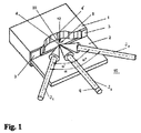
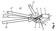
図3および4に、同じく本方法のための好ましい調製態様をなすワイヤシャドウ法の装置を示した。同図に、見やすいよう試料1を若干回転した2つの異なる図面を示した。
FIGS. 3 and 4 also show a wire shadow process apparatus that is also a preferred preparation for the process. The figure shows two different drawings in which the
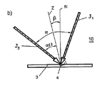
被検体は、長さlおよび厚さdの長い被検体1が得られるよう、例えば、ダイアモンドソーによって、試料材料から切出す。マイクロエレクロニクスウェーハから切出した試料が対象である場合、この試料1は、更に被覆層または層系(図示してない)を含むことができる構造(パタン)化表面3を有する。予設定した小さい径のワイヤまたはファイバ7を、例えば、接着剤で、試料表面3に固定する。通常、約100μm又はそれより小さく10μmまでの試料幅dを選択する。張付けるべきファイバは、径が試料幅dより小さく、マスクを形成する。さて、本発明にもとづき、少なくとも2つの、好ましくは,3つのイオンビームJを、好ましくは、試料表面3に直角に、投射ゾーン4のあるファイバ7へ向ける。この場合、垂線(法線)Nは、平面10内にある。平面10は、ワイヤの方向に平行に配置されるか、ないしは完全にワイヤ軸線を含んで(延在するよう)配される。
若干のエッチング時間後、試料1の材料切除によって、試料1の両側に、エッチング操作の終了時にTEMの観察表面20を形成するフランク6が構成される。更に、図3および4に示した如く、試料の櫛状尖端が構成されることも認められる。試料1は、試料の長さlに直角に見て(直角の断面において)明確なくさび状構造が生ずるよう、イオンビームJによって強くエッチングする。さて、試料1の両側のエッチングされたフランク6は、長い櫛を包含し、この櫛は、先細に推移し、試料縦方向に直角な矢印で示した如く、試料の側から、好ましくは、直角な観察方向12へ行われるTEM観察のために、上記範囲において電子透過性である。ファイバ7は、この状態において、同じく強くエッチングされる。
The specimen is cut out from the sample material by, for example, a diamond saw so that the
After some etching time, the
この場合も、斜切エッチングについて既に説明した如く、イオンビームによって、1種の円切片が、平面10内に形成され、イオンビームは、試料表面3へ向けて異なる角度で投射でき、或いはまた、全体として傾斜状態に配置できる。この場合、形成された円切片は、10°〜180°の範囲、好ましくは、30°〜140°の範囲の角度αをなせば有利であり、すべてのイオンビームは、上記円切片の上記イオンビームによって形成された平面10内にある。イオンビームの数に応じて、上述の最大角度をなし円切片を画成する2つのイオンビームによって閉じられた円切片内に、更なるイオンビームも存在する。イオンビームは、図5(a)−5(c)に模式的に示した如く、試料表面の垂線(法線)Nに関して対称にまたは非対称に配列できる。このように構成された上記円切片の中心軸線Zは、所望のエッチング操作を更に調節するため、上記垂線Nに対して角度βだけ傾斜させることもできる。この場合、角度βは、±20°の範囲、好ましくは、±10°の範囲にある。
In this case as well, as already explained for the oblique cutting, a kind of circular section is formed in the
図5(a)〜(b)に、共通の平面(10)内にあり試料表面に導かれるイオンビームJの可能な各位置および入射方向を示した。図5(a)において、角度αをなす2つのイオンビームJ1,J2によって形成された円切片の中心の対称軸線Zは、試料表面3の垂線N上にあり、この場合、すべてのイオンビームJの投射ゾーン4は、上記垂線上にあり、1種の交点として上記垂線に統合される。この対称的配置の場合、双方のイオンビームJ1,J2は、中心軸線Zまたは垂線Nに対して、投射ゾーンの方向へ角度α/2をもって導かれる。第3のイオンビームJ3を使用した場合、このイオンビームは、 円切片を包含する双方の外側イオンビームJ1,J2に対して角度α´、α´´をなす。更なるイオンビームは、円切片内に設置できる。円切片は、中心軸線Zが垂線Nに対して角度βだけ傾斜するよう配置でき、即ち、図5(b)に示した如く、対応する非対称性を有する。すべてのイオンビームが垂線Nの1つの側に位置することになる傾斜状態を図5(c)に示した。これらの配置は、3つのすべての事例に適し、更に、斜切エッチング法およびワイヤシャドウ法に特に適する。
FIGS. 5A to 5B show each possible position and incident direction of the ion beam J which is in the common plane (10) and is guided to the sample surface. In FIG. 5A, the axis of symmetry Z at the center of the circular slice formed by the two ion beams J1 and J2 forming the angle α is on the normal line N of the
平面10内にない標準TEM試料の加工のための少なくとも3つのイオンビームJの配置のため、3つのイオンビームJ1−J3は、図6(a)〜(c)に示した如く、投射ゾーン4に先端がある対応する角度αをなして円錐面11上にあるよう導かれる。円錐中心軸線Zの角度βだけ全装置を傾斜する方式は、図6(a)〜(c)にもとづく1つの平面内の先行の構成と類似である。3つよりも多数のイオンビームの場合、これらのイオンビームは、より小さい角度差で円錐体内にある。
Because of the arrangement of at least three ion beams J for processing a standard TEM sample that is not in the
投射ゾーン4の範囲内の少なくとも2つのイオンビームJの各種の関連性を上面図である図7(a)〜(d)に示した。横断面qのイオンビームは、すべて、同一平面10内にあり、少なくとも図示7(a)の表示に対応して投射ゾーン内で接触する。これらイオンビームは、すべて、投射ゾーン4と交差する平面10内の直線上にある。これらイオンビームは、図7(b)に示した如く、個々に重畳でき、または、図7(c)に示した如く、すべて重畳でき、または、図7(d)に示した如く、接触、重畳できる。
Various relevances of at least two ion beams J within the
図8(a)〜(d)に、少なくとも円錐面上または円錐面の間にあるイオンビームJの投射ゾーン4内の少なくとも3つのイオンビームJの関連性を示した。図8(a)に、投射ゾーン4内で接触する3つのイオンビームJ1〜J3を示した。図8(b)に、部分的に重畳する3つのイオンビームを示した。図8(c)に、互いに重畳する3つのイオンビームを示し、図8(d)に、重畳、接触する4つのイオンビームを示した。
8A to 8D show the relevance of at least three ion beams J in the
1 試料
3 試料表面
4 投射ゾーン
12 観察装置
20 観察表面
J イオンビーム
α (イオンビームの)相互角度
1
Claims (22)
少なくとも3つのイオンビーム(J1,J2,J3)がこれらの横断面で見て、試料表面(3)において互いに接触するおよび/または部分的に重畳して上記試料表面に投射ゾーン(4)を形成するよう、少なくとも3つの不動のイオンビーム(J1,J2,J3)を所定の角度(α)で相互に配向して試料表面(3)に導き、該イオンビーム(J1,J2,J3)は1つの平面内にあり、
試料(1)も該イオンビーム(J1,J2,J3)も、イオンエッチング中には移動されず、かくて、位置不変の状態で処理されることを特徴とする方法。 The sample is cut out from the solid material, and the sample surface (3) formed on the sample is treated with the ion beam (J) at a predetermined incident angle, and thus the projection zone (4) of the ion beam (J) of the sample (1). The material is excised from the sample surface (3) by ion etching until the desired observation surface (20) capable of realizing the observation (12) of the desired range of the sample (1) by the electron microscope is exposed in the range of In the method of preparing the sample for electron microscope examination (1),
At least three ion beams (J 1, J 2, J 3) are seen in these cross-sections and come into contact with each other and / or partially overlap on the sample surface (3) to form a projection zone (4) on the sample surface. Thus, at least three stationary ion beams (J1, J2, J3) are mutually oriented at a predetermined angle (α) and guided to the sample surface (3), and the ion beam (J1, J2, J3) is 1 In one plane,
Neither the sample (1) nor the ion beam (J1, J2, J3) is moved during ion etching and is thus processed in a position-invariant state.
その範囲に、イオンビーム(J1,J2,J3)の投射ゾーン(4)が位置し、イオンビームが、境界線が位置する平面(10)を形成し、
この平面(10)が、マスク(2)の表面に対して0°〜10°の範囲に若干傾斜して配置されると共に、マスク(2)の表面が、試料表面(3)に対して直角に配置されることを特徴とする請求項2の方法。 In the case of ion beam oblique cutting, a mask (2) having a flat surface in contact with the sample surface (3) with an interval in the range of 10 μm to 100 μm is used, so that both surfaces have a boundary line in the above range. Forming,
In that range, the projection zone (4) of the ion beam (J1, J2, J3) is located, and the ion beam forms a plane (10) on which the boundary line is located,
The plane (10) is arranged with a slight inclination in the range of 0 ° to 10 ° with respect to the surface of the mask (2), and the surface of the mask (2) is perpendicular to the sample surface (3). 3. The method of claim 2, wherein
Applications Claiming Priority (3)
| Application Number | Priority Date | Filing Date | Title |
|---|---|---|---|
| CH358/07 | 2007-03-06 | ||
| CH3582007 | 2007-03-06 | ||
| PCT/CH2008/000085 WO2008106815A2 (en) | 2007-03-06 | 2008-03-03 | Method for the production of a sample for electron microscopy |
Publications (3)
| Publication Number | Publication Date |
|---|---|
| JP2010520465A JP2010520465A (en) | 2010-06-10 |
| JP2010520465A5 JP2010520465A5 (en) | 2011-01-13 |
| JP5249955B2 true JP5249955B2 (en) | 2013-07-31 |
Family
ID=38042823
Family Applications (1)
| Application Number | Title | Priority Date | Filing Date |
|---|---|---|---|
| JP2009552039A Active JP5249955B2 (en) | 2007-03-06 | 2008-03-03 | Electron microscope specimen preparation method |
Country Status (4)
| Country | Link |
|---|---|
| US (1) | US8168960B2 (en) |
| EP (1) | EP2132550B1 (en) |
| JP (1) | JP5249955B2 (en) |
| WO (1) | WO2008106815A2 (en) |
Families Citing this family (13)
| Publication number | Priority date | Publication date | Assignee | Title |
|---|---|---|---|---|
| GB201002645D0 (en) | 2010-02-17 | 2010-03-31 | Univ Lancaster | Method and apparatus for ion beam polishing |
| AT509608B1 (en) | 2010-12-23 | 2011-10-15 | Leica Mikrosysteme Gmbh | DEVICE AND METHOD FOR COOLING SAMPLES DURING ONE ION BEAM PREPARATION |
| AT510606B1 (en) | 2011-02-09 | 2012-05-15 | Leica Mikrosysteme Gmbh | DEVICE AND METHOD FOR SAMPLE PREPARATION |
| DE102011111190A1 (en) * | 2011-08-25 | 2013-02-28 | Fraunhofer-Gesellschaft zur Förderung der angewandten Forschung e.V. | Method and device for preparing a sample for microstructural diagnostics |
| JP2013243307A (en) * | 2012-05-22 | 2013-12-05 | Toshiba Corp | Semiconductor manufacturing apparatus and semiconductor device manufacturing method |
| DE102013012225A1 (en) * | 2013-07-23 | 2015-01-29 | Carl Zeiss Microscopy Gmbh | Method for TEM lamella fabrication and assembly for TEM lamellae protection device |
| CN103792123B (en) * | 2014-02-25 | 2016-01-27 | 山西太钢不锈钢股份有限公司 | A kind of preparation method of steel samples used for transmission electron microscope observation |
| US10354836B2 (en) * | 2014-03-09 | 2019-07-16 | Ib Labs, Inc. | Methods, apparatuses, systems and software for treatment of a specimen by ion-milling |
| US9911573B2 (en) | 2014-03-09 | 2018-03-06 | Ib Labs, Inc. | Methods, apparatuses, systems and software for treatment of a specimen by ion-milling |
| DE102015219298B4 (en) * | 2015-10-06 | 2019-01-24 | Fraunhofer-Gesellschaft zur Förderung der angewandten Forschung e.V. | Method for preparing a sample for microstructural diagnostics and sample for microstructure diagnostics |
| CN105699149A (en) * | 2016-04-05 | 2016-06-22 | 工业和信息化部电子第五研究所 | Layer stripping method in chip failure analysis process |
| US10417881B2 (en) * | 2016-05-02 | 2019-09-17 | Norman R. Byrne | Wireless status indicator light |
| KR20220103161A (en) | 2020-01-29 | 2022-07-21 | 주식회사 히타치하이테크 | ion milling device |
Family Cites Families (15)
| Publication number | Priority date | Publication date | Assignee | Title |
|---|---|---|---|---|
| JPS6064228A (en) * | 1983-09-20 | 1985-04-12 | Nec Corp | Method and apparatus for preparing sample for transmission type electron microscope |
| US5009743A (en) * | 1989-11-06 | 1991-04-23 | Gatan Incorporated | Chemically-assisted ion beam milling system for the preparation of transmission electron microscope specimens |
| US5825035A (en) * | 1993-03-10 | 1998-10-20 | Hitachi, Ltd. | Processing method and apparatus using focused ion beam generating means |
| JPH0817800A (en) * | 1994-06-29 | 1996-01-19 | Hitachi Ltd | Focused ion beam apparatus and sample processing method using it |
| US5472566A (en) * | 1994-11-14 | 1995-12-05 | Gatan, Inc. | Specimen holder and apparatus for two-sided ion milling system |
| DE29507225U1 (en) * | 1995-04-29 | 1995-07-13 | Gruenewald Wolfgang Dr Rer Nat | Ion beam preparation device for electron microscopy |
| JP2001077058A (en) * | 1999-09-08 | 2001-03-23 | Seiko Instruments Inc | Machining method using convergent ion beam |
| US6768110B2 (en) * | 2000-06-21 | 2004-07-27 | Gatan, Inc. | Ion beam milling system and method for electron microscopy specimen preparation |
| JP4178741B2 (en) * | 2000-11-02 | 2008-11-12 | 株式会社日立製作所 | Charged particle beam apparatus and sample preparation apparatus |
| US7053370B2 (en) * | 2001-10-05 | 2006-05-30 | Canon Kabushiki Kaisha | Information acquisition apparatus, cross section evaluating apparatus, cross section evaluating method, and cross section working apparatus |
| US7002152B2 (en) * | 2003-02-15 | 2006-02-21 | Bal-Tec Ag | Sample preparation for transmission electron microscopy |
| US20040222082A1 (en) * | 2003-05-05 | 2004-11-11 | Applied Materials, Inc. | Oblique ion milling of via metallization |
| US6784427B1 (en) | 2003-07-31 | 2004-08-31 | Bal-Tec Ag | Samples for transmission electron microscopy |
| US20060017016A1 (en) * | 2004-07-01 | 2006-01-26 | Fei Company | Method for the removal of a microscopic sample from a substrate |
| JP4878135B2 (en) * | 2005-08-31 | 2012-02-15 | エスアイアイ・ナノテクノロジー株式会社 | Charged particle beam apparatus and sample processing method |
-
2008
- 2008-03-03 US US12/529,849 patent/US8168960B2/en active Active
- 2008-03-03 WO PCT/CH2008/000085 patent/WO2008106815A2/en active Application Filing
- 2008-03-03 JP JP2009552039A patent/JP5249955B2/en active Active
- 2008-03-03 EP EP08748344A patent/EP2132550B1/en active Active
Also Published As
| Publication number | Publication date |
|---|---|
| WO2008106815A3 (en) | 2008-10-23 |
| JP2010520465A (en) | 2010-06-10 |
| US20100025577A1 (en) | 2010-02-04 |
| US8168960B2 (en) | 2012-05-01 |
| EP2132550A2 (en) | 2009-12-16 |
| WO2008106815A2 (en) | 2008-09-12 |
| EP2132550B1 (en) | 2012-11-07 |
Similar Documents
| Publication | Publication Date | Title |
|---|---|---|
| JP5249955B2 (en) | Electron microscope specimen preparation method | |
| JP5033314B2 (en) | Ion beam processing apparatus and processing method | |
| JP5927380B2 (en) | TEM flake, manufacturing process thereof, and apparatus for executing the process | |
| JP2004245841A (en) | Temfib sample, and method of manufacturing the same | |
| JP2013257317A5 (en) | ||
| KR101757673B1 (en) | Method and device for the preparation of a sample for microstructure diagnostics | |
| JP2013257317A (en) | Lamella creation method and device using fixed-angle beam and rotating sample stage | |
| KR100796829B1 (en) | Tem sample slicing process | |
| JP2015159108A (en) | Charged particle beam device and sample observation method | |
| JP2007108105A (en) | Method for preparing sample for electron microscope, converged ion beam device and a sample support stand | |
| JP2010520465A5 (en) | ||
| JP6974820B2 (en) | Charged particle beam device, sample processing method | |
| JP6738257B2 (en) | Method for preparing sample for fine structure diagnosis and sample for fine structure diagnosis | |
| JP2002148159A (en) | Sample preparation method and device for it | |
| US20050082475A1 (en) | Methods for preparing samples for atom probe analysis | |
| TW201510499A (en) | Method of specimen processing in an apparatus with two or more particle beams and apparatus for this processing | |
| JPH11108813A (en) | Method and device for preparing sample | |
| JP5117764B2 (en) | Charged particle beam processing equipment | |
| EP2743026B1 (en) | Method of processing a material-specimen | |
| JP2011222426A (en) | Composite charged particle beam device | |
| US10832918B2 (en) | Method for removal of matter | |
| JPH08304243A (en) | Sample having cross sectional thin-film, its manufacture, and its holder | |
| JP4845452B2 (en) | Sample observation method and charged particle beam apparatus | |
| CN111065907B (en) | Sample manufacturing device and sample sheet manufacturing method | |
| JPH11258129A (en) | Method for making sample by focused ion beam |
Legal Events
| Date | Code | Title | Description |
|---|---|---|---|
| A521 | Request for written amendment filed |
Free format text: JAPANESE INTERMEDIATE CODE: A523 Effective date: 20101117 |
|
| A621 | Written request for application examination |
Free format text: JAPANESE INTERMEDIATE CODE: A621 Effective date: 20101117 |
|
| A131 | Notification of reasons for refusal |
Free format text: JAPANESE INTERMEDIATE CODE: A131 Effective date: 20120313 |
|
| A977 | Report on retrieval |
Free format text: JAPANESE INTERMEDIATE CODE: A971007 Effective date: 20120315 |
|
| A521 | Request for written amendment filed |
Free format text: JAPANESE INTERMEDIATE CODE: A523 Effective date: 20120611 |
|
| A131 | Notification of reasons for refusal |
Free format text: JAPANESE INTERMEDIATE CODE: A131 Effective date: 20121002 |
|
| A601 | Written request for extension of time |
Free format text: JAPANESE INTERMEDIATE CODE: A601 Effective date: 20121219 |
|
| A602 | Written permission of extension of time |
Free format text: JAPANESE INTERMEDIATE CODE: A602 Effective date: 20121227 |
|
| A521 | Request for written amendment filed |
Free format text: JAPANESE INTERMEDIATE CODE: A523 Effective date: 20130222 |
|
| TRDD | Decision of grant or rejection written | ||
| A01 | Written decision to grant a patent or to grant a registration (utility model) |
Free format text: JAPANESE INTERMEDIATE CODE: A01 Effective date: 20130319 |
|
| A61 | First payment of annual fees (during grant procedure) |
Free format text: JAPANESE INTERMEDIATE CODE: A61 Effective date: 20130412 |
|
| R150 | Certificate of patent or registration of utility model |
Free format text: JAPANESE INTERMEDIATE CODE: R150 Ref document number: 5249955 Country of ref document: JP Free format text: JAPANESE INTERMEDIATE CODE: R150 |
|
| FPAY | Renewal fee payment (event date is renewal date of database) |
Free format text: PAYMENT UNTIL: 20160419 Year of fee payment: 3 |
|
| R250 | Receipt of annual fees |
Free format text: JAPANESE INTERMEDIATE CODE: R250 |
|
| R250 | Receipt of annual fees |
Free format text: JAPANESE INTERMEDIATE CODE: R250 |
|
| R250 | Receipt of annual fees |
Free format text: JAPANESE INTERMEDIATE CODE: R250 |
|
| R250 | Receipt of annual fees |
Free format text: JAPANESE INTERMEDIATE CODE: R250 |
|
| R250 | Receipt of annual fees |
Free format text: JAPANESE INTERMEDIATE CODE: R250 |
|
| R250 | Receipt of annual fees |
Free format text: JAPANESE INTERMEDIATE CODE: R250 |
|
| R250 | Receipt of annual fees |
Free format text: JAPANESE INTERMEDIATE CODE: R250 |
|
| R250 | Receipt of annual fees |
Free format text: JAPANESE INTERMEDIATE CODE: R250 |