EP2107613A1 - Thin film transistor, method of fabricating the same, and organic lighting emitting diode display device including the same - Google Patents
Thin film transistor, method of fabricating the same, and organic lighting emitting diode display device including the same Download PDFInfo
- Publication number
- EP2107613A1 EP2107613A1 EP09156279A EP09156279A EP2107613A1 EP 2107613 A1 EP2107613 A1 EP 2107613A1 EP 09156279 A EP09156279 A EP 09156279A EP 09156279 A EP09156279 A EP 09156279A EP 2107613 A1 EP2107613 A1 EP 2107613A1
- Authority
- EP
- European Patent Office
- Prior art keywords
- semiconductor layer
- layer
- insulating layer
- body contact
- source
- Prior art date
- Legal status (The legal status is an assumption and is not a legal conclusion. Google has not performed a legal analysis and makes no representation as to the accuracy of the status listed.)
- Granted
Links
Images





Classifications
-
- H—ELECTRICITY
- H10—SEMICONDUCTOR DEVICES; ELECTRIC SOLID-STATE DEVICES NOT OTHERWISE PROVIDED FOR
- H10D—INORGANIC ELECTRIC SEMICONDUCTOR DEVICES
- H10D30/00—Field-effect transistors [FET]
- H10D30/60—Insulated-gate field-effect transistors [IGFET]
- H10D30/67—Thin-film transistors [TFT]
- H10D30/6704—Thin-film transistors [TFT] having supplementary regions or layers in the thin films or in the insulated bulk substrates for controlling properties of the device
- H10D30/6708—Thin-film transistors [TFT] having supplementary regions or layers in the thin films or in the insulated bulk substrates for controlling properties of the device for preventing the kink effect or the snapback effect, e.g. discharging the minority carriers of the channel region for preventing bipolar effect
- H10D30/6711—Thin-film transistors [TFT] having supplementary regions or layers in the thin films or in the insulated bulk substrates for controlling properties of the device for preventing the kink effect or the snapback effect, e.g. discharging the minority carriers of the channel region for preventing bipolar effect by using electrodes contacting the supplementary regions or layers
-
- H—ELECTRICITY
- H10—SEMICONDUCTOR DEVICES; ELECTRIC SOLID-STATE DEVICES NOT OTHERWISE PROVIDED FOR
- H10D—INORGANIC ELECTRIC SEMICONDUCTOR DEVICES
- H10D30/00—Field-effect transistors [FET]
- H10D30/01—Manufacture or treatment
- H10D30/021—Manufacture or treatment of FETs having insulated gates [IGFET]
- H10D30/031—Manufacture or treatment of FETs having insulated gates [IGFET] of thin-film transistors [TFT]
- H10D30/0312—Manufacture or treatment of FETs having insulated gates [IGFET] of thin-film transistors [TFT] characterised by the gate electrodes
- H10D30/0314—Manufacture or treatment of FETs having insulated gates [IGFET] of thin-film transistors [TFT] characterised by the gate electrodes of lateral top-gate TFTs comprising only a single gate
-
- H—ELECTRICITY
- H10—SEMICONDUCTOR DEVICES; ELECTRIC SOLID-STATE DEVICES NOT OTHERWISE PROVIDED FOR
- H10D—INORGANIC ELECTRIC SEMICONDUCTOR DEVICES
- H10D30/00—Field-effect transistors [FET]
- H10D30/01—Manufacture or treatment
- H10D30/021—Manufacture or treatment of FETs having insulated gates [IGFET]
- H10D30/031—Manufacture or treatment of FETs having insulated gates [IGFET] of thin-film transistors [TFT]
- H10D30/0321—Manufacture or treatment of FETs having insulated gates [IGFET] of thin-film transistors [TFT] comprising silicon, e.g. amorphous silicon or polysilicon
-
- H—ELECTRICITY
- H10—SEMICONDUCTOR DEVICES; ELECTRIC SOLID-STATE DEVICES NOT OTHERWISE PROVIDED FOR
- H10D—INORGANIC ELECTRIC SEMICONDUCTOR DEVICES
- H10D30/00—Field-effect transistors [FET]
- H10D30/60—Insulated-gate field-effect transistors [IGFET]
- H10D30/67—Thin-film transistors [TFT]
- H10D30/6704—Thin-film transistors [TFT] having supplementary regions or layers in the thin films or in the insulated bulk substrates for controlling properties of the device
- H10D30/6713—Thin-film transistors [TFT] having supplementary regions or layers in the thin films or in the insulated bulk substrates for controlling properties of the device characterised by the properties of the source or drain regions, e.g. compositions or sectional shapes
-
- H—ELECTRICITY
- H10—SEMICONDUCTOR DEVICES; ELECTRIC SOLID-STATE DEVICES NOT OTHERWISE PROVIDED FOR
- H10D—INORGANIC ELECTRIC SEMICONDUCTOR DEVICES
- H10D86/00—Integrated devices formed in or on insulating or conducting substrates, e.g. formed in silicon-on-insulator [SOI] substrates or on stainless steel or glass substrates
- H10D86/40—Integrated devices formed in or on insulating or conducting substrates, e.g. formed in silicon-on-insulator [SOI] substrates or on stainless steel or glass substrates characterised by multiple TFTs
-
- H—ELECTRICITY
- H10—SEMICONDUCTOR DEVICES; ELECTRIC SOLID-STATE DEVICES NOT OTHERWISE PROVIDED FOR
- H10D—INORGANIC ELECTRIC SEMICONDUCTOR DEVICES
- H10D86/00—Integrated devices formed in or on insulating or conducting substrates, e.g. formed in silicon-on-insulator [SOI] substrates or on stainless steel or glass substrates
- H10D86/01—Manufacture or treatment
- H10D86/021—Manufacture or treatment of multiple TFTs
- H10D86/0221—Manufacture or treatment of multiple TFTs comprising manufacture, treatment or patterning of TFT semiconductor bodies
- H10D86/0223—Manufacture or treatment of multiple TFTs comprising manufacture, treatment or patterning of TFT semiconductor bodies comprising crystallisation of amorphous, microcrystalline or polycrystalline semiconductor materials
- H10D86/0225—Manufacture or treatment of multiple TFTs comprising manufacture, treatment or patterning of TFT semiconductor bodies comprising crystallisation of amorphous, microcrystalline or polycrystalline semiconductor materials using crystallisation-promoting species, e.g. using a Ni catalyst
Definitions
- aspects of the present invention relate to a thin film transistor, a method of fabricating the same, and an organic light emitting diode display device including the same.
- a polycrystalline silicon layer is widely used as a semiconductor layer of a thin film transistor, because of its high field effect mobility and its applicability to a highspeed circuit and/or a complementary metal-oxide semiconductor (CMOS) circuit.
- CMOS complementary metal-oxide semiconductor
- a thin film transistor using such a polycrystalline silicon layer is used as a switching device of an active matrix liquid crystal display (AMLCD) device.
- AMLCD active matrix liquid crystal display
- Such a thin film transistor is also used as a switching device and/or a driving device of an active matrix organic light emitting diode display device (AMOLED).
- AMOLED active matrix organic light emitting diode display device
- the polycrystalline silicon thin film transistor used in the active matrix display devices is generally a floating body polycrystalline silicon thin film transistor (poly-Si TFT) having a floating, island-shaped semiconductor layer. As a floating body polycrystalline silicon thin film transistor is scaled down, it leads to a reduced drain current and a reduced saturation region thereof.
- poly-Si TFT floating body polycrystalline silicon thin film transistor
- a gate-body contact TFT in which a semiconductor layer is connected with a gate electrode, has been proposed.
- the gate-body contact TFT has an enhanced sub-threshold slope value and a high drain current at a low gate voltage. Accordingly, an on/off characteristic can be achieved, even at such a low gate voltage, resulting in a low-power, flat panel display device.
- a body contact region that contacts a gate electrode was separately formed, so as to extend from a conventional semiconductor layer having no body contact region, in order to implement a gate-body contact thin film transistor.
- this configuration increases an area occupied by a semiconductor layer and the body contact region, and is inappropriate for device integration.
- aspects of the present invention provide a thin film transistor having a smaller area than a conventional gate-body contact thin film transistor, by implementing a gate-body contact structure, without extending a separate body contact region from a semiconductor layer, by using an edge region of a semiconductor layer as a body contact region.
- aspects of the present invention also relate to a method of fabricating the thin film transistor, and an organic light emitting diode display device including the same.
- a thin film transistor includes: a substrate; a semiconductor layer disposed on the substrate and including a channel region, source/drain regions, and a body contact region; a gate insulating layer disposed on the semiconductor layer and exposing the body contact region; a gate electrode disposed on the gate insulating layer, in contact with the body contact region; an interlayer insulating layer disposed on the gate electrode; and source/drain electrodes disposed on the interlayer insulating layer and electrically connected to the source/drain regions.
- the body contact region is disposed at an edge of the semiconductor layer.
- a method of fabricating a thin film transistor includes: forming a semiconductor layer on a substrate; forming a gate insulating layer on the semiconductor layer, which exposes an edge of the semiconductor layer; forming a gate electrode on the gate insulating layer, which contacts the exposed edge of the semiconductor layer; forming an interlayer insulating layer on the gate electrode; and forming source/drain electrodes on the interlayer insulating layer.
- the source/drain electrodes are electrically connected to source/drain regions of the semiconductor layer, through openings in the interlayer insulating layer and the gate insulating layer.
- an organic lighting emitting diode display device includes: a substrate; a semiconductor layer disposed on the substrate and including a channel region, source/drain regions, and a body contact region; a gate insulating layer disposed on the semiconductor layer and exposing the body contact region; a gate electrode disposed on the gate insulating layer, in contact with the body contact region; an interlayer insulating layer disposed on the gate electrode; source/drain electrodes disposed on the interlayer insulating layer and electrically connected to the source/drain regions; a first electrode electrically connected to one of the source/drain electrodes; an organic layer disposed on the first electrode and including an emission layer; and a second electrode disposed on the organic layer.
- the body contact region is disposed at an edge of the semiconductor layer.
- first element when a first element is said to be disposed or formed "on”, or “adjacent to”, a second element, the first element can directly contact the second element, or can be separated from the second element by one or more other elements located therebetween.
- first element when an element is referred to as being disposed or formed "directly on” another element, there are no intervening elements present.
- the term "and/or" includes any and all combinations of one or more of the associated listed items.
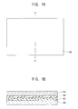
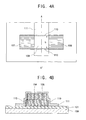
- FIGS. 1A , 2A , 3A , 4A , and 5A are plan views illustrating a process of fabricating a thin film transistor, according to Exemplary Embodiment 1 of the present invention.
- FIGS.1 B , 2B , 3B , 4B , and 5B are cross-sectional views taken along line A-A' of FIGS. 1A , 2A , 3A , 4A , and 5A .
- a buffer layer 101 is formed on a substrate 100, which can be formed of glass or plastic.
- the buffer layer 101 can include one or more insulating layers, such as a silicon oxide layer, or a silicon nitride layer.
- the insulating layers can be formed by chemical vapor deposition or physical vapor deposition, for example.
- the buffer layer 101 prevents the diffusion of moisture and/or impurities from the substrate 100.
- the buffer layer 101 can also be used to control the rate of heat transfer during the crystallization of an amorphous silicon layer.
- a polycrystalline silicon layer 102 is then formed on the buffer layer 101.
- the polycrystalline silicon layer 102 may be formed by crystallizing an amorphous silicon layer, using a crystallization method, such as Rapid Thermal Annealing (RTA), Solid Phase Crystallization (SPC), Excimer Laser Crystallization (ELA), Metal Induced Crystallization (MIC), Metal Induced Lateral Crystallization (MILC), Sequential Lateral Solidification (SLS), or Super Grain Silicon (SGS).
- RTA Rapid Thermal Annealing
- SPC Solid Phase Crystallization
- ELA Excimer Laser Crystallization
- MIC Metal Induced Crystallization
- MILC Metal Induced Lateral Crystallization
- SLS Sequential Lateral Solidification
- SGS Super Grain Silicon
- the insulating layer 103 is then formed on the polycrystalline silicon layer 102.
- the insulating layer 103 may be a silicon oxide layer, a silicon nitride layer, or a combination thereof.
- the polycrystalline silicon layer 102 and the insulating layer 103 are patterned.
- the polycrystalline silicon layer 102 is patterned to form a semiconductor layer 104.
- the insulating layer 103 is patterned to form a gate insulating layer 105.
- the gate insulating layer 105 exposes one or more edge regions 106 of the semiconductor layer 104.
- the length of the semiconductor layer 104 refers to a direction that is parallel to a line connecting a source region 107 ( FIG. 3A ) to a drain region 108 ( FIG. 3A ) of the semiconductor layer 104
- the width of the semiconductor layer 104 refers to a direction perpendicular to the length direction, i.e., extending along line A-A'.
- the edge regions 106 of the semiconductor layer 104 are separated by a predetermined distance, across the width of the semiconductor layer 104.
- the gate insulating layer 105 may be formed to expose the edge region 106 of the semiconductor layer 104, by a one-time patterning process, i.e., by adjusting etching conditions so that the insulating layer 103 is over-etched relative to the polycrystalline silicon layer 102.
- the gate insulating layer 105 may be etched to expose the edge region 106 of the semiconductor layer 104, by making a critical dimension (CD) bias of the insulating layer 103 greater than that of the underlying polycrystalline silicon layer 102.
- CD critical dimension
- the width a of the edge region 106 is less than about 0.1 ⁇ m. This range forms a gate-body contact TFT structure without a separate extended body contact region, while not greatly reducing the area of a channel region of the existing semiconductor layer 104.
- an impurity is injected into the edge region 106 of the semiconductor layer 104, which is exposed through the gate insulating layer 105.
- a different type of impurity is injected into the source/drain regions 107 and 108 of the semiconductor layer 104.
- One of the impurities can be an N-type impurity, and the other impurity can be a P-type impurity, for example. This results in a PNP or NPN structure of the source/drain regions 107 and 108 of the semiconductor layer 104 and the edge region 106, such that current flowing from the source and/or drain regions 107 and 108 does not flow into the edge region 106.
- the P-type impurity can be selected from the group consisting of boron B, aluminum (Al), gallium (Ga), and indium (In).
- the N-type impurity can be selected from the group consisting of phosphorus (P), arsenic (As), and antimony (Sb).
- the source/drain regions 107 and 108 of the semiconductor layer 104 are formed by injecting an impurity into regions in which the source/drain regions 107 and 108 of the semiconductor layer 104 are to be formed.
- a channel region 109 is formed between the source region 107 and the drain region 108.
- Body contact regions 110 are formed in edge regions 106 of the semiconductor layer 104 and extend between the source region 107 and the drain region 108.
- the body contact regions 110 are connected to, and are disposed at opposing sides of, the channel region 109. For convenience, only one of the body contact regions 110 will be referred to hereinafter.
- the source/drain regions 107 and 108 may be formed by injecting the impurity into the semiconductor layer 104, using a photoresist pattern as a mask. Alternatively, the source/drain regions 107 and 108 may be formed by injecting the impurity into the semiconductor layer 104, using a subsequently formed gate electrode as a mask.
- a gate electrode material is deposited on the gate insulating layer 105 and is then patterned to form a gate electrode 111.
- the gate electrode 111 overlaps the channel region 109 and the body contact region 110.
- the gate electrode 111 may be a layer of aluminum (Al), a layer of an aluminum alloy such as aluminum-neodymium (Al-Nd), or multi-layers of an aluminum alloy stacked on a chromium (Cr) or molybdenum (Mo) alloy. Since the insulating layer 103 is patterned, so as to expose the body contact region 110, the gate electrode 111 contacts the body contact region 110, resulting in a gate-body contact TFT.
- the width b of the channel region 109 is smaller than the width of the semiconductor layer 104 as a whole, i.e., the channel region 109 plus the width of the body contact regions 110.
- a semiconductor layer is formed by forming a polycrystalline silicon layer on the entire surface of the substrate, forming a photoresist pattern on the polycrystalline silicon layer, and etching the polycrystalline silicon layer using the photoresist pattern as a mask.
- the edges of the semiconductor layer may be damaged by an etching solution or a plasma used for the etching.
- the photoresist remaining on the edges of the semiconductor layer may make the semiconductor layer non-uniform and/or have poor characteristics. This may affect a threshold voltage, or an S-factor, of a TFT including such a semiconductor layer, and may cause a hump on an I-V characteristic curve of the TFT. These problems are caused by including the damaged edges in the channel region.
- aspects of the present invention can solve the above and/or other problems, by injecting an impurity into edges of a semiconductor layer that contact a channel region, instead of including the edges in the channel region.
- the impurities form body contact regions, which contact a gate electrode. This makes it possible to form a gate-body contact thin film transistor using an existing semiconductor layer, without forming a separate body contact region.
- an interlayer insulating layer 112 is formed on the entire surface of the substrate 100.
- the interlayer insulating layer 112 may be a silicon nitride layer, a silicon oxide layer, or a multi-layer thereof.
- the interlayer insulating layer 112 and the gate insulating layer 105 are then etched to form contact holes 113, which expose the source/drain regions 107 and 108 of the semiconductor layer 104.
- Source/drain electrodes 114 and 115 are then connected to the source/drain regions 107 and 108, through the contact holes 113.
- the source/drain electrodes 114 and 115 may be formed of one of molybdenum (Mo), chromium (Cr), tungsten (W), aluminum-neodymium (Al-Nd), titanium (Ti), molybdenum tungsten (MoW), and aluminum (Al).
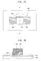
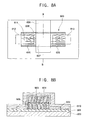
- FIGS. 6A , 7A , and 8A are plan views illustrating a process of fabricating a thin film transistor, according to Exemplary Embodiment 2 of the present invention.
- FIGS. 6B , 7B , and 8B are cross-sectional views taken along line B-B' of FIGS. 6A , 7A , and 8A .
- a buffer layer 601 is formed on a substrate 600, and then a polycrystalline silicon layer 602 is formed on the buffer layer 601.
- a polycrystalline silicon layer 602 is formed on the buffer layer 601.
- FIGS. 7A and 7B only the polycrystalline silicon layer 602 is patterned at first, to form a semiconductor layer 603, unlike Exemplary Embodiment 1.
- An insulating layer is deposited on the entire surface of the substrate 600.
- the insulating layer is patterned, thereby forming a gate insulating layer 604.
- the patterning of the gate insulating layer 604 exposes an edge of the semiconductor layer 603, which is connected to a channel region 607 of the semiconductor layer 603.
- a first impurity is then injected into the exposed edge of the semiconductor layer 603, to form a body contact region 608.
- a second impurity is injected into other portions of the semiconductor layer 603, to form a source region 605 and a drain region 606.
- the channel region 607 is an undoped portion of the semiconductor layer 603, which contacts the body contact region 608, and is disposed between the source and drain regions 605 and 606.
- the first and second impurities can be N-type or P-type impurities, so long as they are different types of impurities.
- the length c of the body contact region 608 may be equal to, or larger than, the length of the channel region 607.
- a gate electrode material is deposited on the gate insulating layer 604.
- the gate electrode material is then patterned to form a gate electrode 609 that overlaps the channel region 607 and the body contact region 608.
- the gate electrode 609 contacts the body contact region 608, through a hole formed when patterning the patterned gate insulating layer 604, resulting in a completed gate-body contact thin film transistor.
- An interlayer insulating layer 610 is formed on the entire surface of the substrate.
- the interlayer insulating layer 610 and the gate insulating layer 604 are then etched, to form contact holes 611 that expose the source/drain regions 605 and 606 of the semiconductor layer 603.
- Source/drain electrodes 612 and 613 are connected to the source/drain regions 605 and 606, through the contact holes 611.
- a process of gettering a crystallization inducing metal in the semiconductor layer, using the edge of the semiconductor layer, according to Exemplary Embodiment 3 of the present invention, will now be described.
- a crystallization inducing metal is used to crystallize the polycrystalline silicon layer into the semiconductor layers of Exemplary Embodiments 1 and 2.
- the gettering process refers to gettering the crystallization inducing metal remaining in a channel forming region into an exposed edge of a semiconductor layer, by performing an annealing process.
- the annealing process is performed after the impurity, and particularly an N-type impurity, is injected into the edge of the semiconductor layer.
- the gettering process using the exposed edge has a high gettering efficiency, because the crystallization inducing metal present in the channel region has to move only a short distance to reach the exposed edge.
- the annealing process is performed for from about 30 seconds to about 10 hours, at a temperature ranging from 450°C to 900°C.
- An annealing temperature lower than about 450°C may not sufficiently remove the crystallization inducing metal from a semiconductor layer.
- An annealing temperature exceeding 900°C may deform a substrate.
- An annealing time of less than 30 seconds may not sufficiently remove the crystallization induced metal.
- An annealing time exceeding 10 hours may deform the substrate, increase fabrication costs of a TFT, and reduce yields.
- FIG. 9 is a cross-sectional view of an organic light emitting diode display device including a TFT, according to an exemplary embodiment of the present invention.
- an insulating layer 116 is formed on the entire surface of the substrate 100 including the TFT, according to the exemplary embodiment of the present invention shown in FIG. 5B .
- the insulating layer 116 may be formed of an inorganic layer selected from a silicon oxide layer, a silicon nitride layer, a silicon on glass layer, or an organic layer selected from polyimide, benzocyclobutene series resin, or acrylate.
- the insulating layer 116 may include the inorganic layer and the organic layer in a stacked formation.
- the insulating layer 116 is etched to form a hole 117 that exposes one of the source and drain electrodes 114 and 115.
- a first electrode 118 is formed through the hole 117 and is connected to one of the source/drain electrodes 114 and 115.
- the first electrode 118 may an anode or a cathode.
- the first electrode 118 may be formed of a transparent conductive material, such as indium tin oxide (ITO), indium zinc oxide (IZO), or indium tin zinc oxide (ITZO).
- ITO indium tin oxide
- IZO indium zinc oxide
- ITZO indium tin zinc oxide
- the first electrode 118 is a cathode, it may be formed of Mg, Ca, Al, Ag, Ba, or an alloy thereof.
- a pixel definition layer 119 is then formed on the first electrode 118.
- the pixel definition layer 119 has an opening that exposes the surface of the first electrode 118.
- An organic layer 120 that includes an emission layer is formed on the first electrode 118.
- the organic layer 120 may further include at least one selected from the group consisting of a hole injection layer, a hole transport layer, a hole blocking layer, an electron blocking layer, an electron injection layer, and an electron transport layer.
- a second electrode 121 is then formed on the organic layer 120, to complete the organic light emitting diode display device.
- a thin film transistor has a smaller area than a conventional gate-body contact thin film transistor, due to implementing a body contact region that does not include a separate body contact region.
- the body contact region is formed from an edge region of a semiconductor layer.
Landscapes
- Thin Film Transistor (AREA)
- Electroluminescent Light Sources (AREA)
- Recrystallisation Techniques (AREA)
Abstract

Description
- Aspects of the present invention relate to a thin film transistor, a method of fabricating the same, and an organic light emitting diode display device including the same.
- In general, a polycrystalline silicon layer is widely used as a semiconductor layer of a thin film transistor, because of its high field effect mobility and its applicability to a highspeed circuit and/or a complementary metal-oxide semiconductor (CMOS) circuit. A thin film transistor using such a polycrystalline silicon layer is used as a switching device of an active matrix liquid crystal display (AMLCD) device. Such a thin film transistor is also used as a switching device and/or a driving device of an active matrix organic light emitting diode display device (AMOLED).
- The polycrystalline silicon thin film transistor used in the active matrix display devices is generally a floating body polycrystalline silicon thin film transistor (poly-Si TFT) having a floating, island-shaped semiconductor layer. As a floating body polycrystalline silicon thin film transistor is scaled down, it leads to a reduced drain current and a reduced saturation region thereof.
- To solve this problem, a gate-body contact TFT, in which a semiconductor layer is connected with a gate electrode, has been proposed. The gate-body contact TFT has an enhanced sub-threshold slope value and a high drain current at a low gate voltage. Accordingly, an on/off characteristic can be achieved, even at such a low gate voltage, resulting in a low-power, flat panel display device.
- Conventionally, a body contact region that contacts a gate electrode was separately formed, so as to extend from a conventional semiconductor layer having no body contact region, in order to implement a gate-body contact thin film transistor. However, this configuration increases an area occupied by a semiconductor layer and the body contact region, and is inappropriate for device integration.
- Aspects of the present invention provide a thin film transistor having a smaller area than a conventional gate-body contact thin film transistor, by implementing a gate-body contact structure, without extending a separate body contact region from a semiconductor layer, by using an edge region of a semiconductor layer as a body contact region. Aspects of the present invention also relate to a method of fabricating the thin film transistor, and an organic light emitting diode display device including the same.
- According to an exemplary embodiment of the present invention, a thin film transistor includes: a substrate; a semiconductor layer disposed on the substrate and including a channel region, source/drain regions, and a body contact region; a gate insulating layer disposed on the semiconductor layer and exposing the body contact region; a gate electrode disposed on the gate insulating layer, in contact with the body contact region; an interlayer insulating layer disposed on the gate electrode; and source/drain electrodes disposed on the interlayer insulating layer and electrically connected to the source/drain regions. The body contact region is disposed at an edge of the semiconductor layer.
- According to another exemplary embodiment of the present invention, a method of fabricating a thin film transistor includes: forming a semiconductor layer on a substrate; forming a gate insulating layer on the semiconductor layer, which exposes an edge of the semiconductor layer; forming a gate electrode on the gate insulating layer, which contacts the exposed edge of the semiconductor layer; forming an interlayer insulating layer on the gate electrode; and forming source/drain electrodes on the interlayer insulating layer. The source/drain electrodes are electrically connected to source/drain regions of the semiconductor layer, through openings in the interlayer insulating layer and the gate insulating layer.
- According to yet another exemplary embodiment of the present invention, an organic lighting emitting diode display device includes: a substrate; a semiconductor layer disposed on the substrate and including a channel region, source/drain regions, and a body contact region; a gate insulating layer disposed on the semiconductor layer and exposing the body contact region; a gate electrode disposed on the gate insulating layer, in contact with the body contact region; an interlayer insulating layer disposed on the gate electrode; source/drain electrodes disposed on the interlayer insulating layer and electrically connected to the source/drain regions; a first electrode electrically connected to one of the source/drain electrodes; an organic layer disposed on the first electrode and including an emission layer; and a second electrode disposed on the organic layer. The body contact region is disposed at an edge of the semiconductor layer.
- These and/or other aspects and advantages of the invention will become apparent and more readily appreciated from the following description of the exemplary embodiments, taken in conjunction with the accompanying drawings, of which:
-
FIGS. 1A ,2A ,3A ,4A , and5A are plan views illustrating a process of fabricating a thin film transistor, according to Exemplary Embodiment 1 of the present invention, andFIGS. 1B ,2B ,3B ,4B , and5B are cross-sectional views taken along line A-A' ofFIGS. 1A ,2A ,3A ,4A , and5A , respectively; -
FIGS. 6A ,7A and8A are plan views illustrating a process of fabricating a thin film transistor, according to Exemplary Embodiment 2 of the present invention, andFIGS. 6B ,7B and8B are cross-sectional views taken along line B-B' ofFIGS. 6A ,7A , and8A , respectively; and -
FIG. 9 is a cross-sectional view of an organic light emitting diode display device including a thin film transistor, according to an exemplary embodiment of the present invention. - Reference will now be made in detail to the exemplary embodiments of the present invention, examples of which are shown in the accompanying drawings, wherein like reference numerals refer to the like elements throughout the specification. The exemplary embodiments are described below, in order to explain the aspects of the present invention, by referring to the figures.
- As referred to herein, when a first element is said to be disposed or formed "on", or "adjacent to", a second element, the first element can directly contact the second element, or can be separated from the second element by one or more other elements located therebetween. In contrast, when an element is referred to as being disposed or formed "directly on" another element, there are no intervening elements present. As used herein, the term "and/or" includes any and all combinations of one or more of the associated listed items.
-
FIGS. 1A ,2A ,3A ,4A , and5A are plan views illustrating a process of fabricating a thin film transistor, according to Exemplary Embodiment 1 of the present invention.FIGS.1 B ,2B ,3B ,4B , and5B are cross-sectional views taken along line A-A' ofFIGS. 1A ,2A ,3A ,4A , and5A . - Referring to
FIGS. 1A and 1 B , abuffer layer 101 is formed on asubstrate 100, which can be formed of glass or plastic. Thebuffer layer 101 can include one or more insulating layers, such as a silicon oxide layer, or a silicon nitride layer. The insulating layers can be formed by chemical vapor deposition or physical vapor deposition, for example. Thebuffer layer 101 prevents the diffusion of moisture and/or impurities from thesubstrate 100. Thebuffer layer 101 can also be used to control the rate of heat transfer during the crystallization of an amorphous silicon layer. - A
polycrystalline silicon layer 102 is then formed on thebuffer layer 101. Thepolycrystalline silicon layer 102 may be formed by crystallizing an amorphous silicon layer, using a crystallization method, such as Rapid Thermal Annealing (RTA), Solid Phase Crystallization (SPC), Excimer Laser Crystallization (ELA), Metal Induced Crystallization (MIC), Metal Induced Lateral Crystallization (MILC), Sequential Lateral Solidification (SLS), or Super Grain Silicon (SGS). - An
insulating layer 103 is then formed on thepolycrystalline silicon layer 102. Theinsulating layer 103 may be a silicon oxide layer, a silicon nitride layer, or a combination thereof. - Referring to
FIGS. 2A and 2B , thepolycrystalline silicon layer 102 and theinsulating layer 103 are patterned. Thepolycrystalline silicon layer 102 is patterned to form asemiconductor layer 104. Theinsulating layer 103 is patterned to form agate insulating layer 105. Thegate insulating layer 105 exposes one ormore edge regions 106 of thesemiconductor layer 104. - Herein, the length of the
semiconductor layer 104 refers to a direction that is parallel to a line connecting a source region 107 (FIG. 3A ) to a drain region 108 (FIG. 3A ) of thesemiconductor layer 104, and the width of thesemiconductor layer 104 refers to a direction perpendicular to the length direction, i.e., extending along line A-A'. Theedge regions 106 of thesemiconductor layer 104 are separated by a predetermined distance, across the width of thesemiconductor layer 104. - The
gate insulating layer 105 may be formed to expose theedge region 106 of thesemiconductor layer 104, by a one-time patterning process, i.e., by adjusting etching conditions so that the insulatinglayer 103 is over-etched relative to thepolycrystalline silicon layer 102. For example, thegate insulating layer 105 may be etched to expose theedge region 106 of thesemiconductor layer 104, by making a critical dimension (CD) bias of the insulatinglayer 103 greater than that of the underlyingpolycrystalline silicon layer 102. - The width a of the
edge region 106 is less than about 0.1 µm. This range forms a gate-body contact TFT structure without a separate extended body contact region, while not greatly reducing the area of a channel region of the existingsemiconductor layer 104. - Referring to
FIGS. 3A and 3B , an impurity is injected into theedge region 106 of thesemiconductor layer 104, which is exposed through thegate insulating layer 105. A different type of impurity is injected into the source/drain regions semiconductor layer 104. One of the impurities can be an N-type impurity, and the other impurity can be a P-type impurity, for example. This results in a PNP or NPN structure of the source/drain regions semiconductor layer 104 and theedge region 106, such that current flowing from the source and/or drainregions edge region 106. The P-type impurity can be selected from the group consisting of boron B, aluminum (Al), gallium (Ga), and indium (In). The N-type impurity can be selected from the group consisting of phosphorus (P), arsenic (As), and antimony (Sb). - The source/
drain regions semiconductor layer 104 are formed by injecting an impurity into regions in which the source/drain regions semiconductor layer 104 are to be formed. Achannel region 109 is formed between thesource region 107 and thedrain region 108.Body contact regions 110 are formed inedge regions 106 of thesemiconductor layer 104 and extend between thesource region 107 and thedrain region 108. Thebody contact regions 110 are connected to, and are disposed at opposing sides of, thechannel region 109. For convenience, only one of thebody contact regions 110 will be referred to hereinafter. - The source/
drain regions semiconductor layer 104, using a photoresist pattern as a mask. Alternatively, the source/drain regions semiconductor layer 104, using a subsequently formed gate electrode as a mask. - Referring to
FIGS. 4A and 4B , a gate electrode material is deposited on thegate insulating layer 105 and is then patterned to form agate electrode 111. Thegate electrode 111 overlaps thechannel region 109 and thebody contact region 110. Thegate electrode 111 may be a layer of aluminum (Al), a layer of an aluminum alloy such as aluminum-neodymium (Al-Nd), or multi-layers of an aluminum alloy stacked on a chromium (Cr) or molybdenum (Mo) alloy. Since the insulatinglayer 103 is patterned, so as to expose thebody contact region 110, thegate electrode 111 contacts thebody contact region 110, resulting in a gate-body contact TFT. As thebody contact regions 110 are disposed at opposing edges of thechannel region 109, the width b of thechannel region 109 is smaller than the width of thesemiconductor layer 104 as a whole, i.e., thechannel region 109 plus the width of thebody contact regions 110. - In the related art, a semiconductor layer is formed by forming a polycrystalline silicon layer on the entire surface of the substrate, forming a photoresist pattern on the polycrystalline silicon layer, and etching the polycrystalline silicon layer using the photoresist pattern as a mask. In etching the polycrystalline silicon layer, the edges of the semiconductor layer may be damaged by an etching solution or a plasma used for the etching.
- In addition, the photoresist remaining on the edges of the semiconductor layer may make the semiconductor layer non-uniform and/or have poor characteristics. This may affect a threshold voltage, or an S-factor, of a TFT including such a semiconductor layer, and may cause a hump on an I-V characteristic curve of the TFT. These problems are caused by including the damaged edges in the channel region.
- Aspects of the present invention can solve the above and/or other problems, by injecting an impurity into edges of a semiconductor layer that contact a channel region, instead of including the edges in the channel region. The impurities form body contact regions, which contact a gate electrode. This makes it possible to form a gate-body contact thin film transistor using an existing semiconductor layer, without forming a separate body contact region.
- Referring to
FIGS. 5A and 5B , aninterlayer insulating layer 112 is formed on the entire surface of thesubstrate 100. The interlayer insulatinglayer 112 may be a silicon nitride layer, a silicon oxide layer, or a multi-layer thereof. - The interlayer insulating
layer 112 and thegate insulating layer 105 are then etched to form contact holes 113, which expose the source/drain regions semiconductor layer 104. Source/drain electrodes drain regions drain electrodes -
FIGS. 6A ,7A , and8A are plan views illustrating a process of fabricating a thin film transistor, according to Exemplary Embodiment 2 of the present invention.FIGS. 6B ,7B , and8B are cross-sectional views taken along line B-B' ofFIGS. 6A ,7A , and8A . - Referring to
FIGS. 6A and 6B , abuffer layer 601 is formed on asubstrate 600, and then apolycrystalline silicon layer 602 is formed on thebuffer layer 601. Referring toFIGS. 7A and 7B , only thepolycrystalline silicon layer 602 is patterned at first, to form asemiconductor layer 603, unlike Exemplary Embodiment 1. - An insulating layer is deposited on the entire surface of the
substrate 600. The insulating layer is patterned, thereby forming agate insulating layer 604. The patterning of thegate insulating layer 604 exposes an edge of thesemiconductor layer 603, which is connected to achannel region 607 of thesemiconductor layer 603. - A first impurity is then injected into the exposed edge of the
semiconductor layer 603, to form abody contact region 608. A second impurity is injected into other portions of thesemiconductor layer 603, to form asource region 605 and adrain region 606. Thechannel region 607 is an undoped portion of thesemiconductor layer 603, which contacts thebody contact region 608, and is disposed between the source and drainregions body contact region 608 may be equal to, or larger than, the length of thechannel region 607. - Referring to
FIGS. 8A and 8B , a gate electrode material is deposited on thegate insulating layer 604. The gate electrode material is then patterned to form agate electrode 609 that overlaps thechannel region 607 and thebody contact region 608. Thegate electrode 609 contacts thebody contact region 608, through a hole formed when patterning the patternedgate insulating layer 604, resulting in a completed gate-body contact thin film transistor. - An interlayer insulating
layer 610 is formed on the entire surface of the substrate. The interlayer insulatinglayer 610 and thegate insulating layer 604 are then etched, to form contact holes 611 that expose the source/drain regions semiconductor layer 603. Source/drain electrodes drain regions - A process of gettering a crystallization inducing metal in the semiconductor layer, using the edge of the semiconductor layer, according to Exemplary Embodiment 3 of the present invention, will now be described. A crystallization inducing metal is used to crystallize the polycrystalline silicon layer into the semiconductor layers of Exemplary Embodiments 1 and 2.
- The gettering process refers to gettering the crystallization inducing metal remaining in a channel forming region into an exposed edge of a semiconductor layer, by performing an annealing process. The annealing process is performed after the impurity, and particularly an N-type impurity, is injected into the edge of the semiconductor layer.
- Since the exposed edge contacts the channel region, the gettering process using the exposed edge has a high gettering efficiency, because the crystallization inducing metal present in the channel region has to move only a short distance to reach the exposed edge.
- The annealing process is performed for from about 30 seconds to about 10 hours, at a temperature ranging from 450°C to 900°C. An annealing temperature lower than about 450°C may not sufficiently remove the crystallization inducing metal from a semiconductor layer. An annealing temperature exceeding 900°C may deform a substrate. An annealing time of less than 30 seconds may not sufficiently remove the crystallization induced metal. An annealing time exceeding 10 hours may deform the substrate, increase fabrication costs of a TFT, and reduce yields.
-
FIG. 9 is a cross-sectional view of an organic light emitting diode display device including a TFT, according to an exemplary embodiment of the present invention. Referring toFIG. 9 , an insulatinglayer 116 is formed on the entire surface of thesubstrate 100 including the TFT, according to the exemplary embodiment of the present invention shown inFIG. 5B . The insulatinglayer 116 may be formed of an inorganic layer selected from a silicon oxide layer, a silicon nitride layer, a silicon on glass layer, or an organic layer selected from polyimide, benzocyclobutene series resin, or acrylate. The insulatinglayer 116 may include the inorganic layer and the organic layer in a stacked formation. - The insulating
layer 116 is etched to form ahole 117 that exposes one of the source and drainelectrodes first electrode 118 is formed through thehole 117 and is connected to one of the source/drain electrodes first electrode 118 may an anode or a cathode. When thefirst electrode 118 is an anode, it may be formed of a transparent conductive material, such as indium tin oxide (ITO), indium zinc oxide (IZO), or indium tin zinc oxide (ITZO). When thefirst electrode 118 is a cathode, it may be formed of Mg, Ca, Al, Ag, Ba, or an alloy thereof. - A
pixel definition layer 119 is then formed on thefirst electrode 118. Thepixel definition layer 119 has an opening that exposes the surface of thefirst electrode 118. Anorganic layer 120 that includes an emission layer is formed on thefirst electrode 118. Theorganic layer 120 may further include at least one selected from the group consisting of a hole injection layer, a hole transport layer, a hole blocking layer, an electron blocking layer, an electron injection layer, and an electron transport layer. Asecond electrode 121 is then formed on theorganic layer 120, to complete the organic light emitting diode display device. - A thin film transistor, according to aspects of the present invention, has a smaller area than a conventional gate-body contact thin film transistor, due to implementing a body contact region that does not include a separate body contact region. The body contact region is formed from an edge region of a semiconductor layer.
Claims (22)
- A thin film transistor comprising:a substrate (100);a semiconductor layer (104) disposed on the substrate (100), comprising a channel region, a source region (107), a drain region (108), and a first body contact region (110) that is formed in a first edge of the semiconductor layer (104);a gate insulating layer (105) disposed on the semiconductor layer (104), exposing the first body contact region (110);a gate electrode (111) disposed on the gate insulating layer (105), so as to contact the first body contact region (110);an interlayer insulating layer (112) disposed on the gate electrode (111); andsource (114) and drain (115) electrodes disposed on the interlayer insulating layer (112) and electrically connected to the source (107) and drain (108) regions, respectively.
- The thin film transistor of claim 1, wherein the first body contact region (110) is connected to the channel region.
- The thin film transistor of claims 1 or 2, wherein:the first body contact region (110) comprises a first type of impurity; andthe source (107) and drain (108) regions comprise a second type of impurity.
- The thin film transistor of claims 1 to 3, wherein the semiconductor layer (104) comprises a second body contact region (110) that opposes the first body contact region (110), and which is exposed by the gate insulating layer (105).
- The thin film transistor of claim 4, wherein:the second body contact region (110) comprises a first type of impurity; andthe source (107)/drain (108) regions comprise a second type of impurity.
- The thin film transistor of claim 4 or 5, wherein the first and second body contact regions (110) are disposed on opposing sides of the channel region and extend between the source (107) and drain (108) regions.
- The thin film transistor of claims 1 to 6, wherein the width of the gate insulating layer (105) corresponding to the channel region is smaller than the width of the semiconductor layer (104).
- The thin film transistor of claims 1 to 7, wherein the width of the body contact region (110) is not more than about 0.1 µm.
- The thin film transistor of claims 3 to 8, wherein:the first type of impurity is an N-type impurity;the second type of impurity is a P-type impurity; andthe semiconductor layer (104) is crystallized using a crystallization inducing metal.
- A method of fabricating a thin film transistor, the method comprising:forming a semiconductor layer (104) on a substrate (100);forming a gate insulating layer (105) on the semiconductor layer (104), so as to expose an edge of the semiconductor layer (104);forming a gate electrode (111) on the gate insulating layer (105), which contacts the exposed edge of the semiconductor layer (104);forming an interlayer insulating layer (112) on the gate electrode (111); andforming source (114) and drain (115) electrodes on the interlayer insulating layer (112), which are respectively electrically connected to source (107) and drain (108) regions of the semiconductor layer (104).
- The method of claim 10, wherein the exposed edge of the semiconductor layer (104) is connected to the channel region.
- The method of claim 10 or 11, wherein the width of the exposed edge of the semiconductor layer (104) is not more than about 0.1 µm.
- The method of claims 10 to 12, further comprising injecting a first type of impurity into the exposed edge of the semiconductor layer (104), using the gate insulating layer (105) as a mask.
- The method of claims 10 to 13, wherein the forming of the semiconductor layer (104) and the gate insulating layer (105) comprises:forming a polycrystalline silicon layer on the substrate (100);depositing an insulating layer on the polycrystalline silicon layer; andperforming a one-time patterning process on the polycrystalline silicon layer and the insulating layer, to form the semiconductor layer (104) and the gate insulating layer (105).
- The method of claim 14, wherein the performing of the one-time patterning process on the polycrystalline silicon layer and the insulating layer comprises making a critical dimension (CD) bias of the insulating layer greater than a CD bias of the polycrystalline silicon layer.
- The method of claims 10 to 15, further comprising:forming the semiconductor layer (104) by crystallizing an amorphous silicon layer into a polycrystalline silicon layer, using a crystallization inducing metal;injecting an N-type impurity into the exposed edge of the semiconductor layer (104), using the gate insulating layer as a mask; andannealing the substrate (100) to getter the crystallization inducing metal remaining in the semiconductor layer (104), into the exposed edge of the semiconductor layer (104).
- The method of claim 16, wherein the annealing is performed for from about 30 seconds to about 10 hours, at a temperature of about 450°C to about 900°C.
- An organic lighting emitting diode display device comprising:a substrate (100);a semiconductor layer (104) disposed on the substrate (100), comprising a channel region, a source region (107), a drain region (108), and a first body contact region (110) formed at a first edge of the semiconductor layer (104);a gate insulating layer (105) disposed on the semiconductor layer (104), so as to expose the first body contact region (110);a gate electrode (111) disposed on the gate insulating layer (105), so as to contact with the first body contact region (110);an interlayer insulating layer (112) disposed on the gate electrode (111);source (114) and drain (115) electrodes disposed on the interlayer insulating layer (112) and respectively electrically connected to the source (107) and drain (108) regions;a first electrode (118) electrically connected to one of the source (114) and drain (115) electrodes;an organic layer (120) disposed on the first electrode (118), comprising an emission layer; anda second electrode (121) disposed on the organic layer (120).
- The device of claim 18, wherein the first body contact region (110) is connected to the channel region.
- The device of claim 18 or 19, wherein:the first body contact region (110) comprises a first type of impurity; andthe source (107) and drain (108) regions comprise a second type of impurity.
- The device of claims 18 to 20, wherein:the semiconductor layer (104) further comprises a second body contact region (110) formed at an opposing second edge of the semiconductor layer (104); andthe with of the gate insulating layer (105) corresponding to the channel region is less than the width of the semiconductor layer (104).
- The device of claims 18 to 21, wherein the width of the first body contact region (110) is not more than 0.1 µm.
Applications Claiming Priority (1)
| Application Number | Priority Date | Filing Date | Title |
|---|---|---|---|
| KR1020080028324A KR100982310B1 (en) | 2008-03-27 | 2008-03-27 | TFT, fabricating methode of the TFT, and organic lighting emitting diode display device comprising the same |
Publications (2)
| Publication Number | Publication Date |
|---|---|
| EP2107613A1 true EP2107613A1 (en) | 2009-10-07 |
| EP2107613B1 EP2107613B1 (en) | 2011-05-18 |
Family
ID=40973276
Family Applications (1)
| Application Number | Title | Priority Date | Filing Date |
|---|---|---|---|
| EP09156279A Ceased EP2107613B1 (en) | 2008-03-27 | 2009-03-26 | Method of fabricating thin film transistor |
Country Status (5)
| Country | Link |
|---|---|
| US (2) | US8101952B2 (en) |
| EP (1) | EP2107613B1 (en) |
| JP (1) | JP5301971B2 (en) |
| KR (1) | KR100982310B1 (en) |
| CN (1) | CN101546782B (en) |
Cited By (6)
| Publication number | Priority date | Publication date | Assignee | Title |
|---|---|---|---|---|
| EP2117048A3 (en) * | 2008-04-11 | 2010-03-31 | Samsung Mobile Display Co., Ltd. | Thin film transistor, method of fabricating the same and organic light emitting diode display device having the same |
| US8101952B2 (en) | 2008-03-27 | 2012-01-24 | Samsung Mobile Display Co., Ltd. | Thin film transistor, method of fabricating the same, and organic lighting emitting diode display device including the same |
| US8253141B2 (en) | 2008-07-14 | 2012-08-28 | Samsung Mobile Display Co., Ltd. | Thin film transistor, method of fabricating the same, and organic light emitting diode display device including the thin film transistor |
| US8283668B2 (en) | 2007-08-23 | 2012-10-09 | Samsung Display Co., Ltd. | Thin film transistor, method of fabricating the same, and organic light emitting diode display device including the same |
| US8513669B2 (en) | 2007-08-22 | 2013-08-20 | Samsung Display Co., Ltd. | Thin film transistor including metal or metal silicide structure in contact with semiconductor layer and organic light emitting diode display device having the thin film transistor |
| US8790967B2 (en) | 2007-05-31 | 2014-07-29 | Samsung Display Co., Ltd. | Method of fabricating polycrystalline silicon layer, TFT fabricated using the same, method of fabricating TFT, and organic light emitting diode display device having the same |
Families Citing this family (10)
| Publication number | Priority date | Publication date | Assignee | Title |
|---|---|---|---|---|
| KR101809661B1 (en) * | 2011-06-03 | 2017-12-18 | 삼성디스플레이 주식회사 | Thin film transistor, manufacturing method of thin film transistor, and organic light emitting diode display including the same |
| KR101860859B1 (en) | 2011-06-13 | 2018-05-25 | 삼성디스플레이 주식회사 | Manufacturing method of thin film transistor, the thin film transistor manufactured by the same, manufacturing method of organic light emitting apparatus and the organic light emitting apparatus manufactured by the same |
| KR101880721B1 (en) * | 2011-06-21 | 2018-07-23 | 삼성디스플레이 주식회사 | Manufacturing method of thin film transistor, the thin film transistor manufactured by the same, manufacturing method of organic light emitting apparatus and the organic light emitting apparatus manufactured by the same |
| KR102114343B1 (en) * | 2013-11-06 | 2020-05-22 | 삼성전자주식회사 | Sensing Pixel and Image Sensor including Thereof |
| CN104733537B (en) * | 2013-12-24 | 2018-05-22 | 昆山国显光电有限公司 | Thin film transistor (TFT) and manufacturing method and its organic LED display device |
| CN107533979B (en) * | 2015-04-20 | 2020-11-10 | 堺显示器制品株式会社 | Manufacturing method of thin film transistor and display panel |
| CN105977305A (en) * | 2016-06-17 | 2016-09-28 | 京东方科技集团股份有限公司 | Thin-film transistor and preparation method thereof, array substrate and display panel |
| KR102902889B1 (en) * | 2016-12-29 | 2025-12-19 | 엘지디스플레이 주식회사 | Electro-luminecense display apparatus and manufacturing method thereof |
| CN109216395B (en) * | 2017-07-06 | 2023-08-04 | 乐金显示有限公司 | Light-emitting structure, light-emitting transistor and manufacturing method thereof |
| CN110993695B (en) * | 2019-11-11 | 2023-01-24 | 深圳市华星光电半导体显示技术有限公司 | GSD TFT device and manufacturing method thereof |
Citations (7)
| Publication number | Priority date | Publication date | Assignee | Title |
|---|---|---|---|---|
| EP0225821A2 (en) * | 1985-10-31 | 1987-06-16 | Fujitsu Limited | Semiconductor device having a silicon on insulator structure |
| US6191449B1 (en) * | 1996-09-19 | 2001-02-20 | Kabushiki Kaisha Toshiba | SOI based transistor having an independent substrate potential control |
| US20010025992A1 (en) * | 2000-04-03 | 2001-10-04 | Setsuo Nakajima | Liquid crystal display device and manufacturing method thereof |
| EP1524702A2 (en) * | 2003-10-16 | 2005-04-20 | Samsung SDI Co., Ltd. | Thin film transistor with body contact region |
| US20050170573A1 (en) * | 2001-06-28 | 2005-08-04 | Semiconductor Energy Laboratory Co., Ltd. | Semiconductor device and method of manufacturing the same |
| US20050285111A1 (en) * | 2004-06-28 | 2005-12-29 | Shinzo Tsuboi | Semiconductor apparatus and manufacturing method thereof |
| US20080217620A1 (en) * | 2007-03-09 | 2008-09-11 | Samsung Sdi Co., Lt.D | Thin film transistor, method of fabricating the same, and organic light emitting diode display device including the same |
Family Cites Families (104)
| Publication number | Priority date | Publication date | Assignee | Title |
|---|---|---|---|---|
| US3465209A (en) | 1966-07-07 | 1969-09-02 | Rca Corp | Semiconductor devices and methods of manufacture thereof |
| JP3122177B2 (en) | 1991-08-09 | 2001-01-09 | 旭硝子株式会社 | Thin film transistor and manufacturing method thereof |
| JPH06151859A (en) * | 1992-09-15 | 1994-05-31 | Canon Inc | Semiconductor device |
| TW232751B (en) * | 1992-10-09 | 1994-10-21 | Semiconductor Energy Res Co Ltd | Semiconductor device and method for forming the same |
| JP2762215B2 (en) | 1993-08-12 | 1998-06-04 | 株式会社半導体エネルギー研究所 | Method for manufacturing thin film transistor and semiconductor device |
| JPH07176753A (en) * | 1993-12-17 | 1995-07-14 | Semiconductor Energy Lab Co Ltd | Thin-film semiconductor device and its manufacture |
| JP3403807B2 (en) | 1994-06-02 | 2003-05-06 | 松下電器産業株式会社 | Thin film transistor and liquid crystal display |
| JP2738315B2 (en) | 1994-11-22 | 1998-04-08 | 日本電気株式会社 | Thin film transistor and method of manufacturing the same |
| JPH08255907A (en) | 1995-01-18 | 1996-10-01 | Canon Inc | Insulated gate transistor and manufacturing method thereof |
| US5771110A (en) | 1995-07-03 | 1998-06-23 | Sanyo Electric Co., Ltd. | Thin film transistor device, display device and method of fabricating the same |
| JP3744980B2 (en) | 1995-07-27 | 2006-02-15 | 株式会社半導体エネルギー研究所 | Semiconductor device |
| US5631815A (en) | 1995-12-12 | 1997-05-20 | Cross; James D. | High voltage power supply |
| TW374196B (en) | 1996-02-23 | 1999-11-11 | Semiconductor Energy Lab Co Ltd | Semiconductor thin film and method for manufacturing the same and semiconductor device and method for manufacturing the same |
| JPH1012882A (en) | 1996-06-20 | 1998-01-16 | Toshiba Corp | Thin film transistor and method of manufacturing the same |
| US6746905B1 (en) | 1996-06-20 | 2004-06-08 | Kabushiki Kaisha Toshiba | Thin film transistor and manufacturing process therefor |
| TW324862B (en) | 1996-07-03 | 1998-01-11 | Hitachi Ltd | Liquid display apparatus |
| JPH10135475A (en) | 1996-10-31 | 1998-05-22 | Semiconductor Energy Lab Co Ltd | Semiconductor device and manufacturing method thereof |
| JP3545583B2 (en) | 1996-12-26 | 2004-07-21 | 株式会社ルネサステクノロジ | Semiconductor device and manufacturing method thereof |
| TW386238B (en) | 1997-01-20 | 2000-04-01 | Semiconductor Energy Lab | Semiconductor device and method of manufacturing the same |
| JP3942683B2 (en) * | 1997-02-12 | 2007-07-11 | 株式会社半導体エネルギー研究所 | Semiconductor device manufacturing method |
| JP4401448B2 (en) | 1997-02-24 | 2010-01-20 | 株式会社半導体エネルギー研究所 | Method for manufacturing semiconductor device |
| JP3544280B2 (en) | 1997-03-27 | 2004-07-21 | 株式会社半導体エネルギー研究所 | Method for manufacturing semiconductor device |
| JP3717634B2 (en) | 1997-06-17 | 2005-11-16 | 株式会社半導体エネルギー研究所 | Method for manufacturing semiconductor device |
| JPH11111992A (en) | 1997-09-30 | 1999-04-23 | Toshiba Corp | Thin film transistor, complementary thin film transistor, and method of manufacturing thin film transistor |
| US6369410B1 (en) | 1997-12-15 | 2002-04-09 | Semiconductor Energy Laboratory Co., Ltd. | Semiconductor device and method of manufacturing the semiconductor device |
| JPH11261075A (en) | 1998-03-13 | 1999-09-24 | Semiconductor Energy Lab Co Ltd | Semiconductor device and its manufacture |
| KR19990075412A (en) | 1998-03-20 | 1999-10-15 | 윤종용 | Thin film transistor and method of manufacturing the same |
| US6331476B1 (en) | 1998-05-26 | 2001-12-18 | Mausushita Electric Industrial Co., Ltd. | Thin film transistor and producing method thereof |
| CN100373563C (en) | 1998-06-30 | 2008-03-05 | 东芝松下显示技术有限公司 | Method for manufacturing top gate type thin film transistor |
| US6346437B1 (en) | 1998-07-16 | 2002-02-12 | Sharp Laboratories Of America, Inc. | Single crystal TFT from continuous transition metal delivery method |
| JP4030193B2 (en) | 1998-07-16 | 2008-01-09 | 株式会社半導体エネルギー研究所 | Method for manufacturing semiconductor device |
| JP4376331B2 (en) | 1998-08-07 | 2009-12-02 | 株式会社半導体エネルギー研究所 | Method for manufacturing semiconductor device |
| US6559036B1 (en) | 1998-08-07 | 2003-05-06 | Semiconductor Energy Laboratory Co., Ltd. | Semiconductor device and method of manufacturing the same |
| KR100482462B1 (en) | 1998-12-23 | 2005-09-02 | 비오이 하이디스 테크놀로지 주식회사 | Manufacturing method of polysilicon thin film transistor of liquid crystal display device |
| US6380007B1 (en) | 1998-12-28 | 2002-04-30 | Semiconductor Energy Laboratory Co., Ltd. | Semiconductor device and manufacturing method of the same |
| JP4531177B2 (en) | 1998-12-28 | 2010-08-25 | 株式会社半導体エネルギー研究所 | Method for manufacturing semiconductor device |
| KR100303711B1 (en) | 1999-01-28 | 2001-09-26 | 장 진 | Thin film transistor with polycrystalline/amorphous double active layers |
| KR20010043359A (en) | 1999-03-10 | 2001-05-25 | 모리시타 요이찌 | Thin-film transistor, panel, and methods for producing them |
| US6680487B1 (en) | 1999-05-14 | 2004-01-20 | Semiconductor Energy Laboratory Co., Ltd. | Semiconductor comprising a TFT provided on a substrate having an insulating surface and method of fabricating the same |
| JP4270719B2 (en) * | 1999-06-30 | 2009-06-03 | 株式会社東芝 | Semiconductor device and manufacturing method thereof |
| JP4437570B2 (en) | 1999-07-12 | 2010-03-24 | 株式会社ルネサステクノロジ | Semiconductor device and manufacturing method of semiconductor device |
| JP2001102169A (en) | 1999-10-01 | 2001-04-13 | Sanyo Electric Co Ltd | EL display device |
| US20020020840A1 (en) | 2000-03-10 | 2002-02-21 | Setsuo Nakajima | Semiconductor device and manufacturing method thereof |
| JP2001319878A (en) | 2000-05-11 | 2001-11-16 | Sharp Corp | Semiconductor manufacturing method |
| JP2002093745A (en) | 2000-09-12 | 2002-03-29 | Matsushita Electric Ind Co Ltd | Method for manufacturing semiconductor device |
| KR100439345B1 (en) | 2000-10-31 | 2004-07-07 | 피티플러스(주) | Thin film transistor including a polycrystalline active layer and method making same |
| US7045444B2 (en) | 2000-12-19 | 2006-05-16 | Semiconductor Energy Laboratory Co., Ltd. | Method of manufacturing semiconductor device that includes selectively adding a noble gas element |
| TW546846B (en) | 2001-05-30 | 2003-08-11 | Matsushita Electric Industrial Co Ltd | Thin film transistor and method for manufacturing the same |
| US6743700B2 (en) | 2001-06-01 | 2004-06-01 | Semiconductor Energy Laboratory Co., Ltd. | Semiconductor film, semiconductor device and method of their production |
| JP2003007719A (en) | 2001-06-21 | 2003-01-10 | Matsushita Electric Ind Co Ltd | Thin film transistor and display device using the same |
| KR100662493B1 (en) | 2001-07-10 | 2007-01-02 | 엘지.필립스 엘시디 주식회사 | Crystallization method of amorphous film and manufacturing method of liquid crystal display device using same |
| US6952023B2 (en) | 2001-07-17 | 2005-10-04 | Semiconductor Energy Laboratory Co., Ltd. | Light emitting device |
| JP4650656B2 (en) * | 2001-07-19 | 2011-03-16 | ソニー株式会社 | Thin film semiconductor device manufacturing method and display device manufacturing method |
| JP2003075870A (en) | 2001-09-06 | 2003-03-12 | Toshiba Corp | Flat display device and method of manufacturing the same |
| JP2003100633A (en) | 2001-09-25 | 2003-04-04 | Sharp Corp | Semiconductor device manufacturing method and semiconductor device |
| JP3600229B2 (en) | 2001-10-31 | 2004-12-15 | 株式会社半導体エネルギー研究所 | Method for manufacturing field effect transistor |
| JP2003188098A (en) | 2001-12-13 | 2003-07-04 | Sharp Corp | Semiconductor device and method of manufacturing the same |
| KR100452445B1 (en) | 2001-12-29 | 2004-10-08 | 엘지.필립스 엘시디 주식회사 | Method for fabricating of poly silicon Thin film transistor |
| US20030155572A1 (en) | 2002-02-19 | 2003-08-21 | Min-Koo Han | Thin film transistor and method for manufacturing thereof |
| KR100488958B1 (en) | 2002-03-08 | 2005-05-11 | 비오이 하이디스 테크놀로지 주식회사 | METHOD OF MANUFACTURE POLYCRYSTALLINE Si TFT |
| KR100488959B1 (en) | 2002-03-08 | 2005-05-11 | 비오이 하이디스 테크놀로지 주식회사 | METHOD OF MANUFACTURE POLYCRYSTALLINE Si TFT |
| JP2003298059A (en) | 2002-03-29 | 2003-10-17 | Advanced Lcd Technologies Development Center Co Ltd | Thin film transistor |
| JP4115153B2 (en) | 2002-04-08 | 2008-07-09 | シャープ株式会社 | Manufacturing method of semiconductor device |
| JP4115158B2 (en) | 2002-04-24 | 2008-07-09 | シャープ株式会社 | Semiconductor device and manufacturing method thereof |
| JP2004022845A (en) | 2002-06-17 | 2004-01-22 | Sharp Corp | Thin film transistor, method of manufacturing the same, and display device |
| JP4115283B2 (en) | 2003-01-07 | 2008-07-09 | シャープ株式会社 | Semiconductor device and manufacturing method thereof |
| KR100469624B1 (en) | 2003-03-18 | 2005-02-02 | 네오폴리((주)) | Method for fabricating a thin film transistor including crystalline active layer and a semiconductor device |
| KR100928490B1 (en) | 2003-06-28 | 2009-11-26 | 엘지디스플레이 주식회사 | LCD panel and manufacturing method thereof |
| JP2005057240A (en) | 2003-07-23 | 2005-03-03 | Seiko Epson Corp | Thin film semiconductor device and method for manufacturing thin film semiconductor device |
| KR100515357B1 (en) * | 2003-08-14 | 2005-09-15 | 삼성에스디아이 주식회사 | Gate-shorted-to-body thin film transistor and manufacturing method thereof |
| US7202143B1 (en) | 2003-10-23 | 2007-04-10 | The Board Of Trustees Of The University Of Arkansas | Low temperature production of large-grain polycrystalline semiconductors |
| DE10351195B4 (en) | 2003-10-30 | 2013-08-29 | Samsung Display Co., Ltd. | Ink jet printing substrate and method of making the same |
| KR100600853B1 (en) | 2003-11-17 | 2006-07-14 | 삼성에스디아이 주식회사 | Flat panel display and manufacturing method |
| KR100611224B1 (en) | 2003-11-22 | 2006-08-09 | 삼성에스디아이 주식회사 | Thin film transistor using metal induced lateral crystallization and its manufacturing method |
| KR100611225B1 (en) | 2003-11-22 | 2006-08-10 | 삼성에스디아이 주식회사 | Thin film transistor and its manufacturing method |
| KR100623247B1 (en) | 2003-12-22 | 2006-09-18 | 삼성에스디아이 주식회사 | Flat panel display and manufacturing method |
| KR100595456B1 (en) | 2003-12-29 | 2006-06-30 | 엘지.필립스 엘시디 주식회사 | Manufacturing method of liquid crystal display device |
| JP4437404B2 (en) | 2004-01-08 | 2010-03-24 | シャープ株式会社 | Semiconductor device and manufacturing method thereof |
| KR100654022B1 (en) | 2004-05-04 | 2006-12-04 | 네오폴리((주)) | Method of manufacturing thin film transistor using metal guided side crystallization |
| KR200357656Y1 (en) | 2004-05-19 | 2004-07-31 | 한국해양연구원 | Prevention system of a corruption |
| JP2006049823A (en) | 2004-06-28 | 2006-02-16 | Advanced Lcd Technologies Development Center Co Ltd | Semiconductor device and its manufacturing method |
| KR100656495B1 (en) | 2004-08-13 | 2006-12-11 | 삼성에스디아이 주식회사 | Thin film transistor and its manufacturing method |
| US20060040438A1 (en) | 2004-08-17 | 2006-02-23 | Jiong-Ping Lu | Method for improving the thermal stability of silicide |
| KR200369779Y1 (en) | 2004-08-18 | 2004-12-16 | 서성탁 | A cut-off of flowing backward of stench and insect using the trap from a sewer pipe |
| KR100611766B1 (en) | 2004-08-24 | 2006-08-10 | 삼성에스디아이 주식회사 | Method of manufacturing thin film transistor |
| KR200373075Y1 (en) | 2004-10-12 | 2005-01-15 | 장한규 | Wash board |
| KR200373076Y1 (en) | 2004-10-12 | 2005-01-15 | 황금수 | Blade fixing unit for a wood chipper and its blade |
| US7575959B2 (en) | 2004-11-26 | 2009-08-18 | Semiconductor Energy Laboratory Co., Ltd. | Manufacturing method of semiconductor device |
| KR200384738Y1 (en) | 2005-03-02 | 2005-05-17 | 박현우 | Orange color candle |
| KR20060099694A (en) | 2005-03-14 | 2006-09-20 | 삼성전자주식회사 | A semiconductor substrate comprising a gettering site layer and a method of forming the same |
| US8088676B2 (en) | 2005-04-28 | 2012-01-03 | The Hong Kong University Of Science And Technology | Metal-induced crystallization of amorphous silicon, polycrystalline silicon thin films produced thereby and thin film transistors produced therefrom |
| KR100741976B1 (en) * | 2005-08-25 | 2007-07-23 | 삼성에스디아이 주식회사 | Thin film transistor and its manufacturing method |
| JP5386064B2 (en) | 2006-02-17 | 2014-01-15 | 株式会社半導体エネルギー研究所 | Method for manufacturing semiconductor device |
| JP5670005B2 (en) | 2006-03-06 | 2015-02-18 | ピーエスフォー ルクスコ エスエイアールエルPS4 Luxco S.a.r.l. | Semiconductor device and manufacturing method thereof |
| TWI429028B (en) | 2006-03-31 | 2014-03-01 | 半導體能源研究所股份有限公司 | Non-volatile semiconductor memory device and method of manufacturing same |
| KR100770268B1 (en) | 2006-05-18 | 2007-10-25 | 삼성에스디아이 주식회사 | Method of manufacturing thin film transistor |
| KR101362955B1 (en) | 2006-06-30 | 2014-02-12 | 가부시키가이샤 한도오따이 에네루기 켄큐쇼 | Semiconductor device and manufacturing method thereof |
| JP4481284B2 (en) | 2006-09-20 | 2010-06-16 | 株式会社半導体エネルギー研究所 | Method for manufacturing semiconductor device |
| KR100846985B1 (en) | 2007-04-06 | 2008-07-17 | 삼성에스디아이 주식회사 | Organic electroluminescent display and manufacturing method thereof |
| KR100875432B1 (en) | 2007-05-31 | 2008-12-22 | 삼성모바일디스플레이주식회사 | Method for manufacturing polycrystalline silicon layer, thin film transistor formed using same, method for manufacturing thereof and organic light emitting display device comprising same |
| KR101383409B1 (en) | 2007-06-08 | 2014-04-18 | 엘지디스플레이 주식회사 | display device |
| KR100848341B1 (en) | 2007-06-13 | 2008-07-25 | 삼성에스디아이 주식회사 | Thin film transistor, manufacturing method thereof, and organic light emitting display device comprising the same |
| KR100889627B1 (en) | 2007-08-23 | 2009-03-20 | 삼성모바일디스플레이주식회사 | Thin film transistor, manufacturing method thereof, and organic light emitting display device having same |
| KR100982310B1 (en) | 2008-03-27 | 2010-09-15 | 삼성모바일디스플레이주식회사 | TFT, fabricating methode of the TFT, and organic lighting emitting diode display device comprising the same |
-
2008
- 2008-03-27 KR KR1020080028324A patent/KR100982310B1/en active Active
- 2008-12-08 JP JP2008312551A patent/JP5301971B2/en not_active Expired - Fee Related
-
2009
- 2009-03-23 US US12/409,085 patent/US8101952B2/en active Active
- 2009-03-26 EP EP09156279A patent/EP2107613B1/en not_active Ceased
- 2009-03-27 CN CN200910127094.8A patent/CN101546782B/en not_active Expired - Fee Related
-
2011
- 2011-12-21 US US13/333,587 patent/US8436360B2/en active Active
Patent Citations (7)
| Publication number | Priority date | Publication date | Assignee | Title |
|---|---|---|---|---|
| EP0225821A2 (en) * | 1985-10-31 | 1987-06-16 | Fujitsu Limited | Semiconductor device having a silicon on insulator structure |
| US6191449B1 (en) * | 1996-09-19 | 2001-02-20 | Kabushiki Kaisha Toshiba | SOI based transistor having an independent substrate potential control |
| US20010025992A1 (en) * | 2000-04-03 | 2001-10-04 | Setsuo Nakajima | Liquid crystal display device and manufacturing method thereof |
| US20050170573A1 (en) * | 2001-06-28 | 2005-08-04 | Semiconductor Energy Laboratory Co., Ltd. | Semiconductor device and method of manufacturing the same |
| EP1524702A2 (en) * | 2003-10-16 | 2005-04-20 | Samsung SDI Co., Ltd. | Thin film transistor with body contact region |
| US20050285111A1 (en) * | 2004-06-28 | 2005-12-29 | Shinzo Tsuboi | Semiconductor apparatus and manufacturing method thereof |
| US20080217620A1 (en) * | 2007-03-09 | 2008-09-11 | Samsung Sdi Co., Lt.D | Thin film transistor, method of fabricating the same, and organic light emitting diode display device including the same |
Non-Patent Citations (1)
| Title |
|---|
| FARIBORZ ASSADERAGHI ET AL: "Dynamic Threshold-Voltage MOSFET (DTMOS) for Ultra-Low Voltage VLSI", IEEE TRANSACTIONS ON ELECTRON DEVICES, IEEE SERVICE CENTER, PISACATAWAY, NJ, US, vol. 44, no. 3, 1 March 1997 (1997-03-01), XP011016082, ISSN: 0018-9383 * |
Cited By (8)
| Publication number | Priority date | Publication date | Assignee | Title |
|---|---|---|---|---|
| US8790967B2 (en) | 2007-05-31 | 2014-07-29 | Samsung Display Co., Ltd. | Method of fabricating polycrystalline silicon layer, TFT fabricated using the same, method of fabricating TFT, and organic light emitting diode display device having the same |
| US8513669B2 (en) | 2007-08-22 | 2013-08-20 | Samsung Display Co., Ltd. | Thin film transistor including metal or metal silicide structure in contact with semiconductor layer and organic light emitting diode display device having the thin film transistor |
| US8283668B2 (en) | 2007-08-23 | 2012-10-09 | Samsung Display Co., Ltd. | Thin film transistor, method of fabricating the same, and organic light emitting diode display device including the same |
| US8101952B2 (en) | 2008-03-27 | 2012-01-24 | Samsung Mobile Display Co., Ltd. | Thin film transistor, method of fabricating the same, and organic lighting emitting diode display device including the same |
| US8436360B2 (en) | 2008-03-27 | 2013-05-07 | Samsung Display Co., Ltd. | Thin film transistor, method of fabricating the same, and organic lighting emitting diode display device including the same |
| EP2117048A3 (en) * | 2008-04-11 | 2010-03-31 | Samsung Mobile Display Co., Ltd. | Thin film transistor, method of fabricating the same and organic light emitting diode display device having the same |
| US8318523B2 (en) | 2008-04-11 | 2012-11-27 | Samsung Display Co., Ltd. | Thin film transistor, method of fabricating the same and organic light emitting diode display device having the same |
| US8253141B2 (en) | 2008-07-14 | 2012-08-28 | Samsung Mobile Display Co., Ltd. | Thin film transistor, method of fabricating the same, and organic light emitting diode display device including the thin film transistor |
Also Published As
| Publication number | Publication date |
|---|---|
| EP2107613B1 (en) | 2011-05-18 |
| US20090242895A1 (en) | 2009-10-01 |
| US8101952B2 (en) | 2012-01-24 |
| JP5301971B2 (en) | 2013-09-25 |
| KR20090103009A (en) | 2009-10-01 |
| US20120088340A1 (en) | 2012-04-12 |
| JP2009239252A (en) | 2009-10-15 |
| CN101546782A (en) | 2009-09-30 |
| US8436360B2 (en) | 2013-05-07 |
| CN101546782B (en) | 2011-01-12 |
| KR100982310B1 (en) | 2010-09-15 |
Similar Documents
| Publication | Publication Date | Title |
|---|---|---|
| US8436360B2 (en) | Thin film transistor, method of fabricating the same, and organic lighting emitting diode display device including the same | |
| KR100982311B1 (en) | Thin film transistor, manufacturing method thereof and organic light emitting display device comprising same | |
| US8318523B2 (en) | Thin film transistor, method of fabricating the same and organic light emitting diode display device having the same | |
| CN101997025B (en) | Organic light emitting diode display and method of manufacturing the same | |
| KR100882909B1 (en) | Thin film transistor, manufacturing method thereof, organic light emitting display device comprising same, and manufacturing method thereof | |
| JP5498177B2 (en) | THIN FILM TRANSISTOR, ITS MANUFACTURING METHOD, AND ORGANIC ELECTROLUMINESCENT DISPLAY | |
| US8907341B2 (en) | Thin-film semiconductor device and method for fabricating thin-film semiconductor device | |
| US8796692B2 (en) | Thin-film semiconductor device and method for fabricating thin-film semiconductor device | |
| US7521717B2 (en) | Thin film transistor, flat panel display device, and method of fabricating the same | |
| EP2226848A1 (en) | Thin film transistor, method of fabricating the same, and organic light emitting diode display device having the same | |
| WO2013118233A1 (en) | Thin film semiconductor device manufacturing method and thin film semiconductor device | |
| US8278159B2 (en) | Thin film transistor, method of fabricating the same, and a display device including the thin film transistor | |
| US7821007B2 (en) | Thin film transistor and flat panel display device | |
| US20130015453A1 (en) | Display device, thin-film transistor used for display device, and method of manufacturing thin-film transistor | |
| JPWO2013118234A1 (en) | Thin film semiconductor device manufacturing method and thin film semiconductor device | |
| KR20140039863A (en) | Method for forming polycrystalline silicon layer, thin film transistor and display device with the polycrystalline silicon layer | |
| KR20060084487A (en) | Method of manufacturing thin film transistor array panel |
Legal Events
| Date | Code | Title | Description |
|---|---|---|---|
| PUAI | Public reference made under article 153(3) epc to a published international application that has entered the european phase |
Free format text: ORIGINAL CODE: 0009012 |
|
| 17P | Request for examination filed |
Effective date: 20090326 |
|
| AK | Designated contracting states |
Kind code of ref document: A1 Designated state(s): AT BE BG CH CY CZ DE DK EE ES FI FR GB GR HR HU IE IS IT LI LT LU LV MC MK MT NL NO PL PT RO SE SI SK TR |
|
| AX | Request for extension of the european patent |
Extension state: AL BA RS |
|
| AKX | Designation fees paid |
Designated state(s): DE FR GB |
|
| 17Q | First examination report despatched |
Effective date: 20100609 |
|
| GRAP | Despatch of communication of intention to grant a patent |
Free format text: ORIGINAL CODE: EPIDOSNIGR1 |
|
| RTI1 | Title (correction) |
Free format text: METHOD OF FABRICATING THIN FILM TRANSISTOR |
|
| GRAS | Grant fee paid |
Free format text: ORIGINAL CODE: EPIDOSNIGR3 |
|
| GRAA | (expected) grant |
Free format text: ORIGINAL CODE: 0009210 |
|
| REG | Reference to a national code |
Ref country code: GB Ref legal event code: FG4D |
|
| REG | Reference to a national code |
Ref country code: DE Ref legal event code: R096 Ref document number: 602009001284 Country of ref document: DE Effective date: 20110630 |
|
| PLBE | No opposition filed within time limit |
Free format text: ORIGINAL CODE: 0009261 |
|
| STAA | Information on the status of an ep patent application or granted ep patent |
Free format text: STATUS: NO OPPOSITION FILED WITHIN TIME LIMIT |
|
| 26N | No opposition filed |
Effective date: 20120221 |
|
| REG | Reference to a national code |
Ref country code: DE Ref legal event code: R097 Ref document number: 602009001284 Country of ref document: DE Effective date: 20120221 |
|
| REG | Reference to a national code |
Ref country code: DE Ref legal event code: R082 Ref document number: 602009001284 Country of ref document: DE Representative=s name: GULDE HENGELHAUPT ZIEBIG & SCHNEIDER, DE |
|
| REG | Reference to a national code |
Ref country code: DE Ref legal event code: R082 Ref document number: 602009001284 Country of ref document: DE Representative=s name: GULDE HENGELHAUPT ZIEBIG & SCHNEIDER, DE Effective date: 20121026 Ref country code: DE Ref legal event code: R081 Ref document number: 602009001284 Country of ref document: DE Owner name: SAMSUNG DISPLAY CO., LTD., KR Free format text: FORMER OWNER: SAMSUNG MOBILE DISPLAY CO. LTD., SUWON, KR Effective date: 20121026 Ref country code: DE Ref legal event code: R081 Ref document number: 602009001284 Country of ref document: DE Owner name: SAMSUNG DISPLAY CO., LTD., YONGIN-CITY, KR Free format text: FORMER OWNER: SAMSUNG MOBILE DISPLAY CO. LTD., SUWON, GYEONGGI, KR Effective date: 20121026 Ref country code: DE Ref legal event code: R082 Ref document number: 602009001284 Country of ref document: DE Representative=s name: GULDE & PARTNER PATENT- UND RECHTSANWALTSKANZL, DE Effective date: 20121026 |
|
| REG | Reference to a national code |
Ref country code: GB Ref legal event code: 732E Free format text: REGISTERED BETWEEN 20130103 AND 20130109 |
|
| REG | Reference to a national code |
Ref country code: FR Ref legal event code: TP Owner name: SAMSUNG DISPLAY CO., LTD., KR Effective date: 20130130 |
|
| REG | Reference to a national code |
Ref country code: FR Ref legal event code: PLFP Year of fee payment: 8 |
|
| REG | Reference to a national code |
Ref country code: FR Ref legal event code: PLFP Year of fee payment: 9 |
|
| REG | Reference to a national code |
Ref country code: FR Ref legal event code: PLFP Year of fee payment: 10 |
|
| P01 | Opt-out of the competence of the unified patent court (upc) registered |
Effective date: 20230515 |
|
| PGFP | Annual fee paid to national office [announced via postgrant information from national office to epo] |
Ref country code: DE Payment date: 20240220 Year of fee payment: 16 Ref country code: GB Payment date: 20240220 Year of fee payment: 16 |
|
| PGFP | Annual fee paid to national office [announced via postgrant information from national office to epo] |
Ref country code: FR Payment date: 20240226 Year of fee payment: 16 |
|
| REG | Reference to a national code |
Ref country code: DE Ref legal event code: R079 Ref document number: 602009001284 Country of ref document: DE Free format text: PREVIOUS MAIN CLASS: H01L0029786000 Ipc: H10D0030670000 |
|
| REG | Reference to a national code |
Ref country code: DE Ref legal event code: R119 Ref document number: 602009001284 Country of ref document: DE |
|
| GBPC | Gb: european patent ceased through non-payment of renewal fee |
Effective date: 20250326 |
|
| PG25 | Lapsed in a contracting state [announced via postgrant information from national office to epo] |
Ref country code: DE Free format text: LAPSE BECAUSE OF NON-PAYMENT OF DUE FEES Effective date: 20251001 |
|
| PG25 | Lapsed in a contracting state [announced via postgrant information from national office to epo] |
Ref country code: GB Free format text: LAPSE BECAUSE OF NON-PAYMENT OF DUE FEES Effective date: 20250326 |
|
| PG25 | Lapsed in a contracting state [announced via postgrant information from national office to epo] |
Ref country code: FR Free format text: LAPSE BECAUSE OF NON-PAYMENT OF DUE FEES Effective date: 20250331 |