EP2101184B1 - Magnetic sensor circuit - Google Patents
Magnetic sensor circuit Download PDFInfo
- Publication number
- EP2101184B1 EP2101184B1 EP08791070A EP08791070A EP2101184B1 EP 2101184 B1 EP2101184 B1 EP 2101184B1 EP 08791070 A EP08791070 A EP 08791070A EP 08791070 A EP08791070 A EP 08791070A EP 2101184 B1 EP2101184 B1 EP 2101184B1
- Authority
- EP
- European Patent Office
- Prior art keywords
- voltage
- output
- circuit
- switch
- hall
- Prior art date
- Legal status (The legal status is an assumption and is not a legal conclusion. Google has not performed a legal analysis and makes no representation as to the accuracy of the status listed.)
- Not-in-force
Links
Images


Classifications
-
- G—PHYSICS
- G01—MEASURING; TESTING
- G01R—MEASURING ELECTRIC VARIABLES; MEASURING MAGNETIC VARIABLES
- G01R33/00—Arrangements or instruments for measuring magnetic variables
- G01R33/02—Measuring direction or magnitude of magnetic fields or magnetic flux
- G01R33/06—Measuring direction or magnitude of magnetic fields or magnetic flux using galvano-magnetic devices
- G01R33/07—Hall effect devices
-
- G—PHYSICS
- G01—MEASURING; TESTING
- G01R—MEASURING ELECTRIC VARIABLES; MEASURING MAGNETIC VARIABLES
- G01R33/00—Arrangements or instruments for measuring magnetic variables
- G01R33/0023—Electronic aspects, e.g. circuits for stimulation, evaluation, control; Treating the measured signals; calibration
Definitions
- the present invention relates to a magnetic sensor circuit for detecting a weak magnetic field.
- a method of detecting a state of the folding mechanism includes a method using a magnet and a magnetic sensor circuit.
- a magnetoresistive element is used as a magnetic detection element.
- a Hall element may be selected for use as the magnetic detection element.
- Fig. 6 illustrates an example of the magnetic sensor circuit using the Hall element.
- the magnetic sensor circuit illustrated in Fig. 6 includes a Hall element 11, a voltage source 12, an amplifier 3, a comparator 4, and a voltage source 42.
- the voltage source 12 generating a voltage Vdd is connected with a pair of terminals "a" and “b” of the Hall element 11.
- a pair of terminals "c” and “d” of the Hall element 11 are connected with a non-inverting input terminal (+) and an inverting input terminal (-) of the amplifier 3, respectively.
- An operating point of the amplifier 3 is set such that the amplifier 3 outputs a voltage Vdd/2 when the non-inverting input terminal (+) thereof is equal in potential to the inverting input terminal (-) thereof.
- One of input terminals of the comparator 4 is connected with an output terminal of the amplifier 3 and the other input terminal thereof is connected with the voltage source 42.
- the voltage source 42 generates a threshold voltage Vth2.
- An output terminal of the comparator 4 is connected with an output terminal OUT which is a signal output terminal of the magnetic sensor circuit.
- the magnetic sensor circuit having the structure described above, when there exists a magnetic material such as a permanent magnet in a position near the Hall element 11, a magnetic flux generated by the magnetic material passes through the Hall element 11, whereby a Hall voltage generates between the terminals (c-d).
- the Hall voltage is amplified by a gain (hereinafter expressed by A3) by the amplifier 3, and transferred to the one input terminal of the comparator 4.
- the comparator 4 generates an output signal having a high level when an output of the amplifier 3 is larger than the threshold voltage Vth2. Then, the high-level signal indicating that there exists the magnetic material in the position near the Hall element 11 is output to the output terminal OUT.
- the comparator 4 performs comparison operation based on the assumption that a state in which the output voltage of the amplifier 3 is Vdd/2 is a state in which there exists the magnetic material such as the permanent magnet ideally at an infinite distance from the Hall element 11, that is, a state in which the magnetic flux passing through the Hall element 11 is zero.
- a polarity of the Hall voltage generated between the terminals (c-d) of the Hall element 11 is reversed according to a direction of the magnetic flux passing through the Hall element 11.
- a direction of the magnetic flux passing through the Hall element 11 For example, as illustrated in Fig. 6 , a case where a magnetic flux passing from an upper surface of the Hall element 11 to an inner portion thereof is defined as a forward direction, and a case where a magnetic flux passing from the inner portion thereof to the upper surface thereof is defined as a reverse direction.
- the polarity of the Hall voltage is positive in the forward direction and negative in the reverse direction.
- the magnetic sensor circuit illustrated in Fig. 6 deals with only a forward direction relationship between the magnetic flux and the Hall element 11. Therefore, in a case of a reverse relationship between the magnetic flux and the Hall element 11, even when there exists a magnetic material in a near position, the magnetic material cannot be detected.
- Fig. 7 is a block diagram illustrating a magnetic sensor circuit dealing with the forward and reverse magnetic fluxes.
- the magnetic sensor circuit illustrated in Fig. 7 includes a voltage source 43 generating a threshold voltage Vth3 with respect to the reverse magnetic flux and a switch circuit 41. The threshold voltage is selected by the switch circuit 41 and input to the comparator 4.
- a sample-and-hold circuit 9 is connected between an output of the comparator 4 and the output terminal OUT.
- the sample-and-hold circuit 9 includes a first sample-and-hold circuit including a switch 91 and a capacitor 93, a second sample-and-hold circuit including a switch 92 and a capacitor 94, and a logic circuit 95.
- the switches 91 and 92 are operated in conjunction with the switch circuit 41.
- a result obtained by detecting the forward magnetic flux is stored in the capacitor 93.
- a result obtained by detecting the reverse magnetic flux is stored in the capacitor 94.
- the high level is output to the output terminal OUT.
- Patent Document 1 JP 09-166405 A Japanese Patent Application published as JP 2005-260629 discloses the features set forth in the preambles of claims 1 and 6. In addition, this document achieves offset voltage cancellation by the use of a difference amplifier connected to the output of a second switching circuit, which receives the amplified Hall effect voltages from the Hall element.
- the Hall element itself may have a bad offset and a circuit provided in the subsequent stage may also have a bad offset. Therefore, it is extremely difficult to ensure high reliability and uniform quality for the magnetic sensor circuit.
- the above-mentioned problem is a problem that is increasing the degree of influence with a reduction in effective signal component of a Hall voltage which corresponds to a magnetic field strength while a magnet or a Hall element is reduced in size with a reduction in size of a portable communication device or the like in which the magnetic sensor circuit is used.
- a magnetic sensor circuit for detecting a magnetic field according to a first aspect of the present invention includes the features set forth in claim 1.
- a magnetic sensor circuit for detecting a magnetic field according to a second aspect of the present invention includes the features set forth in claim 6.
- the magnetic sensor circuit according to the present invention it is possible to eliminate (offset-cancel) both the offset of the Hall element itself and the offset of the circuit provided in the subsequent stage. Therefore, a high-performance magnetic sensor circuit can be provided.
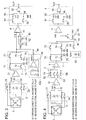
- Fig. 1 is a block diagram illustrating a magnetic sensor circuit according to an embodiment of the present invention.
- the magnetic sensor circuit includes a Hall element 1, a switch circuit 2, an amplifier 31, a switch circuit 7, a comparator 4, a switch circuit 41, voltage sources 42 and 43, a switch circuit 44, a voltage source 45, and a sample-and-hold circuit 9.
- the Hall element 1 is formed into a geometrically equivalent shape with respect to terminals A and A' and terminals B and B'.
- An effective signal component (hereinafter expressed by Voh) corresponding to a magnetic field strength, of a Hall voltage generated between the terminals (B'-B) when a voltage Vdd is applied between the terminals (A-A') of the Hall element 1 described above is equal in phase to that of a Hall voltage generated between the terminals (A-A') when the voltage Vdd is applied between the terminals (B-B').
- An offset voltage (hereinafter referred to as Vos) of the Hall element, of the Hall voltage generated between the terminals (B-B') is reversed in phase from that of the Hall voltage generated between the terminals (A-A').
- Vos of the Hall element 1 can be eliminated (offset cancelled) to determine only Voh.
- voltages determined by equally amplifying the two Hall voltages by a certain gain are averaged, a voltage determined by amplifying only Voh by a certain gain is determined.
- the switch circuit 2 includes switches 21, 22, 23, and 24 to connect the terminal A or the terminal B with a non-inverting input terminal (+) of the amplifier 31 through the switch circuit 2 and to connect the terminal A' or the terminal B' with an inverting input terminal (-) of the amplifier 31 therethrough.
- the amplifier 31 has a structure of a differential input and differential output type in which an operating point is set to output an arbitrary voltage, for example, Vdd/2, when the non-inverting input terminal (+) is equal in potential to the inverting input terminal (-).
- the non-inverting input terminal of the amplifier 31 is provided with a voltage source 32 based on the assumption of an offset voltage Vof2.
- Outputs of the amplifier 31 are input to the switch circuit 7 which includes switches 71, 72, 73, and 74 and capacitors 75 and 76 which are storage circuits and equal in capacitance value to each other.
- An output of the switch circuit 7 is connected with a non-inverting input terminal (+) of the comparator 4.
- the non-inverting input terminal (+) of the comparator 4 is also connected with the voltage source 45 generating a voltage Vprech through the switch circuit 44.
- An inverting input terminal (-) of the comparator 4 is connected with the voltage source 42 or 43 through the switch circuit 41.
- An output of the comparator 4 is connected with an output terminal OUT of the magnetic sensor circuit through the sample-and-hold circuit 9.
- the voltage Vdd from a voltage source (not shown) is applied between the terminals (A-A') during a first period, and the voltage Vdd therefrom is applied between the terminals (B-B') during a second period subsequent to the first period.
- the switch circuit 2 outputs the Hall voltage generated between the terminals (B-B') during the first period, and outputs the Hall voltage generated between the terminals (A-A') during the second period.
- the switch circuit 2 outputs, to the amplifier 31, the Hall voltage generated between the terminals (B-B') at a time when the voltage Vdd is applied between the terminals (A-A') during the first period, and outputs, to the amplifier 31, the Hall voltage generated between the terminals (A-A') at a time when the voltage Vdd is applied between the terminals (B-B') during the second period.
- the switch 71 is in an ON state and the switch 72 is in an OFF state.
- the switch 71 is in an OFF state and the switch 72 is in an ON state.
- the switch 73 and the switch 74 are in an OFF state. Therefore, the Hall voltages amplified by the amplifier 31 during the first period and the second period described above are stored as storage charge amounts corresponding to levels of the Hall voltages in the capacitors 75 and 76 which are the storage circuits, respectively. That is, during the first period, the Hall voltage for the first period is stored as the storage charge amount corresponding to the level of the Hall voltage in the capacitor 75 through the switch 71 which is in the ON state. During the second period, the Hall voltage for the second period is stored as the storage charge amount corresponding to the level of the Hall voltage in the capacitor 76 through the switch 72 which is in the ON state.
- the switches 71 and 72 are set to the OFF state and the switches 73 and 74 are set to an ON state. That is, the switch circuit 7 outputs, to the non-inverting input terminal (+) of the comparator 4, a voltage associated with the capacitors 75 and 76 connected in parallel with each other.
- the capacitors 75 and 76 are equal in capacitance value to each other, and hence this operation can be said to be an operation in which the switch circuit 7 outputs an average voltage of the Hall voltages for the first period and the second period described above, which are amplified by the amplifier 31.
- the voltage source 42 generating a threshold voltage Vth2 with respect to a forward magnetic flux or the voltage source 43 generating a threshold voltage Vth3 with respect to a reverse magnetic flux is connected with the inverting input terminal (-) of the comparator 4 through the switch circuit 41.
- the comparator 4 compares the voltage output from the switch circuit 7 with the threshold voltage Vth2 or the threshold voltage Vth3.
- the sample-and-hold circuit 9 includes a first sample-and-hold circuit including a switch 91 and a capacitor 93, a second sample-and-hold circuit including a switch 92 and a capacitor 94, and a logic circuit 95.
- the switches 91 and 92 are operated in conjunction with the switch circuit 41.
- a result obtained by detecting the forward magnetic flux is stored in the capacitor 93.
- a result obtained by detecting the reverse magnetic flux is stored in the capacitor 94.
- the high level is output to the output terminal OUT.
- ground capacitor "cinp" associated with the non-inverting input terminal (+) of the comparator 4 is taken into account, during the third period described above, the ground capacitor "cinp” can be said to be connected in parallel with the capacitors 75 and 76.
- Vcinpc C ⁇ ⁇ Vc ⁇ 75 ⁇ b + C ⁇ ⁇ Vc ⁇ 76 ⁇ b + cinp ⁇ Vcinpb / 2 ⁇ C ⁇ + cinp
- the voltage Vc75b associated with the capacitor 75 immediately before the completion of the second period is, that is, equal to a voltage value which is generated during the first period and associated with the capacitor 75. This voltage is determined as follows. A value determined by multiplying a voltage (-Voh-Vos-Vof2) by a gain (hereinafter expressed by A31) of the amplifier 31 is divided into two and then subtracted from Vdd/2 to determine the voltage Vc75b.
- Vc ⁇ 75 ⁇ b Vdd / 2 + - Voh - Vos - Vof ⁇ 2 ⁇ A ⁇ 31 / 2
- the voltage Vc76b associated with the capacitor 76 immediately before the completion of the second period is, that is, equal to a voltage value which is generated during the second period and associated with the capacitor 76.
- This voltage is determined as follows. A value determined by multiplying a voltage (+Voh-Vos-Vof2) by A31 of the amplifier 31 is divided into two and then added to Vdd/2 to determine the voltage Vc76b.
- Vcinpc Vdd / 2 + Voh ⁇ A ⁇ 31 / 2 ⁇ 2 ⁇ C ⁇ + cinp ⁇ Vcinpb / 2 ⁇ C ⁇ + cinp
- Expression (4) is changed as follows.
- Vcinpc Vdd / 2 + cinp / 2 ⁇ C ⁇ + cinp ⁇ ⁇ + Voh ⁇ A ⁇ 31 ⁇ C ⁇ / 2 ⁇ C ⁇ + cinp
- the comparator 4 performs comparison operation based on the assumption that a state in which the voltage input to the non-inverting input terminal (+) thereof is Vdd/2 is a state in which the magnetic flux passing through the Hall element 1 is zero. In a case where ⁇ is not zero in Expression (5), when the effective signal component Voh corresponding to the magnetic field strength is zero, Vcinpc is not equal to Vdd/2, whereby an offset occurs in the comparator 4, which is not preferable.
- the voltage source 45 and the switch circuit 44 are provided to have a function for supplying, as Vcinpb, a voltage Vprech, that is, Vdd/2 to the non-inverting input terminal (+) of the comparator 4.
- the switch circuit 44 is in an ON state, whereby the voltage Vprech, that is, Vdd/2 from the voltage source 45 is connected with the non-inverting input terminal (+) of the comparator 4.
- the ground capacitor "cinp" of the non-inverting input terminal (+) of the comparator 4 is charged to the voltage Vprech, that is, Vdd/2 supplied from the voltage source 45.
- the switch circuit 44 is turned off at a time immediately before the completion of the second period. Therefore, the offset can be prevented from occurring in the comparator 4.
- the voltage source 45 may have a structure in which a power source voltage is output through resistance division, as in a voltage source 45a illustrated in Fig. 2 or may have a structure in which a voltage follower circuit 46 is provided to receive an output determined by resistance division of the power source voltage, as in a voltage source 45b illustrated in Fig. 3 .
- the magnetic sensor circuit in the embodiment of the present invention it is possible to eliminate (offset-cancel) both the offset of the Hall element itself and the offset of the circuit provided in the subsequent stage. Therefore, a high-performance magnetic sensor circuit can be provided.
- the switch circuit 7 includes the switches 71, 72, 73, and 74 and the capacitors 75 and 76.
- the present invention is not limited to such a circuit structure described above.
- the operating point of the amplifier 31 is set such that the output voltage thereof is Vdd/2 when no signal is input, that is, when the non-inverting input terminal (+) thereof is equal in potential to the inverting input terminal (-) thereof.
- ⁇ another voltage value (hereinafter expressed by ⁇ ) other than Vdd/2, when the voltage Vprech supplied from the voltage source 45 is set to ⁇ , the same effect is obviously obtained.
- the amplifier includes only the amplifier 31 of the differential input and differential output type.
- the outputs of the amplifier 31 may be connected with an amplifier 6 having a gain A6 through a switch circuit 5.
- switches 51 and 54 are set to an ON state and switches 52 and 53 are set to an OFF state.
- the switches 51 and 54 are set to an OFF state and the switches 52 and 53 are set to an ON state.
- Vcinpc can be expressed as follows by rewriting (A31/2) into (A31 ⁇ A6) in Expression (6).
- Vcinpc Vdd / 2 + Voh ⁇ 2 ⁇ A ⁇ 31 ⁇ A ⁇ 6 ⁇ C ⁇ / 2 ⁇ C ⁇ + cinp Therefore, the same effect is obviously obtained.
- Another circuit structure for providing the same function may be used.
- the sample-and-hold circuit 9 has been described as the circuit located in the subsequent stage of the comparator 4.
- the present invention is not limited to such a circuit structure described above.
- the magnetic sensor circuit dealing with the forward and reverse magnetic fluxes.
- the magnetic sensor circuit is sufficient to deal with only any one of the magnetic fluxes, it is apparent that only one of the voltage sources 42 and 43 is provided.
- Fig. 5 illustrates an embodiment in which a buffer circuit 8 is provided as the circuit for monitoring the magnetic field in the subsequent stage of the switch circuit 7.
- the buffer circuit 8 samples the voltage Vcinpc and outputs, to the output terminal OUT, the sampled voltage as a voltage signal indicating a magnetic flux strength.
- the buffer circuit 8 includes a voltage follower circuit 81, a switch 82, and a capacitor 83.
- the magnetic sensor circuit of the present invention it is possible to eliminate (offset-cancel) both the offset of the Hall element itself and the offset of the circuit provided in the subsequent stage. Therefore, a high-performance magnetic sensor circuit can be provided.
- the magnetic sensor circuit including the Hall element can be used to detect a state of a folding mechanism. Therefore, the present invention can also be applied to the use of a portable communication device having the folding mechanism, such as a cellular phone.
Landscapes
- Physics & Mathematics (AREA)
- Condensed Matter Physics & Semiconductors (AREA)
- General Physics & Mathematics (AREA)
- Measuring Magnetic Variables (AREA)
- Hall/Mr Elements (AREA)
- Geophysics And Detection Of Objects (AREA)
- Investigating Or Analyzing Materials By The Use Of Magnetic Means (AREA)
Applications Claiming Priority (2)
| Application Number | Priority Date | Filing Date | Title |
|---|---|---|---|
| JP2007193084A JP5052982B2 (ja) | 2007-07-25 | 2007-07-25 | 磁気センサ回路 |
| PCT/JP2008/062522 WO2009014013A1 (ja) | 2007-07-25 | 2008-07-10 | 磁気センサ回路 |
Publications (3)
| Publication Number | Publication Date |
|---|---|
| EP2101184A1 EP2101184A1 (en) | 2009-09-16 |
| EP2101184A4 EP2101184A4 (en) | 2010-09-15 |
| EP2101184B1 true EP2101184B1 (en) | 2011-10-05 |
Family
ID=40281271
Family Applications (1)
| Application Number | Title | Priority Date | Filing Date |
|---|---|---|---|
| EP08791070A Not-in-force EP2101184B1 (en) | 2007-07-25 | 2008-07-10 | Magnetic sensor circuit |
Country Status (8)
| Country | Link |
|---|---|
| US (1) | US8274281B2 (enExample) |
| EP (1) | EP2101184B1 (enExample) |
| JP (1) | JP5052982B2 (enExample) |
| KR (1) | KR101118457B1 (enExample) |
| CN (1) | CN101802632B (enExample) |
| AT (1) | ATE527551T1 (enExample) |
| TW (1) | TWI427311B (enExample) |
| WO (1) | WO2009014013A1 (enExample) |
Families Citing this family (13)
| Publication number | Priority date | Publication date | Assignee | Title |
|---|---|---|---|---|
| KR101406772B1 (ko) | 2007-10-22 | 2014-06-19 | 다우 글로벌 테크놀로지스 엘엘씨 | 중합체 조성물 및 제품의 성형방법 |
| JP2010281764A (ja) * | 2009-06-08 | 2010-12-16 | Sanyo Electric Co Ltd | オフセットキャンセル回路 |
| JP2011075338A (ja) | 2009-09-29 | 2011-04-14 | Seiko Instruments Inc | 磁気センサ回路 |
| JP5411818B2 (ja) * | 2010-08-26 | 2014-02-12 | セミコンダクター・コンポーネンツ・インダストリーズ・リミテッド・ライアビリティ・カンパニー | 半導体装置 |
| TWI439046B (zh) | 2011-08-12 | 2014-05-21 | Richtek Technology Corp | 自動調零放大器及相關的偵測模組 |
| JP5926081B2 (ja) * | 2012-03-22 | 2016-05-25 | エスアイアイ・セミコンダクタ株式会社 | センサ装置 |
| US9638548B2 (en) | 2012-05-07 | 2017-05-02 | Infineon Technologies Ag | Output switching systems and methods for magnetic field sensors |
| EP2848957B1 (en) | 2012-05-11 | 2017-03-29 | Asahi Kasei Microdevices Corporation | Magnetism detection device and magnetism detection method |
| JP6004758B2 (ja) * | 2012-06-07 | 2016-10-12 | エスアイアイ・セミコンダクタ株式会社 | 磁気センサ |
| CN102854535B (zh) * | 2012-08-24 | 2015-03-11 | 中国船舶重工集团公司第七二二研究所 | 一种宽带磁性传感器 |
| JP6503198B2 (ja) * | 2015-03-05 | 2019-04-17 | エイブリック株式会社 | 比較回路およびセンサ装置 |
| JP2018054473A (ja) * | 2016-09-29 | 2018-04-05 | アイシン精機株式会社 | 磁気センサ及び磁気センサシステム |
| US11016151B2 (en) * | 2018-03-14 | 2021-05-25 | Ablic Inc. | Semiconductor device and method of adjusting the same |
Family Cites Families (7)
| Publication number | Priority date | Publication date | Assignee | Title |
|---|---|---|---|---|
| JP2776783B2 (ja) | 1995-12-19 | 1998-07-16 | 埼玉日本電気株式会社 | 移動状態検出回路 |
| US6777932B2 (en) * | 2000-03-23 | 2004-08-17 | Matsushita Electric Industrial Co., Ltd. | Magnetic field sensor |
| JP4451577B2 (ja) * | 2001-07-26 | 2010-04-14 | パナソニック株式会社 | 磁界センサ |
| JP3887275B2 (ja) * | 2002-07-03 | 2007-02-28 | 東光株式会社 | センサ回路 |
| JP4049757B2 (ja) * | 2004-03-12 | 2008-02-20 | 東光株式会社 | 磁気センサ回路 |
| JP4303631B2 (ja) * | 2004-04-09 | 2009-07-29 | 東光株式会社 | センサ回路 |
| JP4901720B2 (ja) * | 2005-02-08 | 2012-03-21 | ローム株式会社 | 磁気センサ回路、及び、その磁気センサ回路を有する携帯端末 |
-
2007
- 2007-07-25 JP JP2007193084A patent/JP5052982B2/ja not_active Expired - Fee Related
-
2008
- 2008-07-10 KR KR1020097014905A patent/KR101118457B1/ko not_active Expired - Fee Related
- 2008-07-10 EP EP08791070A patent/EP2101184B1/en not_active Not-in-force
- 2008-07-10 WO PCT/JP2008/062522 patent/WO2009014013A1/ja not_active Ceased
- 2008-07-10 US US12/594,894 patent/US8274281B2/en not_active Expired - Fee Related
- 2008-07-10 CN CN2008801005999A patent/CN101802632B/zh not_active Expired - Fee Related
- 2008-07-10 AT AT08791070T patent/ATE527551T1/de not_active IP Right Cessation
- 2008-07-14 TW TW097126654A patent/TWI427311B/zh not_active IP Right Cessation
Also Published As
| Publication number | Publication date |
|---|---|
| US20100117640A1 (en) | 2010-05-13 |
| TWI427311B (zh) | 2014-02-21 |
| CN101802632B (zh) | 2013-04-24 |
| ATE527551T1 (de) | 2011-10-15 |
| JP2009031027A (ja) | 2009-02-12 |
| EP2101184A1 (en) | 2009-09-16 |
| CN101802632A (zh) | 2010-08-11 |
| US8274281B2 (en) | 2012-09-25 |
| JP5052982B2 (ja) | 2012-10-17 |
| EP2101184A4 (en) | 2010-09-15 |
| KR101118457B1 (ko) | 2012-03-06 |
| TW200925629A (en) | 2009-06-16 |
| KR20100039269A (ko) | 2010-04-15 |
| WO2009014013A1 (ja) | 2009-01-29 |
Similar Documents
| Publication | Publication Date | Title |
|---|---|---|
| EP2101184B1 (en) | Magnetic sensor circuit | |
| CN101907691B (zh) | 磁性传感器装置 | |
| JP4241787B2 (ja) | 組電池総電圧検出およびリーク検出装置 | |
| US7459887B2 (en) | Voltage detection circuit, overcurrent detection circuit, charging current control system, and voltage detection method | |
| EP2829889B1 (en) | Sensor device | |
| US20090009163A1 (en) | Magnetic sensing device and electronic compass using the same | |
| TWI640794B (zh) | 感測器裝置 | |
| US20130076350A1 (en) | Magnetic sensor device | |
| CN108572338B (zh) | 磁传感器电路 | |
| CN104254784A (zh) | 传感器装置 | |
| US7994771B2 (en) | Current measurement circuit, current detection circuit and saturation prevention and recovery circuit for operational amplifier | |
| US7023352B2 (en) | Voltage-detecting method and related circuits | |
| EP2860541B1 (en) | Magnetic sensor | |
| EP3564686A1 (en) | Zero cross detection circuit and sensor device | |
| JP4049757B2 (ja) | 磁気センサ回路 | |
| US9837997B2 (en) | Comparison circuit and sensor device | |
| EP3561526A1 (en) | Zero cross detection circuit and sensor device | |
| JP6110639B2 (ja) | センサ閾値決定回路 | |
| CN104569563A (zh) | 一种高速串行数据的包络检测器 | |
| CN112114257A (zh) | 电压电流转换电路及充放电控制装置 | |
| JP4064303B2 (ja) | センスコンパレータ回路とそのオフセット補償方法 | |
| CN102957385B (zh) | 自动调零放大器及相关的检测模块 | |
| WO2014125846A1 (ja) | 磁気センサ |
Legal Events
| Date | Code | Title | Description |
|---|---|---|---|
| PUAI | Public reference made under article 153(3) epc to a published international application that has entered the european phase |
Free format text: ORIGINAL CODE: 0009012 |
|
| 17P | Request for examination filed |
Effective date: 20090701 |
|
| AK | Designated contracting states |
Kind code of ref document: A1 Designated state(s): AT BE BG CH CY CZ DE DK EE ES FI FR GB GR HR HU IE IS IT LI LT LU LV MC MT NL NO PL PT RO SE SI SK TR |
|
| A4 | Supplementary search report drawn up and despatched |
Effective date: 20100818 |
|
| DAX | Request for extension of the european patent (deleted) | ||
| GRAP | Despatch of communication of intention to grant a patent |
Free format text: ORIGINAL CODE: EPIDOSNIGR1 |
|
| RIC1 | Information provided on ipc code assigned before grant |
Ipc: G01R 33/07 20060101AFI20110331BHEP |
|
| GRAS | Grant fee paid |
Free format text: ORIGINAL CODE: EPIDOSNIGR3 |
|
| GRAA | (expected) grant |
Free format text: ORIGINAL CODE: 0009210 |
|
| AK | Designated contracting states |
Kind code of ref document: B1 Designated state(s): AT BE BG CH CY CZ DE DK EE ES FI FR GB GR HR HU IE IS IT LI LT LU LV MC MT NL NO PL PT RO SE SI SK TR |
|
| REG | Reference to a national code |
Ref country code: GB Ref legal event code: FG4D |
|
| REG | Reference to a national code |
Ref country code: CH Ref legal event code: EP |
|
| REG | Reference to a national code |
Ref country code: IE Ref legal event code: FG4D |
|
| REG | Reference to a national code |
Ref country code: DE Ref legal event code: R096 Ref document number: 602008010277 Country of ref document: DE Effective date: 20111208 |
|
| REG | Reference to a national code |
Ref country code: NL Ref legal event code: VDEP Effective date: 20111005 |
|
| PG25 | Lapsed in a contracting state [announced via postgrant information from national office to epo] |
Ref country code: SI Free format text: LAPSE BECAUSE OF FAILURE TO SUBMIT A TRANSLATION OF THE DESCRIPTION OR TO PAY THE FEE WITHIN THE PRESCRIBED TIME-LIMIT Effective date: 20111005 |
|
| LTIE | Lt: invalidation of european patent or patent extension |
Effective date: 20111005 |
|
| REG | Reference to a national code |
Ref country code: AT Ref legal event code: MK05 Ref document number: 527551 Country of ref document: AT Kind code of ref document: T Effective date: 20111005 |
|
| PG25 | Lapsed in a contracting state [announced via postgrant information from national office to epo] |
Ref country code: IS Free format text: LAPSE BECAUSE OF FAILURE TO SUBMIT A TRANSLATION OF THE DESCRIPTION OR TO PAY THE FEE WITHIN THE PRESCRIBED TIME-LIMIT Effective date: 20120205 Ref country code: LT Free format text: LAPSE BECAUSE OF FAILURE TO SUBMIT A TRANSLATION OF THE DESCRIPTION OR TO PAY THE FEE WITHIN THE PRESCRIBED TIME-LIMIT Effective date: 20111005 Ref country code: NO Free format text: LAPSE BECAUSE OF FAILURE TO SUBMIT A TRANSLATION OF THE DESCRIPTION OR TO PAY THE FEE WITHIN THE PRESCRIBED TIME-LIMIT Effective date: 20120105 Ref country code: BE Free format text: LAPSE BECAUSE OF FAILURE TO SUBMIT A TRANSLATION OF THE DESCRIPTION OR TO PAY THE FEE WITHIN THE PRESCRIBED TIME-LIMIT Effective date: 20111005 |
|
| PG25 | Lapsed in a contracting state [announced via postgrant information from national office to epo] |
Ref country code: SE Free format text: LAPSE BECAUSE OF FAILURE TO SUBMIT A TRANSLATION OF THE DESCRIPTION OR TO PAY THE FEE WITHIN THE PRESCRIBED TIME-LIMIT Effective date: 20111005 Ref country code: PT Free format text: LAPSE BECAUSE OF FAILURE TO SUBMIT A TRANSLATION OF THE DESCRIPTION OR TO PAY THE FEE WITHIN THE PRESCRIBED TIME-LIMIT Effective date: 20120206 Ref country code: LV Free format text: LAPSE BECAUSE OF FAILURE TO SUBMIT A TRANSLATION OF THE DESCRIPTION OR TO PAY THE FEE WITHIN THE PRESCRIBED TIME-LIMIT Effective date: 20111005 Ref country code: HR Free format text: LAPSE BECAUSE OF FAILURE TO SUBMIT A TRANSLATION OF THE DESCRIPTION OR TO PAY THE FEE WITHIN THE PRESCRIBED TIME-LIMIT Effective date: 20111005 Ref country code: NL Free format text: LAPSE BECAUSE OF FAILURE TO SUBMIT A TRANSLATION OF THE DESCRIPTION OR TO PAY THE FEE WITHIN THE PRESCRIBED TIME-LIMIT Effective date: 20111005 Ref country code: GR Free format text: LAPSE BECAUSE OF FAILURE TO SUBMIT A TRANSLATION OF THE DESCRIPTION OR TO PAY THE FEE WITHIN THE PRESCRIBED TIME-LIMIT Effective date: 20120106 |
|
| PG25 | Lapsed in a contracting state [announced via postgrant information from national office to epo] |
Ref country code: CY Free format text: LAPSE BECAUSE OF FAILURE TO SUBMIT A TRANSLATION OF THE DESCRIPTION OR TO PAY THE FEE WITHIN THE PRESCRIBED TIME-LIMIT Effective date: 20111005 |
|
| PG25 | Lapsed in a contracting state [announced via postgrant information from national office to epo] |
Ref country code: BG Free format text: LAPSE BECAUSE OF FAILURE TO SUBMIT A TRANSLATION OF THE DESCRIPTION OR TO PAY THE FEE WITHIN THE PRESCRIBED TIME-LIMIT Effective date: 20120105 Ref country code: EE Free format text: LAPSE BECAUSE OF FAILURE TO SUBMIT A TRANSLATION OF THE DESCRIPTION OR TO PAY THE FEE WITHIN THE PRESCRIBED TIME-LIMIT Effective date: 20111005 Ref country code: DK Free format text: LAPSE BECAUSE OF FAILURE TO SUBMIT A TRANSLATION OF THE DESCRIPTION OR TO PAY THE FEE WITHIN THE PRESCRIBED TIME-LIMIT Effective date: 20111005 Ref country code: SK Free format text: LAPSE BECAUSE OF FAILURE TO SUBMIT A TRANSLATION OF THE DESCRIPTION OR TO PAY THE FEE WITHIN THE PRESCRIBED TIME-LIMIT Effective date: 20111005 Ref country code: CZ Free format text: LAPSE BECAUSE OF FAILURE TO SUBMIT A TRANSLATION OF THE DESCRIPTION OR TO PAY THE FEE WITHIN THE PRESCRIBED TIME-LIMIT Effective date: 20111005 |
|
| PLBE | No opposition filed within time limit |
Free format text: ORIGINAL CODE: 0009261 |
|
| STAA | Information on the status of an ep patent application or granted ep patent |
Free format text: STATUS: NO OPPOSITION FILED WITHIN TIME LIMIT |
|
| PG25 | Lapsed in a contracting state [announced via postgrant information from national office to epo] |
Ref country code: PL Free format text: LAPSE BECAUSE OF FAILURE TO SUBMIT A TRANSLATION OF THE DESCRIPTION OR TO PAY THE FEE WITHIN THE PRESCRIBED TIME-LIMIT Effective date: 20111005 Ref country code: RO Free format text: LAPSE BECAUSE OF FAILURE TO SUBMIT A TRANSLATION OF THE DESCRIPTION OR TO PAY THE FEE WITHIN THE PRESCRIBED TIME-LIMIT Effective date: 20111005 Ref country code: IT Free format text: LAPSE BECAUSE OF FAILURE TO SUBMIT A TRANSLATION OF THE DESCRIPTION OR TO PAY THE FEE WITHIN THE PRESCRIBED TIME-LIMIT Effective date: 20111005 |
|
| 26N | No opposition filed |
Effective date: 20120706 |
|
| REG | Reference to a national code |
Ref country code: DE Ref legal event code: R097 Ref document number: 602008010277 Country of ref document: DE Effective date: 20120706 |
|
| PG25 | Lapsed in a contracting state [announced via postgrant information from national office to epo] |
Ref country code: AT Free format text: LAPSE BECAUSE OF FAILURE TO SUBMIT A TRANSLATION OF THE DESCRIPTION OR TO PAY THE FEE WITHIN THE PRESCRIBED TIME-LIMIT Effective date: 20111005 |
|
| PG25 | Lapsed in a contracting state [announced via postgrant information from national office to epo] |
Ref country code: MC Free format text: LAPSE BECAUSE OF NON-PAYMENT OF DUE FEES Effective date: 20120731 |
|
| REG | Reference to a national code |
Ref country code: CH Ref legal event code: PL |
|
| GBPC | Gb: european patent ceased through non-payment of renewal fee |
Effective date: 20120710 |
|
| REG | Reference to a national code |
Ref country code: FR Ref legal event code: ST Effective date: 20130329 |
|
| PG25 | Lapsed in a contracting state [announced via postgrant information from national office to epo] |
Ref country code: LI Free format text: LAPSE BECAUSE OF NON-PAYMENT OF DUE FEES Effective date: 20120731 Ref country code: ES Free format text: LAPSE BECAUSE OF FAILURE TO SUBMIT A TRANSLATION OF THE DESCRIPTION OR TO PAY THE FEE WITHIN THE PRESCRIBED TIME-LIMIT Effective date: 20120116 Ref country code: GB Free format text: LAPSE BECAUSE OF NON-PAYMENT OF DUE FEES Effective date: 20120710 Ref country code: CH Free format text: LAPSE BECAUSE OF NON-PAYMENT OF DUE FEES Effective date: 20120731 Ref country code: FR Free format text: LAPSE BECAUSE OF NON-PAYMENT OF DUE FEES Effective date: 20120731 |
|
| REG | Reference to a national code |
Ref country code: IE Ref legal event code: MM4A |
|
| PG25 | Lapsed in a contracting state [announced via postgrant information from national office to epo] |
Ref country code: FI Free format text: LAPSE BECAUSE OF FAILURE TO SUBMIT A TRANSLATION OF THE DESCRIPTION OR TO PAY THE FEE WITHIN THE PRESCRIBED TIME-LIMIT Effective date: 20111005 |
|
| PG25 | Lapsed in a contracting state [announced via postgrant information from national office to epo] |
Ref country code: MT Free format text: LAPSE BECAUSE OF FAILURE TO SUBMIT A TRANSLATION OF THE DESCRIPTION OR TO PAY THE FEE WITHIN THE PRESCRIBED TIME-LIMIT Effective date: 20111005 Ref country code: IE Free format text: LAPSE BECAUSE OF NON-PAYMENT OF DUE FEES Effective date: 20120710 |
|
| PG25 | Lapsed in a contracting state [announced via postgrant information from national office to epo] |
Ref country code: TR Free format text: LAPSE BECAUSE OF FAILURE TO SUBMIT A TRANSLATION OF THE DESCRIPTION OR TO PAY THE FEE WITHIN THE PRESCRIBED TIME-LIMIT Effective date: 20111005 |
|
| PG25 | Lapsed in a contracting state [announced via postgrant information from national office to epo] |
Ref country code: LU Free format text: LAPSE BECAUSE OF NON-PAYMENT OF DUE FEES Effective date: 20120710 |
|
| PG25 | Lapsed in a contracting state [announced via postgrant information from national office to epo] |
Ref country code: HU Free format text: LAPSE BECAUSE OF FAILURE TO SUBMIT A TRANSLATION OF THE DESCRIPTION OR TO PAY THE FEE WITHIN THE PRESCRIBED TIME-LIMIT Effective date: 20080710 |
|
| REG | Reference to a national code |
Ref country code: DE Ref legal event code: R081 Ref document number: 602008010277 Country of ref document: DE Owner name: SII SEMICONDUCTOR CORPORATION, CHIBA-SHI, JP Free format text: FORMER OWNER: SEIKO INSTRUMENTS INC., CHIBA, JP Ref country code: DE Ref legal event code: R081 Ref document number: 602008010277 Country of ref document: DE Owner name: ABLIC INC., JP Free format text: FORMER OWNER: SEIKO INSTRUMENTS INC., CHIBA, JP |
|
| REG | Reference to a national code |
Ref country code: DE Ref legal event code: R081 Ref document number: 602008010277 Country of ref document: DE Owner name: ABLIC INC., JP Free format text: FORMER OWNER: SII SEMICONDUCTOR CORPORATION, CHIBA-SHI, CHIBA-KEN, JP |
|
| PGFP | Annual fee paid to national office [announced via postgrant information from national office to epo] |
Ref country code: DE Payment date: 20190625 Year of fee payment: 12 |
|
| REG | Reference to a national code |
Ref country code: DE Ref legal event code: R119 Ref document number: 602008010277 Country of ref document: DE |
|
| PG25 | Lapsed in a contracting state [announced via postgrant information from national office to epo] |
Ref country code: DE Free format text: LAPSE BECAUSE OF NON-PAYMENT OF DUE FEES Effective date: 20210202 |