EP2048922A2 - COF-Platte - Google Patents
COF-Platte Download PDFInfo
- Publication number
- EP2048922A2 EP2048922A2 EP08162744A EP08162744A EP2048922A2 EP 2048922 A2 EP2048922 A2 EP 2048922A2 EP 08162744 A EP08162744 A EP 08162744A EP 08162744 A EP08162744 A EP 08162744A EP 2048922 A2 EP2048922 A2 EP 2048922A2
- Authority
- EP
- European Patent Office
- Prior art keywords
- leads
- lead
- longitudinal direction
- dummy
- portions
- Prior art date
- Legal status (The legal status is an assumption and is not a legal conclusion. Google has not performed a legal analysis and makes no representation as to the accuracy of the status listed.)
- Withdrawn
Links
Images


Classifications
-
- H—ELECTRICITY
- H05—ELECTRIC TECHNIQUES NOT OTHERWISE PROVIDED FOR
- H05K—PRINTED CIRCUITS; CASINGS OR CONSTRUCTIONAL DETAILS OF ELECTRIC APPARATUS; MANUFACTURE OF ASSEMBLAGES OF ELECTRICAL COMPONENTS
- H05K1/00—Printed circuits
- H05K1/02—Details
- H05K1/11—Printed elements for providing electric connections to or between printed circuits
- H05K1/111—Pads for surface mounting, e.g. lay-out
-
- H—ELECTRICITY
- H10—SEMICONDUCTOR DEVICES; ELECTRIC SOLID-STATE DEVICES NOT OTHERWISE PROVIDED FOR
- H10W—GENERIC PACKAGES, INTERCONNECTIONS, CONNECTORS OR OTHER CONSTRUCTIONAL DETAILS OF DEVICES COVERED BY CLASS H10
- H10W70/00—Package substrates; Interposers; Redistribution layers [RDL]
- H10W70/60—Insulating or insulated package substrates; Interposers; Redistribution layers
- H10W70/62—Insulating or insulated package substrates; Interposers; Redistribution layers characterised by their interconnections
- H10W70/65—Shapes or dispositions of interconnections
-
- H—ELECTRICITY
- H10—SEMICONDUCTOR DEVICES; ELECTRIC SOLID-STATE DEVICES NOT OTHERWISE PROVIDED FOR
- H10W—GENERIC PACKAGES, INTERCONNECTIONS, CONNECTORS OR OTHER CONSTRUCTIONAL DETAILS OF DEVICES COVERED BY CLASS H10
- H10W70/00—Package substrates; Interposers; Redistribution layers [RDL]
- H10W70/60—Insulating or insulated package substrates; Interposers; Redistribution layers
- H10W70/67—Insulating or insulated package substrates; Interposers; Redistribution layers characterised by their insulating layers or insulating parts
- H10W70/688—Flexible insulating substrates
-
- H—ELECTRICITY
- H05—ELECTRIC TECHNIQUES NOT OTHERWISE PROVIDED FOR
- H05K—PRINTED CIRCUITS; CASINGS OR CONSTRUCTIONAL DETAILS OF ELECTRIC APPARATUS; MANUFACTURE OF ASSEMBLAGES OF ELECTRICAL COMPONENTS
- H05K1/00—Printed circuits
- H05K1/02—Details
- H05K1/03—Use of materials for the substrate
- H05K1/05—Insulated conductive substrates, e.g. insulated metal substrate
- H05K1/056—Insulated conductive substrates, e.g. insulated metal substrate the metal substrate being covered by an organic insulating layer
-
- H—ELECTRICITY
- H05—ELECTRIC TECHNIQUES NOT OTHERWISE PROVIDED FOR
- H05K—PRINTED CIRCUITS; CASINGS OR CONSTRUCTIONAL DETAILS OF ELECTRIC APPARATUS; MANUFACTURE OF ASSEMBLAGES OF ELECTRICAL COMPONENTS
- H05K1/00—Printed circuits
- H05K1/18—Printed circuits structurally associated with non-printed electric components
- H05K1/189—Printed circuits structurally associated with non-printed electric components characterised by the use of flexible or folded printed circuits
-
- H—ELECTRICITY
- H05—ELECTRIC TECHNIQUES NOT OTHERWISE PROVIDED FOR
- H05K—PRINTED CIRCUITS; CASINGS OR CONSTRUCTIONAL DETAILS OF ELECTRIC APPARATUS; MANUFACTURE OF ASSEMBLAGES OF ELECTRICAL COMPONENTS
- H05K2201/00—Indexing scheme relating to printed circuits covered by H05K1/00
- H05K2201/09—Shape and layout
- H05K2201/09209—Shape and layout details of conductors
- H05K2201/09654—Shape and layout details of conductors covering at least two types of conductors provided for in H05K2201/09218 - H05K2201/095
- H05K2201/09709—Staggered pads, lands or terminals; Parallel conductors in different planes
-
- H—ELECTRICITY
- H05—ELECTRIC TECHNIQUES NOT OTHERWISE PROVIDED FOR
- H05K—PRINTED CIRCUITS; CASINGS OR CONSTRUCTIONAL DETAILS OF ELECTRIC APPARATUS; MANUFACTURE OF ASSEMBLAGES OF ELECTRICAL COMPONENTS
- H05K2201/00—Indexing scheme relating to printed circuits covered by H05K1/00
- H05K2201/09—Shape and layout
- H05K2201/09209—Shape and layout details of conductors
- H05K2201/09654—Shape and layout details of conductors covering at least two types of conductors provided for in H05K2201/09218 - H05K2201/095
- H05K2201/09781—Dummy conductors, i.e. not used for normal transport of current; Dummy electrodes of components
-
- H—ELECTRICITY
- H05—ELECTRIC TECHNIQUES NOT OTHERWISE PROVIDED FOR
- H05K—PRINTED CIRCUITS; CASINGS OR CONSTRUCTIONAL DETAILS OF ELECTRIC APPARATUS; MANUFACTURE OF ASSEMBLAGES OF ELECTRICAL COMPONENTS
- H05K2201/00—Indexing scheme relating to printed circuits covered by H05K1/00
- H05K2201/10—Details of components or other objects attached to or integrated in a printed circuit board
- H05K2201/10613—Details of electrical connections of non-printed components, e.g. special leads
- H05K2201/10621—Components characterised by their electrical contacts
- H05K2201/10674—Flip chip
-
- H—ELECTRICITY
- H05—ELECTRIC TECHNIQUES NOT OTHERWISE PROVIDED FOR
- H05K—PRINTED CIRCUITS; CASINGS OR CONSTRUCTIONAL DETAILS OF ELECTRIC APPARATUS; MANUFACTURE OF ASSEMBLAGES OF ELECTRICAL COMPONENTS
- H05K2203/00—Indexing scheme relating to apparatus or processes for manufacturing printed circuits covered by H05K3/00
- H05K2203/15—Position of the PCB during processing
- H05K2203/1545—Continuous processing, i.e. involving rolls moving a band-like or solid carrier along a continuous production path
-
- Y—GENERAL TAGGING OF NEW TECHNOLOGICAL DEVELOPMENTS; GENERAL TAGGING OF CROSS-SECTIONAL TECHNOLOGIES SPANNING OVER SEVERAL SECTIONS OF THE IPC; TECHNICAL SUBJECTS COVERED BY FORMER USPC CROSS-REFERENCE ART COLLECTIONS [XRACs] AND DIGESTS
- Y02—TECHNOLOGIES OR APPLICATIONS FOR MITIGATION OR ADAPTATION AGAINST CLIMATE CHANGE
- Y02P—CLIMATE CHANGE MITIGATION TECHNOLOGIES IN THE PRODUCTION OR PROCESSING OF GOODS
- Y02P70/00—Climate change mitigation technologies in the production process for final industrial or consumer products
- Y02P70/50—Manufacturing or production processes characterised by the final manufactured product
Definitions
- the present invention relates to a COF board and, more particularly, to a COF board for mounting an electronic component.
- COF board On a COF board, an electronic component such as a semiconductor element (an IC chip and the like) is nakedly mounted (bare-chip mounted) without being contained in a package by a COF (Chip on film) method.
- the COF board is mounted on various electronic equipment.
- the COF board typically includes an insulating base layer, and terminal portions formed thereon to be connected to the connection terminals of the electronic component.
- terminal portions each including a shorter lead and a longer lead are formed at the end portions of belt-like conductors of a wired circuit board (see, e.g., Japanese Unexamined Patent No. 2005-183465 ).
- a plurality of the shorter leads extend in a direction in which the belt-like conductors extend, and are arranged in spaced-apart relation in a direction perpendicular to the extending direction thereof (widthwise direction).
- a plurality of the longer leads are arranged between the mutually adjacent shorter leads in spaced-apart relation in the widthwise direction.
- the terminal portions proposed in Japanese Unexamined Patent No. 2005-183465 are formed in an alternating and staggered arrangement (a two-row checker pattern), wherein the end portions of the shorter leads, and the end portions of the longer leads along the widthwise direction.
- the terminal portions of the COF board may be formed by electrolytic plating in an additive method or the like by precipitating a metal in a plating solution in which the COF board is dipped.
- the pattern density with respect to the plating solution at a longer terminal end portions is lower than that at a shorter terminal end portions and the longer leads except for the longer terminal end portions. That is, density unevenness of the leads with respect to the plating solution are caused, so that the concentration of metal ions in the plating solution is higher in the vicinities of the longer terminal end portions than in the vicinities of the shorter terminal end portions. Accordingly, the metal is precipitated in a larger amount at the longer terminal end portions than at the shorter terminal end portions, so that the longer terminal end portions are thicker than the shorter terminal end portions.
- a gap is easily caused between the thinner shorter terminal end portions and the connection terminal of the semiconductor element. This leads to defective connection to cause degradation of connection reliability.
- a COF board of the present invention includes an insulating layer, and a terminal portion formed on the insulating layer, and electrically connected to an electronic component, wherein the terminal portion includes a first lead extending in a longitudinal direction, and a second lead extending in the longitudinal direction, and having a length in the longitudinal direction smaller than a length of the first lead in the longitudinal direction, a plurality of the first leads are arranged in spaced-apart relation in a direction perpendicular to the longitudinal direction, a plurality of the second leads are arranged in the direction perpendicular to the longitudinal direction to be interposed between the mutually adjacent first leads such that, when the mutually adjacent first leads are projected in an adjacent direction thereof, overlap portions where the second leads overlap with the first leads and non-overlap portions where the second leads do not overlap with the first leads are formed, and dummy leads are provided at the non-overlap portions.
- the terminal portion is formed by electrolytic plating.
- a length of each of the dummy leads in the direction perpendicular to the longitudinal direction is smaller than or the same as a length of the second lead in the direction perpendicular to the longitudinal direction.
- a length of each of the dummy leads in the longitudinal direction is larger than a spacing between the dummy lead and the second lead in the longitudinal direction.
- the terminal portion includes the first lead, and the second lead having the length in the longitudinal direction smaller than the length of the first lead in the longitudinal direction.
- the plurality of first leads are arranged in spaced-apart relation in the direction perpendicular to the longitudinal direction.
- the plurality of second leads are arranged in the direction perpendicular to the longitudinal direction to be interposed between the mutually adjacent first leads such that, when the mutually adjacent first leads are projected in the adjacent direction thereof, the overlap portion where the second leads overlap with the first leads and the non-overlap portions where the second leads do not overlap with the first leads are formed.
- a level difference along the direction perpendicular to the longitudinal direction is formed between the first lead and the second lead to allow an increase in the density of the terminal portions.
- the dummy leads are provided at the non-overlap portions of the COF board. Therefore, in the formation of the terminal portions by electrolytic plating, it is possible to prevent density unevenness of the first leads and the second leads with respect to a plating solution, and substantially equalize the concentration of metal ions in the plating solution in the vicinity of the first lead, and the concentration of metal ions in the plating solution in the vicinity of the overlap portion between the dummy lead and the second lead. This allows the first lead and the second lead to have equal thicknesses. As a result, it is possible to unify the thickness of the terminal portion, and obtain excellent connection reliability.
- the COF board can be reinforced when the electronic component is mounted thereon.
- FIG. 1 is a partial plan view showing a COF board according to an embodiment of the present invention.
- FIG. 2 is an enlarged plan view of a wiring portion of the COF board shown in FIG. 1 .
- FIG. 3 is an enlarged plan view of inner leads of the wiring portion shown in FIG. 1 .
- FIG. 4 is a partial bottom view of the COF board shown in FIG. 1 .
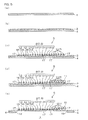
- FIG. 5 is a production process view of a producing method of the COF board shown in FIG. 1 , which is a cross-sectional view along the line A-A of FIG. 2 .
- an IC chip not shown is mounted on the COF board 1.
- the COF board 1 is mounted on various electronic equipment such as a liquid crystal display (a liquid crystal television and the like), and includes an insulating base layer 2 as a belt-like insulating layer continuously extending in a longitudinal direction, a plurality of wiring portions 3 formed on the insulating base layer 2 and provided with conductive patterns 6, and a reinforcing layer 4 (see FIG. 4 ) formed under the insulating baser layer 2.
- the plurality of wiring portions 3 are provided in succession on the surface of the insulating base layer 2 to be spaced apart from each other in a longitudinal direction (which is the same as the longitudinal direction of the COF board 1, and may be hereinafter merely referred to as the "longitudinal direction") of the insulating base layer 2.
- a mounting portion 5 for mounting (placing) an electronic component such as an IC chip not shown is provided at the center portion thereof.
- the mounting portion 5 has a generally rectangular shape when viewed in plan view. On both longitudinal sides of the mounting portion 5, the respective conductive patterns 6 are formed.
- the conductive patterns 6 are made of a plurality of wires 7 arranged in mutually spaced-apart relation on the surface of the insulating base layer 2.
- Each of the wires 7 integrally includes an inner lead 8 and an outer lead 9, each as a terminal portion to be electrically connected to the electronic component, and a middle lead 10.
- the inner leads 8 face the interior of the mounting portion 5, and are arranged in parallel in a widthwise direction (which is perpendicular to the longitudinal direction, and may be hereinafter merely referred to as the "widthwise direction") of the COF board 1.
- the inner lead 8 includes a first inner lead 12 as a first lead, and a second inner lead 13 as a second lead.
- a plurality of the first inner leads 12 are each formed in a generally rectangular shape extending in the longitudinal direction when viewed in plan view, and arranged in a spaced-apart relation in the widthwise direction.
- a plurality of the second inner leads 13 are each formed in a generally rectangular shape extending in the longitudinal direction when viewed in plan view, and arranged in the widthwise direction to be interposed between the mutually adjacent first inner leads 12.
- the plurality of second inner leads 13 are arranged to form, when the first inner leads 12 are projected in the widthwise direction (in the adjacent direction of the mutually adjacent first inner leads 12), overlap portions 14 where the second inner leads 13 overlap with the first leads, and non-overlap portions 15 where the second inner leads 13 do not overlap with the first leads are formed.
- the first inner leads 12 and the second inner leads 13 are arranged such that the base end portions (left end portions in FIG.
- the second inner lead 13 is formed such that the length L4 thereof in the longitudinal direction is smaller than the length L3 of the first inner leads 12 in the longitudinal direction.
- the portions projected from the base end portions of the second inner leads 13 to the free end portions of the second inner leads 13 in the widthwise direction serve as the overlap portions 14, and the portions projected from the free end portions of the second inner leads 13 to the free end portions serve as the non-overlap portions 15.
- the free end portions of the first inner leads 12 and the free end portions of the second inner leads 13 are formed in an alternating and staggered arrangement along the widthwise direction.
- Dummy leads 16 are provided at the non-overlap portions 16.
- the dummy leads 16 are each formed in a generally rectangular shape extending in the longitudinal direction when viewed in plan view. At the non-overlap portions 15, the dummy leads 16 are arranged between the mutually adjacent first inner leads 12, and formed to correspond to the respective second inner leads 13. Each of the dummy leads 16 is disposed at a distance SD away from the individual second inner lead 13 in the longitudinal direction to face the interior of the mounting portion 5. The dummy leads 16 are disposed such that the free end surfaces (right end surfaces in FIG. 3 ) thereof are flush with the free end surfaces (right end surfaces in FIG. 3 ) of the first inner leads 12 in the widthwise direction.
- a width (length in the widthwise direction) W1 of each of the first inner leads 12 and a width (length in the widthwise direction) W2 of each of the second inner leads 13 may be the same or different, and are in a range of, e.g., 5 to 25 ⁇ m, or preferably 10 to 20 ⁇ m.
- a distance (spacing in the widthwise direction) S1 between the first inner lead 12 and the second inner lead 13 adjacent to each other is in a range of, e.g., 5 to 35 ⁇ m, or preferably 10 to 20 ⁇ m.
- a pitch i.e., the total length of the width W1 of one of the first inner leads 12 or the width W2 of one of the second inner leads 13 and the distance (spacing in the widthwise direction) S1 between the first inner lead 12 and the second inner lead 13 adjacent to each other
- IP of each of the inner leads 8 is in a range of, e.g., not more than 50 ⁇ m, or preferably not more than 35 ⁇ m, and normally not less than 15 ⁇ m.
- a length (length in the longitudinal direction from the base end portion to the free end portion) L3 of the first inner lead 12 is in a range of, e.g., 150 ⁇ m to 300 ⁇ m, or preferably 200 to 250 ⁇ m.
- a length (spacing in the longitudinal direction from the proximal end portion to the free end portion) L4 of the second inner lead 13 is in a range of, e.g., 100 ⁇ m to 250 ⁇ m, or preferably 150 to 200 ⁇ m.
- a width WD of the dummy lead 16 is set to be smaller than a width W4 of the bump 18 on the connection terminal of the IC chip described later. That is, the width WD of the dummy lead 16 is set to satisfy the relation given by the following formula (1): WD ⁇ W ⁇ 4
- the width WD of the dummy lead 16 is in the range shown above, it is possible to provide a sufficient spacing (space) between the dummy lead 16 and the second inner lead 13 adjacent thereto, and increase the density of the inner leads 8.
- the width WD of the dummy lead 16 is set to be smaller than or the same as, e.g., the width W2 of the second inner lead 13, i.e., to satisfy the relation given by the following formula (2). WD ⁇ W ⁇ 2
- the width WD of the dummy lead 16 is within the range shown above, it is possible to provide a sufficient spacing (space) between the dummy lead 16 and the second inner lead 13 adjacent thereto, and increase the density of the inner leads 8.
- the width WD of each of the dummy leads 16 is in a range of, e. g. , not less than 8 ⁇ m, or preferably not less than 10 ⁇ m, and normally not more than 15 ⁇ m.
- the distance (spacing in the longitudinal direction) SD between the dummy lead 16 and the second inner lead 13 is set to satisfy the relation given by, e.g., the following formula (3), or more preferably the relation given by the following formula (4).
- a length (length in the longitudinal direction) LD of the dummy lead 16 is preferably set to be larger than the distance SD between the dummy lead 16 and the second inner lead 13.
- non-overlap portions V1 corresponds to the area of the extended portion of the second inner lead 13 obtained by virtually extending the second inner lead 13 toward the interior (right side in FIG. 3 ) of the mounting portion 5.
- the length LD of the dummy lead 16 is in a range of, e.g., 50 to 200 ⁇ m, or preferably 50 to 150 ⁇ m.
- the outer leads 9 each face the both longitudinal end portions of the wiring portions 3, extend along the longitudinal direction, and are arranged in parallel to be spaced apart from each other in the widthwise direction.
- a pitch i.e., the total length of the width (length in the widthwise direction) of the outer lead 9 and the distance (spacing in the widthwise direction) between the two outer leads 9)
- OP of each of the outer leads 9 is set to, e.g., about 100 to 1000% of the pitch IP of each of the inner leads 8.
- the pitch OP of each of the outer leads 9 may be set wider than the pitch IP of each of the inner leads 8, or can also be set as wide as the pitch IP of each of the inner leads 8.
- Each of the middle leads 10 is interposed between each inner lead 8 and each outer lead 9 to provide relay therebetween such that the inner lead 8 is continued to the outer lead 9.
- the pitch OP of each of the outer leads 9 is set wider than the pitch IP of each of the inner leads 8
- the middle leads 10 are arranged in a radial configuration gradually expanding from the inner leads 8 with the narrower pitch toward the outer leads 9 with the wider pitch.
- an insulating cover layer 11 such as a solder resist is provided. That is, the insulating cover layer 11 is formed in a generally rectangular shape when viewed in plan view so as to surround the mounting portion 5, and provided so as to cover all the middle leads 10.
- metal thin films 17 are interposed between the insulating base layer 2, and the conductive patterns 6 and the dummy leads 16, as shown in FIG. 5(e) .
- the inner leads 8 and the outer leads 9 each exposed from the insulating cover layer 11 are each formed with a metal plating layer not shown.
- the reinforcing layer 4 is laminated on the back surface of the insulating baser layer 2.
- openings 19 are formed at positions opposing the respective wiring portions 3, as shown in FIGS. 1 and 4 .
- Each of the openings 19 is formed by opening the reinforcing layer 4 in a generally rectangular shape when viewed from the bottom side in correspondence to each of the wiring portions 3.
- the reinforcing layer 4 reinforces the insulating base layer 2 from thereunder.
- the reinforcing layer 4 is prepared in the method.
- a reinforcing material used to form the reinforcing layer 4 include metal materials such as copper and stainless steel.
- metal materials such as copper and stainless steel.
- stainless steel is used.
- the thickness of the reinforcing layer 4 is in a range of, e.g., 3 to 100 ⁇ m, or preferably 5 to 30 ⁇ m.
- the insulating base layer 2 is formed on the reinforcing layer 4.
- Examples of an insulating material used to form the insulating base layer 2 include synthetic resins such as a polyimide resin, a polyether nitrile resin, a polyether sulfone resin, a polyethylene terephthalate resin, a polyethylene naphthalate resin, and a polyvinyl chloride resin.
- synthetic resins such as a polyimide resin, a polyether nitrile resin, a polyether sulfone resin, a polyethylene terephthalate resin, a polyethylene naphthalate resin, and a polyvinyl chloride resin.
- a photosensitive synthetic resin is preferably used, or more preferably a photosensitive polyimide resin is used.
- a photosensitive synthetic resin is coated on the entire surface of the reinforcing layer 4, dried, exposed to light in the foregoing pattern, developed, and then cured as necessary.
- the insulating base layer 2 can also be formed in the foregoing pattern by a method in which a solution of the synthetic resin mentioned above is uniformly coated on the entire surface of the reinforcing layer 4, dried, cured by heating as necessary, and then etched, or the like. Otherwise, the insulating base layer 2 can be formed by, e.g., preliminarily forming a synthetic resin into a film in the foregoing pattern, and then sticking the film to the surface of the reinforcing layer 4 via a known adhesive layer.
- the thickness of the insulating baser layer 2 thus formed is in a range of, e.g., not more than 50 ⁇ m, or preferably not more than 30 ⁇ m, and normally not less than 3 ⁇ m.
- Examples of a material used to form the conductive patterns 6 and the dummy leads 16 include metal materials (conductive materials) such as copper, nickel, gold, a solder, and an alloy thereof. Preferably, copper is used.
- a known patterning method such as, e.g., an additive method or a subtractive method is used.
- an additive method using electrolytic plating is used.
- the metal thin film 17 is formed first on the entire surface of the insulating base layer 2 by a sputtering method or the like. Then, on the metal thin film 17, a plating resist is formed in a pattern reverse to the conductive patterns 6, and to a pattern of the dummy leads 16. Thereafter, the COF board 1 in the process of the production thereof is dipped in a plating solution of the metal material mentioned above, and electrolytic plating is performed by energizing the dipped COF board 1 to simultaneously form the conductive patterns 6 and the dummy leads 16 on the metal thin film 17 exposed from the plating resist. Thereafter, the plating resist and the portion of the metal thin film 17 where the plating resist is formed are removed.
- the dummy leads 16 are formed between the adjacent first inner leads 12. Therefore, it is possible to substantially equalize the concentration of metal ions in the plating solution in the vicinity of the first inner lead 12, and the concentration of metal ions in the plating solution in the vicinity of the dummy leads 16 and non-overlap portion 14 of the second inner leads 13. Accordingly, the difference between the thickness of the first inner lead 12 and that of the second inner lead 13, which is described later, can be set to not more than 2.0 ⁇ m.
- the conductive patterns 6 are formed as a pattern of the wires 7 integrally formed with the inner leads 8, the outer leads 9, and the middle leads 10, while the dummy leads 16 are formed at the non-overlap portions 15.
- the respective thicknesses of the conductive patterns 6 and the dummy leads 16 thus formed are in a range of, e.g., not less than 5 ⁇ m, or preferably 8 to 15 ⁇ m.
- the thickness of the first inner lead 12 and that of the second inner lead 13 are normally the same, or slightly different. When the thickness of the first inner lead 12 and that of the second inner lead 13 are slightly different, the difference therebetween is in a range of, e.g., not more than 2.0 ⁇ m, or preferably not more than 1. 0 ⁇ m. When the thickness difference between the first inner lead 12 and the second inner lead 13 is over 2.0 ⁇ m, defective connection may be caused in the connection with the connection terminal of the IC chip.
- the insulating cover layer 11 is formed on the insulating base layer 2 so as to cover the middle leads 10.
- an insulating material used to form the insulating cover layer 11 include a synthetic resin such as a solder resist.
- a photosensitive solder resist is formed by a known method which involves exposure to light and development.
- the thickness of the insulating cover layer 11 thus formed is in a range of, e.g., 5 to 30 ⁇ m, or preferably 5 to 20 ⁇ m.
- a metal plating layer not shown is formed on the surfaces of the inner leads 8 and the outer leads 9 of the respective wires 7.
- a metal material used to form the metal plating layer include nickel and gold.
- the metal plating layer is formed by, e.g., electroless metal plating.
- the openings 19 are formed in the reinforcing layer 4.
- the portions of the reinforcing layer 4 opposing the wiring portions 3 are opened by a known method such as, e. g. , chemical etching (wet etching).
- connection terminals for electrically connecting to the inner leads 8 and the outer leads 9, and the bumps 18 (indicated by the imaginary lines in FIG. 3 ) formed on the surfaces of the connection terminals are provided, though not shown.
- the connection terminals for connecting to the inner leads 8 are formed in a pattern (arrangement) corresponding to the alternating and staggered arrangement of the free end portions (indicated by the imaginary lines) of the first inner leads 12 and the free end portions (indicated by the imaginary lines) of the second inner leads 13, as shown in FIG. 3 .
- the width W4 of the bump 18 on the connection terminal corresponding to the inner lead 8 is in a range of, e.g., 10 to 25 ⁇ m, or preferably 15 to 20 ⁇ m.
- the IC chips are placed on the mounting portions 5 of the COF board 1, and the connection terminals of the IC chips are electrically connected to the inner leads 8 and the outer leads 9 via the bumps 18.
- the IC chips can be mounted on the COF board 1.
- the first inner leads 12 and the second inner leads 13 are formed in the alternating and staggered arrangement along the widthwise direction. This allows an increase in the density of the inner leads 8.
- the dummy leads 16 are provided at the non-overlap portions 15 of the COF board 1. Therefore, in the formation of the inner leads 8 by plating in an additive method or the like, it is possible to prevent density unevenness of the inner leads 8 with respect to a plating solution, and equalize the concentration of metal ions in the plating solution in the vicinity of the first inner lead 12, and the concentration of metal ions in the plating solution in the vicinity of the dummy leads 16 and the overlap portions of the second inner leads 13. This allows the first inner lead 12 and the second inner lead 13 to have equal thicknesses. As a result, it is possible to unify the thickness of the inner lead 8, and obtain excellent connection reliability in the COF board 1.
- the mounting portion 5 can be reinforced when the IC chip is mounted.
- first inner leads 12 and the second inner leads 13 are formed in the inner leads 8, and the dummy leads 16 are provided at the non-overlap portions 15 formed with the second inner leads 13.
- first outer leads and second outer leads may be found in the outer leads 9 to provide dummy leads at non-overlap portions formed with the second outer leads, though not shown.
- the plurality of dummy leads 16 are formed in correspondence to the plurality of second inner leads 13.
- portions where the dummy leads 16 are disposed between the adjacent first inner leads 12, and portions where the dummy leads 16 are not disposed between the adjacent first inner leads 12 are regularly or irregularly arranged along the widthwise direction.
- the reinforcing layer 4 is formed in the COF board 1.
- the COF board 1 is formed by laminating the insulating base layer 3, the conductive patterns 6, and the insulating cover layer 11 on a known release sheet, and then removing the release sheet.
- a reinforcing layer made of a stainless steel foil having a thickness of 20 ⁇ m was prepared (see FIG. 5(a) ). Then, a solution of a polyamic acid resin was coated on the entire surface of the reinforcing layer, dried, exposed to light, developed, and then cured by heating to form an insulating base layer made of a polyimide resin and having a thickness of 25 ⁇ m (see FIG. 5(b) ).
- a chromium thin film having a thickness of 30 nm and a copper thin film having a thickness of 200 nm were formed in this order by a sputtering method to form a metal thin film.
- a plating resist made of a dry film resist was formed in a pattern reverse to the conductive patterns, and to a pattern of the dummy leads.
- the conductive patterns and the dummy leads were formed on the metal thin film exposed from the plating resist by electrolytic copper plating.
- the plating resist and the portion of the metal thin film where the plating resist was laminated were removed so that the conductive patterns were formed as a pattern of wires integrally formed with inner leads, outer leads, and middle leads, and dummy leads (each having a thickness of 10 ⁇ m) were formed at non-overlap portions (see FIG. 5(c) ).
- the pitch of the inner lead was 30 ⁇ m, and the pitch of the outer lead was 100 ⁇ m.
- the length of the first inner lead was 300 ⁇ m, and the length of the second inner lead was 150 ⁇ m.
- the other dimensions of the inner leads and the dummy lead were as shown below in Table 1.
- a photosensitive solder resist was formed in a predetermined pattern, exposed to light, and developed to form an insulating cover layer in a pattern covering the middle leads.
- COF boards of EXAMPLES 2 to 5 were obtained in the same manner as in EXAMPLE 1 except that the dimensions of the inner leads and the dummy lead were changed as shown below in Table 1 in the formation of the conductive patterns.
- a COF board was obtained in the same manner as in EXAMPLE 1 except that the dummy leads were not formed in the formation of the conductive patterns.
- Table 1 Examples/ Comparative Examples Dimensions of Terminal Portion ( ⁇ m) Width WD of Dummy Lead Length LD of Dummy Lead Width W2 of Second Lead Width W1 of First Lead Length L1 of Non-Overlap Portion Spacing SD between Dummy Lead and Second Lead Area VD of Dummy Lead Area V1 of Extended Portion Width W4 of Bump Thickness T1 of First Lead Thickness T2 of Second Lead T1- T2
- Example 1 10 50 10 10 150 50 500 1500 20 10.5 8.5 1.4
- Example 2 10 100 10 10 150 20 1000 1500 20 9.3 8.6 0.7
- Example 3 10 160 10 10 180 20 1600 1800 20 8.7 8.9 - 0.2
- Example 4 20 80 10 10 150 30 1600 1500 20 7.9 8.4 - 0.5
- Example 5 20 100 10 10 150 50 2000 1500 20 7.2 8.4 -
- the width (W4) of the bump on the connection terminal corresponding to the inner lead was 20 ⁇ m.
- the IC chips were placed on the respective mounting portions of the COF boards obtained in the examples and the comparative example, and the connection terminals of the IC chip were electrically connected to the inner leads and the outer leads via the bumps.
Landscapes
- Engineering & Computer Science (AREA)
- Microelectronics & Electronic Packaging (AREA)
- Wire Bonding (AREA)
- Structure Of Printed Boards (AREA)
- Coils Or Transformers For Communication (AREA)
Applications Claiming Priority (1)
| Application Number | Priority Date | Filing Date | Title |
|---|---|---|---|
| JP2007264797A JP2009094361A (ja) | 2007-10-10 | 2007-10-10 | Cof基板 |
Publications (2)
| Publication Number | Publication Date |
|---|---|
| EP2048922A2 true EP2048922A2 (de) | 2009-04-15 |
| EP2048922A3 EP2048922A3 (de) | 2010-04-21 |
Family
ID=40291264
Family Applications (1)
| Application Number | Title | Priority Date | Filing Date |
|---|---|---|---|
| EP08162744A Withdrawn EP2048922A3 (de) | 2007-10-10 | 2008-08-21 | COF-Platte |
Country Status (6)
| Country | Link |
|---|---|
| US (1) | US7659605B2 (de) |
| EP (1) | EP2048922A3 (de) |
| JP (1) | JP2009094361A (de) |
| KR (1) | KR20090037333A (de) |
| CN (1) | CN101409274A (de) |
| TW (1) | TW200917427A (de) |
Families Citing this family (15)
| Publication number | Priority date | Publication date | Assignee | Title |
|---|---|---|---|---|
| EP1987533A1 (de) * | 2006-02-15 | 2008-11-05 | Nxp B.V. | Nicht leitende planarisierung einer substratoberfläche für eine formkappe |
| JP5184115B2 (ja) * | 2008-01-31 | 2013-04-17 | 日東電工株式会社 | 配線回路基板およびその製造方法 |
| KR101680115B1 (ko) | 2010-02-26 | 2016-11-29 | 삼성전자 주식회사 | 반도체칩, 필름 및 그를 포함하는 탭 패키지 |
| KR101146987B1 (ko) | 2010-05-03 | 2012-05-23 | 삼성모바일디스플레이주식회사 | 표시장치 및 표시장치에 구비된 구동칩실장용필름소자 |
| US20120007235A1 (en) * | 2010-07-08 | 2012-01-12 | Chao-Chih Hsiao | Chip Fanning Out Method and Chip-on-Film Device |
| JP2012156309A (ja) * | 2011-01-26 | 2012-08-16 | Nitto Denko Corp | 配線回路基板およびその製造方法ならびに燃料電池 |
| CN102510675A (zh) * | 2011-10-25 | 2012-06-20 | 深南电路有限公司 | 载板表面电镀的方法 |
| KR101983374B1 (ko) * | 2012-11-06 | 2019-08-29 | 삼성디스플레이 주식회사 | 표시 패널, 칩 온 필름, 및 이들을 포함하는 표시 장치 |
| KR102059942B1 (ko) | 2013-07-24 | 2019-12-30 | 삼성디스플레이 주식회사 | 유기 발광 표시 장치 |
| US11259406B2 (en) * | 2018-11-21 | 2022-02-22 | Synaptics Incorporated | Flexible connector for a display device |
| US11698695B2 (en) * | 2019-06-27 | 2023-07-11 | Chengdu Boe Optoelectronics Technology Co., Ltd. | Chip on flex, touch assembly, and display device |
| JP2021097233A (ja) * | 2019-12-18 | 2021-06-24 | 日東電工株式会社 | 配線回路基板 |
| JP6970230B2 (ja) * | 2020-03-24 | 2021-11-24 | 日東電工株式会社 | 配線回路基板集合体シート |
| JP2024072219A (ja) * | 2022-11-15 | 2024-05-27 | 日東電工株式会社 | 配線回路基板の製造方法、ダミーパターン付き配線回路基板、および、集合体シート |
| TW202505951A (zh) * | 2023-07-25 | 2025-02-01 | 頎邦科技股份有限公司 | 軟性電路板之內引線結構 |
Citations (1)
| Publication number | Priority date | Publication date | Assignee | Title |
|---|---|---|---|---|
| JP2005183465A (ja) | 2003-12-16 | 2005-07-07 | Nitto Denko Corp | 配線回路基板 |
Family Cites Families (8)
| Publication number | Priority date | Publication date | Assignee | Title |
|---|---|---|---|---|
| JP4197070B2 (ja) * | 1999-04-01 | 2008-12-17 | イビデン株式会社 | 多層ビルドアップ配線板 |
| JP3536023B2 (ja) * | 2000-10-13 | 2004-06-07 | シャープ株式会社 | Cof用テープキャリアおよびこれを用いて製造されるcof構造の半導体装置 |
| JP2002204055A (ja) * | 2000-12-28 | 2002-07-19 | Airex Inc | プリント基板製造方法 |
| TWI233714B (en) * | 2003-12-23 | 2005-06-01 | Himax Tech Inc | Electrical connection structure |
| JP4651367B2 (ja) * | 2004-05-27 | 2011-03-16 | ルネサスエレクトロニクス株式会社 | 半導体装置および半導体装置の製造方法 |
| JP4485460B2 (ja) * | 2004-12-16 | 2010-06-23 | 三井金属鉱業株式会社 | フレキシブルプリント配線板 |
| KR100652519B1 (ko) * | 2005-07-18 | 2006-12-01 | 삼성전자주식회사 | 듀얼 금속층을 갖는 테이프 배선기판 및 그를 이용한 칩 온필름 패키지 |
| JP2007035869A (ja) * | 2005-07-26 | 2007-02-08 | Nitto Denko Corp | Tab用テープキャリア |
-
2007
- 2007-10-10 JP JP2007264797A patent/JP2009094361A/ja active Pending
-
2008
- 2008-08-21 EP EP08162744A patent/EP2048922A3/de not_active Withdrawn
- 2008-09-25 US US12/232,883 patent/US7659605B2/en not_active Expired - Fee Related
- 2008-10-07 TW TW097138511A patent/TW200917427A/zh unknown
- 2008-10-09 KR KR1020080099146A patent/KR20090037333A/ko not_active Withdrawn
- 2008-10-09 CN CNA200810166512XA patent/CN101409274A/zh active Pending
Patent Citations (1)
| Publication number | Priority date | Publication date | Assignee | Title |
|---|---|---|---|---|
| JP2005183465A (ja) | 2003-12-16 | 2005-07-07 | Nitto Denko Corp | 配線回路基板 |
Also Published As
| Publication number | Publication date |
|---|---|
| TW200917427A (en) | 2009-04-16 |
| JP2009094361A (ja) | 2009-04-30 |
| US20090096069A1 (en) | 2009-04-16 |
| CN101409274A (zh) | 2009-04-15 |
| US7659605B2 (en) | 2010-02-09 |
| EP2048922A3 (de) | 2010-04-21 |
| KR20090037333A (ko) | 2009-04-15 |
Similar Documents
| Publication | Publication Date | Title |
|---|---|---|
| EP2048922A2 (de) | COF-Platte | |
| EP1956875A2 (de) | Leiterplatte und Herstellungsverfahren dafür | |
| KR100614864B1 (ko) | 프린트 배선판 및 반도체 장치 | |
| EP2012571A2 (de) | Verbindungsstruktur zwischen einer bestückten Leiterplatte und einem elektronischen Bauteil | |
| KR100578690B1 (ko) | 전자부품 실장용 필름 캐리어 테이프 | |
| US20080087455A1 (en) | Wired circuit board | |
| US10531569B2 (en) | Printed circuit board and method of fabricating the same | |
| US20050244620A1 (en) | Wired circuit board and production method thereof | |
| US20060213684A1 (en) | Flexible printed wiring board, method for fabricating flexible printed wiring board, and semiconductor device | |
| US20040159930A1 (en) | Semiconductor device, method of manufacturing the same, and electronic device using the semiconductor device | |
| EP1819209B1 (de) | Leiterplatte und Verfahren zur Herstellung | |
| US8198017B2 (en) | Producing method of wired circuit board | |
| US7307854B2 (en) | Flexible wired circuit board | |
| US20070023877A1 (en) | Chip on flex tape with dimension retention pattern | |
| KR101477818B1 (ko) | 배선 회로 기판 및 그 제조 방법 | |
| US20070023876A1 (en) | Tab tape carrier | |
| JP2005183464A (ja) | 配線回路基板 | |
| US20060118457A1 (en) | Film carrier tape for mounting electronic component | |
| US20060214282A1 (en) | Flexible printed wiring board, method for fabricating flexible printed wiring board, and semiconductor device | |
| KR100780172B1 (ko) | 탭용 테이프 캐리어 | |
| JP4473847B2 (ja) | フレキシブル配線回路基板およびその製造方法 | |
| KR20220101628A (ko) | 배선 회로 기판 | |
| JP2007103587A (ja) | 配線回路基板およびその製造方法 |
Legal Events
| Date | Code | Title | Description |
|---|---|---|---|
| PUAI | Public reference made under article 153(3) epc to a published international application that has entered the european phase |
Free format text: ORIGINAL CODE: 0009012 |
|
| AK | Designated contracting states |
Kind code of ref document: A2 Designated state(s): AT BE BG CH CY CZ DE DK EE ES FI FR GB GR HR HU IE IS IT LI LT LU LV MC MT NL NO PL PT RO SE SI SK TR |
|
| AX | Request for extension of the european patent |
Extension state: AL BA MK RS |
|
| PUAL | Search report despatched |
Free format text: ORIGINAL CODE: 0009013 |
|
| AK | Designated contracting states |
Kind code of ref document: A3 Designated state(s): AT BE BG CH CY CZ DE DK EE ES FI FR GB GR HR HU IE IS IT LI LT LU LV MC MT NL NO PL PT RO SE SI SK TR |
|
| AX | Request for extension of the european patent |
Extension state: AL BA MK RS |
|
| RIC1 | Information provided on ipc code assigned before grant |
Ipc: H05K 1/18 20060101ALN20100312BHEP Ipc: H05K 1/05 20060101ALN20100312BHEP Ipc: H01L 23/498 20060101ALI20100312BHEP Ipc: H05K 1/11 20060101AFI20090204BHEP |
|
| AKY | No designation fees paid | ||
| STAA | Information on the status of an ep patent application or granted ep patent |
Free format text: STATUS: THE APPLICATION IS DEEMED TO BE WITHDRAWN |
|
| 18D | Application deemed to be withdrawn |
Effective date: 20101022 |
|
| REG | Reference to a national code |
Ref country code: DE Ref legal event code: R108 Effective date: 20110405 Ref country code: DE Ref legal event code: 8566 |